fpga design flow - milwaukee school of engineering · pdf filedesign flow •requirements...
TRANSCRIPT

FPGA Design Flow

2 © tjEE 3921 – Fall 2016
Design Flow
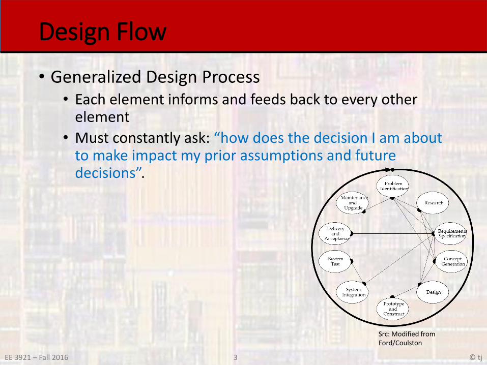
• Generalized Design Process
ProblemIdentification
Research
RequirementsSpecification
ConceptGeneration
Prototypeand
Construct
SystemIntegration
SystemTest
Deliveryand
Acceptance
Maintenanceand
Upgrade
Design
Src: Modified fromFord/Coulston
3 © tjEE 3921 – Fall 2016
Design Flow
• Generalized Design Process• Each element informs and feeds back to every other
element
• Must constantly ask: “how does the decision I am about to make impact my prior assumptions and future decisions”.
Src: Modified fromFord/Coulston

4 © tjEE 3921 – Fall 2016
Design Flow
• Problem Identification
• In most cases you will be given the problem to solve
• It is critical to test this problem identification
• Do you understand the problem
• Is it the fundamental problem or an already half solved problem
• Is it well defined, but not over defined

5 © tjEE 3921 – Fall 2016
Design Flow
• Research
• Understand the underlying principles of the problem
• Review current solutions
• Look for gaps and opportunities to innovate
• Become a subject matter expert

6 © tjEE 3921 – Fall 2016
Design Flow
• Requirements Specification
• Identify what the system must do to solve the problem
• Over specify: • Higher cost• Longer development time
• Under specify• Don’t solve problem• Customer does not accept the solution
• No design solutions should be assumed at this stage
• Maximize the design space

7 © tjEE 3921 – Fall 2016
Design Flow
• Concept Generation
• Multiple design solutions are conceived
• Initially these can be wildly creative
• Each design solution is explored far enough to allow it to be compared to:
• Requirements
• Other possible design solutions
• Typically only one design solution emerges from this phase
8 © tjEE 3921 – Fall 2016
Design Flow
• Design
• Hierarchical system design
• Up/Down sub-system design
• Detailed block, module, circuit, and software design
• Heavy reliance on models and simulation tools
• Tight feedback with prototyping phase
9 © tjEE 3921 – Fall 2016
Design Flow
• Prototyping and Construction
• Used to inform the design process
• Prototype small elements of the design in very tight loops
• Prototype larger elements of the design at critical development points
• For long lead time elements (e.g. Integrated Circuits) it is critical to make the right decisions on prototyping• More design time less time to correct errors found in
prototyping
• Early prototyping more errors higher chance of errors in the fixes

10 © tjEE 3921 – Fall 2016
Design Flow
• System Integration
• Pull everything together
• Happens at multiple levels of the design hierarchy
• Highlights specification errors (between sub-systems)
• Highlights communications errors (between teams)

11 © tjEE 3921 – Fall 2016
Design Flow
• System Test
• Test everything together
• Happens at multiple levels of the design hierarchy
• Validates the system to the original Requirements Specifications
does it solve the original problem

12 © tjEE 3921 – Fall 2016
Design Flow
• Delivery and Acceptance
• In situ testing
• Validate the solution
• Uncover unexpected interdependencies
• Frequently require “tweeks” to the solution or the system
13 © tjEE 3921 – Fall 2016
Design Flow
• Manufacturing
• Determine manufacturability
• Component robustness
• Overall system yield
• Complexity

14 © tjEE 3921 – Fall 2016
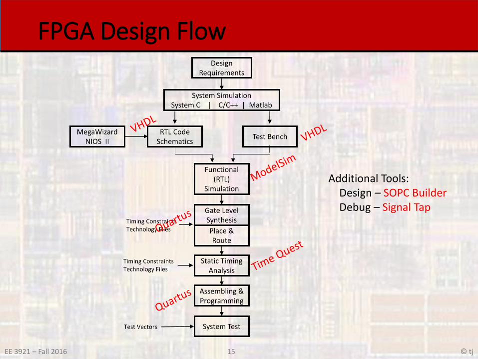
FPGA Design FlowDesign
Requirements
RTL CodeSchematics
Test Bench
Functional(RTL)
Simulation
Gate Level Synthesis
Place & Route
Static Timing Analysis
Assembling & Programming
System Test
Timing ConstraintsTechnology Files
Timing ConstraintsTechnology Files
Test Vectors
System SimulationSystem C | C/C++ | Matlab
MegaWizardNIOS II
15 © tjEE 3921 – Fall 2016
FPGA Design FlowDesign
Requirements
RTL CodeSchematics
Test Bench
Functional(RTL)
Simulation
Gate Level Synthesis
Place & Route
Static Timing Analysis
Assembling & Programming
System Test
Timing ConstraintsTechnology Files
Timing ConstraintsTechnology Files
Test Vectors
System SimulationSystem C | C/C++ | Matlab
Additional Tools:Design – SOPC BuilderDebug – Signal Tap
MegaWizardNIOS II

16 © tjEE 3921 – Fall 2016
Design Flow
• Design Entry• Text entry
• VHDL Files
• Hierarchical instantiation of blocks
• Schematic entry• Quartus Block Editor
• Create bdf schematic files
• Quartus Symbol Editor• Create / modify symbols for the block editor (bsf file)

17 © tjEE 3921 – Fall 2016
Design Flow
• Design Entry• Quartus Block Editor
• File -> New -> Design Files -> Schematic/Block Editor

18 © tjEE 3921 – Fall 2016
Design Flow
• Design Entry• Quartus Block Editor
• Symbol Tool

19 © tjEE 3921 – Fall 2016
Design Flow
• Design Entry• Quartus Block Editor
• Orthogonal Node Tool

20 © tjEE 3921 – Fall 2016
Design Flow
• Design Entry• Quartus Block Editor
• Pin Tool

21 © tjEE 3921 – Fall 2016
Design Flow
• Design Entry• Quartus Block Editor
• File -> Create/Update -> Create Symbol Files for Current File
• Select “all files” then select myFile.bsf

22 © tjEE 3921 – Fall 2016
Design Flow
• Design Entry• Quartus Block Editor
• Buses and wires are connected by name

23 © tjEE 3921 – Fall 2016
Design Flow
• Design Entry• Pin Assignments
• Assignments -> Import Assignments
• Point to the DE1.qsf file
• This has all pins in it
and will generate
warnings later on for
each unused pin
• You can copy and
modify the file to
remove the warnings

24 © tjEE 3921 – Fall 2016
Design Flow
• RTL Synthesis• Analyze VHDL
• Processing -> Analyze Current File
• Finds syntax errors
• Does not check for synthesizability
• Analysis and Elaboration• Processing -> Start -> Start Analysis and Elaboration
• Finds syntax errors
• Check for synthesizability
• Creates RTL• Check for errors – especially unintended latches

25 © tjEE 3921 – Fall 2016
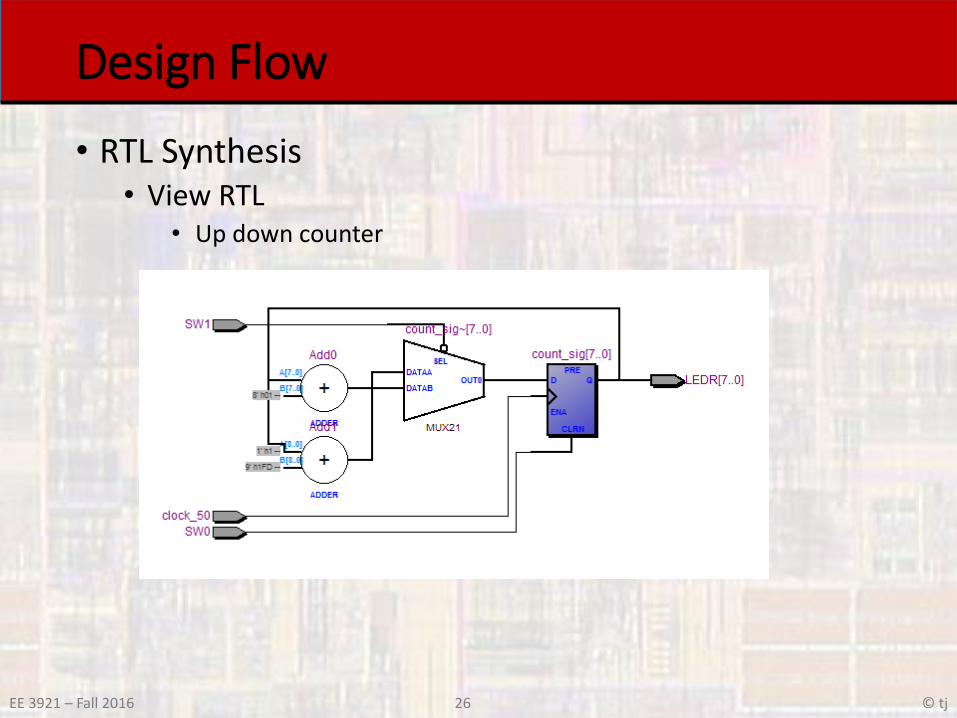
Design Flow
• RTL Synthesis• View RTL
• Tools-> Netlist Viewer -> RTL Viewer
• Does this make sense?
• View State Machines• Tools-> Netlist Viewer -> State Machine Viewer
• Does this make sense?
26 © tjEE 3921 – Fall 2016
Design Flow
• RTL Synthesis• View RTL
• Up down counter

27 © tjEE 3921 – Fall 2016
Design Flow
• RTL Synthesis• View State Machine
• Branch predictor

28 © tjEE 3921 – Fall 2016
Design Flow
• Functional Simulation
• ModelSim via Quartus• Tools -> Run Simulation Tool-> RTL Simulation
• ModelSim stand alone

29 © tjEE 3921 – Fall 2016
Design Flow
• Gate Level Implementation• Analysis and Synthesis
• Processing -> Start -> Analysis and Synthesis
• Maps the RTL to non-specific FPGA blocks
• Partition and Merge• Processing -> Start -> Partition and Merge
• ?????
• Optional Gate Level Simulation• ModelSim via Quartus
• Tools -> Run Simulation Tool-> Gate Level Simulation
• New work directory : gate_work

30 © tjEE 3921 – Fall 2016
Design Flow
• Gate Level Implementation• Technology Map Viewer – Post Mapping
• Up/Down Counter

31 © tjEE 3921 – Fall 2016
Design Flow
• FPGA Implementation • Timing Constraints
• Assignments -> Import Assignments• Point to the Cyclone II.sdc file
• Fitter• Processing -> Start -> Start Fitter• Maps the generalized gate level logic
to specific FPGA blocks• Accounts for loading and timing constraints
• Chip Planner• Tools -> Chip Planner• View the physical implementation• Cross Probe via Locate -> Locate in …

32 © tjEE 3921 – Fall 2016
Design Flow
• FPGA Implementation • Fitter – Resource Usage
33 © tjEE 3921 – Fall 2016
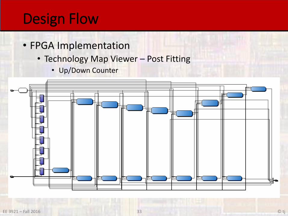
Design Flow
• FPGA Implementation• Technology Map Viewer – Post Fitting
• Up/Down Counter

34 © tjEE 3921 – Fall 2016
Design Flow
• FPGA Implementation • Chip Planner
35 © tjEE 3921 – Fall 2016
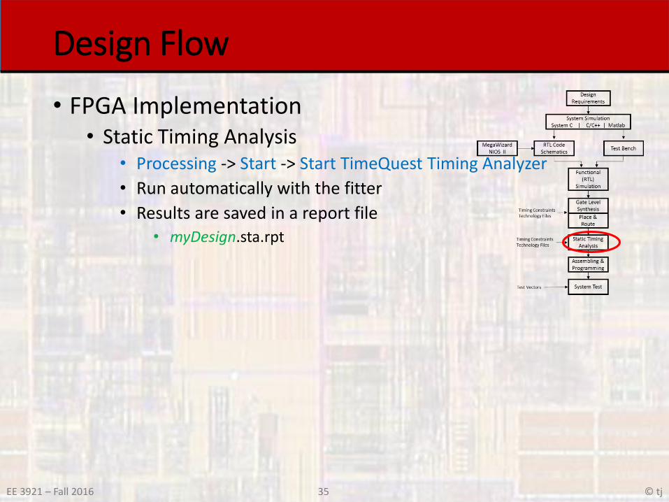
Design Flow
• FPGA Implementation • Static Timing Analysis
• Processing -> Start -> Start TimeQuest Timing Analyzer
• Run automatically with the fitter
• Results are saved in a report file• myDesign.sta.rpt

36 © tjEE 3921 – Fall 2016
Design Flow
• FPGA Implementation • Static Timing Analysis
• Positive Slack - good
• Negative Slack – bad

37 © tjEE 3921 – Fall 2016
Design Flow
• FPGA Implementation • Assembler
• Processing -> Start -> Start Assembler
• Creates the programming file
• Prepares for additional power analysis
• Programming• Tools -> Programmer

38 © tjEE 3921 – Fall 2016
Design Flow
• FPGA Implementation • Assembler
• Processing -> PowerPlay Power Analyzer Tool

39 © tjEE 3921 – Fall 2016
Design Flow
• FPGA Implementation • Programmer

40 © tjEE 3921 – Fall 2016
Design Flow
• FPGA Implementation • Programmer Processing -> Start

41 © tjEE 3921 – Fall 2016
Design Flow
• For example, in the qsf file the 18 toggle switches are called SW[17] to SW[0]; since VHDL
• uses parentheses rather than square brackets, these switches are referred to as SW(17) to SW(0). They can also be
• referred to as an array SW(17 downto 0).