fpga basedsystemdesign+ - politecnico di...
TRANSCRIPT

FPGA-‐based System Design
Reconfigurable Hardware
“Reconfigurable computing is intended to fill the gap between hardware and software, achieving potentially much higher
performance than software, while maintaining a higher level of flexibility than hardware”
(K. Compton and S. Hauck, Reconfigurable Computing: a Survey of Systems and Software, 2002)
2
FPGA-‐based System Design
trend toward higher levels of integration
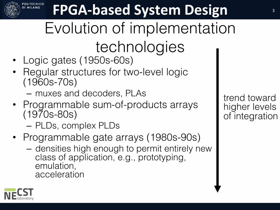
Evolution of implementation technologies
• Logic gates (1950s-60s) • Regular structures for two-level logic
(1960s-70s) – muxes and decoders, PLAs
• Programmable sum-of-products arrays (1970s-80s) – PLDs, complex PLDs
• Programmable gate arrays (1980s-90s) – densities high enough to permit entirely new
class of application, e.g., prototyping, emulation, acceleration
3

FPGA-‐based System Design
Gate Array Technology (IBM - 1970s) • Simple logic gates
– combine transistors to implement combinational and sequential logic
• Interconnect – wires to connect inputs and
outputs to logic blocks • I/O blocks
– special blocks at periphery for external connections
• Add wires to make connections – done when chip is fabbed
• “mask-programmable” – construct any circuit
4
FPGA-‐based System Design
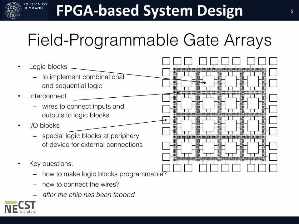
Field-Programmable Gate Arrays • Logic blocks
– to implement combinational and sequential logic
• Interconnect – wires to connect inputs and
outputs to logic blocks • I/O blocks
– special logic blocks at periphery of device for external connections
• Key questions: – how to make logic blocks programmable? – how to connect the wires? – after the chip has been fabbed
5

FPGA-‐based System Design
Commercial FPGA Companies
Lattice official webiste
6

FPGA-‐based System Design
IOB IOB IOB IOB
CLB CLB
CLB CLBIOB
IOB
IOB
IOB
Wiring Channels
Xilinx Programmable Gate Arrays • CLB - Configurable Logic
Block • Built-in fast carry logic • Can be used as memory • Three types of routing
– direct – general-purpose – long lines of various lengths
• RAM-programmable – can be reconfigured
7
FPGA-‐based System Design
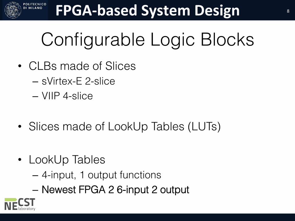
Configurable Logic Blocks • CLBs made of Slices – sVirtex-E 2-slice – VIIP 4-slice
• Slices made of LookUp Tables (LUTs)
• LookUp Tables – 4-input, 1 output functions – Newest FPGA 2 6-input 2 output
8
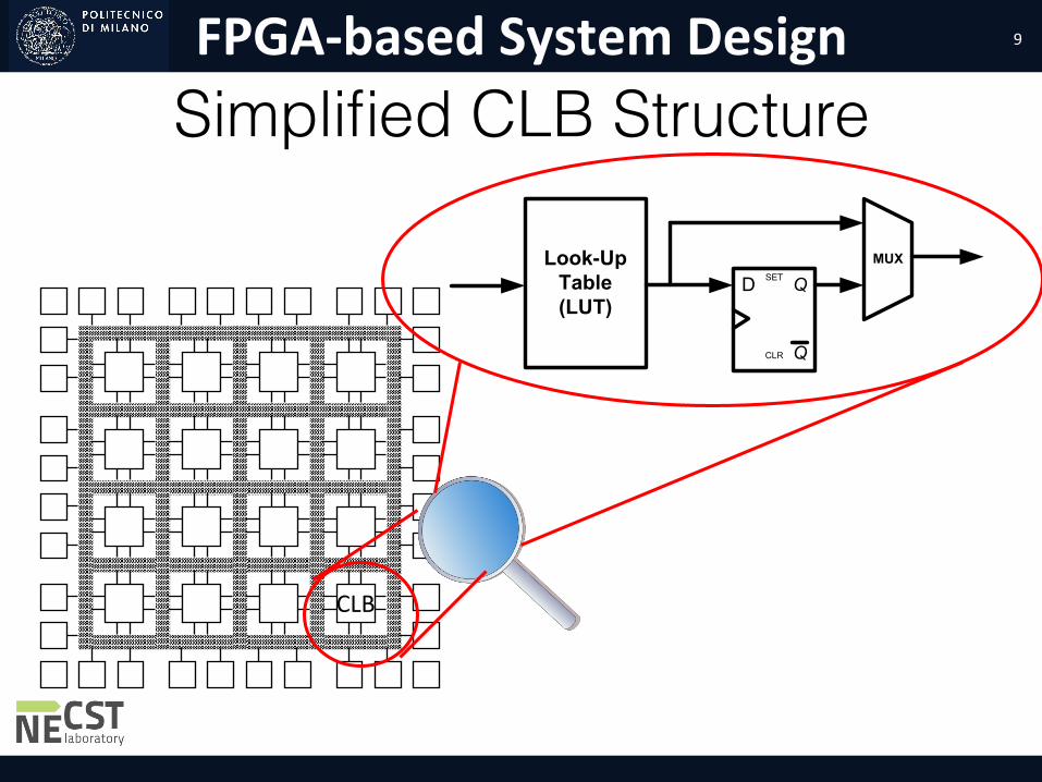
FPGA-‐based System Design Simplified CLB Structure
Look-Up Table (LUT)
Q
QSET
CLR
DMUX
CLB
9
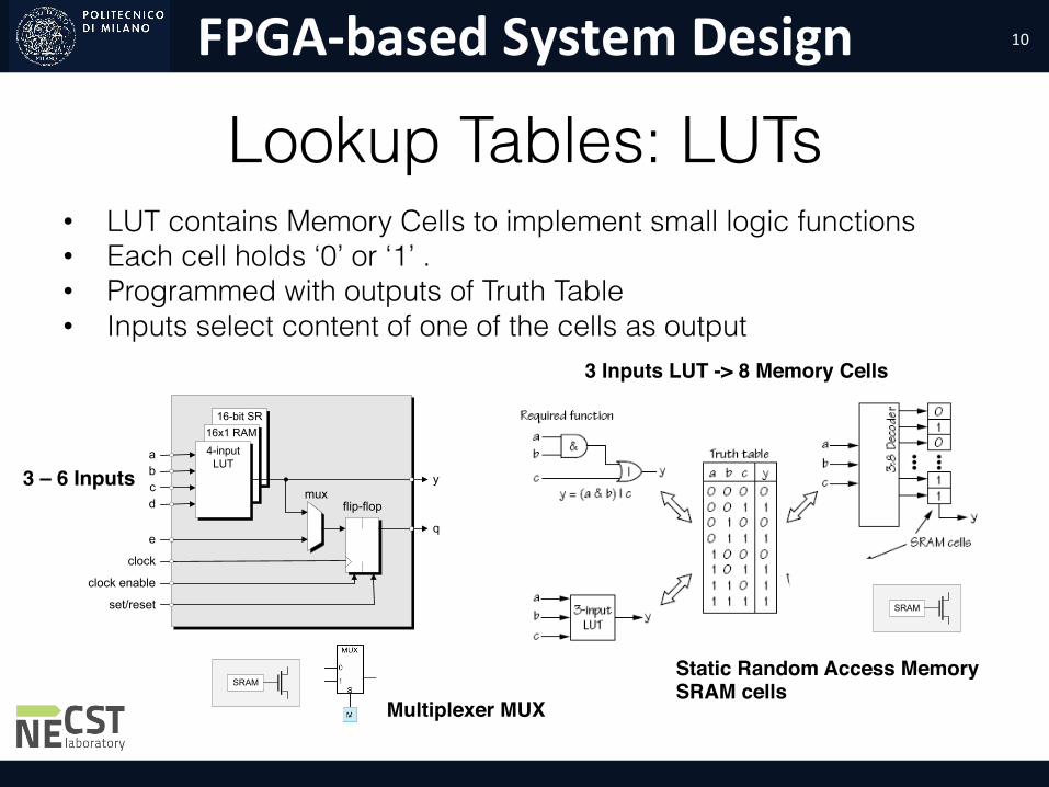
FPGA-‐based System Design
Lookup Tables: LUTs • LUT contains Memory Cells to implement small logic functions • Each cell holds ‘0’ or ‘1’ . • Programmed with outputs of Truth Table • Inputs select content of one of the cells as output
16-bit SR
flip-flop
clock
muxy
qe
abcd
16x1 RAM4-input
LUT
clock enable
set/reset
3 Inputs LUT -> 8 Memory Cells!
SRAM
Static Random Access Memory!SRAM cells!SRAM
3 – 6 Inputs!
Multiplexer MUX!
10
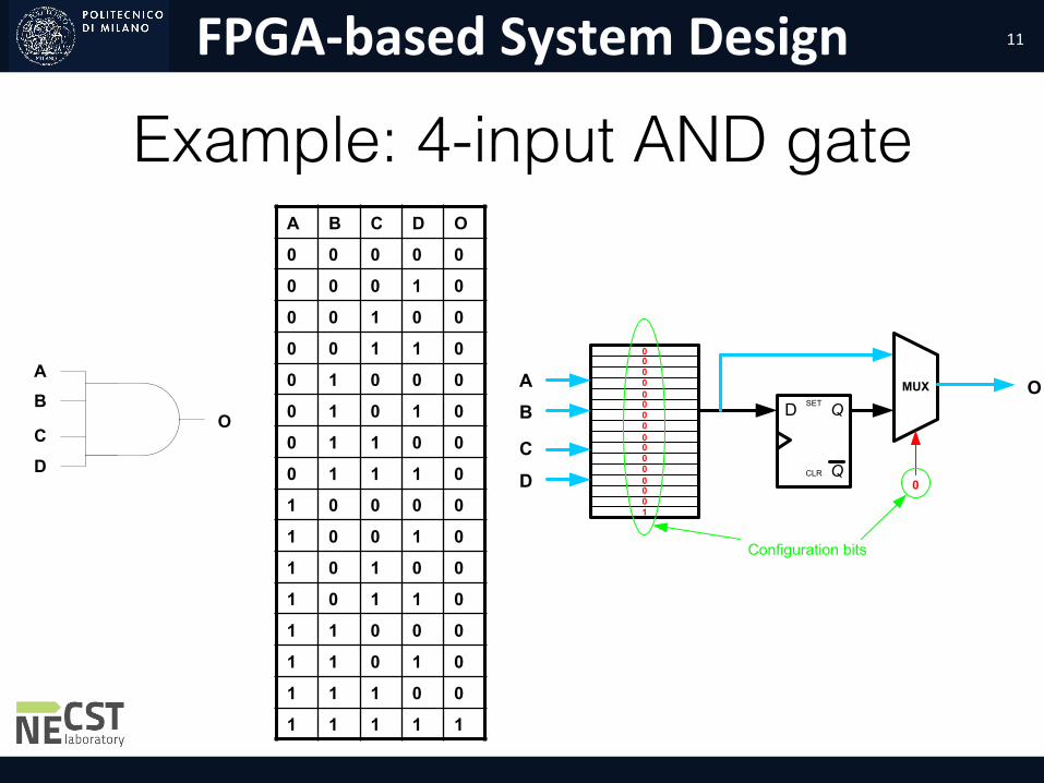
FPGA-‐based System Design
Example: 4-input AND gate
AB
C
D
O
A B C D O
0 0 0 0 0
0 0 0 1 0
0 0 1 0 0
0 0 1 1 0
0 1 0 0 0
0 1 0 1 0
0 1 1 0 0
0 1 1 1 0
1 0 0 0 0
1 0 0 1 0
1 0 1 0 0
1 0 1 1 0
1 1 0 0 0
1 1 0 1 0
1 1 1 0 0
1 1 1 1 1
Q
QSET
CLR
DMUXA
B
C
D
0000000000000001
Configuration bits
O
0
11
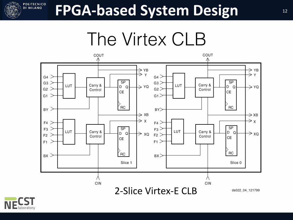
FPGA-‐based System Design
The Virtex CLB
2-‐Slice Virtex-‐E CLB
12

FPGA-‐based System Design
Details of One Virtex Slice
Virtex-‐E Slice

FPGA-‐based System Design
Implements any Two 4-input Functions
4-‐input func>on
3-‐input func>on;
registered
Virtex-‐E Slice
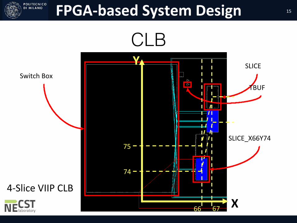
FPGA-‐based System Design
CLB Switch Box
SLICE
TBUF
Y
X 67 66
75
74
SLICE_X66Y74
15
4-‐Slice VIIP CLB
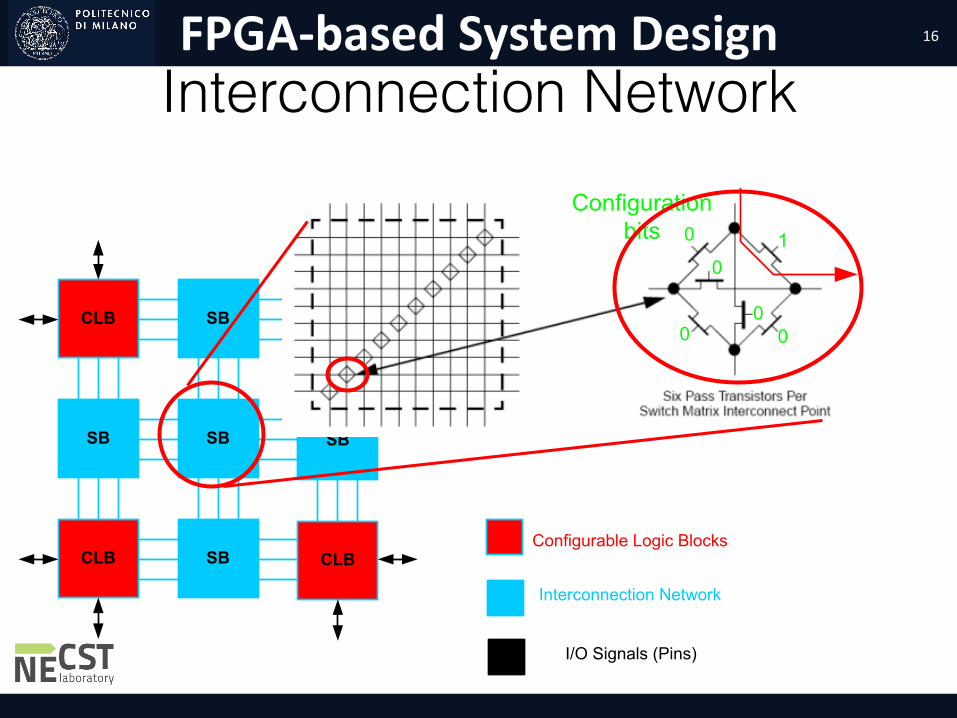
FPGA-‐based System Design Interconnection Network
CLB SB
SB SB
CLB
SB
CLB SB CLBConfigurable Logic Blocks
Interconnection Network
I/O Signals (Pins)
Configuration bits 1
0
0
00
0
16
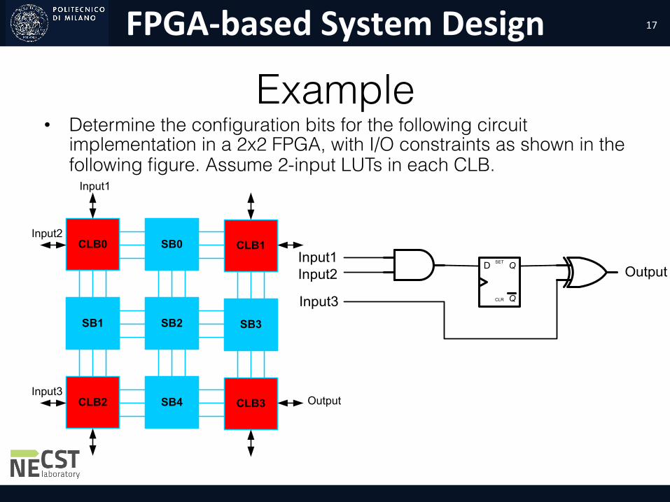
FPGA-‐based System Design
Example
CLB0 SB0
SB1 SB2
CLB1
SB3
CLB2 SB4 CLB3
Input1
Input2
OutputInput3
• Determine the configuration bits for the following circuit implementation in a 2x2 FPGA, with I/O constraints as shown in the following figure. Assume 2-input LUTs in each CLB.
Q
QSET
CLR
DInput1Input2
Input3
Output
17
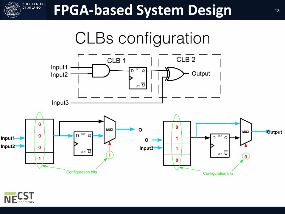
FPGA-‐based System Design
CLBs configuration
Q
QSET
CLR
DInput1Input2
Input3
Output
CLB 1 CLB 2
Q
QSET
CLR
DMUX
Input1Input2
0
0
0
1
Configuration bits
O
1 Q
QSET
CLR
DMUX
OInput3
0
1
1
0
Configuration bits
Output
0
18
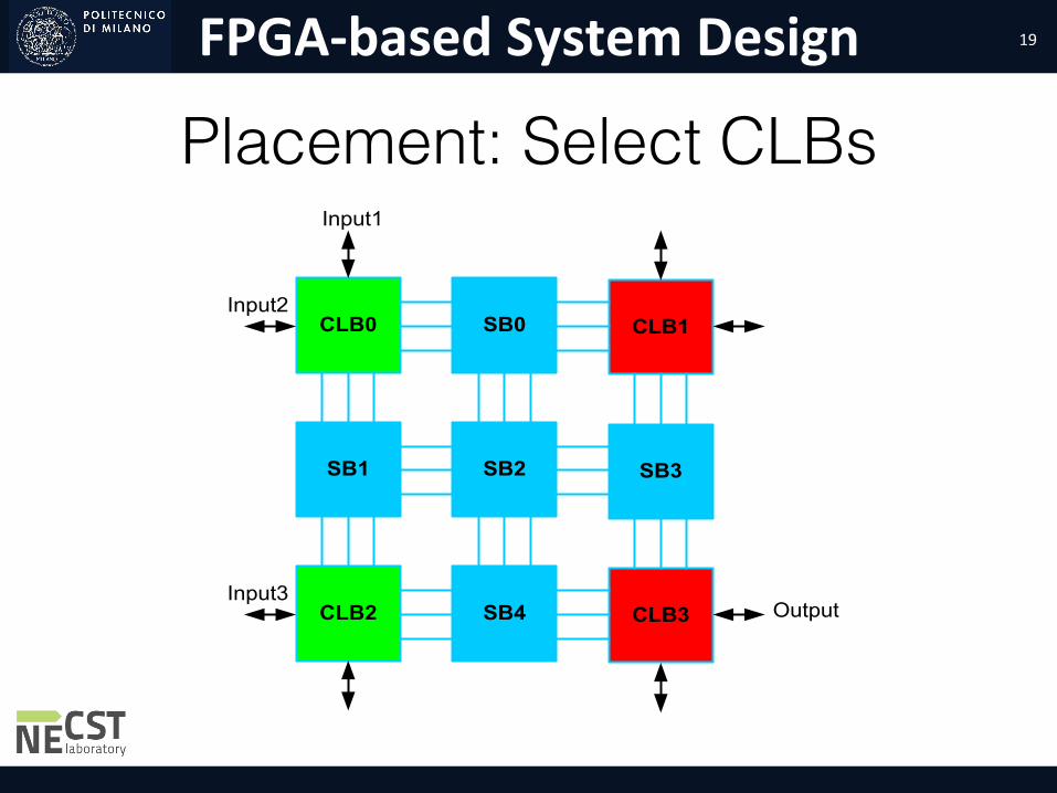
FPGA-‐based System Design
Placement: Select CLBs
CLB0 SB0
SB1 SB2
CLB1
SB3
CLB2 SB4 CLB3
Input1
Input2
OutputInput3
19
FPGA-‐based System Design
Routing: Select path
CLB0 SB0
SB1 SB2
CLB1
SB3
CLB2 SB4 CLB3
Input1
Input2
OutputInput3
Configuration bits
SB1
1
0
0
00
0
Configuration bits
SB4
0
0
0
01
0
20

FPGA-‐based System Design
Configuration Bitstream • The configuration bitstream must include ALL CLBs and
SBs, even unused ones • CLB0: 00011 • CLB1: ????? • CLB2: 01100 • CLB3: XXXXX • SB0: 000000 • SB1: 000010 • SB2: 000000 • SB3: 000000 • SB4: 000001
21

FPGA-‐based System Design
The configuration bitstream
• Occupation must be determined only on the basis of – Number of configuration words – Initial Frame Address Register (FAR) value
22
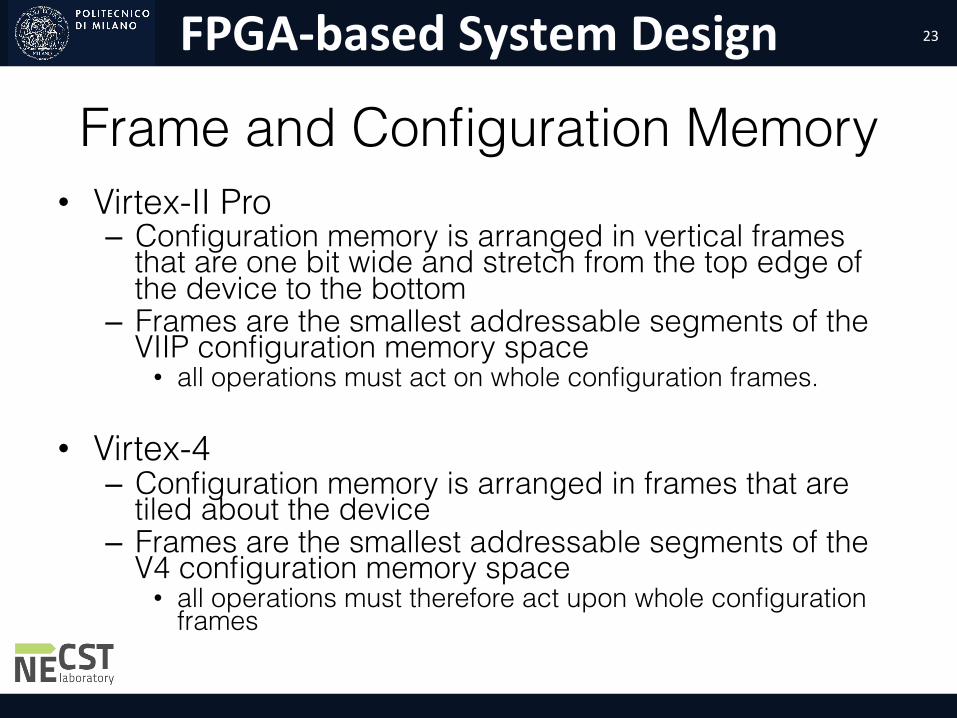
FPGA-‐based System Design
Frame and Configuration Memory • Virtex-II Pro
– Configuration memory is arranged in vertical frames that are one bit wide and stretch from the top edge of the device to the bottom
– Frames are the smallest addressable segments of the VIIP configuration memory space • all operations must act on whole configuration frames.
• Virtex-4 – Configuration memory is arranged in frames that are
tiled about the device – Frames are the smallest addressable segments of the
V4 configuration memory space • all operations must therefore act upon whole configuration
frames
23
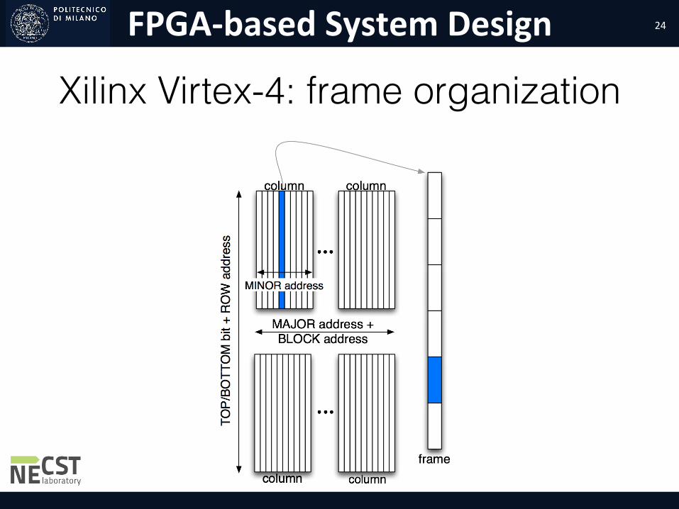
FPGA-‐based System Design
Xilinx Virtex-4: frame organization
24
FPGA-‐based System Design
Some Definitions • Object Code: the executable active physical (either HW or
SW) implementation of a given functionality • Core: a specific representation of a functionality. It is
possible, for example, to have a core described in VHDL, in C or in an intermediate representation (e.g. a DFG)
• IP-Core: a core described using a HD Language combined with its communication infrastructure (i.e. the bus interface)
• Reconfigurable Functional Unit: an IP-Core that can be plugged and/or unplugged at runtime in an already working architecture
• Reconfigurable Region: a portion of the device area used to
implement a reconfigurable core
25
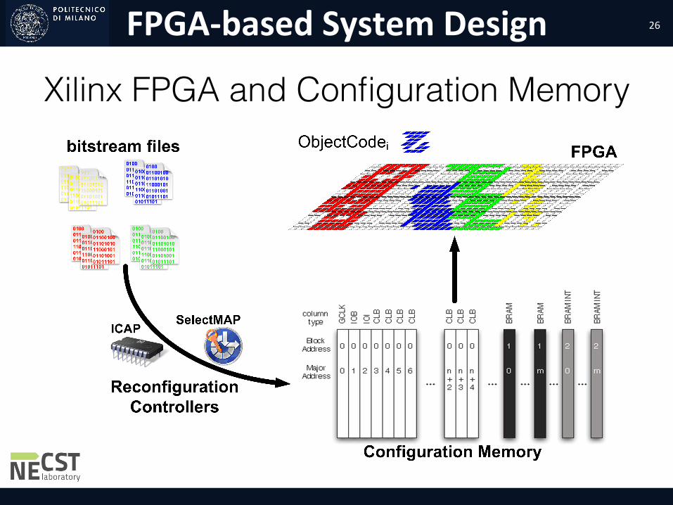
FPGA-‐based System Design
Xilinx FPGA and Configuration Memory
26

FPGA-‐based System Design
FPGA EDA Tools • Must provide a design environment based on
digital design concepts and components (gates, flip-flops, MUXs, etc.)
• Must hide the complexities of placement, routing and bitstream generation from the user. Manual placement, routing and bitstream generation is infeasible for practical FPGA array sizes and circuit complexities.
27

FPGA-‐based System Design
Computer-aided Design • Can't design FPGAs by hand
– way too much logic to manage, hard to make changes
• Hardware description languages – specify functionality of logic at a high level
• Validation - high-level simulation to catch specification errors – verify pin-outs and connections to other system components – low-level to verify mapping and check performance
• Logic synthesis – process of compiling HDL program into logic gates and flip-flops
• Technology mapping – map the logic onto elements available in the implementation
technology (LUTs for Xilinx FPGAs)
28

FPGA-‐based System Design
CAD Tool Path (cont’d) • Placement and routing
– assign logic blocks to functions – make wiring connections
• Timing analysis - verify paths – determine delays as routed – look at critical paths and ways to improve
• Partitioning and constraining – if design does not fit or is unroutable as placed split into multiple chips – if design it too slow prioritize critical paths, fix placement of cells, etc. – few tools to help with these tasks exist today
• Generate programming files - bits to be loaded into chip for configuration
29
FPGA-‐based System Design
QUESTIONS?
30