fpga based digital design using verilog hdl · course title: fpga based digital design using...
TRANSCRIPT

Course Title: FPGA Based Digital Design using Verilog HDL
Course Organized By: Electronics Division, PINSTECH
FPGA Based Digital Design Using Verilog HDL
Course Designed by:
IRFAN FAISAL MIR( Verilog / FPGA Designer )
* Organized by Electronics DivisionPINSTECH, Islamabad
Introductory Class Course Organized By: Electronics Division, PINSTECH, Islamabad
Uses for digital IC technology today:Standard Microprocessors
Used in desktop PC and embedded applications
Memory Chips (RAMs)Application Specific ICs (ASICs)
Custom design to match particular applicationsCan be optimized for low power, low cost, high performance
Integrated Circuits

Course Title: FPGA Based Digital Design using Verilog HDL
Course Organized By: Electronics Division, PINSTECH
Introductory Class Course Organized By: Electronics Division, PINSTECH, Islamabad
Field Programmable Logic Devices (FPGAs, CPLDs)
Customized to parti-cular applicationsReconfigure device Short time to market
Xilinx FPGA
Introductory Class Course Organized By: Electronics Division, PINSTECH, Islamabad
FPGA Basics
FPGA Basics
FPGA stands for “Field Programmable Gate Array”.
SRAM Based FPGAs are most popular due to its reconfigurable feature
FPGA can be categorized as: Anti-fuse based (ex: Actel)SRAM Based (ex: Xilinx, Altera)

Course Title: FPGA Based Digital Design using Verilog HDL
Course Organized By: Electronics Division, PINSTECH
Introductory Class Course Organized By: Electronics Division, PINSTECH, Islamabad
Number of System Gates, Speed Grade, Frequency, No of I/Os and Build in features etc are basic identity of any FPGA
World Popular Xilinx FPGA is typically an SRAM-based device
Introductory Class Course Organized By: Electronics Division, PINSTECH, Islamabad
FPGA is a Programmable Integrated Circuit consisting of:
An internal array ofConfigurable LogicBlocks (CLBs).
Basic FPGA Internal Architecture
Connected together via programmable interconnection.
A ring of programmable input/output blocks.

Course Title: FPGA Based Digital Design using Verilog HDL
Course Organized By: Electronics Division, PINSTECH
Introductory Class Course Organized By: Electronics Division, PINSTECH, Islamabad
Some Popular Xilinx FPGAs:
Spartan II/IIE/III,VirtexTM, Virtex-E and VirtexTM-II devices.Range of Xilinx FPGAs from Few 10K Gates to Multi-Million Gates with Embedded Cores.
Introductory Class Course Organized By: Electronics Division, PINSTECH, Islamabad
Verilog HDL Basics
Verilog HDL BasicsVerilog HDL is a Hardware Description
Language. It describes the hardware.
Open Verilog International (OVI) IEEE 1364
It enables specification of a digital system at a range of levels of abstraction:
Switches, Gates, RTL, and higher
Verilog HDL is a concurrent language
It is not a programming & procedural language.

Course Title: FPGA Based Digital Design using Verilog HDL
Course Organized By: Electronics Division, PINSTECH
Introductory Class Course Organized By: Electronics Division, PINSTECH, Islamabad
Why use an HDL ?Describe complex designs (millions of gates)
Input to synthesis tools (synthesizable subset)
Design exploration with simulation
Why not use a general purpose languageSupport for structure and instantiationSupport for describing bit-level behaviorSupport for timingSupport for concurrency
Introductory Class Course Organized By: Electronics Division, PINSTECH, Islamabad
Verilog vs. VHDLVerilog is relatively simple and close to CVHDL is complex Verilog has 60% of the world digital design market (larger share in US)
Course Title: FPGA Based Digital Design using Verilog HDL
Course Organized By: Electronics Division, PINSTECH
Introductory Class Course Organized By: Electronics Division, PINSTECH, Islamabad
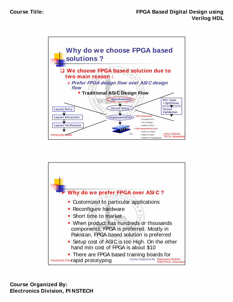
Why do we choose FPGA based solutions ?
We choose FPGA based solution due to two main reason :
Prefer FPGA design flow over ASIC design flow
Traditional ASIC Design Flow
• ASICs Design Cycle
Concept to RTL
RTL to Netlist
Netlist to GDS II
• ASICs Manufacturing Cycle
GDS II to a Mask
Mask to a wafer
Wafer to a Packaged part
RTL Code +Synthesis
Circuit Validation
Layout Entry
Layout Extraction
Layout Verification
Specifications
Circuit Entry
Implementation
Introductory Class Course Organized By: Electronics Division, PINSTECH, Islamabad
Why do we prefer FPGA over ASIC ?
Customized to particular applicationsReconfigure hardwareShort time to marketWhen product has hundreds or thousands
components, FPGA is preferred. Mostly in Pakistan, FPGA based solution is preferredSetup cost of ASIC is too High. On the other
hand min cost of FPGA is about $10There are FPGA based training boards for
rapid prototyping
Course Title: FPGA Based Digital Design using Verilog HDL
Course Organized By: Electronics Division, PINSTECH
Introductory Class Course Organized By: Electronics Division, PINSTECH, Islamabad
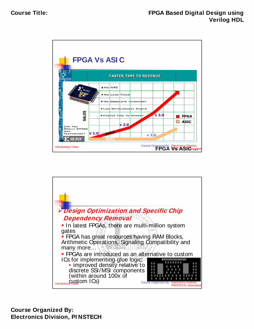
FPGA Vs ASIC
FPGA Vs ASIC …
Introductory Class Course Organized By: Electronics Division, PINSTECH, Islamabad
Design Optimization and Specific Chip Dependency Removal
FPGAs are introduced as an alternative to custom ICs for implementing glue logic:
• improved density relative todiscrete SSI/MSI components(within around 100x of custom ICs)
FPGA has great resources having RAM Blocks, Arithmetic Operations, Signaling Compatibility and many more…
In latest FPGAs, there are multi-million system gates

Course Title: FPGA Based Digital Design using Verilog HDL
Course Organized By: Electronics Division, PINSTECH
Introductory Class Course Organized By: Electronics Division, PINSTECH, Islamabad
System Integration
FPGA
Introductory Class Course Organized By: Electronics Division, PINSTECH, Islamabad
FPGA Technology
50M
2M
1M
500K
1998 1999 2000 2001 2002 2003 2004
4M
10M
SystemGates
FPGAs with2 million
system gateswere available in 1998 and . . . . . . FPGAs with
50 millionsystem gateswill be available in 2004
Moore’s Law: In 1965, Gordon Moore noted that the number of transistors on a chip doubled every 18 to 24 months. He made a prediction that semiconductor technology will double its effectiveness every 18 months.
Course Title: FPGA Based Digital Design using Verilog HDL
Course Organized By: Electronics Division, PINSTECH
Introductory Class Course Organized By: Electronics Division, PINSTECH, Islamabad
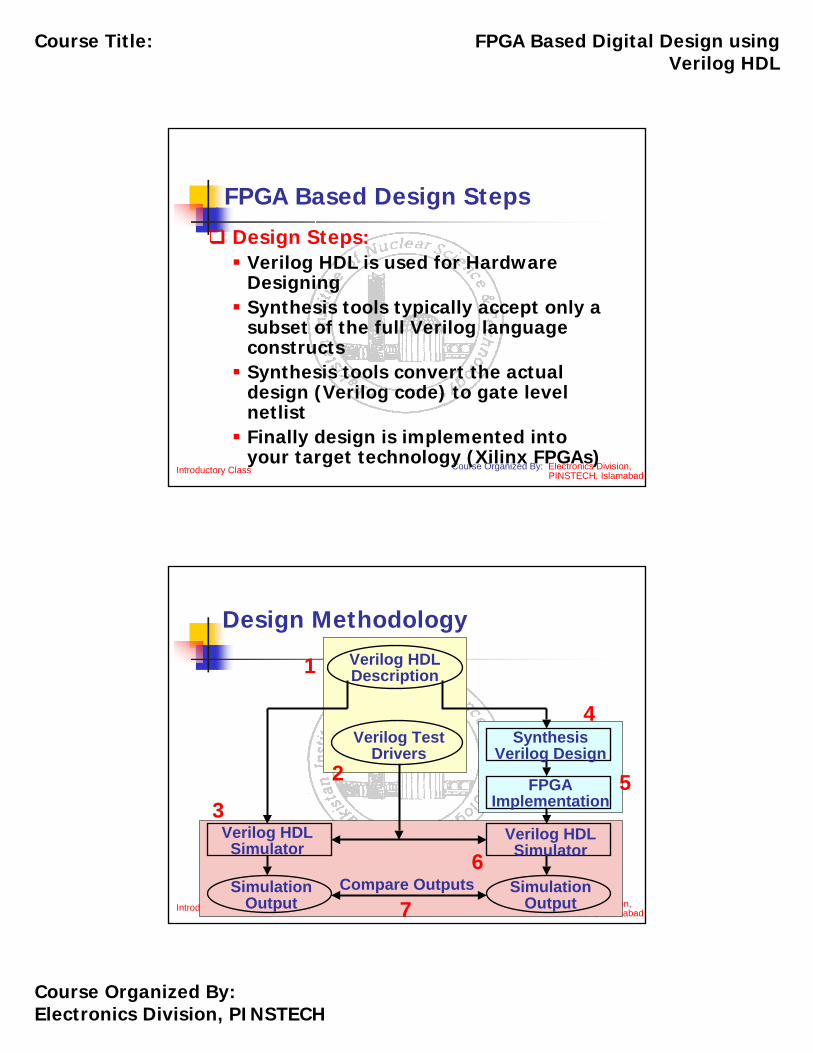
FPGA Based Design Steps
Design Steps:Verilog HDL is used for Hardware DesigningSynthesis tools typically accept only a subset of the full Verilog language constructsSynthesis tools convert the actual design (Verilog code) to gate level netlistFinally design is implemented into your target technology (Xilinx FPGAs)
Introductory Class Course Organized By: Electronics Division, PINSTECH, Islamabad
Design Methodology
1
2
3
4
5
6
7
Verilog HDL Description
Verilog Test Drivers
Verilog HDL Simulator
Synthesis Verilog Design
FPGA Implementation
Verilog HDL Simulator
Simulation Output
Simulation Output
Compare Outputs
Course Title: FPGA Based Digital Design using Verilog HDL
Course Organized By: Electronics Division, PINSTECH
Introductory Class Course Organized By: Electronics Division, PINSTECH, Islamabad
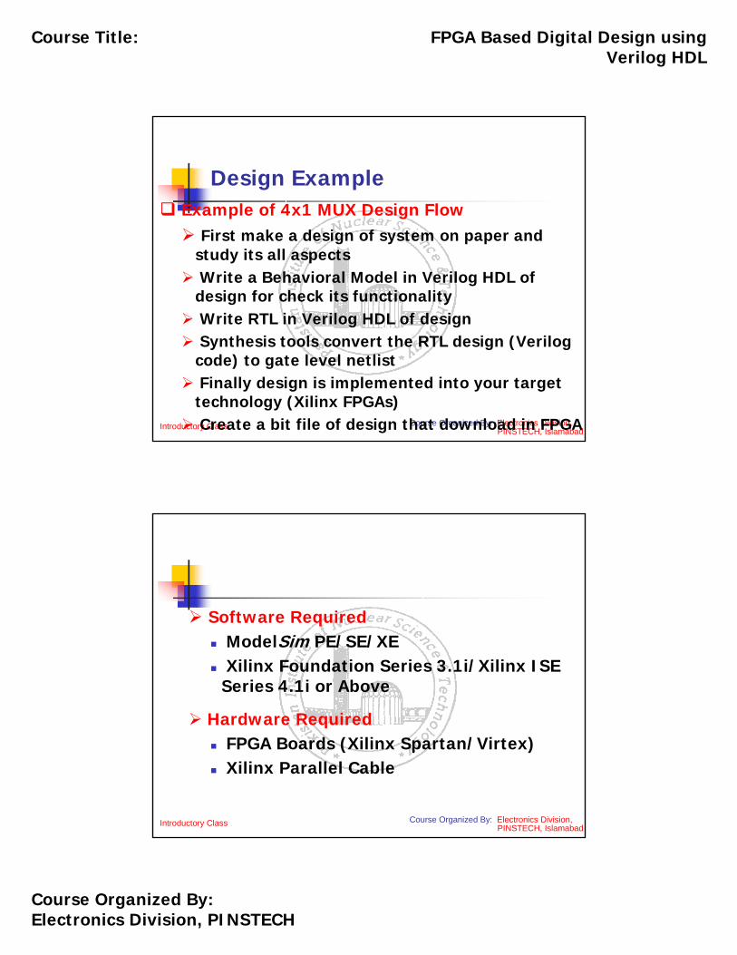
Design ExampleExample of 4x1 MUX Design Flow
First make a design of system on paper and study its all aspectsWrite a Behavioral Model in Verilog HDL of
design for check its functionalityWrite RTL in Verilog HDL of design Synthesis tools convert the RTL design (Verilog
code) to gate level netlistFinally design is implemented into your target
technology (Xilinx FPGAs)Create a bit file of design that download in FPGA
Introductory Class Course Organized By: Electronics Division, PINSTECH, Islamabad
Software RequiredModelSim PE/SE/XEXilinx Foundation Series 3.1i/Xilinx ISE Series 4.1i or Above
Hardware RequiredFPGA Boards (Xilinx Spartan/Virtex)Xilinx Parallel Cable

Course Title: FPGA Based Digital Design using Verilog HDL
Course Organized By: Electronics Division, PINSTECH
Introductory Class Course Organized By: Electronics Division, PINSTECH, Islamabad
First we define its input and outputs ports (in size, numbers…) and assign a unique name of each port. Hereinputs: in_0, in_1, in_2, in_3 and sel_0, sel_1output: out_data
(*These are all single bit)
in_0in_1in_2in_3
out_dataMUX4X1
Block Diagram of 1-bit 4x1 MUXsel_1 sel_0
Introductory Class Course Organized By: Electronics Division, PINSTECH, Islamabad
Design 1-bit 4x1 MUX in Verilog HDL

Course Title: FPGA Based Digital Design using Verilog HDL
Course Organized By: Electronics Division, PINSTECH
Introductory Class Course Organized By: Electronics Division, PINSTECH, Islamabad
Test Bench for Design
Introductory Class Course Organized By: Electronics Division, PINSTECH, Islamabad
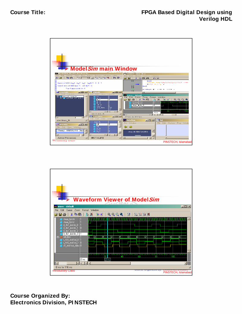
ModelSim main Window
Course Title: FPGA Based Digital Design using Verilog HDL
Course Organized By: Electronics Division, PINSTECH
Introductory Class Course Organized By: Electronics Division, PINSTECH, Islamabad
ModelSim main Window
Introductory Class Course Organized By: Electronics Division, PINSTECH, Islamabad
Waveform Viewer of ModelSim
Course Title: FPGA Based Digital Design using Verilog HDL
Course Organized By: Electronics Division, PINSTECH
Introductory Class Course Organized By: Electronics Division, PINSTECH, Islamabad
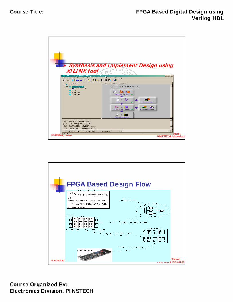
Synthesis and Implement Design using XILINX tool
Introductory Class Course Organized By: Electronics Division, PINSTECH, Islamabad
FPGA Based Design Flow
Course Title: FPGA Based Digital Design using Verilog HDL
Course Organized By: Electronics Division, PINSTECH
Introductory Class Course Organized By: Electronics Division, PINSTECH, Islamabad
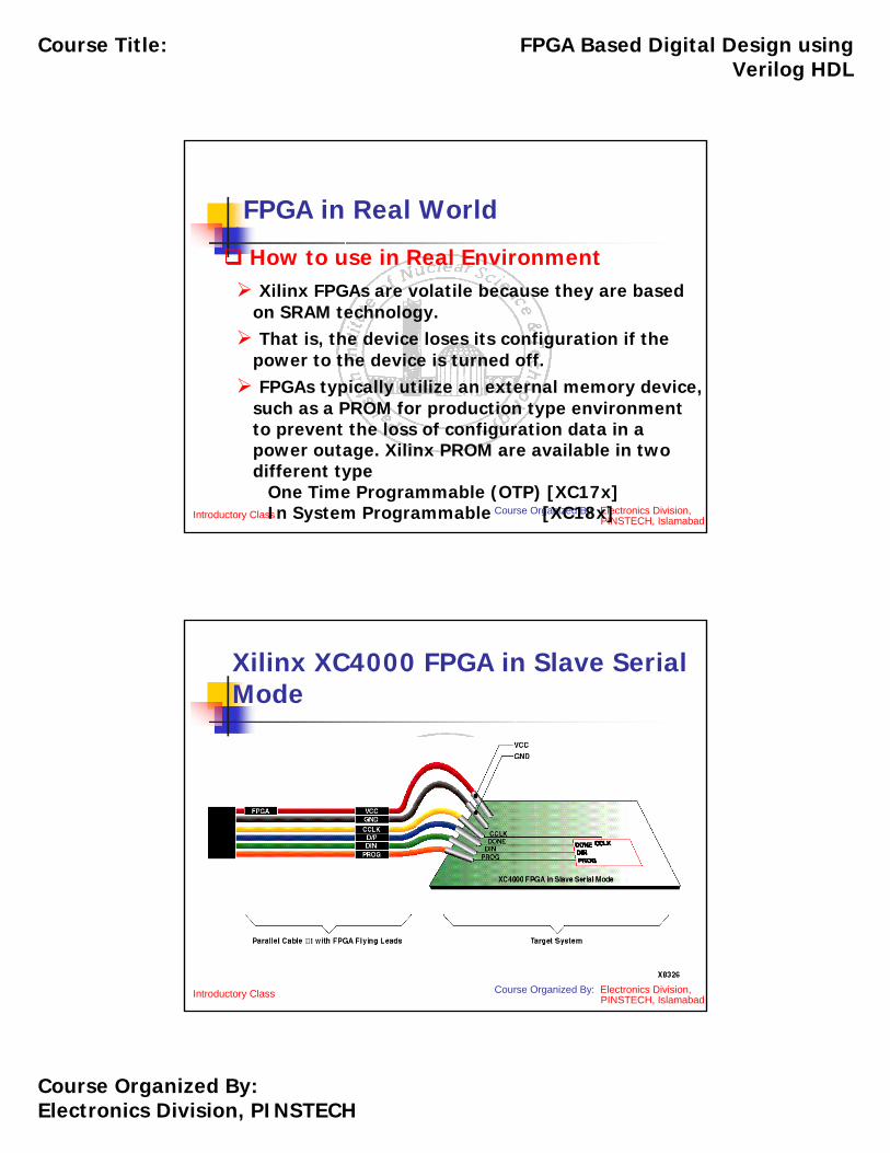
FPGA in Real World
How to use in Real EnvironmentXilinx FPGAs are volatile because they are based
on SRAM technology.That is, the device loses its configuration if the
power to the device is turned off.FPGAs typically utilize an external memory device,
such as a PROM for production type environment to prevent the loss of configuration data in a power outage. Xilinx PROM are available in two different type
One Time Programmable (OTP) [XC17x]In System Programmable [XC18x]
Introductory Class Course Organized By: Electronics Division, PINSTECH, Islamabad
Xilinx XC4000 FPGA in Slave Serial Mode

Course Title: FPGA Based Digital Design using Verilog HDL
Course Organized By: Electronics Division, PINSTECH
Introductory Class Course Organized By: Electronics Division, PINSTECH, Islamabad
Xilinx FPGA use with PROM
External Source
Select Mode
FPGAP R O M
JTAG Header
PCB
Introductory Class Course Organized By: Electronics Division, PINSTECH, Islamabad
FPGA Development kit
Xilinx Virtex-E Development Kit

Course Title: FPGA Based Digital Design using Verilog HDL
Course Organized By: Electronics Division, PINSTECH
Introductory Class Course Organized By: Electronics Division, PINSTECH, Islamabad
Motivation
System On Chip (SoC)SoC means you put the entire system on a single chipYour Analog and Digital Design on a single chipExample of any complex design that have Micro controller, Memories, Analog portion, DSP processor and algorithm on FPGAConcept is that put all above in a single chip
Introductory Class Course Organized By: Electronics Division, PINSTECH, Islamabad
New market of business in electronicsFor SoC you need the Core of every component i-e IP (Intellectual Property) of these coreYou can build your own IP…A group of two or three engineers
Course Title: FPGA Based Digital Design using Verilog HDL
Course Organized By: Electronics Division, PINSTECH
Introductory Class Course Organized By: Electronics Division, PINSTECH, Islamabad
Course Strategy
InformationInstructor
Irfan Faisal Mir (M.Sc Electronics)[email protected]
PrerequisiteDigital Logic DesignComputer Architecture ConceptProgramming Basics
Introductory Class Course Organized By: Electronics Division, PINSTECH, Islamabad
Course Duration:Two Weeks (Five days per week)
Total Lectures:Twenty (20) (Time: ≈ 1.5 hrs per lecture)
Total LABS:Twenty (20) (Time: ≈ 1.5 hrs per lab)
Course Title: FPGA Based Digital Design using Verilog HDL
Course Organized By: Electronics Division, PINSTECH
Introductory Class Course Organized By: Electronics Division, PINSTECH, Islamabad
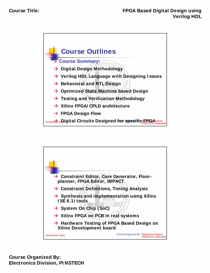
Course Summary:Digital Design Methodology
Verilog HDL Language with Designing Issues
Behavioral and RTL Design
Optimized State Machine based Design
Testing and Verification Methodology
Xilinx FPGA/CPLD architecture
FPGA Design Flow
Digital Circuits Designed for specific FPGA
Course Outlines
Introductory Class Course Organized By: Electronics Division, PINSTECH, Islamabad
Constraint Editor, Core Generator, Floor-planner, FPGA Editor, iMPACT
Constraint Definitions, Timing Analysis
Synthesis and implementation using Xilinx ISE 6.1i tools
System On Chip (SoC)
Xilinx FPGA on PCB in real systems
Hardware Testing of FPGA Based Design on Xilinx Development board