forty-9er assembly instruction manual - farrukhzia · · 2016-03-032 header-socket-10pin u3...
TRANSCRIPT

QS-03/16 QST in Depth - Purdum Page 1
Forty-9er Assembly Instruction Manual
by Dr. Jack Purdum, W8TEE; Farrukh Zia, K2ZIA; Dennis Kidder, W6DQ
This addendum presents additional assembly instructions that we made while assembling
the Forty-9er. It’s a fun little rig and you just can’t beat the price.
READ THROUGH THIS ENTIRE MANUAL BEFORE ASSEMBLING ANYTHING.
The order in which you do things can make it much easier to assemble the transceiver, or
more difficult if you use a different sequence for assembling the boards.
The instructions presented here are used in conjunction with the QST article for
modifying the Forty-9er. In addition to the normal kit assembly tools, we suggest you have a
flash light and magnifying glass.
We have also included the modifications necessary to the Forty-9er board to make it
easier to add the new LCD display and the DDS VFO. Adding the LCD display and the VFO
requires some parts be left off the original Forty-9er board and additional parts added onto it.
These changes are presented here, so you will know what not to solder onto the Forty-9er board
from the stock parts list you received when you bought your Forty-9er kit.
SN Parts needed for Forty-9er board modifications: Quantity
1 R5 replacement 10 k 1
2 D2 replacement 5.1V Zener diode 1
3 Inductor 22 µH 1
4 Disc ceramic capacitor 56 pF 1
5 Header Pins (single row 1x4) 1

QS-03/16 QST in Depth - Purdum Page 2
SN Parts needed for Nano DDS VFO: Identification / Code Schematic & PCB
Reference
Quantity
1 DDS VFO PCB PCB 1
2 Header-socket-10pin U3 socket 2
3 Header-socket-15pin U2 socket 2
4 Header-pins-2x4-white J1-A 1
5 Header-pins-2x4-yellow J1-B 1
6 Header-pins-2x4-blue J1-C 1
7 Header-pins-1x8-black U1,J2,J3 1
8 Volt-Reg-Mini-360 Circuit Module U1 1
9 Transistor-2N2222A Emitter-Base-Collector
(Front View)
Q1,Q2 2
10 Diode-1N4001 D1,D2,D3 3
11 Inductor-100uH Brown-Black-Brown-Silver L1 1
12 Capacitor-100nF-50V Ceramic-104 C1 thru C7 7
13 Capacitor-100uF-25V Electrolytic-100uF-25V C8 1
14 Resistor-TrimPot-10k Plastic-103 R1,R8 2
15 Resistor-220-1/4W Red-Red-Brown-Gold R2 1
16 Resistor-1k5-1/4W Brown-Green-Red-Gold R3 1
17 Resistor-12k-1/4W Brown-Red-Orange-Gold R4 1
18 Resistor-470-1/4W Yellow-Violet-Brown-Gold R5a,R5b 2
19 Resistor-470-1/4W Yellow-Violet-Brown-Gold R6a,R6b 2
20 Resistor-20k-1/4W Red-Black-Orange-Gold R7 1
21 Arduino Nano Module 1
22 AD9850 DDS Module 1
23 16x2 characters LCD with I2C interface
1
24 Rotary Encoder with integrated switch
1
25 Dupont jumper wires (F-F), 8” length 10
26 RG174 coax cable, 6” length (optional, for connecting DDS VFO output to Forty-9er and Forty-9er output to antenna BNC connector)
2

QS-03/16 QST in Depth - Purdum Page 3
Header pins are built from standard header pins available from www.ebay.com. Search for,
“10PCS 40Pin 2.54mm Single Row Straight Male Pin Header Strip PBC Arduino”.
The following sequence allows the board to be built and soldered in layers, starting with the
lower profile components and then gradually installing components with more height.
Sequence of parts placement for soldering on the 40-9er PCB.
1. IC sockets
2. Ceramic capacitors (0.1 F)
3. Ceramic capacitors (all others)
4. Electrolytic capacitors (1 F and 10 F)
5. Resistors
6. Header pins in place of Y2, Jumper across W1
7. Diodes
8. TO92 transistors and U1 (VR)
9. Electrolytic capacitors (100 F)
10. Inductors
11. Jacks and Connectors
12. Power Transistor
Figure A1 shows the original Forty-9er schematic as received with the kit. For the most part, the
modifications made apply to the crystal-controlled filter and oscillator supplied with the kit.

QS-03/16 QST in Depth - Purdum Page 4
Figure – A1 Original Forty-9er Schematic.
QS-03/16 QST in Depth - Purdum Page 5
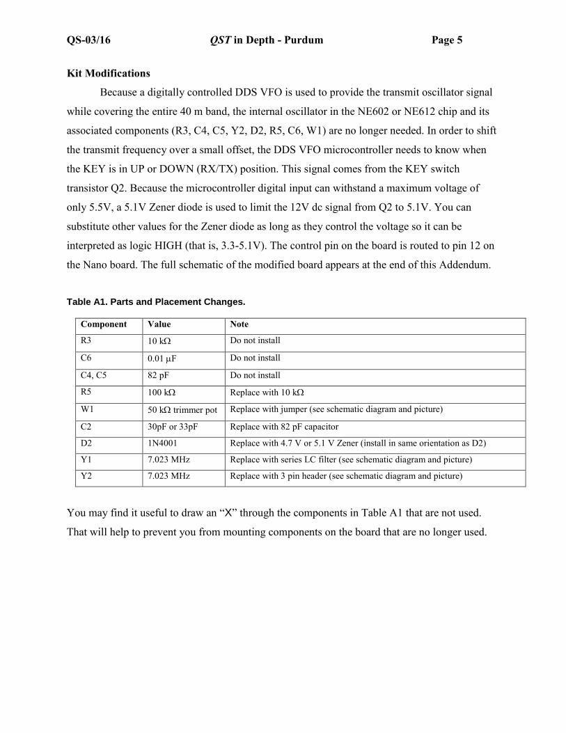
Kit Modifications
Because a digitally controlled DDS VFO is used to provide the transmit oscillator signal
while covering the entire 40 m band, the internal oscillator in the NE602 or NE612 chip and its
associated components (R3, C4, C5, Y2, D2, R5, C6, W1) are no longer needed. In order to shift
the transmit frequency over a small offset, the DDS VFO microcontroller needs to know when
the KEY is in UP or DOWN (RX/TX) position. This signal comes from the KEY switch
transistor Q2. Because the microcontroller digital input can withstand a maximum voltage of
only 5.5V, a 5.1V Zener diode is used to limit the 12V dc signal from Q2 to 5.1V. You can
substitute other values for the Zener diode as long as they control the voltage so it can be
interpreted as logic HIGH (that is, 3.3-5.1V). The control pin on the board is routed to pin 12 on
the Nano board. The full schematic of the modified board appears at the end of this Addendum.
Table A1. Parts and Placement Changes.
Component Value Note
R3 10 k Do not install
C6 0.01 F Do not install
C4, C5 82 pF Do not install
R5 100 k Replace with 10 k
W1 50 k trimmer pot Replace with jumper (see schematic diagram and picture)
C2 30pF or 33pF Replace with 82 pF capacitor
D2 1N4001 Replace with 4.7 V or 5.1 V Zener (install in same orientation as D2)
Y1 7.023 MHz Replace with series LC filter (see schematic diagram and picture)
Y2 7.023 MHz Replace with 3 pin header (see schematic diagram and picture)
You may find it useful to draw an “X” through the components in Table A1 that are not used.
That will help to prevent you from mounting components on the board that are no longer used.

QS-03/16 QST in Depth - Purdum Page 6
Figure A2 – The modifications for the Forty-9er board.
The modifications shown in Figure A2 involve removing the two (receive filter and
transmit oscillator) crystals and modifying the circuit around the crystal locations. Also note that
original schematic shows C21 and C2 values as 33pF but the actual kits contain 30 pF capacitors
as shown in modification schematic. Pin J5 carries receive frequency offset signal to Nano. J6
carries the DDS VFO output to the NE602 or NE612 (for receiver demodulation) and to transmit
pre-amp (via C10). Note; header pins labeled J5 and J6 and circled in red in Figure A2 are new
pins we added to the Forty-9er board. (These show up as yellow pins in Figure A4.)
Receive filter modification:
In the original circuit, C21, Y1, C2 form a narrow band receive crystal filter. This is
replaced with a wider band LC filter which covers the entire 40 m band from 7.000 to
7.300 MHz. We used LT-Spice simulations to model the receive filter response. Model and
response are shown in Figure A3.

QS-03/16 QST in Depth - Purdum Page 7
We used C21 (30 pF) and C2 (82 pF) for the modification because they become unused
parts already included in the kit. In Figure A3 left, C15 (8 pF) in the design is the combined
capacitance of limiter diodes D1 and D5 (4 pF each, from 1N4148 datasheet). Cin and Rin are
input capacitance and impedance of NE602 mixer input pin 1 (from NE602 data sheet).
Figure A3 – Filter model (top) and response (bottom).

QS-03/16 QST in Depth - Purdum Page 8
Figures – A4 Modifications made to the board.
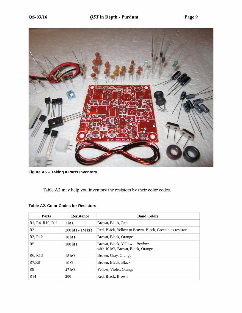
Parts Inventory and Prep Work
You must do a parts inventory. As it turned out, all of the kits we ordered had extra parts
shipped with the kits, although one kit was short on the 0.1 F capacitor count. While more is
better than having missing parts, it can be disconcerting to finish building something only to
discover anywhere from 3 to 5 parts left in the parts bin.
Our preferred inventory method is to use a large chunk of Styrofoam into which we can
punch the parts as we check them off the list. It’s probably a bad idea to stick static-sensitive
components, like ICs and transistors, into the foam. Just leave those to the side of the Styrofoam
sheet. Line up parts as you do the inventory. For example, if there are four 1 k resistors on the
parts list, line them up one behind the other in the Styrofoam. That way, they are easy to count
during the inventory and easy to find during construction. Heathkit suggested putting the
components into the “holes” left when you cut out a piece of cardboard and sit it upright on edge.
Use whatever you think best.
QS-03/16 QST in Depth - Purdum Page 9
Figure A5 – Taking a Parts Inventory.
Table A2 may help you inventory the resistors by their color codes.
Table A2. Color Codes for Resistors
Parts Resistance Band Colors
R1, R4, R10, R11 1 k Brown, Black, Red
R2 200 k - 1M k Red, Black, Yellow to Brown, Black, Green bias resistor
R3, R12 10 k Brown, Black, Orange
R5 100 k Brown, Black, Yellow – Replace
with 10 k, Brown, Black, Orange
R6, R13 18 k Brown, Gray, Orange
R7,R8 10 Brown, Black, Black
R9 47 k Yellow, Violet, Orange
R14 200 Red, Black, Brown
QS-03/16 QST in Depth - Purdum Page 10
The capacitors are pretty clearly marked, but you may need to use the magnifying glass,
and perhaps a flashlight, to read the numbers on them. The relationship between the number on a
cap and its value, see the EIA Capacitor Values or go search www.elecraft.com/Apps/caps.htm
for some sample capacitance values relative to their numbers.
The electrolytic capacitors are easily identified, just pay attention to their polarity when
you install them. Most have a thick white band on the casing with a minus sign on it to identify
the negative lead. The silk screen has a “shaded half circle” painted on the negative lead. On our
boards, C19 is silk screen on the board as an electrolytic, but is actually a disc cap now. (It's
correct on the parts list.)
Diodes and Zener diodes have a band around their cathode (negative) lead. The only
other part that might be confusing are the inductors. They look like a fat resistors, but have a
greenish base color versus the tan or blue base color for resistors. (You can see the inductor
sticking upright in the upper-right corner of Figure A5.)
Toroid Winding
You must wind inductor toroids L3 and L4 yourself according to Table A3. It’s easy.
Table A3. Inductor windings
Part Turns Core
L3 11 FT37-43 (Black core)
L4 16 T37-2 (Red core)
To make each toroid, first cut the supplied enamel wire approximately in half. Holding about 1
inch extra from the end, push the other end over the top of the core, then back through the middle
and then back to the top of the core. That loop counts as one turn. Keep repeating until you have
completed the required number of turns according to Table A3. After you’re done, fan the turns
so they are more-or-less evenly distributed around the core. Take a sharp tool (or light
sandpaper) and carefully scrape away the enamel from both leads up to the bottom of the core.
Alternatively you can use the tip of a hot soldering iron to melt the enamel away, which removes
the risk of nicking the wire. Either way helps make a good solder joint with the PCB. We always

QS-03/16 QST in Depth - Purdum Page 11
perform a continuity test with a DMM after we’ve soldered them in place just to make sure we
have a good connection.
Do not mount the toroids on the board yet.
Pre-Assembly Considerations
You can put the parts on the PCB any way you wish, but we always follow a pattern
when assembling a kit with “skimpy” instructions. First, there are quite a few parts to fit on the
small area of the Forty-9er PBC. It’s a pretty dense board, especially for fat-fingered old people.
Also, there is no apparent organization to the positioning of the parts. That is, R1 might be at the
northwest corner of the board while R2 is at the southeast corner. The printed instructions have a
copy of the board’s silk screen and we found that invaluable in locating where a part was to be
placed. You might find it helpful to use a yellow highlighter pen to color each component on the
schematic as it is added. That makes it easier to find the location of the remaining components.
Figure A6. The Original Forty-9er Circuit from Vendor.

QS-03/16 QST in Depth - Purdum Page 12
Figure A6 shows the original circuit as it comes from the seller, as compared to the
modifications shown in Figure A2. Because we are adding an LCD display and DDS VFO to the
rig, the original circuit needs several modifications. Most of the modifications are focused on the
NE602 double-balanced mixer U2 in Figure A6. Both crystals Y1 and Y2 are removed from the
circuit to convert the circuit from a crystal-controller to oscillator to a VFO.
Figure A7. Schematic of Modifications to Forty-9er board, shown earlier as Figure A2.
Before You Solder Anything on the Forty-9er Board...
We learned the hard way that assembly is easier if you follow a specific sequence. We
are repeating Figure A2 here as Figure A7 to make it easier to reference the schematic during the
discussion.
Replace the input crystal receive filter (Y1) of Figure A6 with an LC tuned circuit shown
in Figure A7 consisting of a 22 H inductor (Lx) and a 56 pF capacitor (Cx). Place this filter
near diodes D1-D5 on the board, in the lower-right corner of the PCB. (You can see this clearly

QS-03/16 QST in Depth - Purdum Page 13
in Figure A9.) The new oscillator circuit is placed near the location of Y2 on the circuit board.
Details for adding the new components is given below.
We used (yellow) header pins to make the board connections, since this makes it easy to
use Dupont jumper wires for connections between the Forty-9er and Nano/VFO boards. If you
don’t have any header pins, you could make your own pins using #20 or #22 AWG wire instead.
As a last resort, you could solder wires directly between the two boards, but this makes it harder
to work with the two boards during construction, so we don’t recommend direct wiring.
Figure A8. Soldering the middle pin of the 3 pin header at location Y2.

QS-03/16 QST in Depth - Purdum Page 14
Figure A9. The narrow pass receiver filter components in place.
Forty-9er Board Modifications
We suggest this sequence of steps:
Take one of the 8 pin IC sockets and, using a pair of needle nose pliers, push on pin 7 from the
bottom upwards until it pops out the top of the socket. As you can see from Figure A7, we don't
use pin 7 of the NE602, but we are going to use some PCB connections that were tied to pin 7 for
other purposes. Popping out the pin 7 contact assures us that we don’t use that pin of the NE602.

QS-03/16 QST in Depth - Purdum Page 15
Cut a group of 3 pins from a row of standard header pins and, using either a snipping tool
or toenail clippers. The “short end” of the pins fit into the Forty-9er board, while the “long end”
of the pins will eventually be used to connect Dupont wires to the Nano/VFO board. Bend the
middle short pin of the three-pin header to form a right angle. Place the three-pin header into the
two holes that are marked Y2 on the board with the bent middle pin pointing towards CP3. The
bent pin should almost cover a hole that’s between CP3 and the three-pin header. This middle
pin is the ground connection for the J2 and J1 connections seen in Figure A7. Solder the middle
pin to the hole that is between CP3 and U1. Flip the board over and solder the remaining two
pins to the board. See Figure A8 for the details.
In Figure A8, you can see the silk screen for C10 to the right of CP3. You can also see
the trace running from C10 to pin 7 of the NE602 chip U2 in Figure A7. We no longer use the
oscillator components of the original circuit or pin 7 of U2. You can also see that the other lead
of C10 connects to the base of Q6, which is the transmit pre-amp. According to Table A1 we no
longer need C4 or C5 in the circuit, so with a little care, we can use their mounting holes in our
modified circuit.
In Figure A8, note how the trace from our new J2 header pin passes to the right side of
C5 and then to pin 6 of U2. If we don’t trim the lead from C10 but instead route it on the under-
side of the PCB and through the right-side hole of C5, we complete the circuit between J2, U2,
and C10 as shown in Figure A7. Because we removed the pin 7 contact in Step 1 and R3 and C4
are no longer in the circuit, the existing trace from C10 to pin 7 no longer matters.
Mount C10 on the circuit board and solder it in place, but do not trim the lead that goes to
the trace that currently runs to pin 7 of U2. Instead, slip some insulation on the lead and route it
to the mounting hole on the right side of C5 when viewed as shown in Figure A6. The path of the
lead from C10 to the right side mounting hole of C5 is shown as a green line in Figure A8, but is
on the under-side of the PCB. The 82 pF capacitor we received for C10 has pretty short leads and
barely spans the distance to the C5 mounting hole. If this is a problem for you, push a bare wire
through the correct C5 mounting hole and solder the wire in place. Trim off the excess from the
top of the board. Now flip the board over and connect the bare wire to the lead coming from C10
and solder, thus completing the green line connection between C5 and C10. Cover the leads with
electrician’s tape or use heat-shrink tubing before connecting the two leads, and shrink it after

QS-03/16 QST in Depth - Purdum Page 16
soldering. We were able to slip some Teflon tubing over the C10 lead and bend it to touch the C5
mounting hole and solder it in place.
Next, replace the narrow band receive filter that uses crystal Y1 with an LC filter built
from Cx and Lx in Figure A7. We change the value of capacitor C2 from 33 pF to 82 pF. This is
not a problem since we no longer need C4 or C5, both of which are 82 pF. Place one end of
inductor Lx, 22 H, into the mounting hole for Y1 and soldered it in place. Twist the other end
of Lx together with one lead from capacitor Cx, 56 pF, and solder the two leads together. Mount
the free end of Cx into the remaining unused hole of Y1 and solder it in place. Figure A9 shows
the LC filter soldered in place.
Mounted C2 (Figure A9) making sure to replace the original value of 33 pF with the new
value of 82 pF.
Replace D2 with a 5.1 V Zener diode and solder it in place. We used a 1N4733A, which
is a 1 A diode. We found them locally at 10 for $1.25 at, www.debcoelectronics.com. Search for
“1N4733”. Make sure you orient the diode so the cathode band mounts in the hole closest to the
J2 header pins. Save one of the trimmed diode leads for step #8. D2 ensures that the voltage on
the J1 header pin doesn’t exceed 5.1 V even though there is 12 V on the emitter of Q2. By
reading the emitter of Q2, J1 supplies a signal to pin D12 on the Nano to sense when the
transmitter is keyed.
Replace the original R5 (100 k) with a 10 k resistor and solder it in place. As you can
see in Table A1, R3 is a 10 k which is no longer needed, so you can use it for R5.
Use the trimmed lead from step #7 to make a jumper that spans W1 from its wiper to the
emitter of Q2. The modifications for steps 6-8 are shown in Figure A10.
This completes the modifications that you need to make to the Forty-9er board. It
wouldn't hurt to examine your work and make continuity checks with an ohmmeter to make sure
you have things wired correctly.

QS-03/16 QST in Depth - Purdum Page 17
Figure A10. Oscillator modifications.
Forty-9er Component Completion
At this point, you can place the remaining components on the Forty-9er board. Make sure
you follow the omission/modification details presented in Table A1, as there are components in
the kit that are no longer needed.
The sequence from this point is up to you. However, we find it easiest to mount the IC
sockets first. Since we want the IC sockets to sit flat on the board, we Scotch tape them to the

QS-03/16 QST in Depth - Purdum Page 18
board and then flip the board and solder them in place. Next, we place the remaining diodes on
the board. Since these are heat sensitive, so solder only one lead on each diode at a time and
move to the next one. After you’ve soldered one lead of each diode, go back and solder the
remaining free lead. This gives the diode a chance to cool down before you solder the second
lead is soldered. We do the same thing for each transistor lead, soldering one lead, move to the
next, and so on, then returning to solder the second lead of the first transistor. Again, this gives
the transistor a chance to cool a bit before soldering the next lead.
Next, we place and solder all of the resistors, then the (non-electrolytic) capacitors,
followed by the electrolytic capacitors. Solder the large components (toroids, speaker/key
connectors) last.
If you think you may add software for an electronic keyer, the Forty-9er board does NOT
wire the key connector for keyer use. It assumes a straight key. You will need to route a wire
from the key connector’s ring pin and tie it to an unused pin on the Nano that you want to use for
the keyer. Arduino Projects for Amateur Radio has details for such a keyer, or just search with
your browser for “Arduino Morse Code keyer”.
Cold Solder Joints
A cold solder joint (CSJ) is the bane of kit builders. A CSJ is a soldered connection that
does not make a good electrical contact between two or more components. Often you can spot a
CSJ by looking at the connection with a magnifying glass. The joint will look “grainy”, with a
crystalline appearance rather than a smooth shiny surface. Sometimes you can see that the solder
has not flowed evenly around a lead, causing a CSJ. We always “strum” a component lead before
we trim it off. If the connection is good, the lead will give an almost musical note when you
strum it with your fingernail. If you hear a thud instead of a note, re-solder the connection.
The Nano DDS VFO Board
Figure A11 shows the schematic for the VFO/Nano board. Near the upper-left of Figure
A11 is a large, 24 pin header labeled J1 that provides the power and control logic for the board.
This 24 pin header is nothing more than two 12 pin header blocks mounted next to each other,
similar to the header built using the “yellow” pins of J5 and J6. Vin is 12 to 13.8 V at 1 A
supplied from an external power supply. L1 and C4 decouple the buffer Q1-Q2 from the 12V

QS-03/16 QST in Depth - Purdum Page 19
power supply. R6 is probably sufficient to provide decoupling with C4, but L1 provides an extra
measure of providing a high impedance source at RF.
Figure A11. The Nano/VFO Schematic.
C1-C7 — capacitor, 0.1 µF
C8 — electrolytic capacitor, 100 µF 25 V
D1,D2,D3 — diode,1N4001
J1 — 24 pin header*
J2 — 2 pin header*
J3 — 2 pin header*
L1 — Inductor, 100 µH (www.vetco.net)
Q1,Q2 — NPN transistor, 2N3904 or 2N2222A
R1,R8 — trimmer potentiometer, 10 kΩ
R2 — resistor, 220 Ω
R3 — resistor, 1.5 kΩ
R4 — resistor, 12 kΩ
R5,R6 — resistor, 220 Ω, 1/2W
R7 — resistor, 20 kΩ
U1 — Mini-360 Adjustable Buck Regulator
(www.ebay.com)
U2 — Arduino Nano R3
U3 — Direct Digital Synthesizer, AD9850.
S1 – Rotary encoder with integrated push
switch (www.ebay.com)
LCD – 16x2 character LCD with I2C interface
(www.ebay.com)
All resistors are 1/4W unless otherwise noted.
*Header pins J1, J2 and J3 are built from standard header pin strips available from
www.ebay.com. Search for, “10PCS 40Pin 2.54mm Single Row Straight Male Pin Header Strip PBC
Ardunio”.
QS-03/16 QST in Depth - Purdum Page 20
Note that we refer to header pin connectors J1, J2, and J3 in this section of the manual.
Keep in mind that we are now building the Nano/VFO board (see Figure A12), which is different
from the Forty-9er board which has it's own set of connectors J1-J4. Pretty much anyone who
can fog a mirror won't confuse the two, but we thought we'd mention it just to make sure.
The Nano/VFO board may be viewed as a “stand alone” VFO for rigs other than the
Forty-9er. Many modern QRP rigs require a rather modest peak-to-peak voltage from the VFO.
For example, we used a VFO with a similar design for the MFJ Cub and CRK lines of
transceivers. While the filter network would need some modifications for other bands, the VFO
is capable of 160 – 10 m operation. The output at J2 in Figure A11 can be used for rigs that don’t
need a large peak-to-peak voltage. Some older rigs, including the Forty-9er, need a larger signal
to bring the rig to its full output power. J3 provides up to 4V peak-to-peak via a small buffer
amplifier on the board. You can adjust the output voltage with R1. The output from J3 in Figure
A11 becomes the input to J6 in Figure A7.
Note that pin 24 on the J1 header in Figure A11 is tied to J5 in Figure A7. That is, the
keyed control signal from Q2 via the 5.1 V Zener diode on the Forty-9er board becomes the
control signal fed to pin D12 on the Nano/VFO board. This signal is used by the VFO control
software.
The I2C bus is used to route display output to the 2x16 LCD display. The I2C bus
simplifies the display connections because only 4 wires are required (SDA, SCL, GND, and 5V).
These I/O pins are pins 16, 14, 12, and 10 respectively on the J1 header. Dupont wires connect
from those pins to the appropriate pins on the LCD display.
Pin 17 (D4) on J1 is tied to the encoder’s center switch pin, while the rotary encoder
clock and data pins are tied to pins 18 (D2) and 22 (D3) on J1. For the Nano, D2 and D3 are the
pins used for external interrupts. The interrupts fire whenever the user rotates the encoder shaft.
Interpreting the pulse train from the encoder allows the software to determine whether the user is
tuning up or down the band.
Resistors R7 and R8 on the Nano/VFO board form a voltage divider circuit across the
12V power supply input. The output of this voltage divider is fed into analog input A7 of the
Nano. This arrangement will be used in a future revision of the control program to measure and
display the power supply voltage especially when the rig is powered by a 12V battery for
portable operation.

QS-03/16 QST in Depth - Purdum Page 21
Figure A12. Nano/VFO PCB.
Figure A12 shows the Nano/VFO PCB. Most of the discrete components mount flush to
the PCB and are located under the Nano/VFO boards. Note the 24-pin header on the lower left of
Figure A12, and the output header towards the right corner. For the output header, the right-most
two pins in Figure A12 form J3 in Figure A11 and the left-most two pins are J2. Use J3 with the
Forty-9er. The unpopulated as well as populated board can be seen in Figure A13.
After the Nano DDS VFO board is fully populated but BEFORE the Nano and DDS modules
are plugged into their socket headers, the output of the Mini-360 adjustable buck regulator

QS-03/16 QST in Depth - Purdum Page 22
must be adjusted to 5.0V. For this adjustment, connect 12V power to J1 pins 2 and 4, connect
DMM probes to the 5V and G (Ground) pads on the side of Nano/VFO PCB (see Figure A12)
and slowly rotate the tiny round trimmer potentiometer on the Mini-360 module with an
insulated jeweler’s Philips screw driver until you measure exactly 5.0 V on the DMM.
Figure A13. An unpopulated Nano/VFO PCB next to a populated PCB.
12V power for the Forty-9er is taken from pins 1 and 3 of the J1 header on the
Nano/VFO board. Most of the parts seen on the silkscreen are mounted under the Nano and
AD9850 boards as seen in Figures A12 and A13. At the last minute, we did add an On/Off
switch between the external power supply and the header, although this is not shown in the
schematics.
Figure A14 shows the populated Forty-9er board (before mounting the IC's). Note the
missing “tooth” for pin 7 on the socket for the NE602/612 chip, U2. When you mount the boards
in the case of your choice, just “snug” the mounting bolts, as over-tightening could crack the
PCB.

QS-03/16 QST in Depth - Purdum Page 23
Figure A14. The Populated Forty-9er Board, less the ICs.
Testing
There’s really not much you need to test. The first thing, with a magnifying glass, scan
the board for solder bridges or perhaps a piece of a wire that may have stuck to the board. Next,
perform a continuity test on the positive lead of the power connectors to ground for both boards.
If this shows no resistance, start looking for a solder bridge or some other form of short.
If everything looks normal, plug in a pair of headphones into the speaker jack, connect a
40 m antenna to J4, and apply power to J1 on the Nano/VFO board. After the sign on splash
screen, you should hear “white noise” in the headphones. If not, recheck your connections. If you
do hear the white noise but no CW signals, turn the VFO knob again. You should hear the
frequency shift and perhaps hear a CW signal. If not, recheck your wiring.

QS-03/16 QST in Depth - Purdum Page 24
If everything is going well, connect a key into the key input jack. If you can, turn on
another rig and tune to the displayed Forty-9er frequency, and press the key. You should hear a
note coming from your earphones (the sidetone from the Forty-9er) as well as from the second
receiver. You may have to tune up or down a few kilohertz to find your signal. Note the
frequency and adjust your VFO offset via software as described in the article.
Done!
You are now done, except for finding an enclosure for the rig. While a metal enclosure
would be best, we used a plastic acrylic enclosure from www.usacrylic.com.
We hope you found these additional instructions helpful.
PC Board Availability
We have a limited number of PCBs for the Nano/VFO board, which makes things a little
easier to assemble. Please visit www.farrukhzia.com/k2zia or email Farrukh at [email protected]
before ordering a board to make sure we still have one available at a cost of $6.95. The board is
approximately 2 inch by 2 inch and is red to match the Forty-9er board (Figure A13). If you
would like to purchase a board, send a check or money order to,
Farrukh Zia (K2ZIA)
799 Carpenter Rd
North Brunswick, NJ 08902, USA

QS-03/16 QST in Depth - Purdum Page 25