focused ion beam / focused electron beam nt ii - 2007€¢ theory based on quantum mechanical...
TRANSCRIPT
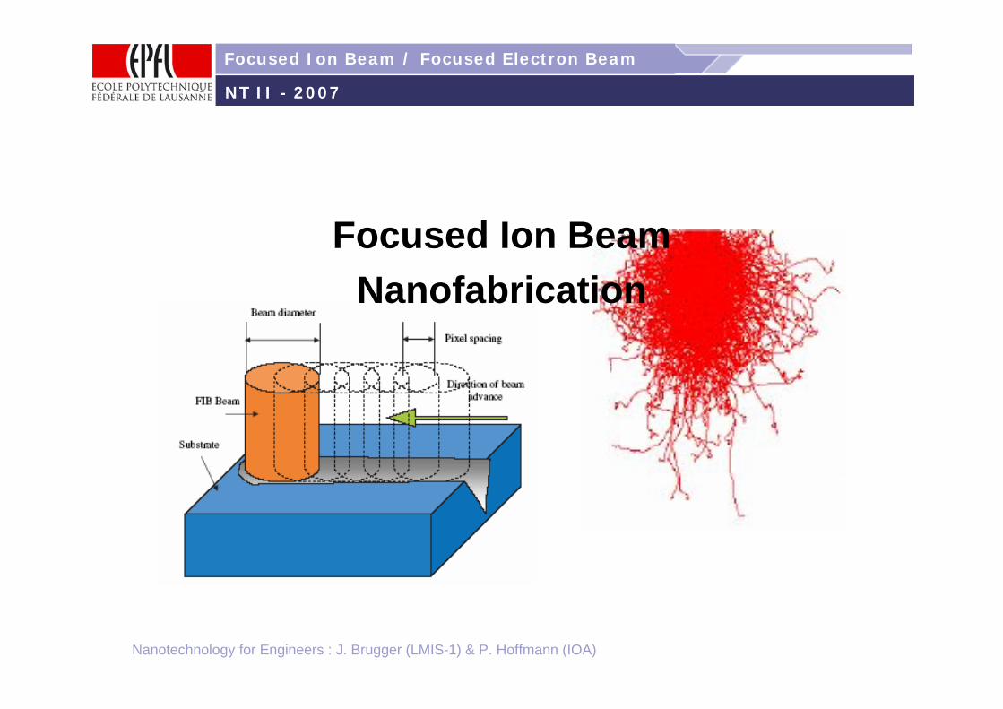
Nanotechnology for Engineers : J. Brugger (LMIS-1) & P. Hoffmann (IOA)
Focused Ion Beam / Focused Electron Beam
Focused Ion BeamNanofabrication
NT II - 2007
2
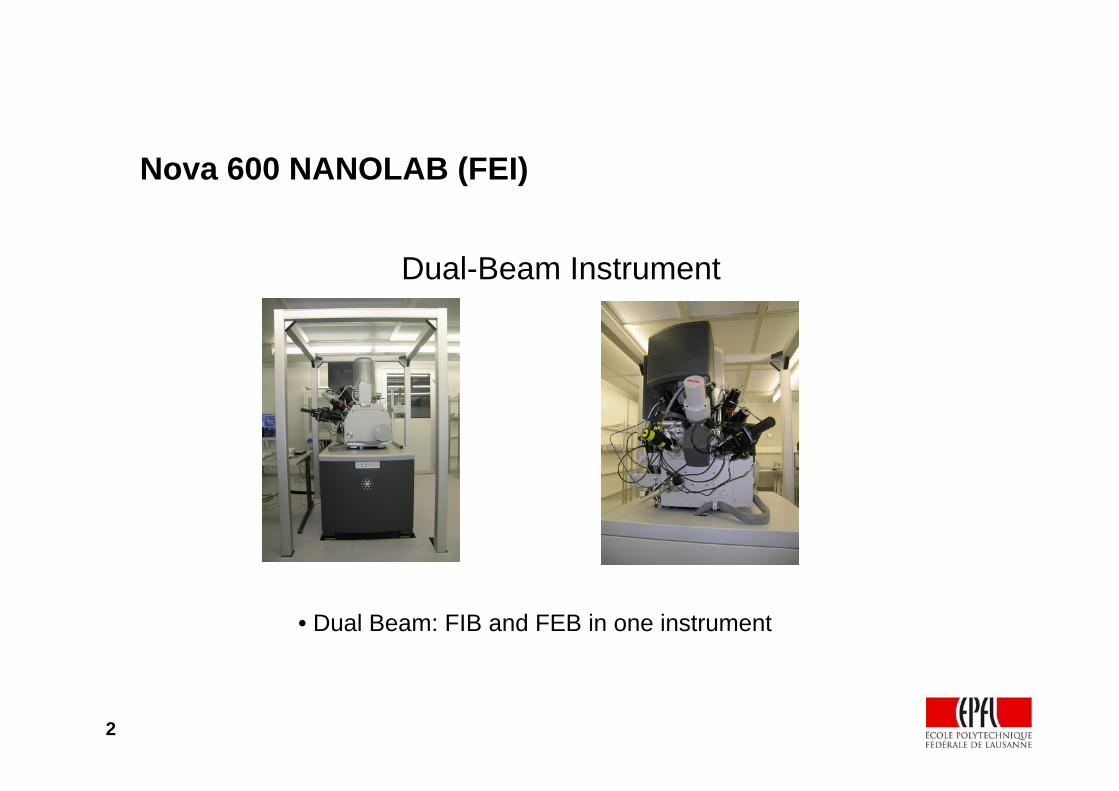
Nova 600 NANOLAB (FEI)
Dual-Beam Instrument
• Dual Beam: FIB and FEB in one instrument
3
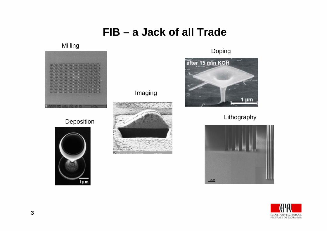
FIB – a Jack of all TradeMilling
Imaging
DepositionLithography
Doping
4
Table of Contents
IntroductionIon SourceIon OpticsIon-Solid InteractionMillingImagingApplications
5
Introduction
• Field emission reported the first time by R W Wood in 1897 (electrons)
• Theory based on quantum mechanical tunnelling (Fowler and Nordheim1928)
• Field Ion Microscope (FIM) introduced in the 50’s. For the first time atomic resolution has been achieved. (Müller 1951)
• Field ionisation based FIB were first developed in early 70’s.
6
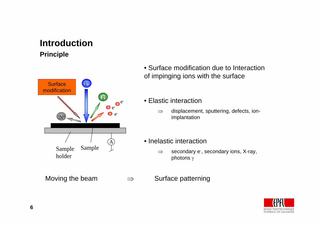
IntroductionPrinciple
I+
e-N0
e-e-I+
SampleA
Sampleholder
Surface modification
• Surface modification due to Interaction of impinging ions with the surface
• Elastic interaction⇒ displacement, sputtering, defects, ion-
implantation
• Inelastic interaction⇒ secondary e-, secondary ions, X-ray,
photons γ
Moving the beam ⇒ Surface patterning
7
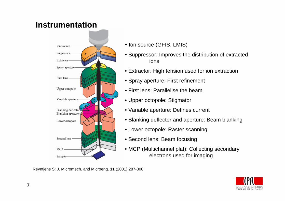
Instrumentation
• Ion source (GFIS, LMIS)
• Suppressor: Improves the distribution of extracted ions
• Extractor: High tension used for ion extraction
• Spray aperture: First refinement
• First lens: Parallelise the beam
• Upper octopole: Stigmator
• Variable aperture: Defines current
• Blanking deflector and aperture: Beam blanking
• Lower octopole: Raster scanning
• Second lens: Beam focusing
• MCP (Multichannel plat): Collecting secondary electrons used for imaging
Reyntjens S: J. Micromech. and Microeng. 11 (2001) 287-300
8
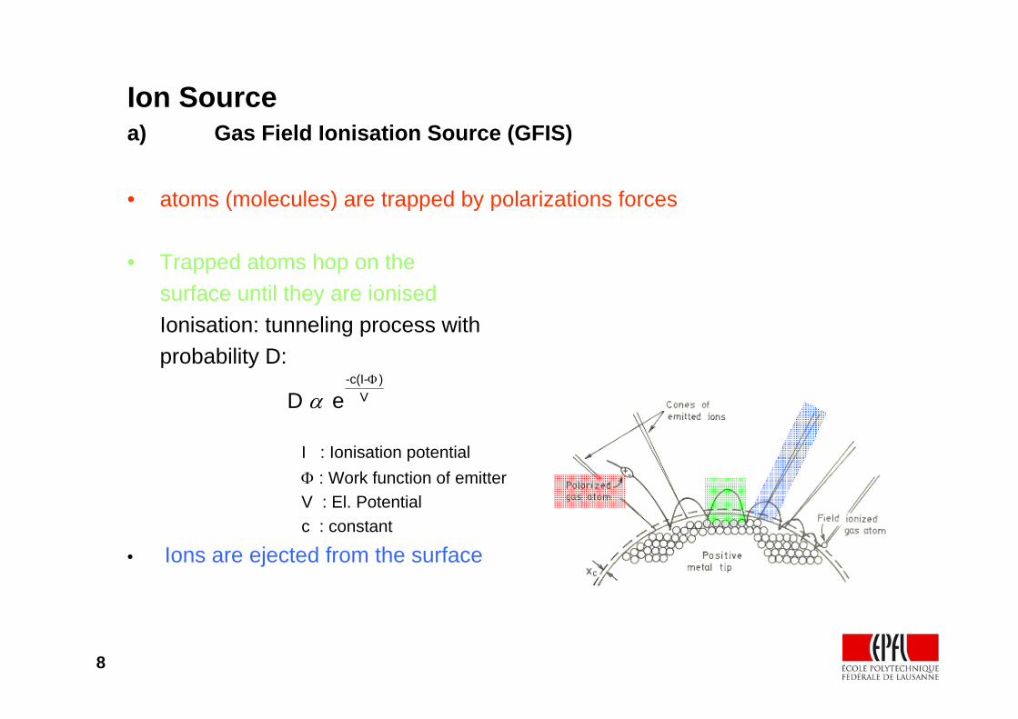
Ion Sourcea) Gas Field Ionisation Source (GFIS)
• atoms (molecules) are trapped by polarizations forces
• Trapped atoms hop on the surface until they are ionisedIonisation: tunneling process withprobability D:
I : Ionisation potentialΦ : Work function of emitterV : El. Potentialc : constant
• Ions are ejected from the surface
-c(I- )VD eαΦ
9
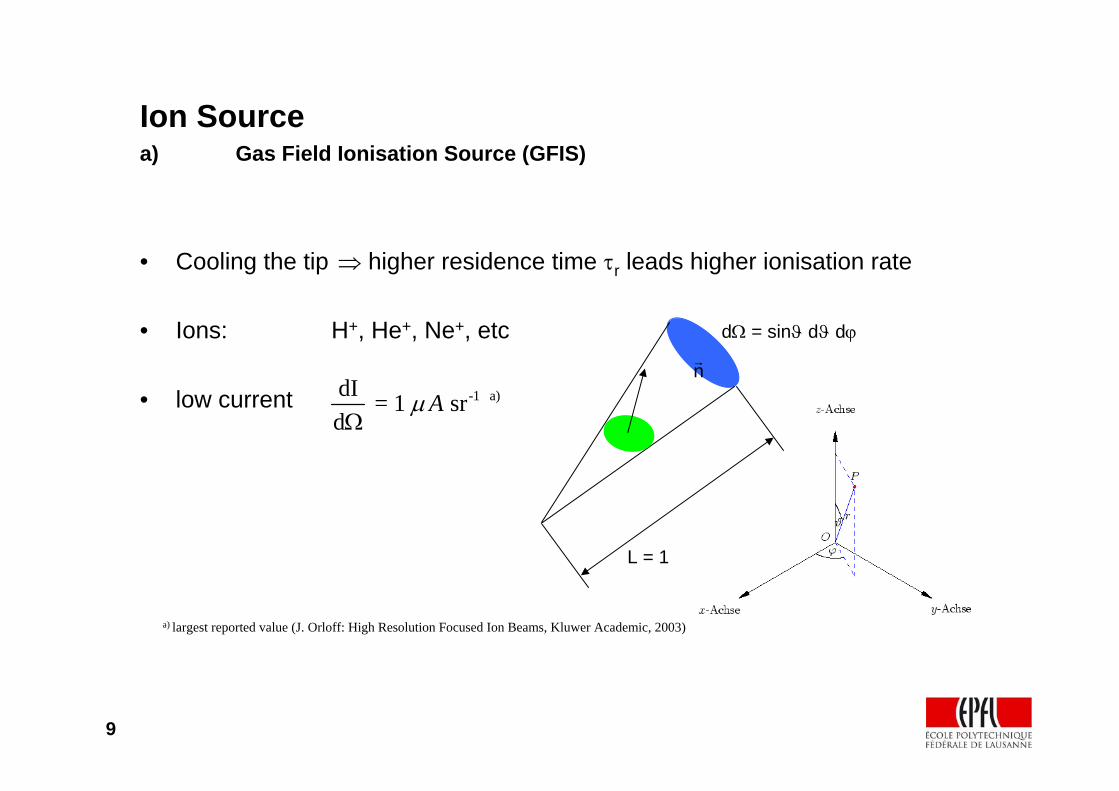
Ion Sourcea) Gas Field Ionisation Source (GFIS)
• Cooling the tip ⇒ higher residence time τr leads higher ionisation rate
• Ions: H+, He+, Ne+, etc
• low current -1 a)dI = 1 sr d
AμΩ
a) largest reported value (J. Orloff: High Resolution Focused Ion Beams, Kluwer Academic, 2003)
dΩ = sinϑ dϑ dϕ
L = 1
n
10
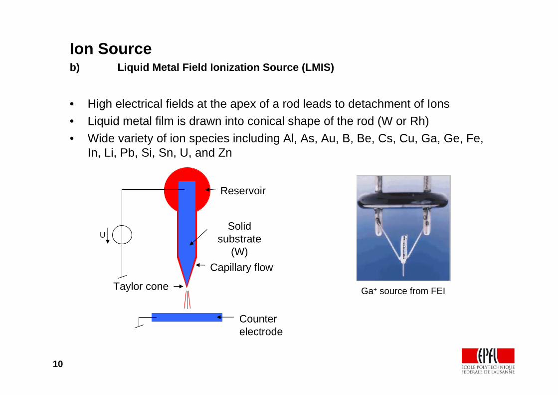
Ion Sourceb) Liquid Metal Field Ionization Source (LMIS)
• High electrical fields at the apex of a rod leads to detachment of Ions• Liquid metal film is drawn into conical shape of the rod (W or Rh)• Wide variety of ion species including Al, As, Au, B, Be, Cs, Cu, Ga, Ge, Fe,
In, Li, Pb, Si, Sn, U, and Zn
Reservoir
Solid substrate
(W)Capillary flow
U
Counter electrode
Ga+ source from FEITaylor cone
11
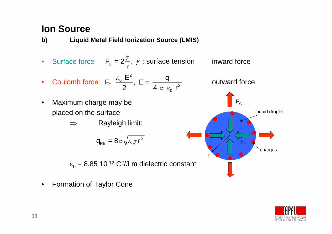
Ion Sourceb) Liquid Metal Field Ionization Source (LMIS)
• Surface force inward force
• Coulomb force outward force
• Maximum charge may beplaced on the surface
⇒ Rayleigh limit:
ε0 = 8.85 10-12 C2/J m dielectric constant
• Formation of Taylor Cone
Liquid droplet
charges
SF = 2 , : surface tensionrγ γ
20
C 20
E qF , E = 2 4 r
επ ε
FS
FC
3Rh 0q = 8 rπ ε γ
r
12
Ion Sourceb) Liquid Metal Field Ionization Source (LMIS)
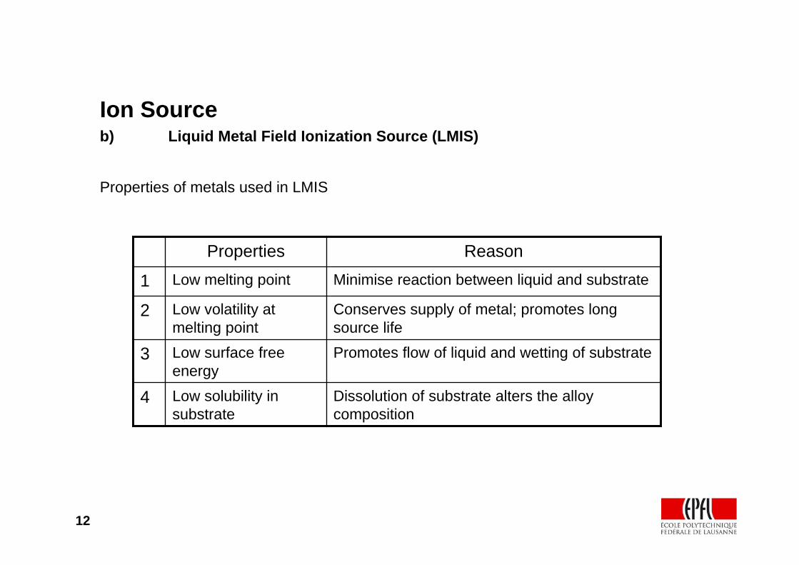
Properties of metals used in LMIS
Promotes flow of liquid and wetting of substrateLow surface free energy
3
Dissolution of substrate alters the alloy composition
Low solubility in substrate
4
Conserves supply of metal; promotes long source life
Low volatility at melting point
2
Minimise reaction between liquid and substrateLow melting point1
ReasonProperties
13
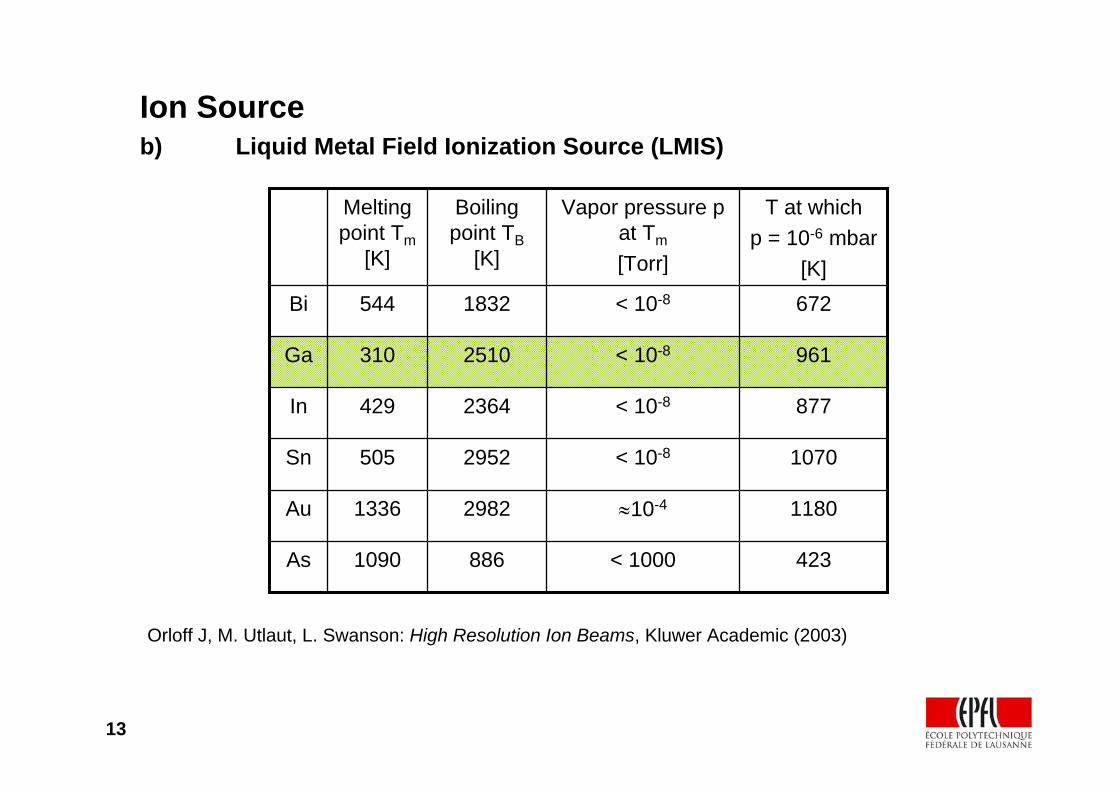
Ion Sourceb) Liquid Metal Field Ionization Source (LMIS)
1180≈10-429821336Au
877< 10-82364429In
1070< 10-82952505Sn
423
961
672
T at whichp = 10-6 mbar
[K]
< 10008861090As
< 10-82510310Ga
< 10-81832544Bi
Vapor pressure p at Tm
[Torr]
Boiling point TB
[K]
Melting point Tm
[K]
Orloff J, M. Utlaut, L. Swanson: High Resolution Ion Beams, Kluwer Academic (2003)
14
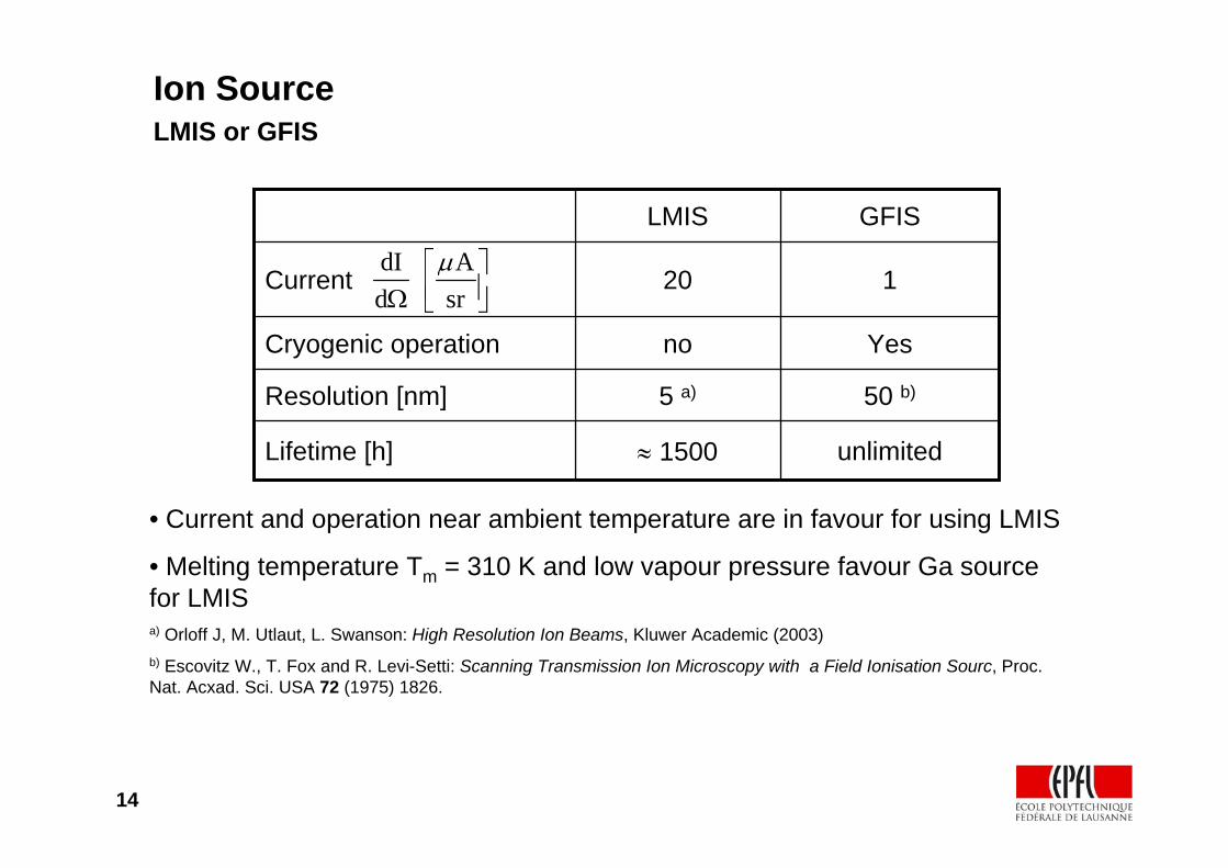
Ion SourceLMIS or GFIS
unlimited≈ 1500Lifetime [h]
50 b)5 a)Resolution [nm]
YesnoCryogenic operation
120Current
GFISLMIS
dI A d sr
μ⎡ ⎤⎢ ⎥Ω ⎣ ⎦
• Current and operation near ambient temperature are in favour for using LMIS
• Melting temperature Tm = 310 K and low vapour pressure favour Ga source for LMISa) Orloff J, M. Utlaut, L. Swanson: High Resolution Ion Beams, Kluwer Academic (2003)b) Escovitz W., T. Fox and R. Levi-Setti: Scanning Transmission Ion Microscopy with a Field Ionisation Sourc, Proc. Nat. Acxad. Sci. USA 72 (1975) 1826.
15
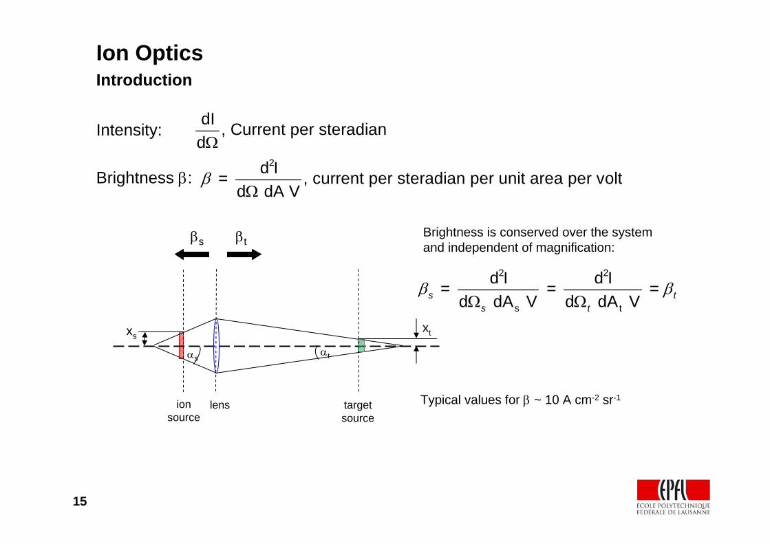
Ion OpticsIntroduction
Intensity:
Brightness β:
dI , Current per steradiandΩ
2d I = , current per steradian per unit area per voltd dA V
βΩ
lension source
target source
xsxt
αsαt
Brightness is conserved over the system and independent of magnification:
2 2
s t
d I d I = = = d dA V d dA Vs t
s t
β βΩ Ω
βs βt
Typical values for β ~ 10 A cm-2 sr-1
16
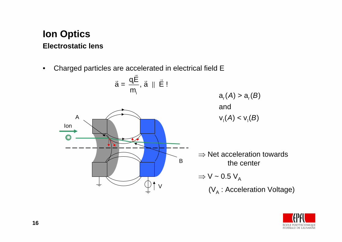
Ion OpticsElectrostatic lens
• Charged particles are accelerated in electrical field E
i
i
qEa = , a E !m
V
A
B⇒ Net acceleration towards
the center
⇒ V ~ 0.5 VA
(VA : Acceleration Voltage)
r r
l l
a ( ) > a ( )andv ( ) < v ( )
A B
A BIon
17
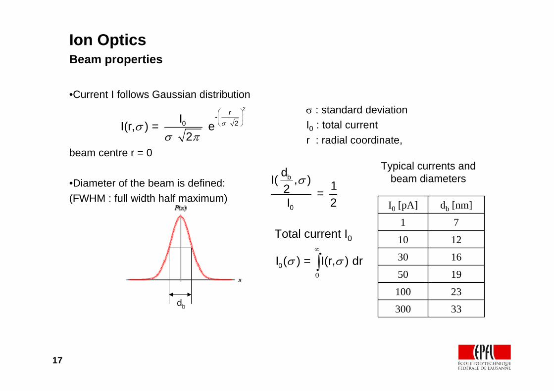
Ion OpticsBeam properties
•Current I follows Gaussian distributionσ : standard deviationI0 : total currentr : radial coordinate,
beam centre r = 0
•Diameter of the beam is defined:(FWHM : full width half maximum)
2
-20II(r, ) = e
2
rσσ
σ π
⎛ ⎞⎜ ⎟⎝ ⎠
db
b
0
dI( , ) 12 = I 2
σ
00
I ( ) = I(r, ) drσ σ∞
∫
Total current I0
33300
23100
1950
1630
1210
71
db [nm]I0 [pA]
Typical currents and beam diameters
18
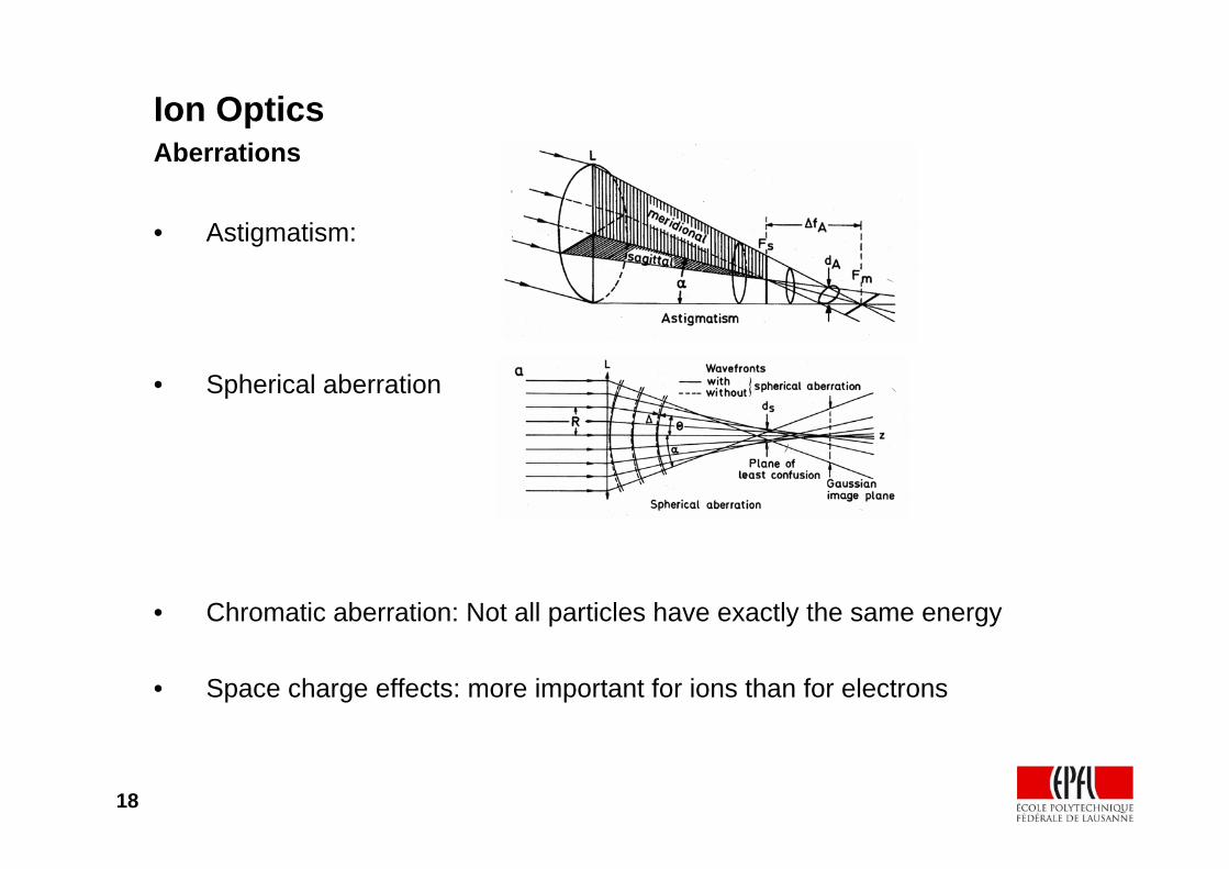
Ion OpticsAberrations
• Astigmatism:
• Spherical aberration
• Chromatic aberration: Not all particles have exactly the same energy
• Space charge effects: more important for ions than for electrons
19
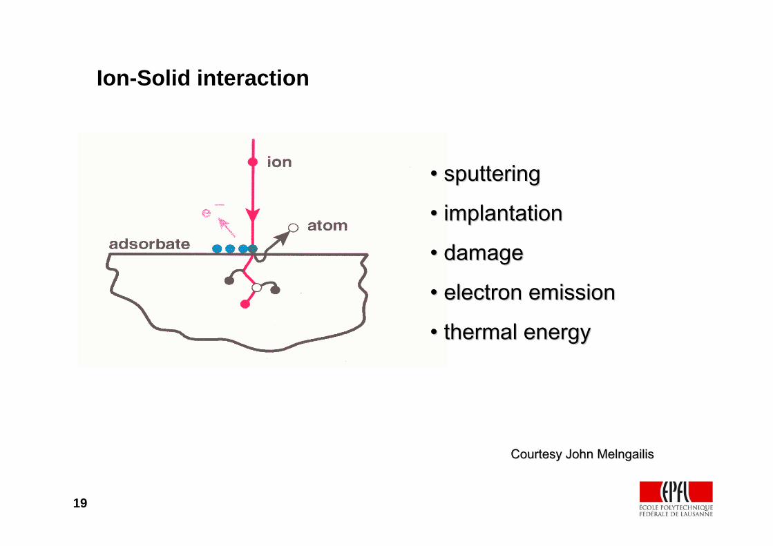
Ion-Solid interaction
•• sputteringsputtering
•• implantationimplantation
•• damage damage
•• electron emissionelectron emission
•• thermal energythermal energy
Courtesy John Courtesy John MelngailisMelngailis
20
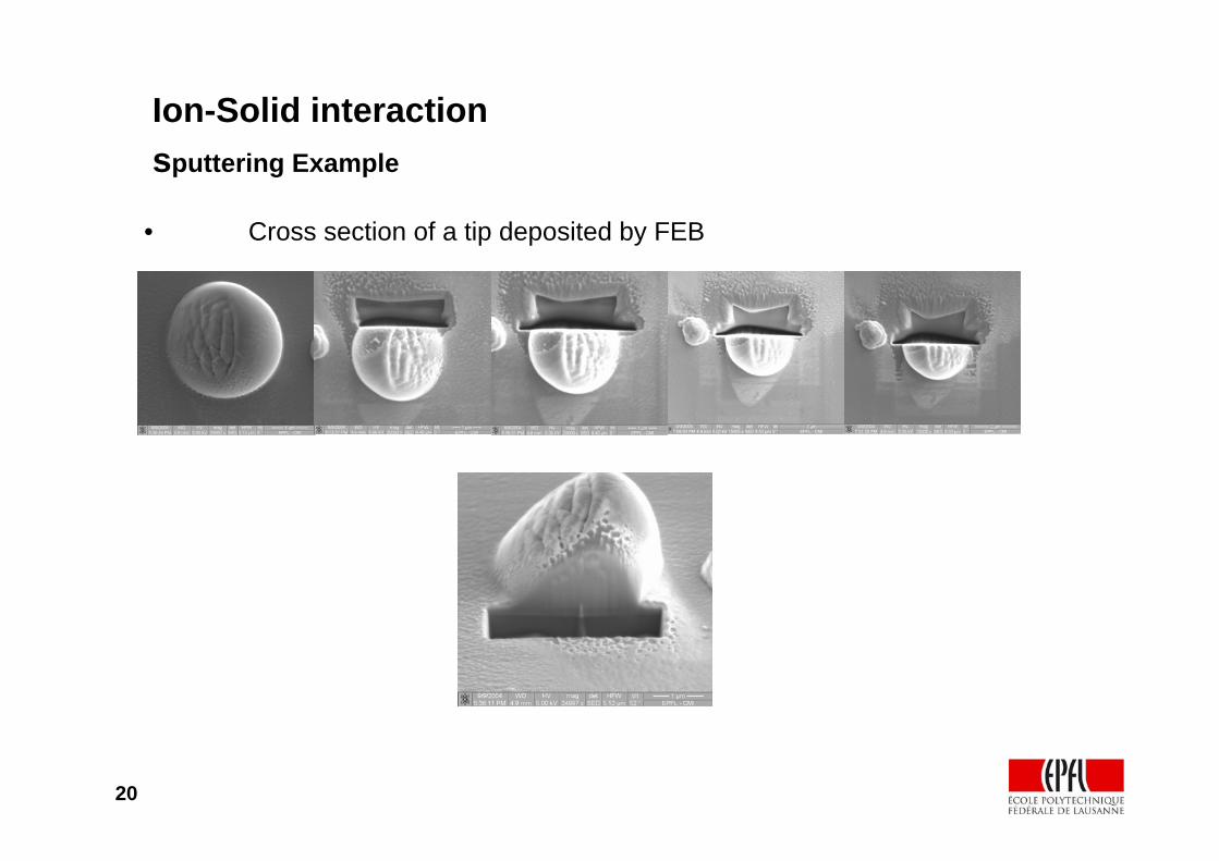
Ion-Solid interactionsputtering Example
• Cross section of a tip deposited by FEB
21
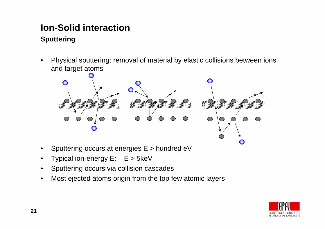
Ion-Solid interactionSputtering
• Physical sputtering: removal of material by elastic collisions between ions and target atoms
• Sputtering occurs at energies E > hundred eV• Typical ion-energy E: E > 5keV• Sputtering occurs via collision cascades• Most ejected atoms origin from the top few atomic layers
22
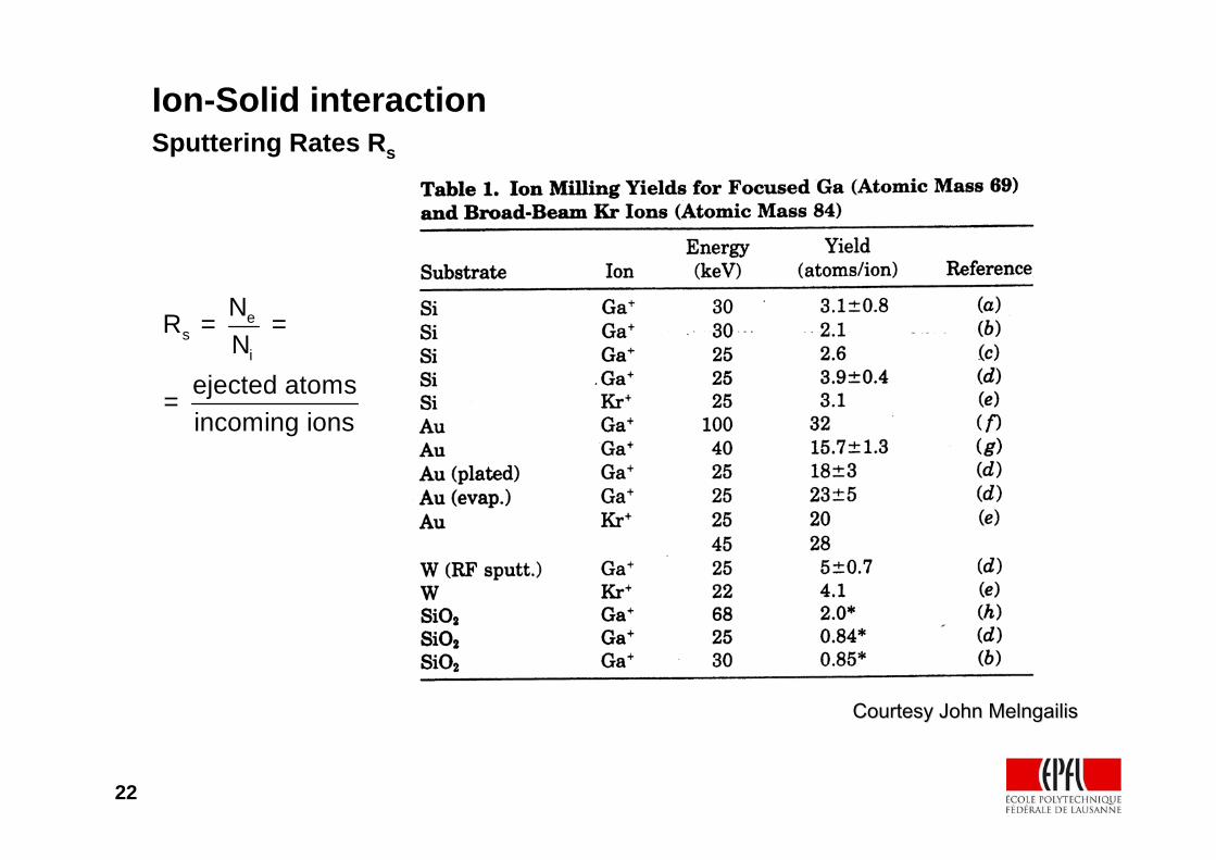
Ion-Solid interactionSputtering Rates Rs
Courtesy John Courtesy John MelngailisMelngailis
es
i
NR = =N
ejected atoms= incoming ions
23
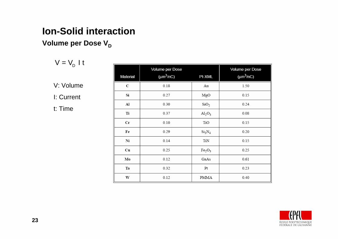
Ion-Solid interactionVolume per Dose VD
DV = V I t
V: Volume
I: Current
t: Time
24
Ion-Solid interactionSputtering Yield
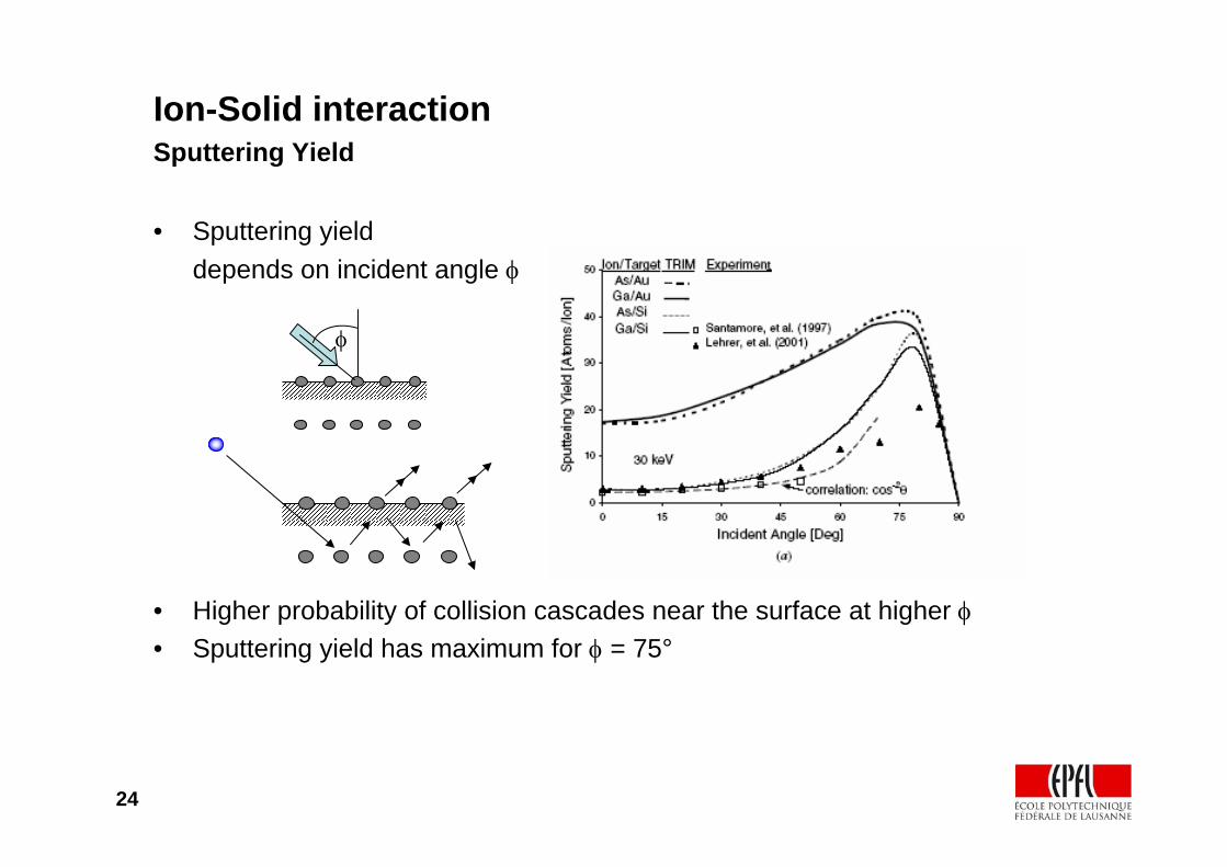
• Sputtering yielddepends on incident angle φ
• Higher probability of collision cascades near the surface at higher φ• Sputtering yield has maximum for φ = 75°
φ
25
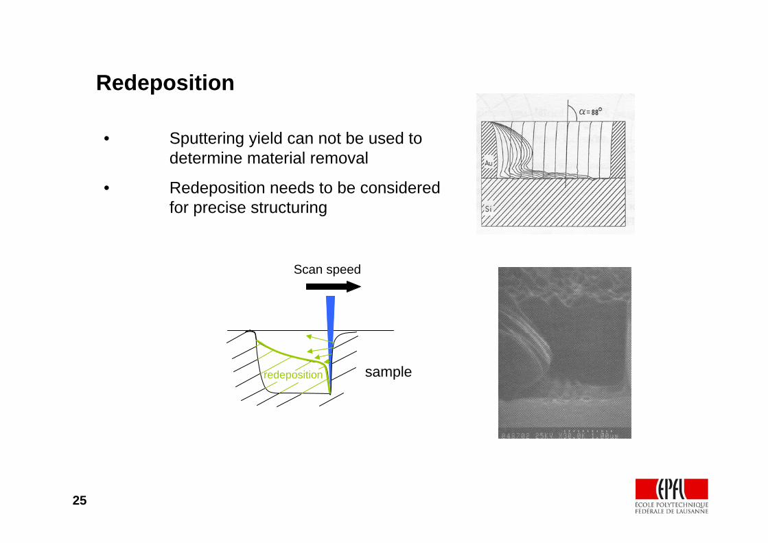
Redeposition
redeposition
Scan speed
sample
• Sputtering yield can not be used to determine material removal
• Redeposition needs to be considered for precise structuring
26
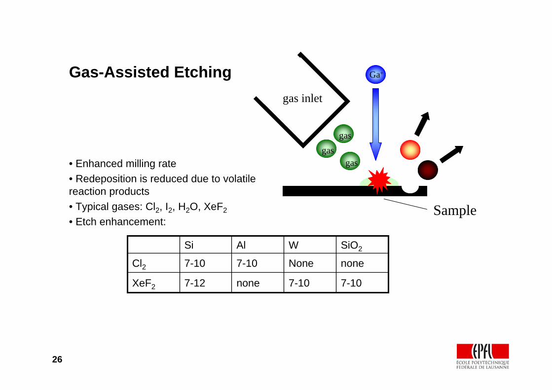
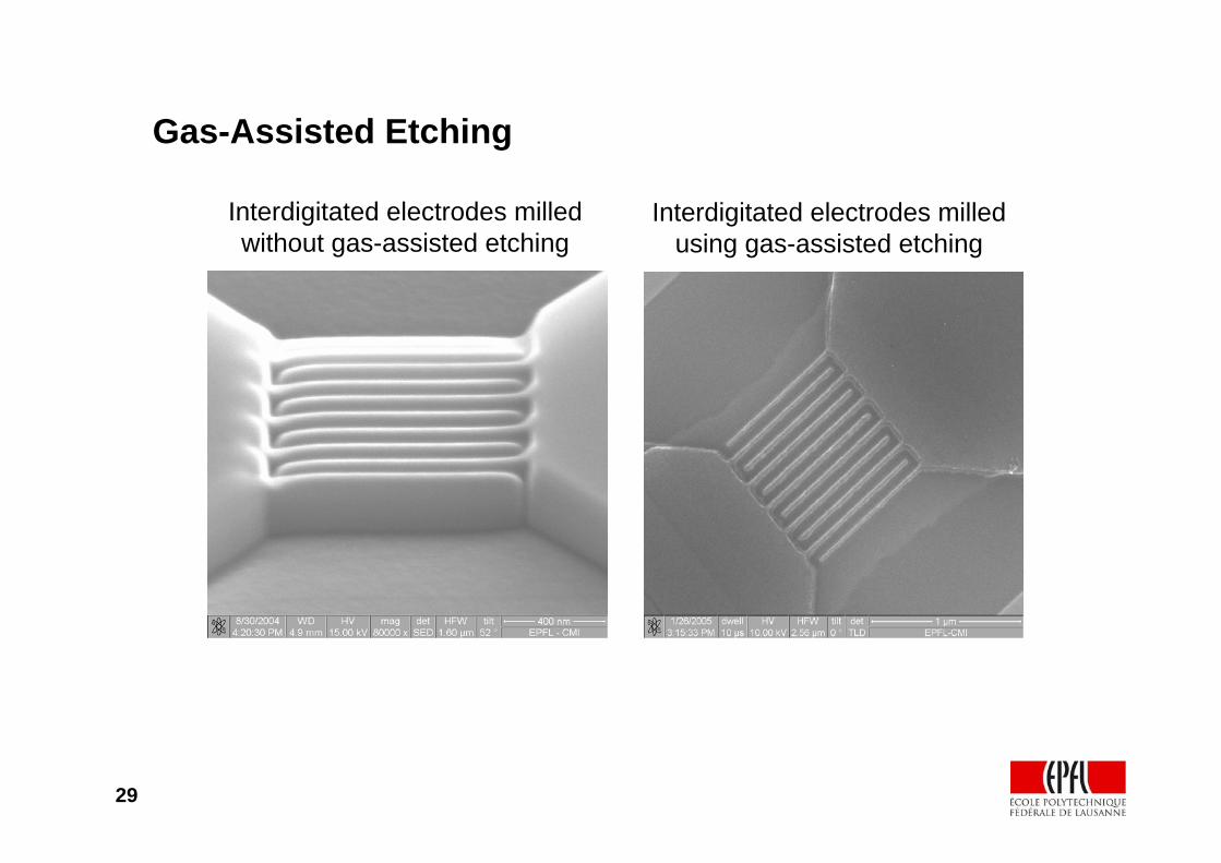
Gas-Assisted Etching
• Enhanced milling rate• Redeposition is reduced due to volatile reaction products• Typical gases: Cl2, I2, H2O, XeF2
• Etch enhancement:Sample
Ga+
gas
gasgas
gas inlet
7-10
None
W
7-10none7-12XeF2
none7-107-10Cl2
SiO2AlSi
27
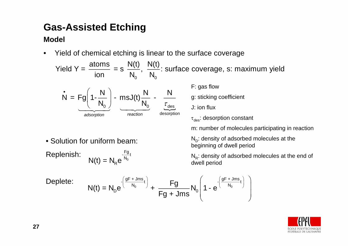
• Yield of chemical etching is linear to the surface coverage
Gas-Assisted EtchingModel
0 0
atoms N(t) N(t)Yield Y = = s , : surface coverage, s: maximum yieldion N N
0 0 desdesorption
N N NN = Fg 1- - msJ(t) - N N
reactionadsorption
τ
• ⎛ ⎞⎜ ⎟⎝ ⎠
F: gas flow
g: sticking coefficient
J: ion flux
τdes: desorption constant
m: number of molecules participating in reaction
ND: density of adsorbed molecules at the beginning of dwell period
NR: density of adsorbed molecules at the end of dwell period
• Solution for uniform beam:
Replenish:
Deplete:0 0
gF + Jms gF + Jms- t - tN N
D 0FgN(t) = N e + N 1 - e
Fg + Jms
⎛ ⎞ ⎛ ⎞⎜ ⎟ ⎜ ⎟⎝ ⎠ ⎝ ⎠
⎛ ⎞⎜ ⎟⎜ ⎟⎝ ⎠
0
Fg- tN
RN(t) = N e
28
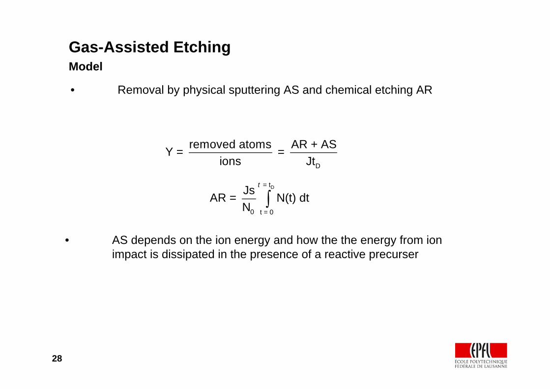
Gas-Assisted EtchingModel
• Removal by physical sputtering AS and chemical etching AR
D
removed atoms AR + ASY = = ions Jt
D = t
0 t = 0
JsAR = N(t) dtN
t
∫
• AS depends on the ion energy and how the the energy from ion impact is dissipated in the presence of a reactive precurser
29
Gas-Assisted Etching
Interdigitated electrodes milled without gas-assisted etching
Interdigitated electrodes milled using gas-assisted etching
30
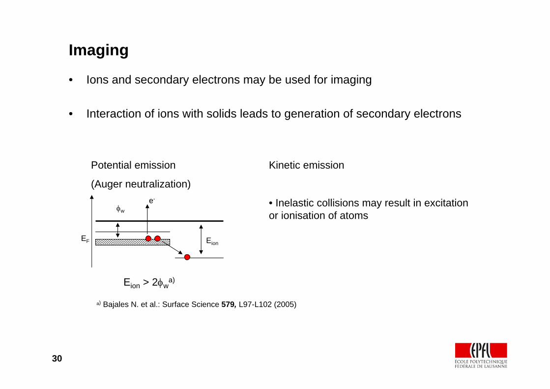
Imaging
• Ions and secondary electrons may be used for imaging
• Interaction of ions with solids leads to generation of secondary electrons
Eion
e-
φw
Potential emission
(Auger neutralization)
EF
Eion > 2φwa)
Kinetic emission
• Inelastic collisions may result in excitation or ionisation of atoms
a) Bajales N. et al.: Surface Science 579, L97-L102 (2005)
31
Imaging
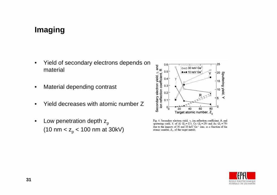
• Yield of secondary electrons depends on material
• Material depending contrast
• Yield decreases with atomic number Z
• Low penetration depth zp
(10 nm < zp < 100 nm at 30kV)
32
ImagingFIB and Electron Microscopy - a Comparison
Resolution:FIB and SEM are comparable; FIBs: up to 5nm, SEMs: up to 3nm
Sample handling:Both FIB and SEM comparable
Voltage contrast imaging:FIB performs better than low-voltage SEM (low intrinsic depth of ions)
Material analysis:SEM allows EDX, FIB doesn't (excication energy !). FIB would allow micro-
SIMS (some systems are installed)
33
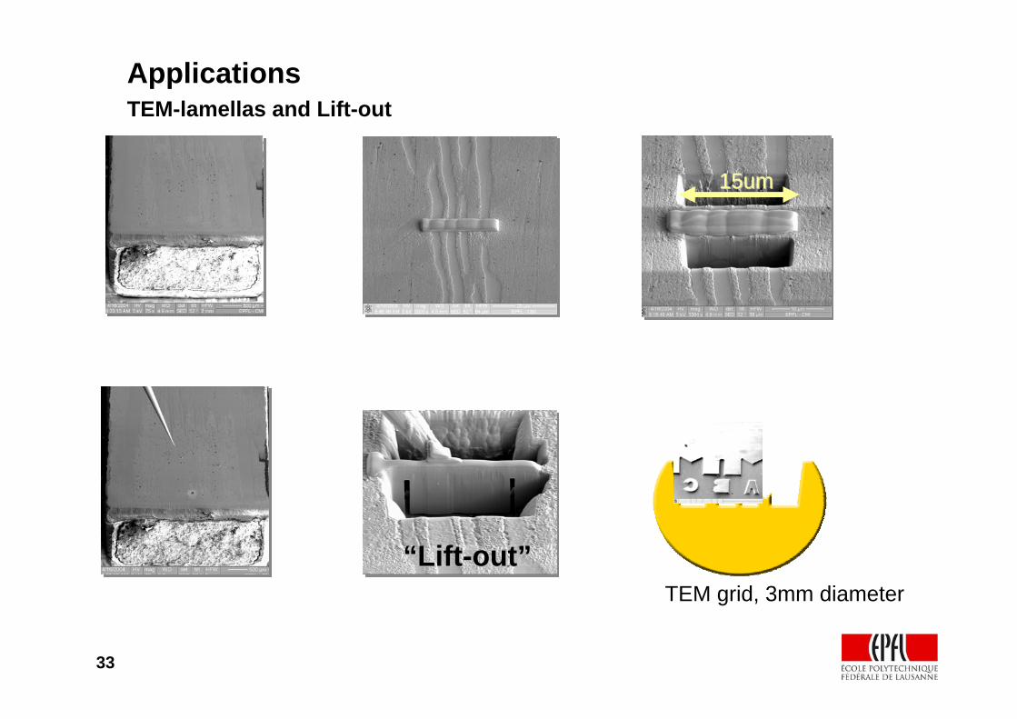
ApplicationsTEM-lamellas and Lift-out
TEM grid, 3mm diameter““LiftLift--outout””
15um15um
34
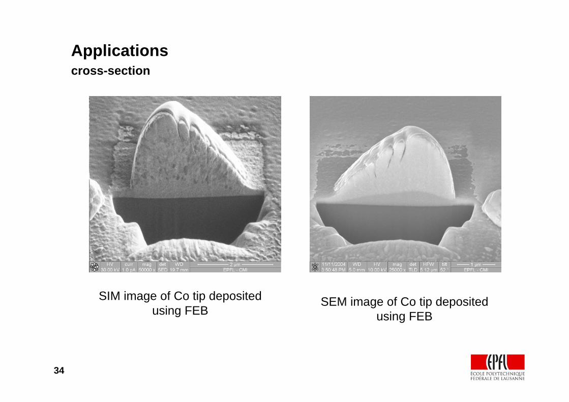
Applicationscross-section
SIM image of Co tip deposited using FEB
SEM image of Co tip deposited using FEB
35
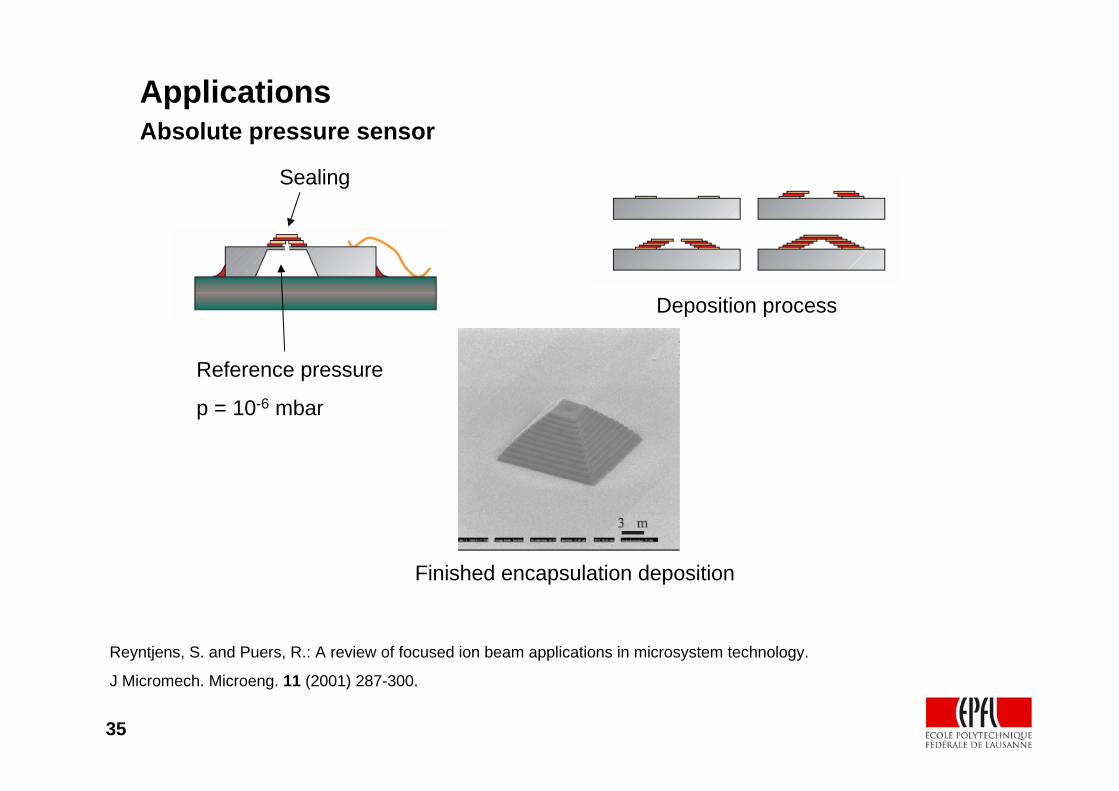
ApplicationsAbsolute pressure sensor
Reference pressure
p = 10-6 mbar
Sealing
Deposition process
Finished encapsulation deposition
Reyntjens, S. and Puers, R.: A review of focused ion beam applications in microsystem technology.
J Micromech. Microeng. 11 (2001) 287-300.
36
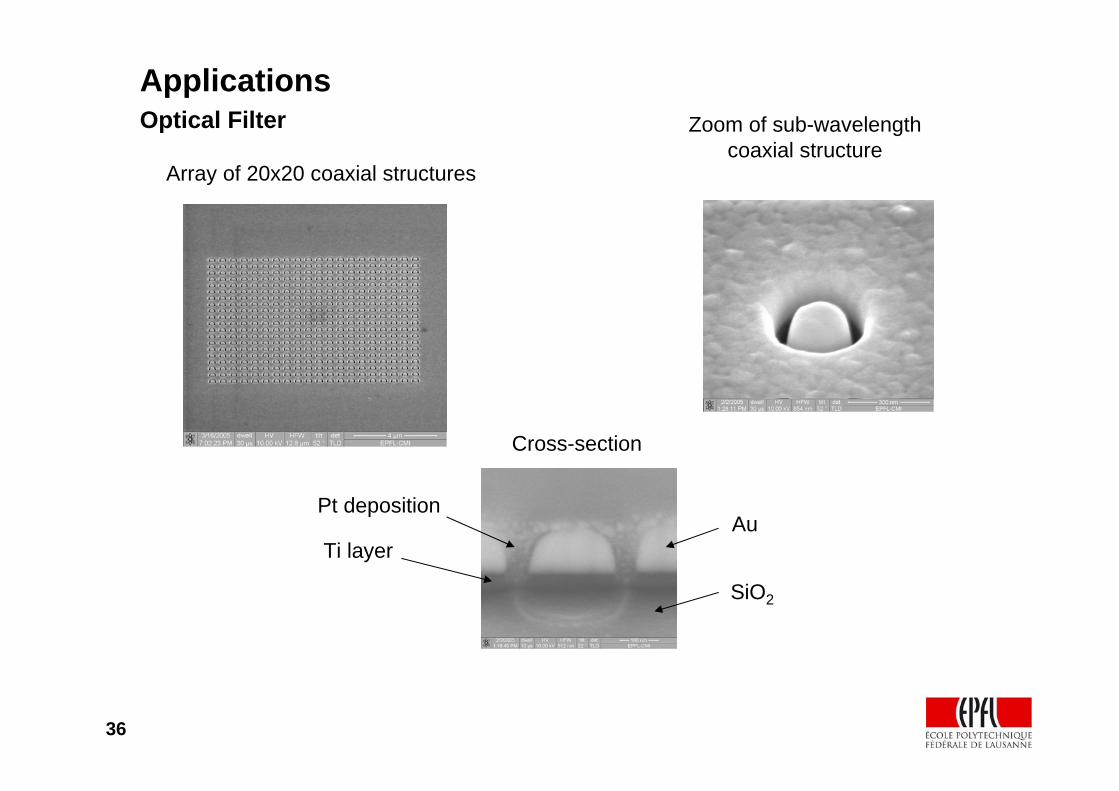
ApplicationsOptical Filter
Au
SiO2
Ti layer
Pt deposition
Cross-section
Zoom of sub-wavelength coaxial structure
Array of 20x20 coaxial structures
37
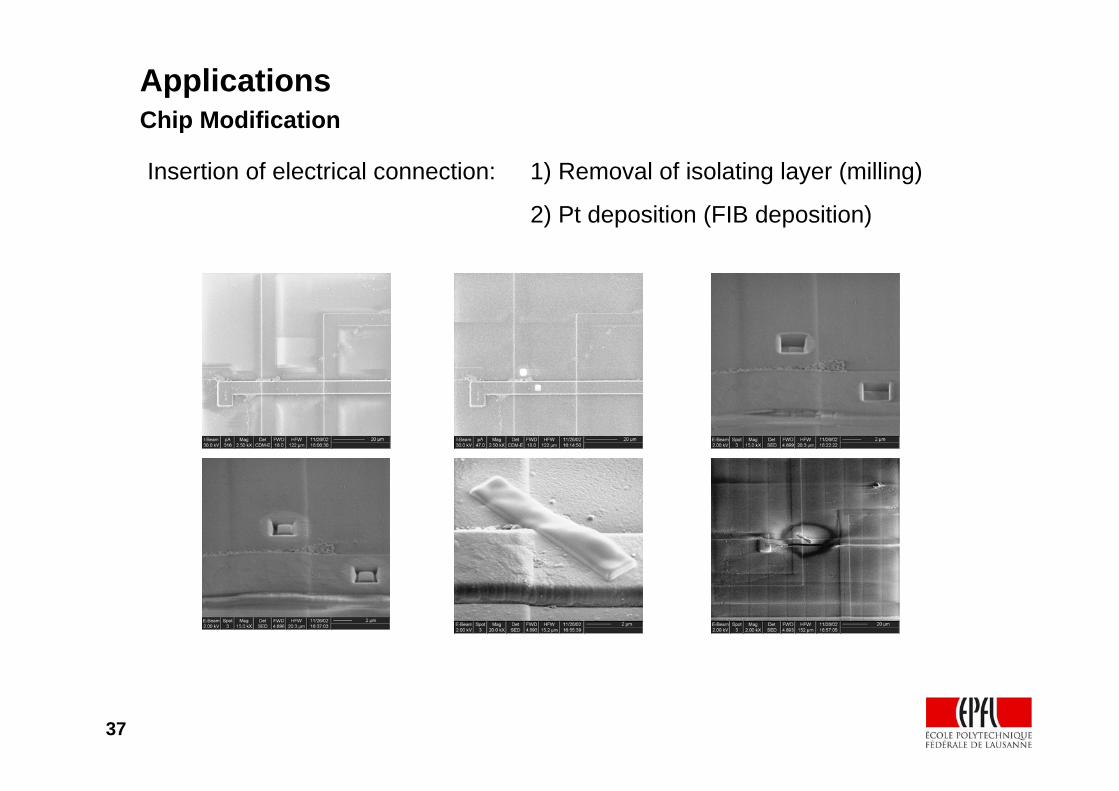
ApplicationsChip Modification
Insertion of electrical connection: 1) Removal of isolating layer (milling)
2) Pt deposition (FIB deposition)