fo-plp benefits for high performance applications in ... · 2 contents i. automotive industry trend...
TRANSCRIPT

1
Semiconductor
Neuromorphic A.I
IT Materials
Functional Film
LED/ENC
FO-PLP Benefits for High Performance
Applications in Automotive
nepes Corporation
Lewis KangOctober 17, 2018

2
Contents
I. Automotive Industry Trend & SiP
II. nepes Packages for Automotive
III. FO-PLP (Fan out-Panel Level Package) Technology
IV. Summary

3
I. Automotive Industry Trend & SiP

4
Driving Applications
Consumer Automotive
• Application Processor/Base Band
• Micro Controller Unit
• Biometric Sensors
• Power Management IC
• RF Devices
• Display Driver IC
• MEMS Sensors
• Radar (Transceiver, Receiver, VCO)
• Micro Controller Unit
• Sensors
• HBM Memory
• Discrete Power Devices
• Analog ICs
Packaging Technology Innovation !!!

5
Automotive Electronics Application Modules
Instrumentation- Instrument Cluster
- Head-Up Display
Powertrain- Engine Control Module
- Transmission Control
Module
Safety- Airbag Control Module
- Airbag Crash Sensors
- Event Data Recorder
ADAS- ADAS Control Module
- Camera Modules
- Sensor Modules
- V2X Communications
Aftermarket- Portable Navi Devices
- Audio Head Units
- Infotainment Head Units
- Video Recorders
Body- Climate Control
- Remote Keyless Entry
- Lighting
- Electronic Control Units
Chassis- Antilock Braking (ABS)
- Stability Control
- Tire Pressure Monitoring
- Steer/Brake-by-Wire
EV/HEV- Electric Drive Controller
- Battery Management
- Inverter
Infotainment - Audio Head Units
- Fixed Navi System
- Infotainment Head Units
- Rear Seat Entertainment
**ADAS : Advanced Driver Assistance System
**EV/HEV : Electric Vehicle & Hybrid
(source : IHS, Gartner)
6
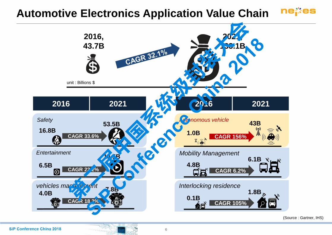
Automotive Electronics Application Value Chain
(Source : Gartner, IHS)
Entertainment
Interlocking residence
Safety
vehicles management
Autonomous vehicle
Mobility Management
16.8B53.5B
1.0B
43B
6.5B
14.5B
4.8B6.1B
4.0B7.8B
0.1B1.8B
CAGR 33.6%
CAGR 22.2%
CAGR 18.2%
CAGR 156%
CAGR 6.2%
CAGR 105%
2016,
43.7B
2021,
133.1B
2016 2021 2016 2021
unit : Billions $

7
System in Package?
▪ FUNCTIONAL SYSTEM or SUBSYSTEM
Assembled into a standard footprint package ; LGA, BGA, QFN or FOWLP
▪ TWO or MORE DISSIMILAR DIE, typically combined with other components;
passives, filters, MEMS, sensors, and/or antennas; forms a FUNCTIONAL BLOCK

8
SiP Driving Force
▪ MOBILE ELECTRONIC PRODUCT (SMARTPHONEs, TABLETs … )
(with ever-increasing functionality in the less SPACE and the demand for
CONNECTIVITY everywhere) >>> MINIATURIZATION.
Performance
Reason for
SiP adoption
Miniaturization
Integration
Mixed process
Sys. Flexibility
Cost reduction
Form factor such as
package height, footprint
Different device types such
as RF, analog, memory
Die fabricated on different
silicon technology nodes
System performance
(signal integrity, power
consumption), Optimization
Simplication of module level
test and qualification
Higher production efficiency
Reduced system BOM and
complexity, simplified product
board and faster time to market
Source :Techsearch

9
II. nepes Packages for Automotive

10
nepes Technologies in Automotive
▪ Key products – Cu pillar bump
Stacked RDL(Cu/Ni/Au) for power device
FOWLP for sensor package in safety system
Powertrain- Engine Motor IC - QFP PKG /CNA RDL, Cu
pillar
Safety- Airbag - QFN PKG /CNA RDL
ADAS system - RADAR Sensor - FO-WLP
Chassis- Brake system- QFN PKG /CNA RDL , Cu
pillar
Infotainment - Audio Drive IC - QFP /CNA RDL

11
Fan Out WLP, Applications
➢ Small (6x6mm, 1 metal layer), Short transmission lines
➢ Can expose back of die for heatsink
➢ Embedded Ground Plane for ground and shielding
➢ Can embed an antenna structure
▪ 77 GHz Radar
▪ Excellent RF isolation, controlled impedance, low insertion loss, low
attenuation, good thermal dissipation and automotive reliability

12
Fan Out WLP, Applications
▪ 77 GHz Radar

13
3D Fan Out WLP : Double side
[FOWLP : PoP w/ Double Side RDL
2-RDLs
Line&Space 10/10um
[ Reliability ]
Solder BallBuild-up
(PI 1~3 / RDL 1~2)
▪ FOWLP (SiP) supporting PoP of commercial package (upper)
▪ Vertical Interconnection without TMV technology
▪ Thin Profile: 0.35T w/o Solder Ball
▪ RDL Line & Space: 10um/10um

14
Pressure Sensor
< 3D FOP Structure >< Existing Solutions>Small/Thin
Integration
Low cost
Side by side
Die stacking
▪ Integration of MEMS and ASIC controller
▪ LGA pad on package bottom & Fan-Out PoP bottom package with wire
bondable pad on top-side
▪ Smaller/Thinner Form-factor (2x2mm2, 0.2mm thin) with Via- frame vertical
interconnection

15
Computer within a hand!!
▪ Applications
- Digital signage, Human-machine interface
- Home energy management systems
- In-flight entertainment
- Intelligent industrial control systems
- IP phones, IPTV, Portable medical, Smart books
- Point-of-sale devices, Smart watches
- Home audio systems, Secure smart connected devices
PoP Module Package
• Package size : 17 x 14 x 1.7 mm3
• IC: AP, PMIC, Flash Memory
• Over 100 discrete components
3D System Package

16
▪ Big data era drives optical interconnect replacing traditional metal
interconnect even at short distance
▪ Concerns are ;
- Signal loss at wire bonding
- Complicate assembly – fiber alignment & assembly
- Form factor
Optical Communication Module
Optical
IC
CFPCFP
2
QSF
P
CFP
4 CX
P
Tx Rx

17
Optical Communication Module
< Transmitter > < Receiver ><E-Board>
➢ ≥ 6Gbps / channel (upto 8Gbps /channel)
➢Raise & fall time = ~ 110ps
▪ Package level OSA based on Fan-out process
▪ Electrical Performance

18
III. FO-PLP (Fan out-Panel Level Package)
Technology

19
• Innovative process & structure
• Advanced packaging platform with cost-
effectiveness
FO-PLP (Panel Level Package)
in large Panel @nepes
FO-WLP
@300mm round
PLP (Panel Level Package)

20
Panel Level Package : Solution
FO-PLP
600 x 600mm
Since 2016
FO-WLP since 2009 LCD Panel since 2011
650 x 750mm
Touch Screen Panel300mm
FO-WLP
“Collaboration
& Synergy”
• 4th Gen. Process infrastructure
- 650x750mm
• LCD process know-how
- Panel Handling, Vacuum control, etc.
• Proven film process technology
- Dry film PR, Thin-film tech.
• Core technology know-how
- Die drift or Warpage Control
• Wafer-level experience since 2001
- 150mm, 200mm, 300mm
- Process know-how (Bumping, RDL)
• Fan-Out Package R&D records
- SiP, 4 metal layers, 2 sides RDLs
▪ Hybrid Process Technology between FOWLP & LCD
▪ Advanced packaging platform with cost competitiveness

21
Panel Level Package : Application
⚫ ADAS Radar Sensor• RF Performance (77GHz)
• Thermal Dissipation
• High Reliability
⚫ RF, Power, Audio, etc.• Performance, Form factor
⚫ Antenna Switch• Multi-chip Integration
⚫ Bluetooth Low Energy
Si Compund
EMC
⚫ System in Package• Multi-Die, Passives, 4 RDL Layers
EMC
⚫ FPS, Bio & Medical Sensor• Face-up, Via-frame, Open Cavity
⚫ Photonics• Low cost & Easy Optical Alignment
ChipChipEMC
EGP
ChipChip
EMC

22
IV. Summary

23
Summary

24
“Co-development for
competitive edge of
customer”
• Fingerprint Sensor
• Automotive Radar
“Co-investment for packaging
technology innovation”• Stock share, JV
• PLP consortium
“Co-challenge to nurture
the packaging industry”• Dielectric material
co-development

25
To Him who alone does great wonders, His love endures forever. Psalm 136:4
* A dandelion means ‘Gratitude’ in the language of flowers.
nepes corporation
2415, Nambusunhwan-ro, Seocho-gu, Seoul, Korea
Tel : 02-3470-2700
Fax : 02-3470-2708
URL: www.nepes.co.kr
Thank you