fm jwbs029-hueber september 2, 2010 10:23...
TRANSCRIPT


fm JWBS029-Hueber September 2, 2010 10:23 Printer: Yet to come
ii
fm JWBS029-Hueber September 2, 2010 10:23 Printer: Yet to come
MULTI-MODE/MULTI-BANDRF TRANSCEIVERS FORWIRELESS COMMUNICATIONS
i

fm JWBS029-Hueber September 2, 2010 10:23 Printer: Yet to come
ii

fm JWBS029-Hueber September 2, 2010 10:23 Printer: Yet to come
MULTI-MODE/MULTI-BANDRF TRANSCEIVERS FORWIRELESS COMMUNICATIONS
Advanced Techniques, Architectures,and Trends
Edited by
Gernot HueberRobert Bogdan Staszewski
A JOHN WILEY & SONS, INC., PUBLICATION
iii
fm JWBS029-Hueber September 2, 2010 10:23 Printer: Yet to come
Copyright C© 2011 by John Wiley & Sons, Inc. All rights reserved.
Published by John Wiley & Sons, Inc., Hoboken, New Jersey.Published simultaneously in Canada.
No part of this publication may be reproduced, stored in a retrieval system, or transmitted in any form orby any means, electronic, mechanical, photocopying, recording, scanning or otherwise, except aspermitted under Sections 107 or 108 of the 1976 United States Copyright Act, without either the priorwritten permission of the Publisher, or authorization through payment of the appropriate per-copy fee tothe Copyright Clearance Center, Inc., 222 Rosewood Drive, Danvers, MA 01923, (978) 750-8400,fax (978) 750-4470, or on the web at www.copyright.com. Requests to the Publisher for permissionshould be addressed to the Permissions Department, John Wiley & Sons, Inc., 111 River Street, Hoboken,NJ 07030, (201) 748-6011, fax (201) 748-6008, or online at http://www.wiley.com/go/permission.
Limit of Liability/Disclaimer of Warranty: While the publisher and author have used their best efforts inpreparing this book, they make no representations or warranties with respect to the accuracy orcompleteness of the contents of this book and specifically disclaim any implied warranties ofmerchantability or fitness for a particular purpose. No warranty may be created or extended by salesrepresentatives or written sales materials. The advice and strategies contained herein may not be suitablefor your situation. You should consult with a professional where appropriate. Neither the publisher norauthor shall be liable for any loss of profit or any other commercial damages, including but not limited tospecial, incidental, consequential, or other damages.
For general information on our other products and services or for technical support, please contact ourCustomer Care Department within the United States at (800) 762-2974, outside the United States at(317) 572-3993 or fax (317) 572-4002.
Wiley also publishes its books in a variety of electronic formats. Some content that appears in print maynot be available in electronic formats. For more information about Wiley products, visit our web site atwww.wiley.com.
Library of Congress Cataloging-in-Publication Data:
Multi-mode/multi-band RF transceivers for wireless communications : advanced techniques,architectures, and trends / edited by Gernot Hueber and Robert Bogdan Staszewski.
p. cm.Includes bibliographical references and index.ISBN 978-0-470-27711-91. Radio–Transmitter-receivers. 2. Wireless communication systems–Equipment and
supplies–Design and construction. 3. Cellular telephones–Design and construction.4. Wireless LANs–Equipment and supplies–Design and construction. I. Hueber, Gernot, 1972–II. Staszewski, Robert Bogdan, 1965–
TK6564.3.M85 2011384.5′3–dc22
2010001881
Printed in Singapore
10 9 8 7 6 5 4 3 2 1
iv

fm JWBS029-Hueber September 2, 2010 10:23 Printer: Yet to come
CONTENTS
Contributors xi
Preface xiii
I TRANSCEIVER CONCEPTS AND DESIGN 1
1 Software-Defined Radio Front Ends 3Jan Craninckx
1.1 Introduction 31.2 System-Level Considerations 41.3 Wideband LO Synthesis 51.4 Receiver Building Blocks 121.5 Transmitter Building Blocks 231.6 Calibration Techniques 251.7 Full SDR Implementation 271.8 Conclusions 30
References 30
2 Software-Defined Transceivers 33Gio Cafaro and Bob Stengel
2.1 Introduction 332.2 Radio Architectures 342.3 SDR Building Blocks 342.4 Example of an SDR Transceiver 54
References 60
3 Adaptive Multi-Mode RF Front-End Circuits 65Aleksandar Tasic
3.1 Introduction 653.2 Adaptive Multi-Mode Low-Power Wireless RF
IC Design 663.3 Multi-Mode Receiver Concept 683.4 Design of a Multi-Mode Adaptive RF Front End 70
v

fm JWBS029-Hueber September 2, 2010 10:23 Printer: Yet to come
vi CONTENTS
3.5 Experimental Results for the Image-RejectDown-Converter 76
3.6 Conclusions 80References 81
4 Precise Delay Alignment Between Amplitude and Phase/Frequency Modulation Paths in a Digital Polar Transmitter 85Khurram Waheed and Robert Bogdan Staszewski
4.1 Introduction 854.2 RF Polar Transmitter in Nanoscale CMOS 874.3 Amplitude and Phase Modulation 904.4 Mechanisms to Achieve Subnanosecond Amplitude and
Phase Modulation Path Alignments 964.5 Precise Alignment of Multi-Rate Direct and Reference
Point Data 101References 109
5 Overview of Front-End RF Passive Integration into SoCs 113Hooman Darabi
5.1 Introduction 1135.2 The Concept of a Receiver Translational Loop 1195.3 Feedforward Loop Nonideal Effects 1225.4 Feedforward Receiver Circuit Implementations 1255.5 Feedforward Receiver Experimental Results 1295.6 Feedback Notch Filtering for a WCDMA Transmitter 1335.7 Feedback-Based Transmitter Stability Analysis 1385.8 Impacts of Nonidealities in Feedback-Based
Transmission 1415.9 Transmitter Building Blocks 148
5.10 Feedback-Based Transmitter Measurement Results 1505.11 Conclusions and Discussion 153
Appendix 155References 156
6 ADCs and DACs for Software-Defined Radio 159Michiel Steyaert, Pieter Palmers, and Koen Cornelissens
6.1 Introduction 1596.2 ADC and DAC Requirements in Wireless Systems 1606.3 Multi-Standard Transceiver Architectures 1626.4 Evaluating Reconfigurability 1656.5 ADCs for Software-Defined Radio 1666.6 DACs for Software-Defined Radio 1726.7 Conclusions 184
References 184

fm JWBS029-Hueber September 2, 2010 10:23 Printer: Yet to come
CONTENTS vii
II RECEIVER DESIGN 187
7 OFDM Transform-Domain Receivers for Multi-StandardCommunications 189Sebastian Hoyos
7.1 Introduction 1897.2 Transform-Domain Receiver Background 1907.3 Transform-Domain Sampling Receiver 1917.4 Digital Baseband Design for the TD Receiver 1957.5 A Comparative Study 2047.6 Simulations 2087.7 Gain–Bandwidth Product Requirement for an Op-Amp in a
Charge-Sampling Circuit 2117.8 Sparsity of (G H G)−1 2137.9 Applications 214
7.10 Conclusions 215References 216
8 Discrete-Time Processing of RF Signals 219Renaldi Winoto and Borivoje Nikolic
8.1 Introduction 2198.2 Scaling of an MOS Switch 2218.3 Sampling Mixer 2238.4 Filter Synthesis 2268.5 Noise in Switched-Capacitor Filters 2348.6 Circuit-Design Considerations 2378.7 Perspective and Outlook 242
References 244
9 Oversampled ADC Using VCO-Based Quantizers 247Matthew Z. Straayer and Michael H. Perrott
9.1 Introduction 2479.2 VCO-Quantizer Background 2489.3 SNDR Limitations for VCO-Based Quantization 2529.4 VCO Quantizer �� ADC Architecture 2579.5 Prototype �� ADC Example with a VCO Quantizer 2659.6 Conclusions 275
References 276
10 Reduced External Hardware and Reconfigurable RF ReceiverFront Ends for Wireless Mobile Terminals 279Naveen K. Yanduru
10.1 Introduction 27910.2 Mobile Terminal Challenges 280

fm JWBS029-Hueber September 2, 2010 10:23 Printer: Yet to come
viii CONTENTS
10.3 Research Directions Toward a Multi-Band Receiver 28210.4 Multi-Mode Receiver Principles and RF System Analysis for
a W-CDMA Receiver 28610.5 W-CDMA, GSM/GPRS/EDGE Receiver Front End Without
an Interstage SAW Filter 29210.6 Highly Integrated GPS Front End for Cellular Applications in
90-nm CMOS 29910.7 RX Front-End Performance Comparison 305
References 305
11 Digitally Enhanced Alternate Path Linearizationof RF Receivers 309Edward A. Keehr and Ali Hajimiri
11.1 Introduction 30911.2 Adaptive Feedforward Error Cancellation 31111.3 Architectural Concepts 31311.4 Alternate Feedforward Path Block Design
Considerations 32011.5 Experimental Design of an Adaptively Linearized UMTS
Receiver 33111.6 Experimental Results of an Adaptively Linearized UMTS
Receiver 33611.7 Conclusions 341
References 343
III TRANSMITTER TECHNIQUES 347
12 Linearity and Efficiency Strategies for Next-GenerationWireless Communications 349Lawrence Larson, Peter Asbeck, and Donald Kimball
12.1 Introduction 34912.2 Power Amplifier Function 34912.3 Power Amplifier Efficiency Enhancement 35412.4 Techniques for Linearity Enhancement 36212.5 Conclusions 371
References 372
13 CMOS RF Power Amplifiers for Mobile Communications 377Patrick Reynaert
13.1 Introduction 37713.2 Challenges 37813.3 Low Supply Voltage 378

fm JWBS029-Hueber September 2, 2010 10:23 Printer: Yet to come
CONTENTS ix
13.4 Average Efficiency, Dynamic Range, and Linearity 38113.5 Polar Modulation 38613.6 Distortion in a Polar-Modulated Power Amplifier 39013.7 Design and Implementation of a Polar-Modulated Power
Amplifier 39713.8 Conclusions 408
References 408
14 Digitally Assisted RF Architectures: Two Illustrative Designs 411Joel L. Dawson
14.1 Introduction 41114.2 Cartesian Feedback: The Analog Problem 41214.3 Digital Assistance for Cartesian Feedback 41614.4 Multipliers, Squarers, Mixers, and VGAs: The Analog
Problem 42714.5 Digital Assistance for Analog Multipliers 42914.6 Summary 435
Appendix: Stability Analysis for CartesianFeedback Systems 436References 447
IV DIGITAL SIGNAL PROCESSING FOR RF TRANSCEIVERS 451
15 RF Impairment Compensation for Future Radio Systems 453Mikko Valkama
15.1 Introduction and Motivation 45315.2 Typical RF Impairments 45415.3 Impairment Mitigation Principles 46915.4 Case Studies in I/Q Imbalance Compensation 48015.5 Conclusions 487
References 488
16 Techniques for the Analysis of Digital Bang-Bang PLLs 497Nicola Da Dalt
16.1 Introduction 49716.2 Digital Bang-Bang PLL Architecture 49816.3 Analysis of the Nonlinear Dynamics of the BBPLL 49916.4 Analysis of the BBPLL with Markov Chains 50316.5 Linearization of the BBPLL 50816.6 Comparison of Measurements and Models 526
References 531

fm JWBS029-Hueber September 2, 2010 10:23 Printer: Yet to come
x CONTENTS
17 Low-Power Spectrum Processors for Cognitive Radios 533Joy Laskar and Kyutae Lim
17.1 Introduction 53317.2 Paradigm Shift from SDR to CR 53417.3 Challenge and Trends in RFIC/System 53517.4 Analog Signal Processing 53617.5 Spectrum Sensing 53717.6 Multi-Resolution Spectrum Sensing 53817.7 MRSS Performance 54217.8 Conclusions 555
References 556
Index 557

fm JWBS029-Hueber September 2, 2010 10:23 Printer: Yet to come
CONTRIBUTORS
Peter Asbeck, University of California at San Diego, La Jolla, California
Gio Cafaro, Motorola Labs, Plantation, Florida
Koen Cornelissens, Katholieke Universiteit Leuven, Leuven, Belgium
Jan Craninckx, IMEC, Leuven, Belgium
Nicola Da Dalt, Infineon Technologies, Villach, Austria
Hooman Darabi, Broadcom Corporation, Irvine, California
Joel L. Dawson, Massachusetts Institute of Technology, Cambridge,Massachusetts
Ali Hajimiri, California Institute of Technology, Pasadena, California
Sebastian Hoyos, Texas A&M University, College Station, Texas
Edward A. Keehr, California Institute of Technology, Pasadena, California
Donald Kimball, University of California at San Diego, La Jolla, California
Lawrence Larson, University of California at San Diego, La Jolla, California
Joy Laskar, Georgia Tech, Atlanta, Georgia
Kyutae Lim, Georgia Tech, Atlanta, Georgia
Borivoje Nikolic, University of California, Berkeley, California
Pieter Palmers, Katholieke Universiteit Leuven, Leuven, Belgium
Michael H. Perrott, Massachusetts Institute of Technology, Cambridge,Massachusetts
Patrick Reynaert, Katholieke Universiteit Leuven, Leuven, Belgium
Robert Bogdan Staszewski, Texas Instruments, Dallas, Texas; currently at DelftUniversity of Technology, Delft, The Netherlands
Bob Stengel, Motorola Labs, Plantation, Florida
Michiel Steyaert, Katholieke Universiteit Leuven, Leuven, Belgium
Matthew Z. Straayer, Massachusetts Institute of Technology, Cambridge,Massachusetts
xi

fm JWBS029-Hueber September 2, 2010 10:23 Printer: Yet to come
xii CONTRIBUTORS
Alexander Tasic, Qualcomm, San Diego, California
Mikko Valkama, Tampere University of Technology, Tampere, Finland
Khurram Waheed, Texas Instruments, Dallas, Texas; currently at BitWave Semi-conductors, Lowell, Massachusetts
Renaldi Winoto, University of California, Berkeley, California
Naveen K. Yanduru, Texas Instruments, Dallas, Texas; currently at University ofTexas at Dallas, Richardson, Texas

fm JWBS029-Hueber September 2, 2010 10:23 Printer: Yet to come
PREFACE
Current and future mobile terminals become increasingly complex because they haveto deal with a variety of frequency bands and communication standards. Achievingmulti-band/multi-mode functionality is especially challenging for the radio frequency(RF)-transceiver section, due to limitations in terms of frequency-agile RF compo-nents that meet the demanding cellular performance criteria at costs that are attractivefor mass-market applications. The focus of this volume is on novel transceiver con-cepts for multi-mode/multi-band cellular systems from the antenna to baseband.One approach is based on the integration of digital signal processing capabilitiesimplemented locally on the RF integrated circuit. The utilization of digital signalprocessing capabilities is in line with the ongoing trend toward minimum-feature-sized RF-CMOS in the cellular market, which makes it extremely attractive in termsof flexibility, power consumption, and costs. Moreover, advances in the field of an-tennas, RF-front-end modules and novel analog signal processing architectures arecovered to give a consolidated outlook on future concepts for cellular radios.
This volume summarizes cutting-edge physical-layer technologies for multi-modewireless RF transceivers, specifically RF, analog, and digital circuits and architec-tures, anticipating the major trends and needs of the future wireless system devel-opments. Firsthand materials from distinguished researchers and professionals fromboth academia and industry are collected. Furthermore, this volume offers a compre-hensive treatment of the topic, presenting state-of-the-art technologies and insightcovering all the essential transceiver building blocks to be used in future multi-mode(third generation and beyond) wireless communication systems.
G. HueberR. B. Staszewski
xiii

fm JWBS029-Hueber September 2, 2010 10:23 Printer: Yet to come
xiv
c01 JWBS029-Hueber September 2, 2010 10:26 Printer: Yet to come
PART ITransceiver Concepts and Design
1

c01 JWBS029-Hueber September 2, 2010 10:26 Printer: Yet to come
2

c01 JWBS029-Hueber September 2, 2010 10:26 Printer: Yet to come
1 Software-Defined RadioFront Ends
JAN CRANINCKXIMEC, Leuven, Belgium
1.1 INTRODUCTION
The ultimate dream of every software-defined radio (SDR) front-end architect isto deliver a radio-frequency (RF) transceiver that can be reconfigured into everyimaginable operating mode, in order to comply with the requirements of all existingand even upcoming communication standards. These include a large range of modesfor cellular (2G–2.5G–3G and further), WLAN (802.11a/b/g/n), WPAN (Bluetooth,Zigbee, etc.), broadcasting (DAB, DVB, DMB, etc.), and positioning (GPS, Galileo)functionalities. Obviously, each of them has different center frequency, channel band-width, noise levels, interference requirements, transmit spectral mask, and so on. Asa consequence, the performances of all building blocks in the transceiver must bereconfigurable over an extremely wide range, requiring ultimate creativity from theSDR designer.
Reconfigurability is a requirement for SDR functionality, but often one forgetsthat it can also be an enabler for low power consumption. Indeed, once flexibilityis built into a transceiver, it can be used to adapt the performance of a radio tothe actual circumstances instead of those implied by the worst-case situation of thestandard. Since linearity, filtering, noise, bandwidth, and so on, can be traded forpower consumption in the SDR, a smart controller is able to adapt the radio atruntime to the actual performance required, and hence can reduce the average powerconsumption of the SDR.
In this chapter, several important innovations and concepts are presented thatbring this ultimate dream closer to reality. These include circuits for wideband localoscillator (LO) synthesis, multifunctional receiver and transmitter blocks, and novelADC (analog-to-digital converter) implementations. The result of all this is integratedin the world’s first SDR transceiver covering the frequency range from 174 MHz to6 GHz, implemented in a 1.2-V 0.13-µm CMOS technology.
Multi-Mode/Multi-Band RF Transceivers for Wireless Communications, Edited by Gernot Hueber andRobert Bogdan StaszewskiCopyright C© 2011 John Wiley & Sons, Inc.
3

c01 JWBS029-Hueber September 2, 2010 10:26 Printer: Yet to come
4 SOFTWARE-DEFINED RADIO FRONT ENDS
1.2 SYSTEM-LEVEL CONSIDERATIONS
A first choice to be made is the radio architecture to be used. In past decades, lots ofstudies and examples have been presented on heterodyne, homodyne, low-IF (inter-mediate frequency), wideband-IF, and other architectures, all having certain benefitsand problems for a certain application. Which one to choose? In view of SDR, thisquestion perhaps becomes a little easier to answer. Indeed, when the characteristicsof all possible standards are taken into account, not a single intermediate frequencycan be found that suits them all. And having multiple IFs and the associated (external)filtering stages increases the hardware cost of the SDR, which cannot be tolerated. Sodirect-conversion architectures are the right choice for the job. All of the well-knownproblems, such as dc offsets, I/Q mismatch, 1/ f noise, and power amplifier (PA)pulling, that have limited the proliferation of zero-IF CMOS radios into mainstreamproducts have been better understood in recent years, and it will enable the design ofa low-cost front end.
A schematic vision of what the final SDR will look like is represented in Fig. 1.1.For a low cost in a large-volume consumer market, the active transceiver core isimplemented in a plain CMOS technology. It includes a fully reconfigurable direct-conversion receiver, transmitter, and two synthesizers [for frequency-domain duplex(FDD) operation]. The functions that cannot be implemented in CMOS are includedon the package substrate. These are related primarily to the interface between theactive core and the antenna. They must provide high-Q bandpass filtering or evenduplexing, impedance-matching circuits, and power amplification. In the remainderof the chapter we focus primarily on the transceiver implementation.
The hard works starts with determining performance specifications for each blockin the chain. The total budget for gain, noise, linearity, and so on, must be divided
MEMS switches
Tunable matching
Tunable filtering
MCM substrate
NoC controller
CMOS IC
DMQ
DMQ
VCODistr.Frac-N
PLL
Frac-NPLL
Power amplifier
FIGURE 1.1 Conceptual view of an SDR transceiver front end.

c01 JWBS029-Hueber September 2, 2010 10:26 Printer: Yet to come
WIDEBAND LO SYNTHESIS 5
FIGURE 1.2 System-level analysis tool.
over all blocks, ensuring that all possible test cases are covered, and this must bedone for every standard. Having very flexible building blocks helps a great deal, ofcourse, but making a smart system analysis at this point is crucial to obtaining anoptimal SDR solution.
A custom MATLAB tool has been developed to do this exercise [1]. It takesin a netlist that describes all building blocks, with the performance characteristicsand gain ranges, and simulates on a behavioral level the complete chain for a listof different test cases. Figure 1.2 shows a screenshot. The performance under allcircumstances can thus be evaluated, and the building block performance can betuned to fulfill all requirements. Gain ranges and signal filtering must be set suchthat the signal levels are an optimal trade-off between noise and distortion. Althoughbeing a difficult exercise, the analysis can show that with the built-in flexibility, asoftware-defined radio can achieve state-of-the-art performance very close to that ofdedicated single-mode solutions. In the next sections we go deeper into the design ofsome crucial building blocks.
1.3 WIDEBAND LO SYNTHESIS
To generate all required LO signals in the range 0.1 to 6 GHz, several frequency-generation techniques have been proposed to relax the tuning range specificationsof a voltage-controlled oscillator (VCO). They use division, mixing, multiplication,

c01 JWBS029-Hueber September 2, 2010 10:26 Printer: Yet to come
6 SOFTWARE-DEFINED RADIO FRONT ENDS
or a combination of these [2]. However, to make these systems efficient in termsof phase noise and power consumption, the VCO tuning range still has to be max-imized. In the following section we discuss the design of such a wideband VCO,and the architecture required to generate all LO signals is discussed in Section 1.3.2.The target frequency band of the VCO is around 4 GHz, so that it does not coin-cide with any of the major RF frequency bands used. The actual LO frequency willbe obtained by further division and mixing. Since the VCO frequency differs fromthe RF frequency, most direct-conversion problems will be relaxed or avoided.
1.3.1 3 to 5-GHz Voltage-Controlled Oscillator
To reach the stringent phase noise specifications for today’s mobile communicationsystems, most RF transceiver integrated circuits (ICs) use LC-VCOs. Frequencytuning of LC VCOs is commonly done by changing the capacitance value of theresonant tank using varactors and/or an array of switched capacitors [3]. Switched orcontrolled inductor designs have been reported [4], but it remains difficult to coverthe desired wideband continuously and to limit the deterioration of the phase noiseperformance caused by the insertion of these switches.
Instead of using a single large varactor to tune the frequency, a mixed discrete/continuous tuning scheme is usually chosen [3]. A small varactor is used for finecontinuous tuning, and larger steps are realized by digitally switching capacitorsin and out of the resonant tank. This has two advantages: The VCO gain is lower,allowing easier phase-locked loop (PLL) design, and digitally switched varactorshave a higher ratio between the capacitance in the on-state (Con) and the capacitancein the off-state (Coff). A higher Con/Coff ratio allows a larger VCO frequency tuningrange. However, as the tuning range of a VCO is increased and exceeds the typical20% range obtained in many designs, new problems and trade-offs appear that needa solution. In this design we have tackled the two main problems encountered inwideband LC-VCOs [5]. First, the negative resistance required to maintain oscillationvaries a lot over the frequency range, leading to significant overhead when a fixedactive core is used. Second, the large variation of the VCO gain (KVCO) across theentire tuning range creates problems for optimal and stable PLL design. Solutionsare proposed for both problems.
1.3.1.1 Tank Loss Variations In the target frequency range (< 5 GHz), the lossesin the oscillator tank are usually dominated by the inductor. It can be modeled byan inductor series resistance RS , which in this simple example we consider to befrequency independent. This simplification is, of course, not completely valid, sinceextra losses due to the skin effect, for examples will increase the resistance at higherfrequencies, but that does not change the general conclusion we will make.
The negative resistance needed to compensate for the inductor losses is givenby Gm = RS(ωC)2, where C is the total tank capacitance and ω is the oscillationfrequency, which is, of course, given by the simple equation ω = 1/
√LC , with L
the inductance value [6]. If we want the oscillation frequency to change by a factorof 2, for example, the total capacitance of the resonant tank has to be changed by afactor of 4, and hence the required negative resistance must also change by a factor of

c01 JWBS029-Hueber September 2, 2010 10:26 Printer: Yet to come
WIDEBAND LO SYNTHESIS 7
4. The transconductance required for the active core is four times higher at the lowerend of the frequency tuning range than at the higher end.
Recent phase noise theory based on the impulse sensitivity function (ISF) theoryof phase noise, together with a linear-time-variant circuit analysis [7], has shownthat not only the small-signal transconductance must be considered. The VCO phasenoise depends on the large-signal oscillation amplitude, and that is proportional tothe bias current and the parallel tank resistance, which varies with frequency.
In a traditional design, the active core will be designed for the toughest case(i.e., for the lowest frequency). For the highest frequency, the active core is largelyoverdimensioned, which is obviously a waste of power. Changing the VCO operatingpoint with frequency is beneficial. Another argument to take into account is thetuning range achievable. The key to a wideband VCO is, of course, to have a tankcapacitance that consists as much as possible of varactors and as little as possible ofparasitics. The smaller the active transistors, the better. Here it is obvious that if wecould eliminate some of the parasitics at high frequencies, the tuning range couldbe extended considerably.
The basic idea behind the solution presented here is thus not only to scale thebiasing current of the active core, but simultaneously to change the size of thetransistors as well, to keep parasitics at a minimum, which is beneficial for boththe phase noise performance and the tuning range achievable. Therefore, the activecore will be constructed from an array of core units, which can be turned on oroff when necessary. In each of these core units, switches must be added to turnthe active transistors on or off. The position and size of those switches has to beconsidered carefully, to avoid degrading the oscillator phase noise performance aswell as to ensure that additional parasitic capacitances are small. The circuit diagramis depicted in Fig. 1.3.
0 1
Vtune
0 1
Ckvco
Dtune
Dunit
M2
M4M3
M1
SW1 SW2
FIGURE 1.3 Wideband VCO architecture.

c01 JWBS029-Hueber September 2, 2010 10:26 Printer: Yet to come
8 SOFTWARE-DEFINED RADIO FRONT ENDS
As is clear from the analysis above, it is of utmost importance that together withthe negative resistance, the parasitic capacitance is removed from the oscillator tankto ensure a large tuning range. In the on-state the switch is closed, and the parasiticcapacitance is then determined by the drain–gate and source–gate capacitance of theswitch, plus the drain and gate capacitance of the active transistors. This is obviouslylarger than the parasitics of a simple negative resistance because of the added switchparasitics, but that is not an issue. Indeed, the core units are activated only when theoscillation frequency is lowered, and hence a larger capacitance is tolerated.
In the off-state, the active NMOS transistors (M1, M2) keep their gate connectedto the LC tank and their parasitic remains. But the active PMOS transistors (M3,M4) are turned off by the positive gate–source voltage, and their gate capacitancedrops considerably. Finally, the switch transistors (SW1, SW2) also turn off andonly the drain parasitics stay attached to the tank, which results in a large drop iscapacitance. This information is, of course, used in the sizing the various transistors.The NMOS is made small (W = 2.6 µm per unit) and the PMOS is approximatelythree times larger (W = 8.5 µm). The greatest width is given to the transistor that hasthe largest on/off ratio, so the switch size is set to W = 18 µm. With this structurea Con/Coff ratio close to 3 is obtained, without any significant contribution of theswitches’ series resistance to the overall phase noise. So, in fact, we have been able touse the negative resistance core as a varactor. For high oscillation frequency, thecapacitance is low and there is no negative resistance. For lower frequencies, moreand more core units are gradually activated, and the total bias current increases tokeep the oscillation amplitude steady and the parasitic capacitance increases, helpingthe “normal” varactors in their goal to increase the total tank capacitance.
1.3.1.2 Sensitivity Variations The second problem solved in the design presentedis the variation in VCO sensitivity for wide-tuning-range VCOs. A change in thecontrol voltage Vtune results in a change �C in the analog varactor capacitance Cvar.This causes a change in frequency � f . The size of this frequency change dependson the relative weight of the analog capacitance change with respect to the total tankcapacitance (which consists for a large part of digitally switched varactors):
f = 1
2π√
LC→ � f
�C= −1
4πC√
LC(1.1)
If we go back to the example of the VCO with a frequency ratio of 2, we have seenthat the tank capacitance has to change by a factor of 4. As can be seen from (1.1),the VCO frequency sensitivity will then change by a factor 4
√4 = 8. In this example
the nonlinearity of the CV curve of the varactor has been neglected, but typically thevaractor is used in the middle of its tuning range, where this curve is rather linear.Such a large change in VCO gain presents serious problems for the design of the PLLin which it will be incorporated. It prevents keeping the PLL bandwidth constant andhence endangers the loop stability and an optimal phase noise performance.
The solution proposed here is to make the varactor size changeable. Instead ofmaking one big analog varactor, a number of unit analog varactors are used. These
c01 JWBS029-Hueber September 2, 2010 10:26 Printer: Yet to come
WIDEBAND LO SYNTHESIS 9
varactors can be controlled in two ways. Some units are used for analog continuoustuning, and their control node is connected to oscillator tuning voltage Vtune. Theother units are used for fine-grain discrete tuning, and their control node is connectedeither to the power supply or to ground. At the lowest frequency the sensitivity is low,so a large analog varactor is needed. Most of the unit varactors will be connected tothe analog control voltage. At high frequencies the sensitivity is relatively high andonly a small analog varactor is needed. The other units can then be used as a discreteswitched varactor, giving extra-fine discrete tuning curves.
1.3.1.3 Circuit Implementation Figure 1.3 shows a simplified view of the com-plete VCO architecture implemented. The inductor value was chosen small (0.75 nH)and is optimized for a wide tuning range. It has a symmetrical octagonal shape [8]and is implemented in the top metal layer, which has a thickness of 2 µm. The nextmetal level is used for the underpass connections only. The typical series resistanceof the inductor is about 1 �.
The coarse frequency tuning is done with an array of 31 equal-sized varactors,controlled by the 5-bit control word Dtune. In combination with those varactors, activecore units (control word Dunit) add the necessary negative resistance and also addsome extra capacitance when the frequency is lowered. A total of 31 switched coreunits are employed, in parallel with a fixed negative resistance that has the size ofabout 10 units. This allows controlling the negative resistance generated by the VCOcore over a factor of 4, as was required for a factor of 2 tuning of the oscillationfrequency. Correspondingly, the total current of the active core will vary between 2.1and 8.5 mA, whereas the bias circuit consumes 0.55 mA.
An analog varactor consists of 15 small units and is controlled by Ckvco. That digitalcode actually consists of two control words. Four bits are used to set the number ofvaractors that must be connected to the analog control voltage Vtune. Fifteen other bitsare used to set the varactor control to power (1) or ground (0) in case it is not usedfor analog control. That creates a large set of extra-fine tuning curves that cover therange between two adjacent coarse-tuning settings.
As there are many control bits to set the proper frequency and gain of the VCO, andas the required settings of those bits are partially dependent on process, temperature,and voltage variations, a calibration sequence is needed to identify the correct settingfor each desired center frequency. At power-up time, before actual operation, boththe frequency and the frequency sensitivity of the VCO must be measured and storedin a look-up table for correct operation. The setting chosen must be such that theVCO gain is kept proportional to the frequency over the entire frequency range, asthis keeps the PLL bandwidth constant [5].
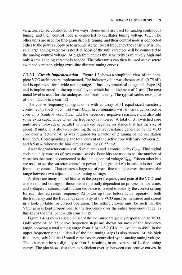
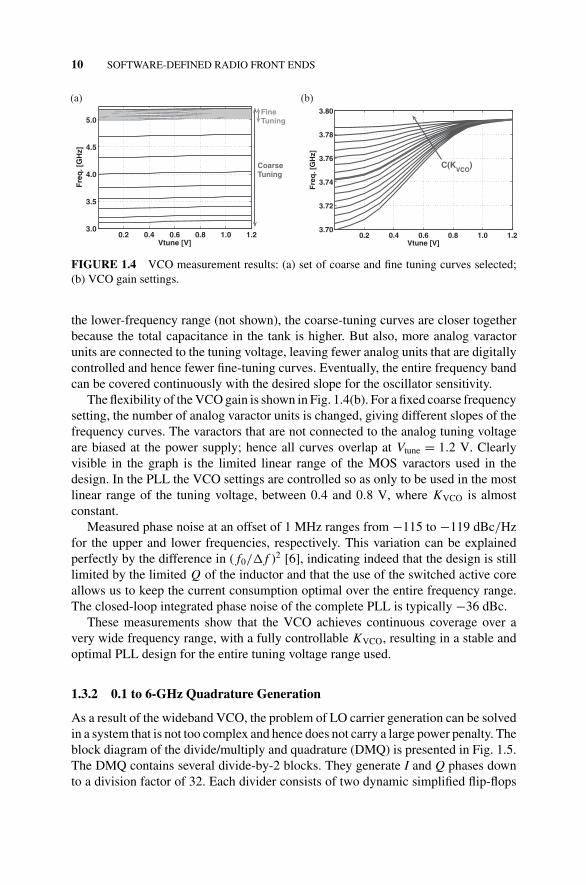
Figure 1.4(a) shows a selected set of the measured frequency response of the VCO.Only some of the 32 coarse frequency steps are shown for most of the frequencyrange, showing a total tuning range from 3.14 to 5.2 GHz, equivalent to 49%. In theupper frequency range, a detail of the fine-tuning steps is also shown. At this highfrequency, only 2 of the 15 small varactors are controlled by the analog tuning voltage.The others can be set digitally to 0 or 1, resulting in an extra set of 14 fine-tuningcurves. The plot shows that there is sufficient overlap between consecutive curves. In
c01 JWBS029-Hueber September 2, 2010 10:26 Printer: Yet to come
10 SOFTWARE-DEFINED RADIO FRONT ENDS
0.2 0.4 0.6 0.8 1.0 1.23.0
3.5
4.0
4.5
5.0
Vtune [V]
Fre
q. [
GH
z]
Fine Tuning
Coarse Tuning
0.2 0.4 0.6 0.8 1.0 1.23.70
3.72
3.74
3.76
3.78
3.80
Vtune [V]
Fre
q. [
GH
z]
C(KVCO
)
(a) (b)
FIGURE 1.4 VCO measurement results: (a) set of coarse and fine tuning curves selected;(b) VCO gain settings.
the lower-frequency range (not shown), the coarse-tuning curves are closer togetherbecause the total capacitance in the tank is higher. But also, more analog varactorunits are connected to the tuning voltage, leaving fewer analog units that are digitallycontrolled and hence fewer fine-tuning curves. Eventually, the entire frequency bandcan be covered continuously with the desired slope for the oscillator sensitivity.
The flexibility of the VCO gain is shown in Fig. 1.4(b). For a fixed coarse frequencysetting, the number of analog varactor units is changed, giving different slopes of thefrequency curves. The varactors that are not connected to the analog tuning voltageare biased at the power supply; hence all curves overlap at Vtune = 1.2 V. Clearlyvisible in the graph is the limited linear range of the MOS varactors used in thedesign. In the PLL the VCO settings are controlled so as only to be used in the mostlinear range of the tuning voltage, between 0.4 and 0.8 V, where KVCO is almostconstant.
Measured phase noise at an offset of 1 MHz ranges from −115 to −119 dBc/Hzfor the upper and lower frequencies, respectively. This variation can be explainedperfectly by the difference in ( f0/� f )2 [6], indicating indeed that the design is stilllimited by the limited Q of the inductor and that the use of the switched active coreallows us to keep the current consumption optimal over the entire frequency range.The closed-loop integrated phase noise of the complete PLL is typically −36 dBc.
These measurements show that the VCO achieves continuous coverage over avery wide frequency range, with a fully controllable KVCO, resulting in a stable andoptimal PLL design for the entire tuning voltage range used.
1.3.2 0.1 to 6-GHz Quadrature Generation
As a result of the wideband VCO, the problem of LO carrier generation can be solvedin a system that is not too complex and hence does not carry a large power penalty. Theblock diagram of the divide/multiply and quadrature (DMQ) is presented in Fig. 1.5.The DMQ contains several divide-by-2 blocks. They generate I and Q phases downto a division factor of 32. Each divider consists of two dynamic simplified flip-flops

c01 JWBS029-Hueber September 2, 2010 10:26 Printer: Yet to come
WIDEBAND LO SYNTHESIS 11
2G4G
4G
4G
1G
DIV2
PPF
BUF
PPF
4G:2
G5G:3G
0.5G
250M
125M
DIV2
DIV2 DIV2 DIV2 DIV2
1.5G
FIGURE 1.5 Block diagram of the DMQ circuit.
in feedback. The rail-to-rail operation of the latches ensures a minimal addition ofphase noise, very important in cellular standards.
The DMQ further employs a single-side band (SSB) mixer. For a VCO at its 4-GHzcenter frequency, the mixer combines 4GHz or 2 GHz with 1 GHz to obtain 5 GHz or3 GHz, respectively. The 2- and 1-GHz components are obtained by division of theVCO frequency. The 4-GHz quadrature phases needed for SSB mixer operation in the5-GHz mode are generated through a polyphase filter (PPF1). This is implemented asa three-stage polyphase filter, with notches at negative frequencies of 3, 4, and 5 GHz.The circuit diagram of the SSB mixer is presented in Fig. 1.6. As both base frequenciesused in the SSB mixing are square waves, they contain all odd harmonics. These arealso combined in the mixer and will generate unwanted frequency components. Tolimit these, the 1-GHz (F1) component is first linearized by filtering out the thirdharmonic of the 1-GHz square wave. This negative frequency is attenuated by 40 dBwith a two-stage polyphase filter with notches at −2 and − 4 GHz. The output ofthis polyphase filter is a current whose four quadrature phases are injected directlyinto the SSB mixer. With the VCO at its center frequency, the mixer’s switches aredriven by either a 2- or 4-GHz rail-to-rail square wave. Cascode transistors belowthe switches provide a low impedant input for the linearized 1-GHz current. The biascurrent is provided by current sources at the bottom. Note that both current sourcesand cascode transistors are common to both the I and Q paths. The output of themixer (F3) is amplified up to full rail swing with a differential pair followed by astring of inverters, of which the first is biased around its threshold voltage.
The SDR’s LO frequency can be selected by a multiplexer integrated in the DMQ.This function is obtained by powering down the unused blocks and placing theiroutputs in a high-impedance state. In this way, no extra circuits are placed in thesignal path.

c01 JWBS029-Hueber September 2, 2010 10:26 Printer: Yet to come
12 SOFTWARE-DEFINED RADIO FRONT ENDS
Gnd
Vdd
Vdd
F3INF3IP
Vdd
F3QN
PPF
F2IF2Q
VC
F3QP
F1I
F1Q
IP
IN
QP
QN
FIGURE 1.6 SSB mixer circuit diagram.
1.4 RECEIVER BUILDING BLOCKS
A key aspect for the receiver RF part is its interference robustness. The blockingrequirements for simultaneous multi-mode operation imply the need for tunablenarrowband circuits at the antenna interface. Either this function can be provided bya multi-band filtering block [9], in which case the receiver’s input can be a widebandlow-noise amplifier, or part of this burden can be taken up in the low-noise amplifier(LNA) design, as shown in the following section.
1.4.1 MEMS-Enabled Dual-Band Low-Noise Amplifier
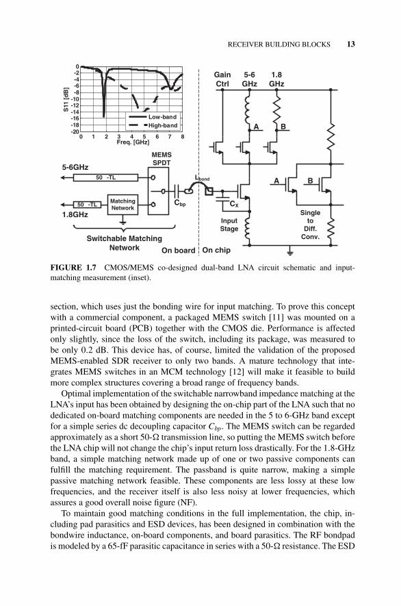
In this first example the option of using microelectromechanical systems (MEMSs)switches to build a low-loss reconfigurable antenna filter section on a thin-film sub-strate is explored. This is especially relevant when simultaneously considering thedesign of the LNA, whose active CMOS part must be co-designed with the MEMSswitch and the passive off-chip matching. The circuit schematic of Fig. 1.7 showshow multi-band operation is achieved independent of the inductive emitter degen-eration [10]. A single-pole dual-throw (SPDT) MEMS switch is used to connectthe LNA to either its 1.8-GHz matching circuit and antenna filter, or to its 5-GHz
c01 JWBS029-Hueber September 2, 2010 10:26 Printer: Yet to come
RECEIVER BUILDING BLOCKS 13
On board On chip
InputStage
GainCtrl
50 -TL
5-6GHz
50 -TL
1.8GHz
MatchingNetwork
MEMSSPDT
Switchable MatchingNetwork
Lbond
5-6GHz
1.8GHz
BA
BA
Singleto
Diff.Conv.
Cbp CX
0 1 2 3 4 5 6 7 8-20-18-16-14-12-10-8-6-4-20
Low-bandHigh-band
Freq. [G
S11
[dB
]
Hz]
FIGURE 1.7 CMOS/MEMS co-designed dual-band LNA circuit schematic and input-matching measurement (inset).
section, which uses just the bonding wire for input matching. To prove this conceptwith a commercial component, a packaged MEMS switch [11] was mounted on aprinted-circuit board (PCB) together with the CMOS die. Performance is affectedonly slightly, since the loss of the switch, including its package, was measured tobe only 0.2 dB. This device has, of course, limited the validation of the proposedMEMS-enabled SDR receiver to only two bands. A mature technology that inte-grates MEMS switches in an MCM technology [12] will make it feasible to buildmore complex structures covering a broad range of frequency bands.
Optimal implementation of the switchable narrowband impedance matching at theLNA’s input has been obtained by designing the on-chip part of the LNA such that nodedicated on-board matching components are needed in the 5 to 6-GHz band exceptfor a simple series dc decoupling capacitor Cbp. The MEMS switch can be regardedapproximately as a short 50-� transmission line, so putting the MEMS switch beforethe LNA chip will not change the chip’s input return loss drastically. For the 1.8-GHzband, a simple matching network made up of one or two passive components canfulfill the matching requirement. The passband is quite narrow, making a simplepassive matching network feasible. These components are less lossy at these lowfrequencies, and the receiver itself is also less noisy at lower frequencies, whichassures a good overall noise figure (NF).
To maintain good matching conditions in the full implementation, the chip, in-cluding pad parasitics and ESD devices, has been designed in combination with thebondwire inductance, on-board components, and board parasitics. The RF bondpadis modeled by a 65-fF parasitic capacitance in series with a 50-� resistance. The ESD

c01 JWBS029-Hueber September 2, 2010 10:26 Printer: Yet to come
14 SOFTWARE-DEFINED RADIO FRONT ENDS
diodes are sized 2 × 0.6 µm × 12 µm each and have in total a 60-fF parasitic capac-itance. Each bondwire is modeled by a 1.3-nH inductance. PCB traces are modeledas small transmission lines when needed. Surface-mounted components on the boardare characterized carefully with dedicated separate deembedding structures.
An extra on-chip capacitor CX connecting the gate and source of the input transis-tor reduces the gate inductance needed for the input matching to a value of 1.3 nH at5 GHz, which is conveniently implemented as a bonding wire. Otherwise, this induc-tance can be unrealistically large and the Q-factor of the input resonance network ofthe LNA would be too high to cover a 1-GHz band. Thanks to the 300-fF capacitance,the gate inductance can be implemented with a single bonding wire.
Internally, the LNA has two separate outputs to cover the required frequency range.A resistively loaded output is, of course, small in area and flexible in terms of widebandwidth but can only provide enough gain at frequencies up to 2.5 GHz, due tothe limitation of the 0.13-µm CMOS technology used. Therefore, a second output isadded for the 5 to 6-GHz band with an LC-tuned load, and the selection of either oneof those is done by proper biasing of the cascode transistors. A resistor in parallelwith this inductor lowers its quality factor and hence increases its bandwidth in orderto cover the 1-GHz bandwidth.
Gain switching is achieved by the current steering technique, when the thirdcommon-gate transistor is activated, which bypasses a certain fraction of the signalcurrent to the power supply so as to reduce the gain. Finally, both outputs pass througha multiplexing single-to-differential converter.
The input stage is biased at 5.8 mA, and another 3.6 mA is used in the secondstage, for an overall gain of 24 dB. As indicated in Fig. 1.7, S11 input matching betterthan −10 dB is achieved in both bands. The simulated LNA NF is around 2 dB, whilethe IIP3 value is −5 dBm in the low band and 3 dBm in the high band.
1.4.2 Wideband Low-Noise Amplifiers
Another option to demonstrate the SDR concept is to rely completely on the passivesin the antenna interface for RF interference and blocking filtering. This makes therealization of the concept easier, as commercially available (multi-band) filteringblocks can be used in the implementation. Wideband low-noise amplifiers must nowbe used that cover an RF frequency range as large as possible for optimal flexibility,but on the other hand must still achieve state-of-the-art performance with respect tonarrowband LNAs.
Covering the full 100 MHz to 6 GHz frequency range is challenging since achiev-ing a low NF at hundreds of megahertz requires large transistors with low 1/ fnoise, while moving toward carrier frequencies of a few gigahertz requires fast tran-sistors. Recently, several 90-nm wideband inductor-less feedback LNAs have beenreported [13]. However, none of them achieved the performance targeted by a linkbudget analysis for an SDR-LNA below 500 MHz (for a 1.2-V power supply).LC-matched common-source (CS) LNAs typically cover a bandwidth from 3 to10 GHz [14]. Extending the bandwidth down to 100 MHz would require prohibitivelylarge inductors and thus chip area.