flowing venture capital where it’s needed pg
DESCRIPTION
EDN Magazine 26 Nov 2009TRANSCRIPT

VOICE OF THE ENGINEER
Issue 21/2005www.edn.com
Flowing venture capital where it’s
needed Pg 13
H-1B visa program Pg 6
Baker’s Best Pg 14
Prying Eyes: Solar Vision Pole Pg 16
Design Ideas Pg 42
Tales from the Cube Pg 52
26Issue 22/2009
www.edn.com
®
NOV
( )
LESSONS FROM THE LAST MILE Page 18
FROM MAGNETIC TO SOLID STATE, SPIN-FREE: WHAT A LONG, STRANGE STORAGE TRIP IT’S TURNING OUT TO BE Page 24
EVALUATING ESD-PROTECTION COMPONENTS Page 33
MAGNETICS IN SWITCH- MODE POWER SUPPLIES Page 36
edn091102covDIGITAL_id 00C1edn091102covDIGITAL_id 00C1 11/13/2009 1:02:05 PM11/13/2009 1:02:05 PM

A division of
Get free advice, pricing articles, ratings and quotes on Business Purchases from digital copiers,to phone systems, to payroll services and more. Visit BuyerZoneBusiness.com today to makefast and efficient business purchase decisions. At BuyerZone, you’re in control. We’re just hereto make your work easier.
Join the millions who’ve already saved time and money on many of their Office Equipmentpurchases by taking advantage of BuyerZone’s FREE, no obligation services like:• Quotes from multiple suppliers• Pricing articles• Buyer’s guides• Supplier ratings• Supplier comparisons
REQUEST FREE QUOTES NOW!Call (866) 623-5564 or visit BuyerZoneBusiness.com Where Smart Businesses Buy and Sell
No need to duplicate yourself
BuyerZone saves you time and moneyon COPIERS AND MORE.
EDN091102covers.indd 00C2EDN091102covers.indd 00C2 11/5/2009 1:45:13 PM11/5/2009 1:45:13 PM

Enter xx at www.edn.com/info
edn091102.indd 1edn091102.indd 1 11/5/2009 1:50:59 PM11/5/2009 1:50:59 PM
×
•
42 Inspect solar cells without a microscope
43 Solar-powered sensor controls traffic
46 Self-oscillating H bridge lights white LED from one cell
48 Low-cost LCD-bias generator uses main microcontroller as control IC
J4
P3
CP24 nF
CAP PAD
4
3
2
1
10-mSEC MINIMUM PULSE30-mV CAPACITIVE SENSOR
D11N5333
Q1
R14100k
R152k
C1220
ESD
863-1N5228BG
RC=100 �SEC
D
G
S QMN-2N
D E S I G N I D E A S
From magnetic tosolid state, spin-free:What a long, strangestorage trip it’s turningout to be
24To seriously competewith hard-drive mak-ers, semiconductor
vendors must amass a robust,sustained supply of silicon forsolid-state drives. They also mustaddress plenty of misconceptionsabout the newer technology’scapabilities and limitations.
by Brian Dipert, SeniorTechnical Editor
Evaluating ESD-pro-tection components:Clamping voltage anddynamic resistance arecrucial
33A changing product land-scape and new designs call
for improved protection againstESD strikes on components. Alow-voltage device doesn’t nec-essarily have greater protection.Protection comes from low clamp-ing voltage and low dynamicresistance. by Chi T Hong,
California Micro Devices
11.26.09
contents
Lessons fromthe last mile
18Chip designers’ strugglesto provide triple-play HD
service to telephone, cable, andwireless customers are changingthe nature of SOC architecture.
by Ron Wilson, Executive Editor
9 WinSystems highlightsAtom board, CompactFlash
10 High-performance MSOsfeature 20-GHz analogbandwidth
11 Stable quartz oscillator usesSAW technology
11 Cortex-M3 microcontrollercuts energy consumption
12 China’s proposed ban of rare-earth metals would affecthybrid cars, CFLs
12 Online-power-supply designtool evaluates 48 billiondesigns
13 Voices: Tim Draper: flow-ing venture capital where it’sneeded
Dilbert 10pulse
2 EDN | NOVEMBER 26, 2009
What every designershould know aboutmagnetics in switch-mode power supplies
36Power is often an after-thought in system design,
but the choice and design of themagnetic elements at the heart ofan SMPS are crucial. Acquaint orreacquaint yourself with the fun-damentals of this frequently over-looked area.
by Sameer Kelkar, Power Integrations
edn091102toc_id 2edn091102toc_id 2 11/12/2009 11:21:33 AM11/12/2009 11:21:33 AM

www.coilcraft.com 800/322-2645
®
RoHSCOMPLIANT
®
IC reference designs area good start. But what ifyou want to optimize thedriver inductor for size,efficiency or price?
Or evaluate newer,high performance partsthat weren’t availablewhen the reference design was created?
Then you’ll want to check out the new
LED Design Center on theCoilcraft web site. It’s filledwith interactive tools thatlet you compare hundreds ofinductors for all LED drivertopologies, including SEPIC.
To start yoursearch for the per-
fect LED driver inductor, mouseover to www.coilcraft.com/LED
Our new LED Design Center lets you:d Search by IC to find all matching inductorsd Compare DCR, current rating, size and price
d Analyze all core and winding lossesd Request free evaluation samples
www.coilcraft.com/LED
How to pick the perfect inductorfor your LED driver application
7.875 x 10.5
edn091102.indd 3edn091102.indd 3 11/5/2009 1:51:03 PM11/5/2009 1:51:03 PM

www.mouser.comOver A Million Products Online
The NewestOptoelectronics
Experience Mouser’s time-to-marketadvantage with no minimums and same-dayshipping of the newest products from morethan 390 leading suppliers.
(800) 346-6873
The Newest Products For Your Newest Designs
The ONLY New Catalog Every 90 Days
New Products from:
IR OSTAR® Infrared LEDswww.mouser.com/osramirostar
40W LED Emitterwww.mouser.com/ledengin40w
QuasarBrite™ Narrow BeamLEDswww.mouser.com/lumex_quasarbrite
ASMT-Jx1x 1W Mini Power LEDLight Sourcewww.mouser.com/avago1wminiled
edn091102.indd 4edn091102.indd 4 11/5/2009 1:51:04 PM11/5/2009 1:51:04 PM
EDN® (ISSN#0012-7515), (GST#123397457) is published biweekly, 24 times per year, by Reed Business Information, 8878 Barrons Blvd, HighlandsRanch, CO 80129-2345. Reed Business Information, a division of Reed Elsevier Inc, is located at 360 Park Avenue South, New York, NY 10010.John Poulin, CEO/CFO, RBI-US; Jeff DeBalko, President, Business Media; Jane Volland, Vice President, Finance. Periodicals postage paid at Littleton,CO 80126 and additional mailing offices. Circulation records are maintained at Reed Business Information, 8878 S Barrons Blvd, Highlands Ranch,CO 80129-2345. Telephone (303) 470-4445. POSTMASTER: Send address changes to EDN®, PO Box 7500, Highlands Ranch, CO 80163-7500.EDN® copyright 2009 by Reed Elsevier Inc. Rates for nonqualified subscriptions, including all issues: US, $179.99 one year; Canada, $229.99 one year(includes 7% GST, GST#123397457); Mexico, $229.99 one year; air expedited, $399.99 one year. Except for special issues where price changes areindicated, single copies are available for $10 US and $15 foreign. Publications Agreement No. 40685520. Return undeliverable Canadian addressesto: RCS International, Box 697 STN A, Windsor Ontario N9A 6N4. E-mail: [email protected]. Please address all subscription mail to EDN®,8878 S Barrons Blvd, Highlands Ranch, CO 80129-2345. EDN® is a registered trademark of Reed Elsevier Properties Inc, used under license. A ReedBusiness Information Publication/Volume 54, Number 22 (Printed in USA).
6 EDN.comment: Weak economy, anti-immigrant sentimenthit H-1B visa program
14 Baker’s Best: Understanding CMR and instrumentation amplifiers
16 Prying Eyes: Visionaire Lighting’s Solar Vision Pole:shedding light on off-grid lampposts
50 Product Roundup: Optoelectronics/Displays
52 Tales from the Cube: Hawk eyes, analog equipment trumpexpensive digital test set
16 52
O N L I N E O N LYCheck out these Web-exclusive articles:
online contents www.edn.com
contents 11.26.09
D E PA R T M E N T S & C O L U M N S
IR’s AC-DC product portfolio offers simple, compact high
density solutions tailoredfor energy-effi cient
power supplies.
Simpler PowerConversion
THE POWER MANAGEMENT LEADER
For more information call1.800.981.8699 or visit
www.irf.com
PartNumber Pckg. VCC
(V)Freq.(kHz)
GateDrive±(A)
VGATEClamp
(V)
CurrentMode
IR1150(STR)PbF
SO-8PDIP8 13-22 50-200 1.5 13 CCM
PartNumber
IR1166SPbF
IR1167ASPbF
IR1167BSPbF
IR1168SPbF
Package SO-8
VCC (V) 20
VFET (V) <=200
Sw Freq.max (kHz) 500
Gate Drive ±(A) +1/-4 +2/-7 +1/-4
VGATE Clamp (V) 10.7 10.7 14.5 10.7
Min. On Time (ns) Program. 250 -3000 750
Channel 1 2
RoHS
μPFC™ PFC IC
SmartRectifier™ IC
Specify an external reference clockto improve SERDES performanceVarious serial data standards requiredifferent clock specifications.➔www.edn.com/article/CA6703242
Oscilloscope probe accessories—It’s the little things that matterProbe accessories, including tips, caps, adapt-ers, springs, positioners, clips, and hooks,can help you conveniently make accuratemeasurements.➔www.edn.com/article/CA6704367
Visit www.edn.com and● Sign up for our free newslettersor to receive your subscriptiondigitally
● Check out our Hot Topics to getall the information you need aboutwhat’s HOT right now
● Check out the News Center,which provides up-to-the-minutenews, analysis, research, and insighton the global electronics industry
● Check out the Design Centers,which feature articles, new-productinformation, and valuable designresources in several areas
and much, much more!
WHAT’S UP AT EDN.COM
Nominations for the 20th annualInnovation Awards
WANTED NOW!
www.edn.com/innovation
INNO ATION
edn091102toc_id.indd 5edn091102toc_id.indd 5 11/12/2009 11:51:00 AM11/12/2009 11:51:00 AM
6 EDN | NOVEMBER 26, 2009
BY RICK NELSON, EDITOR-IN-CHIEF
,,E D N . C O M M E N T
The article notes that, in additionto the weak economy, rising anti-im-migrant sentiment in Washington andthe higher costs of hiring foreign-bornworkers are also taking their toll on thevisa program. Indian outsourcing com-panies such as HCL have traditionallybeen the largest recipients of H-1B vi-sas, according to the article, but HCLhas been hiring Americans who other-wise may have faced layoffs from com-panies switching work to HCL.
Would-be immigrants are also find-ing more opportunities at home. Thearticle quotes Vivek Wadhwa, a schol-ar who has studied H-1B visas, as say-ing, “The best and the brightest whowould normally come here are say-ing, ‘Why do we need to go to a coun-try where we are not welcome, … ourquality of life would be less, and wewould be at the bottom of the socialladder?’”
I commented on the trend for for-eign nationals to stay home when Ireported on a study Wadhwa conduct-ed for the Ewing Marion KauffmanFoundation (references 2 and 3). Thestudy notes that immigrant-found-ed US-based companies employed450,000 workers and generated $52billion in revenue in 2006. The WSJarticle quotes Microsoft general coun-
cil Brad Smith as saying that 35% ofMicrosoft’s US patent applications lastyear came from new inventions by visaand green-card holders.
“While some have tried to associ-ate the increase in foreign workers ...with the economic problems that haveplagued the country, this data veri-fies the opposite effect,” said Wad hwawhen the Kauffman Foundation re-leased its study. “If the US governmentand the business community could findbetter ways to offer good jobs in tan-dem with less restrictive visa policiesfor talented immigrants, the UnitedStates might be able to recapture manyof these immigrants and their potentialto help grow the US economy.”
Companies such as Microsoft thatbenefit from the visa program
contend that the currentslump in the program
demonstrates that the mar-ket, not Congress, should de-termine how many immigrants
should be allowed to work in the Unit-ed States. The WSJ article quotes Jeni-fer Verdery, director of work-force pol-icy at Intel, as saying that the fact thatthe cap hasn’t been reached this yearshows that the market will temperdemand.
There seems to be bipartisan dis-agreement in Congress with that po-sition. As the WSJ reports, SenatorCharles Grassley, an Iowa Republi-can, wrote a letter to the new direc-tor of citizenship and immigration ser-vices, urging tighter controls on H-1Bvisas. In April, Grassley and IllinoisDemocrat Senator Richard Durbin in-troduced legislation to require compa-nies to pass more stringent labor-mar-ket tests that would ensure they makea bigger effort to hire US workers.
The H-1B visa program is valuable,and, as the Kauffman Foundation studypoints out, immigrants have contribut-ed disproportionately to the US econo-my’s high-tech sector. If Americans areunwilling or unable to contribute theirfair share, then it will be important toUS economic success to attract talentfrom overseas. There is a role for Con-gress to play to provide further safe-guards so that cheaper workers fromabroad don’t displace motivated, quali-fied Americans. If Congress can ensureAmericans that the program works asintended, political support for expand-ing the program might grow.EDN
R E FE R E N CE S1 Jordan, Miriam, “Slump Sinks VisaProgram,” The Wall Street Journal, Oct30, 2009, http://online.wsj.com/article/SB125677268735914549.html.2 Nelson, Rick, “Immigrant brain-drainchallenges US innovation,” Test &Measurement World, March 2, 2009,www.edn.com/091126eda.3 Wadhwa, Vivek, et al., “America’sLoss is the World’s Gain,” Ewing Mar-ion Kauffman Foundation, March2009, www.kauffman.org/uploadedfiles/americas_loss.pdf.
Contact me at [email protected].
The woeful employment picture in the United States is result-ing in thousands of unfilled spots in the H-1B visa programfor the first time since 2003, according to a recent article inThe Wall Street Journal (Reference 1). Although employers injust one day snapped up all 65,000 available visas, would-beimmigrants filed only 46,700 petitions for employment as of
Sept 25—about six months after employers scooped up the visas.
Weak economy, anti-immigrantsentiment hit H-1B visa program
edn091102ed_id 6edn091102ed_id 6 11/11/2009 10:35:31 AM11/11/2009 10:35:31 AM

RELIABILITY
www.mill-max.com/EDN596
MAXIMUMIn contact, stability and low-noise performanceMill-Max Mfg. Corp. spring-loaded connectors provide superior reliability under the most rigorous environmental conditions, offering:
Stay in contact withMill-Max spring-loaded connectors.
offerings and request a datasheet
EDN. 225 Wyman St, Waltham, MA 02451. www.edn.com. Phone 1-781-734-8000.Address changes or subscription inquiries: phone 1-800-446-6551; fax: 1-303-470-4280; [email protected]. For a free subscription, go to www.getfreemag.com/edn. Reed Business Information, 8878 S Barrons Blvd, Highlands Ranch, CO 80129-2345. Include your mailing label.
PUBLISHER, EDN WORLDWIDERussell E Pratt, 1-781-734-8417;
ASSOCIATE PUBLISHER,EDN WORLDWIDE
Judy Hayes, 1-925-736-7617;[email protected]
EDITOR-IN-CHIEF, EDN WORLDWIDERick Nelson, 1-781-734-8418;
EXECUTIVE EDITORRon Wilson, 1-510-744-1263;
MANAGING EDITORAmy Norcross
1-781-734-8436;fax: 1-720-356-9161;
[email protected] for contributed technical articles
SENIOR ART DIRECTORMike O’Leary
1-781-734-8307;fax: 1-303-265-3021;
ANALOGPaul Rako, Technical Editor
1-408-745-1994;[email protected]
MASS STORAGE, MULTIMEDIA,PCs, AND PERIPHERALS
Brian Dipert, Senior Technical Editor1-916-760-0159;
fax: 1-303-265-3187;[email protected]
MICROPROCESSORS, DSPs,AND TOOLS
Robert Cravotta, Technical Editor1-661-296-5096;
fax: 1-303-265-3116;[email protected]
NEWSSuzanne Deffree, Managing Editor
1-631-266-3433;[email protected]
POWER SOURCES,ONLINE INITIATIVES
Margery Conner, Technical Editor1-805-461-8242;
fax: 1-805-461-9640;[email protected]
DESIGN IDEAS EDITORMartin Rowe,
Senior Technical Editor,Test & Measurement World
SENIOR ASSOCIATE EDITORFrances T Granville1-781-734-8439;
fax: 1-303-265-3131;[email protected]
EDITORIAL/WEB PRODUCTIONDiane Malone, Manager
1-781-734-8445; fax: 1-303-265-3024Steve Mahoney,
Production/Editorial Coordinator1-781-734-8442; fax: 1-303-265-3198
Melissa Annand,Web Operations Specialist
1-781-734-8443; fax: 1-303-265-3279Adam Odoardi, Prepress Manager
1-781-734-8325; fax: 1-303-265-3042
CONSULTING EDITORJim Williams, Staff Scientist,
Linear Technology
CONTRIBUTING TECHNICAL EDITORSDan Strassberg,
[email protected] Cravotta,
COLUMNISTSHoward Johnson, PhD, Signal Consulting
Bonnie Baker, Texas InstrumentsPallab Chatterjee, SiliconMap
PRODUCTIONDorothy Buchholz,
Group Production Director1-781-734-8329
Joshua S Levin-Epstein,Production Manager
1-781-734-8333; fax: 1-781-734-8096
EDN EUROPEGraham Prophet, Editor, Reed Publishing
+44 118 935 1650;[email protected]
EDN ASIALuke Rattigan, Chief Executive Officer
[email protected] Varma, Editor-in-Chief
EDN CHINAWilliam Zhang,
Publisher and Editorial [email protected]
Jeff Lu, Executive [email protected]
EDN JAPANKatsuya Watanabe, [email protected] Amemoto, [email protected]
PRESIDENT, BUSINESS MEDIA, REED BUSINESS INFORMATIONJeff DeBalko, [email protected]
1-646-746-6573
edn091102edmast_id.indd 7edn091102edmast_id.indd 7 11/11/2009 2:30:24 PM11/11/2009 2:30:24 PM

edn091102.indd 8edn091102.indd 8 11/5/2009 1:51:13 PM11/5/2009 1:51:13 PM

NOVEMBER 26, 2009 | EDN 9
pulseWinSystems has announced its EBC-
Z8510-G single-board computer,which includes an Intel (www.intel.
com) Atom processor. The device measures203�147 mm and supports the new SUMIT-ISM (stackable-unifi ed-modular-interconnect-technology-industry-standard-module)-I/O-expansion standard plus COMIT (computer-on-module interconnect technology), which theSFF-SIG (Small Form Factor Special InterestGroup, www.sff-sig.org) defi nes.
The $795 EBC-Z530-G includes an arrayof onboard peripherals and expansion options.It uses either a 1.1-GHz or a 1.6-GHz Atomand the SCH (system-controller hub)-US15Wwith 512 Mbytes or 1 Gbyte of DDR2 systemmemory. The EBC-Z510-G’s I/O interfacefeatures two GbE (gigabit-Ethernet) ports,CRT and LVDS (low-voltage-differential-sig-naling) fl at-panel video, a MiniPCIe (PeripheralComponent Interconnect Express)-card inter-face for a wireless-networking module, fourUSB (Universal Serial Bus) 2.0 ports, fourserial COM ports, HD (high-defi nition) audio,a PATA (parallel-advanced-technology-attach-ment) controller for both a CompactFlash anda hard disk, 48 lines of digital I/O, a parallelprinter port, and a PS/2 port. Two SUMIT andlegacy PC/104 connectors support additionalI/O-module expansion. The ROHS (reduction-of-hazardous-substances)-compliant boardoperates over an industrial temperature rangeof �40 to �70�C for processor- and I/O-intensive applications in harsh environments.
Because the EBC-Z510-G’s architectureis PC-compatible, it supports Windows XPembedded and Linux operating systems alongwith a software-development tool set thatincludes device drivers and libraries. It alsosupports advanced features, such as a custom
splash screen, APM (advanced-power-man-agement) and ACPI (advanced-confi guration-and-power-interface) modes, and PXE (pre-boot execution environment).
According to WinSystems’ vice president,Robert Burkle, the EBC-Z510-G is the fi rstboard to support COMIT, which targets use inSFF processor modules and baseboards. Thecompany uses a 62�75-mm SFF-COM card,which is roughly the size of a credit card, thatincludes the Atom, SCH, memory, and powersupplies. For more on this introduction, go towww.edn.com/article/CA6699174.
—by Rick Nelson�WinSystems, www.winsystems.com.
WinSystems highlightsAtom board, CompactFlash
EDITED BY FRAN GRANVILLE
“The debunkerdog in you shouldget busy. … If I’mwrong I’ll eat mywords (or breathethe fumes—what-ever).”—Engineer Meredith Poor, inEDN’s Feedback Loop, at www.edn.com/article/CA6670951.Add your comments.
FEEDBACK LOOP
INNOVATIONS & INNOVATORS
WinSystems’ EBC-Z8510-Gincludes an Intel Atom processor on a203�147-mm board. It supports SUMIT-ISMand COMIT, which the SFF-SIG defines.
edn091102pulse_id 9edn091102pulse_id 9 11/11/2009 2:58:19 PM11/11/2009 2:58:19 PM

Tektronix has announcedthe MSO70000 series ofMSOs (mixed-signal os-
cilloscopes). The instrumentscan capture as many as 20channels of data—four analogwith bandwidth ranging from 4to 20 GHz, depending on themodel, and 16 digital with tim-ing resolution of 80 psec onall models. Memory depths to250M points are available onall channels of all models.
The MSO70000 combines afull suite of measurement capa-bilities that help resolve analogissues in digital systems. Youcan use the instruments to de-bug and verify in such demand-ing, high-speed design applica-tions as DDR memory, high-performance ASICs, FPGAs,SOCs (systems on chips), anddigital RF. The MSO70000 of-fers a variety of probing acces-sories for making minimallydisruptive analog and digitalconnections to a DUT (deviceunder test).
The instruments deliver ad-vances in the discovery of prob-lems, capture of notable events,quick searches through longrecords to reveal the capturedevents, and analysis to obtainrapid insight into the causes ofanomalous DUT behavior. Thedevices offer as much as fi vetimes the bandwidth and timingresolution of the fastest-avail-
able integrated MSOs.Maximum sample rates are
50G samples/sec on analogchannels and 12.5G samples/sec on digital channels. To mini-mize confusion, the analog- anddigital-record durations alwaysmatch; the scopes add repeat-ed samples to the channelsthat are acquiring at the lowerrate so that analog and digitalrecords always contain equalnumbers of samples. This fea-
ture allows you to capture long-duration events with high sam-ple resolution and obtain time-correlated views of high-speedanalog and digital data.
The MSO70000 series pro-vides a comprehensive set ofinnovative solder-in probe ac-cessories that simplify con-necting to vias and fi ne-pitchcomponents on tightly packedboards to acquire such sig-nals as those on the digi-
tal-control lines of the DDRcommand bus. The tool setfor DDR probing now also in-cludes new BGA interposersfor all variants of DDR3- andDDR2-memory componentsand provides access to all sig-nals with excellent fi delity. Theunits work with the company’siCapture technology, which al-lows internal routing of select-ed digital signals to the analogchannels for full analog evalu-ation, making the MSO70000ideal for highly sensitive, fi ne-pitch board layouts.
The iCapture feature offersanalog views of any connecteddigital channel, providing de-bugging insight across all 20channels. The series providesserial-pattern, mixed analogand digital, logic-pattern, andbus-state triggers, which youcan combine to isolate systemfaults that occur only duringparticular system states. Theunits provide tight timing syn-chronization between the ana-log and the digital subsystems.Timing correlation as close as80 psec is possible, result-ing in easier determination ofthe cause and effect of circuitbehavior.
More than 30 analysis suitesrun on the series. You can se-lect from the new I2C (inter-in-tegrated-circuit) and SPI (se-rial-peripheral-interface) bus-analysis tools, DPOjet (digital-phosphor oscilloscope jet) forjitter and eye-diagram analy-sis, DDRA (DDR analysis) forDDR-memory-bus verifi cation,SDLA (serial-data-link analy-sis) for equalized-channel em-ulation and analysis, and Sig-nalVu for frequency-domaindisplay and analysis. The man-ufacturer’s suggested US re-tail prices for the MSO70000units start at $67,400.
—by Dan Strassberg�Tektronix Inc, www.tektronix.com.
10 EDN | NOVEMBER 26, 2009
pulseHigh-performance MSOs feature20-GHz analog bandwidth
On each of their four analog channels, MSO70000 series instru-ments offer five times the bandwidth of other MSOs. Each ofthe 16 differential-input digital channels provides 80-psec timingresolution and up to 250M samples of capture memory.
DILBERT By Scott Adams
edn091102pulse_id 10edn091102pulse_id 10 11/11/2009 2:58:25 PM11/11/2009 2:58:25 PM

NOVEMBER 26, 2009 | EDN 11
Targeting LANs (local-area networks) and SAN(storage-area networks),
Epson Toyocom recentlyannounced the highly stableEG-4101/4121CA SAW (sur-face-acoustic-wave) resonator.The part combines low jitter,low phase noise, high stability,and temperature coeffi cientsbetter than those of AT-cut
quartz crystals. The resonatoroffers a frequency toleranceof �50 ppm and maximumphase jitter of 0.2 psec at 622MHz over a 12-kHz to 20-MHzbandwidth. The device is avail-able with LV-PECL (low-volt-age-positive-emitter-coupled-logic), LVDS (low-voltage-dif-ferential-signaling), and HCSL(high-speed-current-steer-
ing-logic) outputs. Availablefrequency ranges are 100 to700 MHz for the LV-PECL-and LVDS-output versionsand 100 to 500 MHz for theHCSL version. The resonatorhas a supply voltage of 2.5 to3.3V, and current consumptionranges from a maximum of 30or 45 mA over the supply-volt-age range for the LVDS version
to 80 or 100 mA for the LV-PECL version.
SAW resonators and oscil-lators differ from SAW fi ltersin that the resonators use aquartz rather than a ceramicelement. Don’t confuse SAWresonators with inexpen-sive silicon or ceramic reso-nators, which tend to have amuch lower Q (quality fac-tor) and worse initial accuracyand temperature coeffi cients.Because the SAW resonatorsoperate at their fundamental-resonance mode, they lack thefrequency jitter of conventionalcrystal oscillators that operateat a lower frequency; a PLL(phase-locked loop) then mul-tiplies that frequency inside thechip. The operation at funda-mental mode also means thatthe parts do not frequency-hopas quartz crystals do.
The EG-4101/4121CA de-vice operates over a standardtemperature range of �40 to�85�C or an optional range of�40 to �90�C and comes in a7�5�1.2-mm package. It sellsfor $12 to $18 (1000) and isavailable for sampling now.
—by Paul Rako�Epson Toyocom, www.epsontoyocom.co.jp/english.
Stable quartz oscillator usesSAW technology
The EG-4101/4121CA series of SAW oscillators from Epson has a flat frequency variation overtemperature.
CORTEX-M3 MICROCONTROLLER CUTS ENERGY CONSUMPTION
11.2
6.09
Energy Micro’s new EFM32G Gecko microcontroller fam-ily sports an energy-efficient implementation of a 32-bitARM (www.arm.com) Cortex-M3-microcontroller architec-ture. The family thus targets applications, such as meters,requiring extended battery life. The devices support fivepower modes with an operating voltage range of 1.8 to3.8V. Active-mode current consumption is as low as 180�A/MHz at 3V when executing code from flash memory.Standby current consumption is 900 nA at 3V with areal-time clock, a 32.768-kHz oscillator, power-on reset,brownout detection, and full RAM and CPU retention.Deep-sleep-mode current draw is 20 nA at 3V, and wake-up time from sleep mode is as fast as 2 �sec.
The 32-MHz microcontroller configurations includeas much as 128 kbytes of on-chip flash and 16 kbytes ofRAM. Low-power components include a 200-�A, eight-channel, 12-bit, 1M-sample/sec ADC; a 100-nA brownout
detector; a 50-nA, 32-kHz real-time counter; a 100-nA-re-ceive-mode, 9600-bps-capable UART; and a 50-nA watch-dog timer with dedicated RC oscillator. The ADC supportssingle-ended or differential operation. The 12-bit, 500k-sample/sec DAC supports two single-ended channels orone differential channel. As many as two analog com-parators are available with support for capacitive sens-ing with as many as eight inputs. As many as 90 GPIOs(general-purpose input/outputs) support a 20-mA drivestrength. Hardware AES (Advanced Encryption Standard)with 128/256-bit encryption and decryption is available.The configurable LCD controller can drive an array of4�40 segments.
Prices for the 32-pin devices start at $1.55 (100,000).For more details on this series, go to www.edn.com/article/CA6704374.—by Robert Cravotta�Energy Micro, www.energymicro.com.
edn091102pulse_id 11edn091102pulse_id 11 11/11/2009 2:58:26 PM11/11/2009 2:58:26 PM

12 EDN | NOVEMBER 26, 2009
China’s Ministry of In-dustry and InformationTechnology is propos-
ing a total ban on exports ofterbium, dysprosium, yttrium,thulium, and lutetium and a re-striction on neodymium, euro-pium, cerium, and lanthanumto a total of 35,000 tons ayear, which is far below glob-al needs. Many of these met-als are vital to energy-effi cienttechnology. For example, neo-dymium fi nds use in rare-earthmagnets for high-efficiencymotors, and new front-loadingclothes washers use rare-earthmagnets in their motors.
According to a recent ar-ticle (Reference 1), “No re-placement has been found
for neodymium that enhancesthe power of magnets at highheat and is crucial for hard-diskdrives, wind turbines, and theelectric motors of hybrid cars.Each Toyota Prius uses 25pounds of rare-earth elements.Cerium and lanthanum areused in catalytic converters fordiesel engines.” Manufacturersuse terbium in the phosphorsof CFLs (compact fl uorescentlights) to tweak their light to amore pleasant spectrum.
China is currently the on-ly producer of some of thesemetals, so the country’s re-striction or banning of its ex-ports will affect energy-effi -cient products worldwide. Ac-cording to the article, China’s
intent is not to hold the restof the world hostage; Chinaneeds these metals for its in-ternal consumption.
China put many global com-petitors in rare-earth miner-als out of business in the early1990s by fl ooding the market,leading to the closure of thebiggest US rare-earth mine, inMountain Pass, CA, which Mo-
lycorp Minerals operates. Themine is one of the world’s largestand richest rare-earth deposits,and the company is producing avariety of green elements there.It plans to bring the facility backinto full production and re-es-tablish domestic manufacturingcapacity.
—by Margery Conner�Molycorp Minerals, www.molycorp.com.
R E FE R E N CEEvans-Pritchard, Am-
brose, “World faces hi-techcrunch as China eyes banon rare metal exports,”Telegraph, Aug 24, 2009,www.telegraph.co.uk/finance/comment/ambroseevans_pritchard/6082464/World-faces-hi-tech-crunch-as-China-eyes-ban-on-rare-metal-exports.html.
pulseChina’s proposed ban of rare-earthmetals would affect hybrid cars, CFLs
Neodymiumis crucial for
hard-disk drives,wind turbines,and the elec-tric motors ofhybrid cars.
11.2
6.09National Semiconductor
has made significantimprovements to its freeWebench online-designtool, which operates withmost popular Web brows-ers. You access the toolusing a one-time transferof a database in flash for-mat to your computer. Thetool provides a speedyresponse as you experi-ment with various designconfigurations. It includesthe new Visualizer tool tochart efficiency, footprint,and cost variables. Anoptimizer dial lets youestablish your preferencefor trade-offs amongfootprint, efficiency, andcost.
You set a dial thatcauses the tool to gener-ate 50 to 70 designs from48 billion combinationsand to select from 25power-supply topologies,
including buck, boost,buck-boost, SEPIC(single-ended-primary-inductance converter),and flyback. The toolhas a database of 21,000components from 110manufacturers and is suit-able for designs with in-
put voltages of 1 to 100V,output voltages of 0.6 to300V, and power as highas 300W. It can help youdesign for efficiency ashigh as 96% and switch-ing frequencies as greatas 3 MHz. The smallest-footprint design is 14�14
mm. Webench requiresno registration until yourun simulation or thermalanalysis; at that point,you need to register for auser account to store theresults.—by Paul Rako�National Semiconductor,www.national.com.
ONLINE POWER-SUPPLY DESIGN TOOL EVALUATES 48 BILLION DESIGNS
The improved Webench online-design environment has a visualization tool that lets you contrastthe trade-offs of price, size, and efficiency in your power-supply designs.
1
edn091102pulse_id 12edn091102pulse_id 12 11/11/2009 2:58:28 PM11/11/2009 2:58:28 PM

What is the fundamentaltrade-off between venturecapital and private equity?
Both are valuable partsof the fi nancial mar-
kets. Venture capital investsin entrepreneurs who want tobuild companies from nothing.Private equity invests to makeexisting companies more effi -cient. Venture capital is usuallyaround start-ups and technol-ogy. Private equity can be forany established company inany fi eld.
Do you have some patrioticdesire to fund entrepre-neurs in the United States?
No. I fund entrepre-neurs who want to
change the world whereverthey may be. In fact, Americais driving them away. Technicalimmigrants on the whole cre-ate jobs for Americans. If com-panies in the United Statesbecome uncompetitive glob-ally, we lose jobs.
Do you feel that philan-thropic involvement is animportant part of beingsuccessful?
I mostly believe in thepower of business to
improve our lives. Most ofmy philanthropic activity has
been around teaching andencouraging entrepreneur-ship globally.
Is regulation an essentialpart of a complex techno-logical society?
Big government was asresponsible as anyone
for the crash. Fannie Mae andFreddie Mac guaranteed loansthey shouldn’t have. Bankingregulators changed the Glass-Steagall Act, which encouragedbanks and investment banksto merge. In addition, the Com-munity Redevelopment Actcreated a market for risky sub-prime loans. You can’t regulategood behavior. In fact, I wouldargue that a freer country hasfewer criminals. Our govern-ment has gone from spending8 to 40% of our GDP [grossdomestic product] over the last100 years. Our country in ef-fect trusts itself less than it did,and it is killing our growth.
The liquidity crisis makes itharder for you to cash outwith an IPO [initial public of-fering], but there must bemassive amounts of idlecapital available for you toinvest.
That is not how it works.Without IPOs, capital
sits in places where peoplecan’t trade it, so in effect thereis less of it to use for newinvestments. In our case, ourlimited partnerships investedtheir money with us. We theninvested that money in techstart-ups. Some of those start-ups grew and created jobsand wealth, but that wealthis sitting in illiquid companiesthat can’t seem to get public,so there is no money to returnto investors. Unless investorsget money back, they can’tinvest in more companies.Liquidity allows fl exibility andcreates wealth.
Instead of spreadsheets,do you look for a story,one that anticipates all thetwists and turns of a cre-ative endeavor?
Of course. What welook for in an invest-
ment is a creative, enthusiasticchief executive offi cer, a moti-vated team, and a vision totake a unique technology to avery large global market.
Why are you a proponent ofglobal free trade?
If the US governmentforces its businesses
to use any workers who arenot the best for the job, itwill make the United Statesuncompetitive globally, whichwill make the entire countrypoorer and have the effectof making the United States
lose more jobs and so on untilthere is no business left here.
Tell us about the stock mar-ket you are attempting tocreate.
Expensive regulationnow costs companies
on the order of $3 million ayear and has made it unten-able for a business that earnsless than $10 million a yearin profi t to go public. Xchangeis a new private market thatallows companies to “go pri-vate” and be traded beforethey are big enough to gopublic.
Do the business plans ofall your start-ups have anIPO as an exit strategy, oris a buyout perfectlyacceptable?
I am not as fond of buy-outs because they limit
the upside of a company’spotential, and they normallylose jobs. Also, since we arealways looking for compa-nies that will defi ne and cre-ate industries, an acquisi-tion can keep a new industryfrom forming. The IPO was agreat alternative that alloweda company’s shareholdersto trade shares without los-ing the company’s focus orgeneral direction. Now, how-ever, IPOs are too expen-sive for most companies thatwould like to get liquidity forshareholders, so we startedXchange to allow companiessome liquidity for sharehold-ers without spending all themoney required to comply withexpensive regulations, such asSarbanes-Oxley.
What’s the most promisingcompany you are funding?
The next one.
—interview conducted andedited by Paul Rako
VOICES
Tim Draper is managing director of venture capital at DraperFisher Jurvetson (www.drapervc.com) and chairman ofBizworld (www.bizworld.org), a nonprofi t organization that
teaches entrepreneurship and business to children. EDN recentlyconducted an interview with him, a portion of which follows. You canread the complete interview at www.edn.com/091126pb.
Tim Draper: flowing venturecapital where it’s needed
A
A A
A
A
NOVEMBER 26, 2009 | EDN 13
A
AA
AA
edn091102pulse_id 13edn091102pulse_id 13 11/11/2009 2:58:30 PM11/11/2009 2:58:30 PM

14 EDN | NOVEMBER 26, 2009
(common-mode rejection) has beenaround since the beginning of op-amptime. So what is the hang-up?
Equation 1 yields the commonCMR for a single op amp and instru-mentation amplifier:
where G is the system gain, �VCM isthe changing common-mode volt-age that you apply equally to the sys-tem’s input terminals with respect to
ground, and �VOUT is the change inthe system’s output voltage with re-spect to the changing VCM values.
With CMR, the inner workings ofthe op amp are straightforward; thechange of offset voltage is the onlyconcern. Two factors influence an in-strumentation amplifier’s CMR. Thefirst and most dominant factor is thebalance of the resistor ratios acrossA3. For instance, if R1 equals R3 andR2 equals R4, the CMR of the three-op-amp instrumentation amplifier is
ideally infinite.At a real-world
level, however, therelationship of R1,R2, R3, and R4 tothe instrumentationamplifier’s CMR—specifically, match-ing the R1-to-R2ratio to the R3-to-R4 ratio—is critical.These four resistorscombine with A3to subtract and gainthe signals from theoutputs of A1 andA2. A mismatch be-tween the resistorratios creates an er-ror at the outputof A3. Equation 2gives the contribu-tion to the CMRerror with respect to
the relationship of these resistors:
For instance, if R1, R2, R3, and R4 areapproximately the same value andthe ratio of R3 to R4 is 1.001 of R1/R2,this 0.1% mismatch will cause a deg-radation of the instrumentation am-plifier’s CMR from ideal to a 66-dBlevel. At a gain of one, CMRA3 isequivalent to the CMR of the entireinstrumentation amplifier.
As Equation 1 states, the instru-mentation amplifier’s CMR increasesas the system’s gain increases—a nicefeature. Equation 1 might motivatean instrumentation-amplifier designerto ensure that there is plenty of gainavailable, but A1 and A2’s open-loopgain error places a limit on this strat-egy. An amp lifier’s open-loop gain is20log(�VOUT/�VOS), where VOS is theoffset voltage. As the gain of A1 andA2 increases, the offset errors fromthe amplifier’s open-loop gain also in-crease. The changes in output swingof A1 and A2 typically span the supplyrails. At higher instrumentation-am-plifier gains, the open-loop gain errorof the op amps dominates. These er-rors degrade the CMR of the instru-mentation amplifier at higher gains.Consequently, the instrumentationamplifier’s CMR performance valuestend to reach a maximum value athigher gains.
So, from the CMR perspective,instrumentation amplifiers are sys-tems in which various parts contrib-ute to the CMR error at differentsystem gains. This situation is notso mysterious when you think aboutthe inside of this device. As you sep-arate the parts, the picture becomesclear.EDN
Bonnie Baker is a senior applicationsengi neer at Texas Instruments and au-thor of A Baker’s Dozen: Real AnalogSolutions for Digital Designers. Youcan reach her at [email protected].
BY BONNIE BAKER
Understanding CMR andinstrumentation amplifiers
,,B A K E R ’ S B E S T
The three-op-amp instrumentation amplifier in Figure 1 isseemingly a simple configuration in that it uses a basic, de-cades-old operational amplifier to gain a differential inputsignal. The op amp’s input offset-voltage error is easy tounderstand. The definition of an op amp’s open-loop gainhas not changed. The simple idea of an op amp’s CMR
Figure 1 In this three-op-amp instrumentation amplifier, VCM
is the common-mode voltage, and VDIFF is the differentialinput to the same instrumentation amplifier.
�
�
�
�
�
�
A1
½VDIFF
�½VDIFF
VCM
A2
A3
VOUT
VREF
R4
R3RG
R1
RF2
RF1
R2
GAINR R
RRF F
G1 1 2 2= +
+⎡
⎣⎢
⎤
⎦⎥
( )RR1
⎡
⎣⎢
⎤
⎦⎥
CMRG V
VCM
OUT20=
×log ,
ΔΔ
(1)
CMRA3 20= logg( / )
%.
100 1 2 1× +⎡⎣⎢
⎤⎦⎥
R RERROR
(2)
edn091102bonnie_ID 14edn091102bonnie_ID 14 11/11/2009 11:20:56 AM11/11/2009 11:20:56 AM

edn091102.indd 15edn091102.indd 15 11/5/2009 1:51:15 PM11/5/2009 1:51:15 PM

16 EDN | NOVEMBER 26, 2009
Despite the high light efficacy of HB LEDs(high-brightness light-emitting diodes), theircost for commodity applications is still toohigh for them to compete head-on with olderforms of lighting, such as incandescent and
HID (high-intensity-discharge) lights. However, certainapplications can justify paying a premium for high effi-ciency, long life, ruggedness, and light-color-temperaturecontrol, and these applications represent the sweet spotfor HB LEDs.
One such application is solar-poweredoutdoor lighting for off-grid applications.Visionaire Lighting’s Solar Vision Pole lamp-post is especially novel because it does notuse a standard rigid solar panel that requiresadditional bracing for wind shear and canattract the attention of scaveng-ing thieves. Instead, a flexiblesolar panel encases the post andcharges four gel batteries in itsbase. The size of the panel andthe number of batteries limit thelighting to 50W, which is a weaktraditional light source but makesfor a strong, white-LED light. Sixhours of charging is enough torun the light all night.
The Aria-model light fixture has 48 PhilipsLumiled HB LEDs. Visionaire chose thesedevices because they provide 100 lumens/Wover a wide color-temperature range. SomeHB LEDs can provide 100 lumens/W but onlyat a blue shade of white, typically a blue-white6500K. Blue-white-colored lights can contributeto night-sky light pollution, which is the bane ofobservatories and dark-sky protectors.
Visionaire Lighting’s SolarVision Pole: shedding lighton off-grid lampposts
PRY FURTHER AT EDN.COM
Go to www.edn.com/pryingeyesfor past Prying Eyes write-ups.
MARGERY CONNER • TECHNICAL EDITORP R Y I N G E Y E S
The amorphous-silicon flexibleSolar Flex cells produce uni-form power even as the sun’s rays hit theround column of cells at an angle, easingthe power-management task for the post.For lighting applications requiring 100 to125W of power, the post is available ina version with a flat-mount polycrystallinepanel that is both larger and more efficientthan the other version.
+
The four gel-typebattery packs inthe lamp base canprovide as much as50W to the LEDs.The 12V-dc batter-ies each offer 30.5Ahr. A full chargesupports 40 hoursof continuous illu-mination. The lightoperates at ambi-ent temperaturesas low as �76�F.
edn091102eyes_ID 16edn091102eyes_ID 16 11/11/2009 10:36:06 AM11/11/2009 10:36:06 AM

Agilent
Tektronix
LeCroy
Rohde & Schwarz
National Instruments
Anritsu
Keithley
Yokogawa
Tabor
Pickering
GPIB
LXI
IVI
TCP/IP
VISA
USB
UDP
RS-232
Connect to your test equipmentdirectly from MATLAB ® using standardcommunication protocols and hundredsof available instrument drivers.
Analyze and visualize your test resultsusing the full numerical and graphicalpower of MATLAB.
For more information on supported hard-ware, visit www.mathworks.com/connect
© 2009 The MathWorks, Inc.MATLAB is a registered trademark of The MathWorks, Inc. Other product or brandnames may be trademarks or registered trademarks of their respective holders.
TM
MATLABCONNECTS
TO YOUR TESTHARDWARE
GPIB
edn091102.indd 17edn091102.indd 17 11/5/2009 1:51:16 PM11/5/2009 1:51:16 PM
Nowhere are these changes happeningfaster or with more public results than inthe cellular-access networks, which arestruggling to support new smartphones,such as the iPhone.
Mike Coward, chief technology of-ficer at Continuous Computing, pointsout that mobile-broadband data trafficis doubling every nine months. “The
iPhone does 30 times the traffic of a con-ventional handset,” Coward says. “Butthat’s not the bad news. Netbook usersappear to create 450 times the traffic ofhandsets. All the operators are runningup against spectrum limitations.”
The iPhone is not the end of the story,either. Handset designers are pressingahead with plans for mobile devices that
can display and capture HD video. “Evenwith LTE [long-term evolution], there’snot enough air bandwidth to give every-one HD video in their palm,” Cowardsays. And a movie viewer in every palm isnot the worst-case scenario. “Peer-to-peertraffic from netbooks and video sharingcan be network breakers,” he warns.
Mobile services must live within thephysics of their air interfaces and thusface the most acute problem. Even cable-and telephone-service providers are un-der pressure, however. “While US-basedbroadband customers game, e-mail, andsocial-network over 384-kbps or 3-Mbpslinks, our counterparts in Korea, China,or Japan are real-time gaming and shar-ing video on 40- to 100-Mbps links,”says Bruce Tolley, vice president of cor-porate marketing at Solarflare Com-munications. “A common deploymentin Japan and China is IEEE 802.3ah
Lessons fromTHE LAST MILE
BY RON WILSON • EXECUTIVE EDITOR
The forces converging on the telecom and net-working businesses have their roots in the chang-ing desires of end users, and changing trafficpatterns reflect those desires. For home-com-puter users, the mostly one-way HTML (hyper-text markup language) traffic of Web browsingis gradually evolving into a rich mix of HTML,compressed HD (high-definition) video, interac-tive high-resolution graphics, and latency-intol-
erant HD audio. The heavily asymmetric traffic of Web browsing isbecoming the more symmetric traffic of peer-to-peer networking.
CHIP DESIGNERS’ STRUGGLES TO PROVIDE TRIPLE-PLAY HDSERVICE TO TELEPHONE, CABLE, AND WIRELESS CUSTOMERS ARE
CHANGING THE NATURE OF SOC ARCHITECTURE.
18 EDN | NOVEMBER 26, 2009
edn091102df_id 18edn091102df_id 18 11/11/2009 1:11:56 PM11/11/2009 1:11:56 PM

NOVEMBER 26, 2009 | EDN 19
TCAM
NSE INTERFACE
DDR2�, QDR2�
SRAM INTERFACE
DDR3 SDRAM
DRAM INTERFACE
DDR3 SDRAM
DRAM INTERFACE
TRAFFICMANAGER
TM-DROPENGINE
STATUSENGINE
TCAMENGINE
SRAMENGINE
HASHENGINE
SMS-QUEUEMANAGER
PACKETFORMATTER
PACKETGENERATOR
2.5-, 10-, AND100-GBE
MACs
10- AND16-GBPSXG MACs
10-, 25-, AND50-GBPS
INTERLAKEN
PROGRAMMABLE LOOK-ASIDE ENGINES
100-GBPSINTERLAKEN
SLOWPATH
FLOWCONTROL
PCIECPU
INTERFACE
DDRCPU
INTERFACE
1.25-TO 6.25-GBAUDSERDES EAP
PISCBLOCK EAP
PISCBLOCK EAP
PISCBLOCK
PROGRAMMABLE PIPELINE
HOSTCPU
LINE INTERFACES* 100/1000 BASEX* 2500 BASEX* SGMII, QSGMII* XAUI* INTERLAKEN
SYSTEM INTERFACES* XAUI/ XAUI�* 16-BIT HG* SPAUI* INTERLAKEN
SHARED MEMORY SWITCH
DDR=DYNAMIC RANDOM-ACCESS MEMORYEAP=ENGINE-ACCESS POINTHG=HOME GATEWAYMAC=MEDIA-ACCESS CONTROLNSE=NETWORK-SEARCH ENGINEPCIE=PERIPHERAL COMPONENT INTERCONNECT EXPRESSPISC=PACKET-INSTRUCTION-SET COMPUTERQSGMII=QUAD SERIAL GIGABIT MEDIA-INDEPENDENT INTERFACESERDES= SERIALIZER/DESERIALIZER
SGMII=SERIAL GIGABIT MEDIA-INDEPENDENT INTERFACESMS=SHARED MEMORY SWITCHSPAUI=SERIAL-PERIPHERAL-ATTACHMENT-UNIT INTERFACESRAM=STATIC RANDOM-ACCESS MEMORYTCAM=TERNARY CONTENT-ADDRESSABLE MEMORYTM=TRAFFIC MANAGEMENTXAUI=10-GBPS ATTACHMENT-UNIT INTERFACEXG=X GIGABIT
Figure 1 Xelerated’s HX330 is an evolution of the programmable-pipeline strain of architectural thinking.
PON [passive-optical-network] fiber tothe building, with 100-Mbps VDSL[very-high-speed-digital-subscriber-line]tails into the houses. This [bandwidth]is more than many of us have availablein our corporate networks here in theUnited States.”
So US cable and telephone operatorsare scrambling to upgrade, driving opticalfiber as close as possible to the customerpremises and then bridging the so-calledlast mile with cable or twisted pairs. “Ca-ble operators will be strong in triple-play[voice, data, and video] in the UnitedStates,” says Greg Fisher, vice presidentand general manager of Broadcom’s car-rier-access business. “With new VDSLtechnology, the telephone-company op-erators should be able to provide 50 to
100 Mbps on their copper for short dis-tances.” That ability is a big deal for thecarriers. Verizon believes it can chargemore than $100 per user per month forthat kind of service. So nearly every-one is in the same boat. Sooner or later,
bandwidth limitations will keep custom-ers from using the network as they wish.
Security is yet another issue lurking be-neath the surface of the shift in networkuse. Network-application providers, ISPs(Internet-service providers), and carriersall must protect themselves from denial-of-service attacks and intrusion. And car-riers must protect their subscribers. “Peo-ple are not talking enough about mobilesecurity,” Coward warns. “The first timethere is a big intrusion into smartphones,users are going to blame their carriers.”The same argument could apply just aswell to fixed-service providers.
A NOSIER, SMARTER NETWORKAccording to networking experts, the
solutions to both of these problems—
AT A G LAN CETriple-play use models are threat-
ening today’s networks.
� Carriers are rushing to increasespeed and to shape traffic.
� Traffic shaping and securityrequire fast deep packet inspection.
� A new generation of silicon archi-tectures is rising to the challenge.
�
edn091102df_id 19edn091102df_id 19 11/11/2009 1:11:59 PM11/11/2009 1:11:59 PM

running out of bandwidth and security—begin in the same place: with knowingwhat is in the packets traversing the net-work. To make the most of what band-width they have, carriers must shapethe traffic that passes through their do-mains. And to protect themselves andtheir customers, carriers and service pro-viders must identify and destroy perni-cious packets. Both of these processesrequire inspection of the packets as theypass through switches, routers, and even,some argue, line cards. But where to per-form this inspection, how deeply to lookinto the packet, and what to do with theresulting information are all debated is-sues, the resolutions to which are greatlyinfluencing silicon design.
“Bandwidth gets very expensive in ac-cess networks,” says Kent Fisher, chiefsystems engineer at Freescale Semicon-ductor. “So there is a lot of incentive forcarriers to parse the packet stream, iden-tify the applications that are using thepackets, and apply protocols and traf-fic shaping to get the most out of theirbandwidth.”
DPI (deep packet inspection)—look-ing deep enough into a packet to iden-tify its payload—has many attractions.DPI allows a switch or router to prioritizeand schedule individual packets—for ex-ample, giving latency-intolerant audiopackets an immediate departure, making
sure that the packet stream for an HD-video player gets its required minimumbandwidth, and scheduling HTML pack-ets for a browser before data packets for afile swap. And detecting virus-bearing ordenial-of-service traffic can also requirelooking at the payload. More contro-versial is the revenue aspect of the ques-tion. DPI allows a carrier to identify andcharge extra for packets associated withpremium services or to impede packetsfrom rival services.
Other issues surround DPI, as well. Ifpackets are encrypted and you can getthe key, then inspection requires de-crypting and re-encrypting each packet.“About half the time, there is no wayto read encrypted traffic, so you have torely on statistical techniques to guesswhat the packets are,” says ContinuousComputing’s Coward.
And DPI is hard work. Instead of justbreaking apart the header on each pack-et, you have to read the whole thingand, in the worst case, run it through aregular-expression processing algorithmto detect embedded patterns that canindicate data types or the presence of avirus. Particularly in software, that tasktakes a lot of cycles and a lot of energy.“With all of their requirements, mobileoperators are asking us for 20 times moreprocessing work per packet than in yes-terday’s systems,” Coward says.
WHO DOES THE WORK?Who will do all this work is another
difficult issue. “Classification and QOS[quality-of-service] processing have tohappen from end to end of the network,even in the metro networks,” says Free-scale’s Fisher.
“You don’t want to end up doing deepclassification at really high bit rates,”however, says Syed Shah, a systems ar-chitect at the company. “It’s much more
20 EDN | NOVEMBER 26, 2009
REGEXPATTERN-
MATCHINGENGINE
ENCRYPTION
BUFFERMANAGER
QUEUEMANAGER
128-KBYTEBACK-SIDEL2 CACHE
POWER ARCHITECTUREE500MC CORE
32-kBYTEL1 INSTRUCTION
CACHE
32-kBYTEL1 DATACACHE
CORENET COHERENCY FABRIC
FRAME MANAGER
10-GBPSETHERNET
CONTROLLER
FOUR 1-GBPSETHERNET
CONTROLLERS
FRAME MANAGER
10-GBPSETHERNET
CONTROLLER
FOUR 1-GBPSETHERNET
CONTROLLERS
ON-CHIP NETWORK
THREE PCIECONTROLLERS
RAPIDIOMESSAGE
UNIT
TWO SERIALRAPIDIO
CONTROLLERS
TWO FOUR-CHANNEL DMACONTROLLERS
REAL-TIMEDEBUGGING
ENHANCEDLOCAL-BUS
CONTROLLER
TWO DUARTs, FOUR I2CINTERFACES, INTERRUPT
CONTROL, GPIO, SD/MMC,SPI, TWO USB 2.0/ULPIs
DDR2/DDR3SDRAM CONTROLLER
DDR2/DDR3SDRAM CONTROLLER
1024-kBYTEFRONT-SIDEL3 CACHE
1024-kBYTEFRONT-SIDEL3 CACHE
18-LANE SERDES
DDR=DOUBLE DATA RATEDMA=DIRECT-MEMORY ACCESSDUART-DUAL UNIVERSAL ASYNCHRONOUS RECEIVER/TRANSMITTERGPIO=GENERAL-PURPOSE INPUT/OUTPUTL1=LEVEL 1L2=LEVEL 2L3=LEVEL 3MMC=MULTIMEDIA CARD
PCIE=PERIPHERAL COMPONENT INTERCONNECT EXPRESSSD=SECURE DIGITALSDRAM=SYNCHRONOUS DYNAMIC RANDOM-ACCESS MEMORYSERDES=SERIALIZER/DESERIALIZERSPI=SERIAL-PERIPHERAL INTERFACEULPI=USB 2.0 TRANSCEIVER-MACROCELL INTERFACE/LOW-PIN INTERFACEUSB=UNIVERSAL SERIAL BUS
Figure 2 Freescale’s 4080 family processors bear a family resemblance to other heterogeneous multicore-processor architectures.
DPI ALLOWS ACARRIER TO IDENTIFYAND CHARGE EXTRAFOR PACKETS.
edn091102df_id 20edn091102df_id 20 11/11/2009 1:12:00 PM11/11/2009 1:12:00 PM

NOVEMBER 26, 2009 | EDN 21
INTERRUPTS
SYSTEM-CONTROL
UNIT
MULTIPROCESSOR-INTERRUPTCONTROL
ADAPTER
3G=THIRD GENERATIONAHB=ADVANCED HIGH-PERFORMANCE BUSAPB=ADVANCED PERIPHERAL BUSBSC=BOOTSTRAP CONTROLLERCCF=CORE COMPLEX FABRICDDR=DOUBLE DATA RATEDMA=DIRECT-MEMORY ACCESSEBC=EXTERNAL-BUS CONTROLLERECC=ERROR-CORRECTION CODEFPU=FLOATING-POING UNITGPIO=GENERAL-PURPOSE INPUT/OUTPUTHBF=HIGH-BANDWIDTH FABRIC
I2C=INTER-INTEGRATED CIRCUITIPSEC=INTERNET PROTOCOL SECURITYJTAG=JOINT TEST ACTION GROUPL2=LEVELOTG=ON-THE-GOPCIE=PERIPHERAL COMPONENT INTERCONNECT EXPRESSPHY=PHYSICAL LAYERPKA=PUBLIC-KEY ACCELERATORQM-QUEUE MANAGERR=READRW=READ WRITESATA=SERIAL ADVANCED-TECHNOLOGY ATTACHMENT
SDHC=SECURE DIGITAL HIGH CAPACITYSERDES=SERIALIZER/DESERIALIZERSPI=SERIAL-PERIPHERAL INTERFACESRAM=STATIC RANDOM-ACCESS MEMORYSRIO=SERIAL RAPIDIOSRTP=SECURE REAL-TIME TRANSPORT PROTOCOLSSL=SECURE SOCKETS LAYER3G=THIRD GENERATIONTRNG=TRUE RANDOM-NUMBER GENERATORUART=UNIVERSAL ASYNCHRONOUS RECEIVER/TRANSMITTERUSB=UNIVERSAL SERIAL BUS
128-BIT, 533-MHz CCF BUS
MEMORYQUEUE
64 PLUSEIGHT
ECC DDRCONTROL
333-, 400-, 500-,533-MHz DDR2
HB RW LL R
TWO-WAYCCF-TO-HBF
BRIDGE128-BIT, 266-MHz HBF BUS
ONE-LANEPCIE 0
GENERATION 2
ONE-LANE PCIE ONE-LANE PCIE
ONE-LANEPCIE 2
GENERATION 2
ONE- ANDFOUR-LANE
PCIE 1GENERATION2
ONE- ANDFOUR-LANE
PCIE OR SRIO
ONE- ANDFOUR-LANE
SRIO
SERDES SERDESFOUR
SERDES
32-kBYTESRAM
QM
PACKETDMA
PRECLASSIFIER/DMA
FOUR 10- AND100-MBPS
AND1-GPBS
MACs
10-AND100-
MBPSAND
1-GPBSMAC
IEEE 1588
512-kBYTE L2 CACHE
TITAN AWITHFPU
VOLTAGEISLAND TITAN B WITH FPU
TITAN POWER ARCHITECTURE
TRACE
CLOCKS
JTAG
32-BIT, 200-MHz AHB
TWO-WAYHBF-TO-AHB
BRIDGE
TRNG/PKA IPSEC/SSL/SRTP/
KASUMI
3G SNOWSTREAMCIPHER
MANAGEMENTETHERNET
DMA
SATA USB 2.0OTG0WITHDMA
USB 2.0OTG1WITHDMA
ONE-LANESERDES
OTGPHY
OTGPHY
SDHCEBC/
NAND-FLASHCONTROL
TWO-WAYAHB-TO-
APBBRIDGE
TWOSDIO
2.0
28-BIT ADDRESS,FOUR CHIPSELECTS,
16-BIT DATA
32-BIT, 100-MHz APB
I2CI2C/BSC
FOURUARTs
GPIOs SPI
SGMIIFOUR
SGMIIs
Figure 3 Applied Micro’s chip architecture resembles nothing so much as the architecture of the networks in which it will find use.
feasible to inspect the packets in theaccess network.” Network architectsrecognized this situation years ago andcame up with ideas such as MPLS (mul-tiprotocol label switching) and the QOSbits in the IPv4 (Internet Protocol Ver-sion 4) header. In these schemes, a clas-sification engine inspects each packetat or near its source and leaves a markerat Layer 2 or 3, indicating the prioritythe packet requires. Switches and rout-ers deeper in the network then need notperform deep inspection.
“We see businesses trying to aggregatedata and voice traffic from multiple ISPsand to route the packets using QOS bitsor VLAN [virtual-local-area-network]tags,” says Michael Durant, vice presi-dent of engineering at Arcturus Net-works. This approach can in principlekeep most of the switching decisions at
Layer 2. “But browser vendors competewith each other on things like audioquality,” Durrant continues. “So theyroutinely set the QOS bits very high.That practice creates artificially strin-gent QOS demands.”
Even with all applications playingfairly, legitimate differences can exist inobjectives between an application tryingto impress a user, a base station trying tomanage overloaded channels, a back-haul aggregator, and the metro network,for instance. So boxes deeper in the net-work may want to take a peek at sus-pect packets. “[Still,] I don’t think youreally need DPI either in the line cardor in the metro network,” says ThomasEklund, vice president of marketing andbusiness development at packet-process-ing chip vendor Xelerated. “Depend-ing on regulations, inspection probably
makes the most sense integrated intothe access-network fabric. There, youmust classify each packet through Layer4. Beyond that [layer], I would argue itisn’t really necessary.”
You must also consider the govern-ment regulations that Eklund callsLayer 8. The Federal CommunicationsCommission’s sudden interest in net-work neutrality—the idea that the net,including carriers, should treat everypacket the same—is of particular con-cern to equipment and silicon providers.Just what this doctrine means and howit might turn into regulation are areas ofanxious debate. “Net neutrality appearsto forbid DPI,” Eklund observes. “Butsecurity, user demands for QOS, and thecarriers’ need to generate revenue mayall require DPI.” Such conflicts typicallylead to politically driven instability in
edn091102df_id 21edn091102df_id 21 11/11/2009 1:12:01 PM11/11/2009 1:12:01 PM
regulations and, hence, create a need forgreat flexibility in switches and routersthroughout the network.
ADDRESSING THE SILICONFrom this statement of the problem,
you can generalize about the kind of sili-con that the next generation of accessmultiplexers, base stations, and carrier-Ethernet switches and routers will re-quire. First, these chips will have to befast. Wire speed for a VDSL2 twistedpair may be 100 Mbps. Deeper into thenetwork, all transmission is optical, anda speed requirement of 10s of gigabitsper second is not unusual. Switch androuter boxes can’t run below wire speedand depend on big buffers to make upthe difference if carriers are succeedingin getting high channel usage becausethere would never be enough dead timein which to work through the buffer.And some new media types, notably au-dio conferencing and videoconferenc-ing, are highly intolerant of the laten-cies big buffers would create.
The chip or chips must also be ableto perform packet inspection. Just how
deep that inspection must go is a matterof great uncertainty. As a generalization,however, the closer to the edge of thenetwork a chip will sit, the more likelyit is to have to do DPI. After inspection,the hardware will have to classify thepacket and place it in the right queuefor export. Further, the system will have
to support a growing array of administra-tive, bookkeeping, supervisory, and error-recovery protocols.
What does all this mean for the sili-con? In simpler times, the hardware wasjust a fast CPU with a lot of memory—sometimes, just an embedded PC. Allthe functions were in the software. Asspeeds and functions both grew, how-ever, their product outran Moore’s Law.At that point, the hardware architec-ture split into two planes. Sequential,control-oriented tasks stayed in a CPUin the control plane. The much fasterbut readily parallelizable packet process-ing moved to more specialized hardwarein the data plane.
Under growing pressure, the dataplane evolved further. As data rates grewtoo high for CPUs to keep up, some ar-chitects developed network proces-sors—essentially, microcontrollers withtightly coupled hardware accelerators tohandle the bottleneck tasks. Other de-sign teams went in a different direction:a hardware pipeline. Fixed-functionhardware engines could keep up withvery high wire speeds; if the sequence of
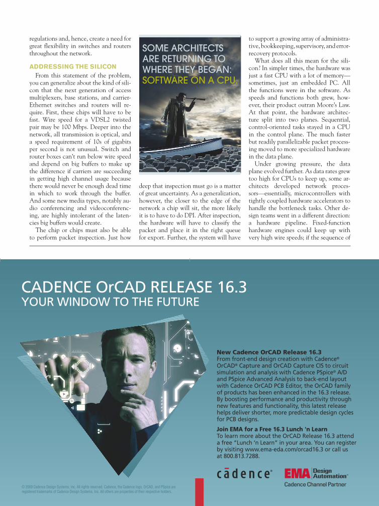
SOME ARCHITECTSARE RETURNING TOWHERE THEY BEGAN:SOFTWARE ON A CPU.
© 2009 Cadence Design Systems, Inc. All rights reserved. Cadence, the Cadence logo, OrCAD, and PSpice areregistered trademarks of Cadence Design Systems, Inc. All others are properties of their respective holders.
CadenceChannelPartner
CADENCE OrCAD RELEASE 16.3YOURWINDOW TO THE FUTURE
New Cadence OrCAD Release 16.3From front-end design creation with Cadence®
OrCAD® Capture and OrCAD Capture CIS to circuitsimulation and analysis with Cadence PSpice® A/Dand PSpice Advanced Analysis to back-end layoutwith Cadence OrCAD PCB Editor, the OrCAD familyof products has been enhanced in the 16.3 release.By boosting performance and productivity throughnew features and functionality, this latest releasehelps deliver shorter, more predictable design cyclesfor PCB designs.
Join EMA for a Free 16.3 Lunch 'n LearnTo learn more about the OrCAD Release 16.3 attenda free “Lunch ‘n Learn” in your area. You can registerby visiting www.ema-eda.com/orcad16.3 or call usat 800.813.7288.
edn091102df_id 22edn091102df_id 22 11/11/2009 2:38:48 PM11/11/2009 2:38:48 PM

tasks in packet processing remained thesame, simple data flows between pipe-line stages eliminated many of the loadsand stores inherent in a CPU-centric ar-chitecture, saving time and power.
But as protocols grew more diverseand complex, the fixed functions andfixed topologies broke down. Pipelinestages began to look like programmableaccelerators. “Life is too risky now forfixed-function pipelines,” says Xeler-ated’s Eklund. “Programmability is notnecessary only in the access fabric. It hasto go much deeper into the network.”Pipelines also sprouted thickets of con-ditional bypass and feedback paths and,eventually, accelerators of their own un-til the pipeline became just the centralengine in a network of processing ele-ments (Figure 1).
THE EVOLVING ENGINEThis growing complexity is erasing
the distinction between the control andthe data planes. At the same time, pro-cess migration is yielding less increasein circuit speed. As a result, some archi-tects are returning to where they began:software on a CPU. This time, though,the CPU is a multicore cluster with bothgeneral-purpose processors and specificaccelerators. Toby Foster, senior prod-uct marketing manager at Freescale, de-scribes such a device (Figure 2). “TheQorIQ chip family employs multiplee500 Power Architecture cores to coverapplications from line cards to base sta-tions and infrastructure,” he says. “As thecontrol and data planes merge, we seemulticore chips with datapath accelera-tors—a queue manager, a crypto engine,a regular-expression matcher—encroach-ing on the traditional ASIC approach.”
With all these cores, the traditionalbus-based interconnect structure is fail-ing, as well. To get the bandwidth thechip needs, architects provide each pro-cessing site, including the accelerators,with local caches, and they may tieevery thing together through a non-blocking switch fabric. If architects thenprovide hardware coherency across thecaches and fabric, the programmingmodel for the chip can approximatecoding for a single CPU.
Even with good cache design, how-ever, scheduling data movement undersoftware control in such a chip involvesa lot of work. “Traffic management ina multicore chip creates access issues,”
warns Satish Sathi, senior principal en-gineer at Applied Micro. “And theseissues involve fairness, QOS, and con-flicts for resources. You can resolve themin software, but that [approach] createsoverhead.”
Applied Micro’s approach is hard-ware-based virtualization. In effect,Sathi explains, the control software setsup a route through the engines on thechip for each category of packets. Anetwork of queues and a hardware-ar-bitration engine then steer the packetsthrough the maze of engines, buses, andbridges (Figure 3). “The arbitration en-gine does dynamic arbitration based onactual end-to-end congestion on thechip,” Sathi says. “Each packet gets in-spected at the end of each task and rout-ed to its next stop.”
It’s not a coincidence that this scenar-io sounds remarkably like a network—with nodes, routers, heterogeneous inter-connect, and virtual channels. Increas-ingly, networking chip architectures areleaving behind the idea of a CPU corewith accelerators on a bus and the con-cept of a CPU controlling a data-planepipeline. Instead, the chips are becomingminiature models of the networks theywill serve: heterogeneous collections ofprocessing and routing sites, heteroge-neous interconnect, virtual connections,and hardware-supported explicit routingof packet streams. The ideal we are ap-proaching is the ability to define a vir-tual data-flow machine for each packetflow on an underlying fabric of program-mable engines. Therein may lie the fu-ture not only of networking ICs but alsoof the SOC (system on chip) itself.EDN
Applied Microwww.appliedmicro.com
Arcturus Networkswww.arcturusnetworks.com
Broadcomwww.broadcom.com
ContinuousComputingwww.ccpu.com
FreescaleSemiconductorwww.freescale.com
SolarflareCommunicationswww.solarflare.com
Verizonwww.verizon.com
Xeleratedwww.xelerated.com
F OR M OR E I N F OR MATI ON
World-TrustedData Acquisition
Simple, Secure, Wi-Fi DAQ
� Up to 50 kS/s/ch, 24-bit measurement resolution
� 128-bit AES data encryption� Starting at $699*
Multifunction USB DAQ
� Up to 1.25 MS/s, 16 bits� Starting at $159*
High-Performance PC DAQ
� Up to 4 MS/s/ch, 16 bits� PCI and PXI Express
options available� Starting at $429*
©2008 National Instruments. All rights reserved. National Instruments, NI,and ni.com are trademarks of National Instruments. Other product andcompany names listed are trademarks or trade names of their respectivecompanies. *Prices subject to change. 2008-9625-301-101-D
>> Find the right DAQdevice for your project at ni.com/daq
800 454 6119
You can reachExecutive EditorRon Wilson at1-510-744-1263 [email protected].
edn091102df_id.indd 23edn091102df_id.indd 23 11/11/2009 2:40:36 PM11/11/2009 2:40:36 PM

BY BRIAN DIPERT • SENIOR TECHNICAL EDITOR
edn091102cs_id.indd 24edn091102cs_id.indd 24 11/12/2009 9:44:06 AM11/12/2009 9:44:06 AM

� �� �NOVEMBER 26, 2009 | EDN 25
� �
�
Flash-memory-based solid-state drives have recentlystirred up the staid storage industry, and their ini-tial success stories foretell a potentially stellar future.Consider, for example, how rapidly they’ve takenover the formerly robust market for 1.8-in. hard-diskdrives. Also consider their significant influence onsmaller-form-factor hard-disk drives’ lackluster initialunveilings. A notable percentage of netbook, tablet,and other alternative mobile computers, especially
those running Linux operating-system variants, contain solid-state drivesinstead of hard-disk drives. Thin and light conventional notebook PCsrunning Windows and OS X are also well along the conversion path.
Enterprise-computing applications mightat first glance seem to be poor candidates forsolid-state technology, given its substantiallyhigher cost than the magnetic alternative atthe high capacities that this market segmentrequires. Yet, by virtue of its low energy con-sumption, increased reliability, and ultrafastread rates, the technology is making notableprogress in conquering the corporate world.Consider that, to maximize hard drives’ per-formance, IT departments have long format-ted only the platters’ fastest-access portion,wasting the rest of the drive and therebyblunting the argument that hard drives costless than their nonmagnetic counterparts.Consider, too, that a number of applications,including smartphones, PDAs (personaldigital assistants), digital still cameras, andvideo cameras, that might have formerly gonewith—and, in some cases, in initial productgenerations, did go with—hard drives havemigrated en masse to solid-state storage.
Proponents of both approaches dispute theextent of solid-state technology’s potential toobsolete its predecessor, and the industry hasyet to determine a winner. These debates il-lustrate a number of fundamental misrepre-sentations of solid-state drives’ strengths andshortcomings. EDN readers’ feedback to pasteditorial coverage reveals similar misunder-standing (Reference 1). This article attemptsto clear up at least some of that confusion.
Cost, power consumption, and any otherall-important comparative factors aside, thedifferences between hard-disk and solid-statedrives boil down to a few fundamental points.First, solid-state drives, especially those inapplications with random-access patterns,read data substantially faster than hard drivescan, assuming the absence of any storage-to-system-interface bottlenecks. In contrast,solid-state drives, especially those in applica-tions with random-access patterns, write datamuch slower than hard drives do. Also, oncethe solid-state drive has depleted its inven-tory of spare capacity, block-erase delays be-come a larger percentage of the total write la-tency. Further, unlike with a hard-disk drive,flash memory is not fully bit-alterable. Al-though flash memory can change ones to ze-ros on a bit-by-bit basis, converting even asingle zero back into a one requires erasingthe entire block containing the bit.
Another difference is that flash memoryeventually “wears out” after extended erasecycles. However, it tends to do so on a block-by-block basis and in a predictable mannerthat the media controller can easily detectfar in advance and compensate for in a va-riety of ways. Many hard-drive failures, incontrast, are abrupt and systemic. Further,because solid-state drives are semiconductor-based, they are notably more immune to theeffects of abrupt shock, sustained vibration,
TO SERIOUSLY COMPETE WITH HARD-DRIVE MAKERS, SEMICONDUCTORVENDORS MUST AMASS A ROBUST, SUSTAINED SUPPLY OF SILICON FOR
SOLID-STATE DRIVES. THEY ALSO MUST ADDRESS PLENTY OF MISCONCEP-TIONS ABOUT THE NEWER TECHNOLOGY’S CAPABILITIES AND LIMITATIONS.
edn091102cs_id.indd 25edn091102cs_id.indd 25 11/12/2009 9:44:15 AM11/12/2009 9:44:15 AM

and other types of jarring. They’re alsocomparatively impervious to environ-mental interference, such as from mag-netic fields.
Most of today’s flash memory uses aconceptually common floating-gate cellstructure (Figure 1). Fast-random-read-access NOR and slower—albeit less ex-pensive on a per-bit basis—NAND tech-nologies differ predominantly in theircell-to-cell interconnect schemes. In itsdefault erased state, the transistor turnson—that is, outputs a one—when thememory device’s integrated address-de-coding circuitry activates the necessary
array row and column lines to selectit. With the transistor programmed bymeans of additional electrons stored onits floating gate, it cannot turn on whenaddress inputs select it and therefore out-puts a zero to read attempts.
Altering the stored value of a flash-memory transistor involves the appli-cation of higher-than-normal voltagesto various transistor junctions, there-by creating the necessary electric fieldsto affect electron flow onto or off thefloating gate. Initial flash-memory gen-erations required off-chip generation ofthese voltages; nowadays, most devicesemploy on-die high-voltage pumps forthis function. Theoretically, you couldalter a transistor’s value—both for one-to-zero programming and for zero-to-one erasure—on a bit-by-bit basis, as isthe case with EEPROMs (electricallyerasable programmable read-only mem-ories), FRAMs (ferroelectric random-access memories), MRAMs (magneticRAMs), and battery-backed SRAMs(static RAMs). The necessary signal-routing, isolation, and other circuitry,
however, would use too much die areaand would therefore be too expensive atthe IC capacities that bulk-storage appli-cations require.
With modern NAND flash memory,on the other hand, you can erase blocksin approximately 512-kbyte increments.Bit-by-bit programming is possible; froman efficiency standpoint, however, solid-state drives and the NAND chips with-in them prefer to write data in approxi-mately 4-kbyte chunks. This preferencereflects the cost-versus-performance sizesof the RAM buffers on the flash-memo-ry die. The bulk-alteration requirementdifferentiates flash memory not onlyfrom other nonvolatile semiconductor-
SOURCELINE
BITLINE
P
WORD-LINECONTROL GATE
FLOATING GATE
NN
26 EDN | NOVEMBER 26, 2009
Figure 1 Most single-transistor flash-memory cells operate in a conceptually similar fashion (a) regardless of whether they intercon-nect in a NOR (b) or a NAND (c) scheme. Bit-by-bit or more efficient page-by-page programming places incremental charge on thefloating gate (d), thereby counteracting an applied turn-on voltage during subsequent reads. Block-by-block erasure (e) removes thischarge surplus (courtesy the Wikipedia Foundation).
WORDLINE 0
WORDLINE 1
WORDLINE 2
WORDLINE 3
WORDLINE 4
WORDLINE 5
BIT LINE
N N GND N N GND N NN GND
P
GROUND-SELECTTRAN-
SISTOR
BIT-LINE-SELECTTRAN-
SISTOR
BIT LINE
WORDLINE 0
WORDLINE 1
WORDLINE 2
WORDLINE 3
WORDLINE 4
WORDLINE 5
WORDLINE 6
WORDLINE 7
N N N N N N N N N N N
P
12V
0V
FLOATINGGATE
DRAINSOURCE12V
200A
FLOATINGGATE
DRAINSOURCE
200A
0V
OPEN
12V
FROM ANEFFICIENCYSTANDPOINT, SOLID-STATE DRIVES ANDTHE NAND CHIPSWITHIN THEM PREFERTO WRITE DATA INAPPROXIMATELY4-KBYTE CHUNKS.
(a)
(d)
(e)
(b)
(c)
edn091102cs_id.indd 26edn091102cs_id.indd 26 11/12/2009 9:44:26 AM11/12/2009 9:44:26 AM

NOVEMBER 26, 2009 | EDN 27
storage technologies but also from hard-disk drives. The repeated electron flowacross the thin silicon layer between theflash-memory transistor’s substrate andfloating gate and through incrementalprogram and erase cycles stresses the ox-ide. At first, electrons inadvertently be-come trapped in the oxide lattice, im-peding the flow of other electrons andslowing subsequent program and eraseoperations. Eventually, the oxide breaksdown by rupturing, for example, leadingto fundamental transistor failure. Thisdemise tends to disrupt the function ofthe entire erase block that contains theaffected transistor.
Modern flash memories come inboth SLC (single-level-cell) and MLC(multi level-cell) variants; today’s MLCvariants are primarily 2-bit-per-cell de-vices (Figure 2). With SLC flash mem-ories, the voltage-sensing circuitry thatconnects to the array transistors’ out-puts can be relatively simple becauseit needs to discern only one voltagethreshold and because the transistor’sone and zero output voltages have sub-stantial margin to this threshold. How-ever, with a 2-bit-per-cell MLC flashmemory, three voltage thresholds—thatis, four levels—require discernmentduring reads. The programming opera-tion for placing the necessary amountof electron charge onto the transistor’sfloating gate is similarly precise, and theeffects of supply-voltage and operating-temperature variation and cycling fur-ther complicate this operation. Span-
sion claims that its MirrorBit MLCtechnology approach somewhat reduc-es the need for precise electron place-ment. Nonetheless, the concept re-mains largely relevant.
It’s probably no surprise that MLCreads and writes—that is, programs—are substantially slower than their SLC
counterparts and that the maximumblock-cycling specifications for MLCmemories are on average an order ofmagnitude less than those of SLC chips.These fundamental trade-offs are neces-sary for obtaining a lower per-bit cost forMLC storage devices (Table 1).
Now, consider Intel and Micron Tech-nology’s new 3-bit-per-cell memoriesand that Sandisk recently began produc-ing 4-bit-per-cell X4 devices (Reference2). The difference between any two se-quential voltage levels and, hence, de-coded-bit combinations with these newdevices is on the order of 100 or so elec-trons or fewer in some cases. This situa-tion represents a profound challenge forsemiconductor-process and -product en-gineers. By potentially hampering bothperformance and data dependability, itcalls into question the chips’ suitabilityfor applications requiring highly reliablestorage. Then again, folks not too longago were saying the same thing about 2-bit-per-cell MLC flash memory.
CONTROLLER CHOICESThe media controller may be a hard-
ware-centric device, a software-fueledCPU, or any combination thereof. Thehardware-versus-software choice of acontroller involves trading off cost, per-formance, and power consumption ver-sus flexibility and the ability to upgrade.Whatever its composition, the mediacontroller acts as a bridge between theflash memories and the conventionalhardware and software interfaces thatthe CPU, core-logic chip set, and othersubsystems expect. The controller alsomanages the data stored in the single-component or multicomponent mergedflash-memory array to avoid “hot-spot”overcycling of any erase blocks in thearray, ideally as a background functionthat is invisible to the host both in ac-cess time and in any other regard. Thecontroller leverages flash memory’sstrengths and mitigates its read- andwrite-speed weaknesses. The result is,with any luck, at least on par with—and, ideally, much faster than—thehard-drive alternative.
One perhaps obvious way of boostingeffective solid-state-drive performanceat the expense of incurring higher powerconsumption is to access multiple com-ponents in parallel using several ad-dress-, data-, and control-line channels
AT A G LAN CE� Solid-state storage offers manybenefits over the currently dominantrotating magnetic alternative, butkey differences require consider-ation and accommodation.
� Operating systems and theirunderlying file systems makeassumptions about mass storage’slong-latency random accesses andfull bit alterability. Neither assump-tion is valid in the flash-memory era.
� Both operating systems’ andsystem firmware’s full support for anew ATA (advanced-technology-attachment) command promises tosubstantially simplify the flash-mediacontroller’s task, thereby boostingwrite performance.
� Operating systems can make keycustomizations to their functionsonce they know that they’re talkingto a solid-state drive instead of ahard-disk drive.
� Hardware evolutions, by discard-ing vestigial interfaces and extrane-ous functions, can notably optimizesystems’ solid-state driveimplementations.
DISTRIBUTION OF CELLS
1 0
VT
REFERENCE POINT
DISTRIBUTION OF CELLS
VT
REFERENCE POINTS
11 10 01 00
Figure 2 Whereas conventional 1-bit-per-cell flash memory has plenty of margin withinthe threshold-voltage envelope between a sensed zero and a sensed one (a), 2-, 3-,and 4-bit-per-cell technologies are more challenging to reliably implement across sup-ply-voltage, temperature, and erase-cycling ranges (b) (courtesy Micron Technology).
(a)
(b)
edn091102cs_id.indd 27edn091102cs_id.indd 27 11/12/2009 9:44:28 AM11/12/2009 9:44:28 AM

between the controller and the flashmemories. You can then not only simul-taneously read, program, or erase multi-ple array elements, but also juggle mul-tiple operations with different ICs. Forexample, you could read from one whilewriting or erasing another if the system’saccess profiles justify this added levelof controller complexity. In choosing amultichannel scheme, however, you al-so multiply the granularity of the solid-state drive’s capacity and the effectivesizes of program pages and erase blocks.This situation might warrant the choiceof a flexible controller design that canrun in either single-channel or multi-channel mode.
Modern flash memories exhibit sig-nificant disparities between program-page and erase-block sizes and betweenprogram and erase times. The controllershould, therefore, manage the media insuch a way that background-erase opera-tions for wear-leveling purposes—whichmanufacturers also commonly call house-keeping, garbage collection, and merg-ing—on a component or a block withinthat component don’t collide with sys-
tem-write-request-initiatedforeground
programming operations on that samecomponent or block or, for that matter,foreground system-read requests. Em-bedding a large RAM cache on the sol-id-state drive, much like the buffers onmodern hard drives, can also be an effec-tive collaborator to system-side buffer-ing in mitigating any perceived decreasein performance that these housekeep-ing tasks incur. The trade-off of this ap-proach, however, is that it requires moreparts.
Reads and writes were traditionally theonly required storage functions because,unlike with flash memory, you couldfully overwrite hard-drive media on abit-by-bit basis. A file-deletion requestcauses the file system to update its inter-nal tables accordingly, but it historicallydidn’t pass that information to the drive.Hence, the solid-state-drive controlleris unaware that it can do backgroundcleanup to free up the relevant pages andblocks containing them for future writes.The necessary erase and program opera-tions occur only after the file system re-quests an explicit overwrite of the LBAs(logical-block addresses) associated withthe drive’s now-invalid PBAs (physical-block addresses). These operations arethen unfortunately in the foreground
where they adversely affect perceivedread and write speed.
Manufacturers typi-cally ship solid-
state drivesf r om
the factory with spare “fresh” capac-ity, which is invisible to the operatingsystem. The controller uses this capac-ity to delay the inevitable onset of thenoted performance-strapping scenarios.However, good news is on the way inthe form of the “trim” command, whichthe T13 Technical Committee of theINCITS (International Committee forInformation Technology Standards) isnow standardizing as part of the ATA(advanced-technology-attachment)command set. At press time, the T10Technical Committee had not yet re-vealed its plans for the SCSI (small-computer-system-interface) commandset. Before a system uses the trim com-mand, it interrogates the drive to de-termine rotation speed. If it encountersa 0-rpm response, the system assumesthat it is dealing with a solid-state diskand does further queries to determinewhether trim support exists along withother relevant parameters. The trimcommand informs the drive that pagesstored within the array are no longervalid and are therefore candidates forhousekeeping. Deletion of a file withina trim-cognizant operating system re-sults in the sending of relevant informa-tion for the corresponding LBAs to thedrive’s controller.
Although the trim command candramatically improve sustained solid-state-drive performance in applicationsrequiring many file deletions, it’s in-effective in cases in which file updates
TABLE 1 REPRESENTATIVE 1- AND 2-BIT-PER-CELL NAND-FLASH-MEMORY SPECIFICATIONS
TechnologyErase specifi cation
(cycles)
Program-pagesize
(kbytes)
Erase-blocksize
(kbytes)
Random-readlatency(�sec)
Per-pageprogram time
(kbytes)
Per-blockerase time
(msec)
SLC (1-bit-per-cell) fl ash memory
100,000 4 512 25 250 2
MLC (2-bit-per-cell) fl ash memory
10,000 4 512 50 900 2
Figure 3 Most of today’ssolid-state drives, such as
Intel’s X25 units, use conven-tional storage interfaces andwill benefit from those interfaces’
evolutionary performance improve-ments (a). More revolutionaryapproaches migrate to alterna-tive system interfaces withcloser proximity to the CPU,such as Fusion-io’s approach
with PCIe (b) and Spansion’sapproach with DRAM (c).
(a)
(b)
(c)
28 EDN | NOVEMBER 26, 2009
edn091102cs_id.indd 28edn091102cs_id.indd 28 11/12/2009 9:44:29 AM11/12/2009 9:44:29 AM

occur, such as when you open a docu-ment for editing and then save the up-dated version or with Microsoft Out-look’s PST database format. More gen-erally, it exposes the weakness inherentin the strong linkage between LBAsand PBAs in FFSs (flash file systems).Sandisk’s venerable FFS, along with theFTL (flash-translation-layer) technol-ogy the company obtained when it ac-quired M-Systems in mid-2006, strivesto provide PBA independence for fre-quently updated files, such as the Win-dows Registry and the FAT (file-alloca-tion table).
The company unveiled its Ex-tremeFFS at January’s CES (ConsumerElectronics Show) and both implementsit in its products and makes it availablefor licensing. ExtremeFFS further seversexplicit LBA-to-PBA linkage, therebyclaiming to boost random write speedsby a factor as great as 100 times. Ex-tremeFFS makes less efficient use of theflash-memory media to accomplish thisobjective; Sandisk declines to providespecifics. Given the burgeoning capaci-ties available with lithographies such asIntel and Micron’s latest 34-nm process,
however, the incremental ExtremeFFSoverhead will over time become less ofa practical issue.
SYSTEM OPTIMIZATIONSSolid-state units are currently shoe-
horning themselves into legacy hard-drive designs to leverage that technol-ogy’s huge market, thereby jump-start-ing the solid-state-storage ramp-up(Figure 3). But as solid-state drives be-come more prevalent and presumably,therefore, a from-the-start implementa-tion choice, a carefully crafted software/hardware implementation can optimallybenefit from flash memory’s unique ca-
pabilities. Consider, for example, com-mon file-system operations, such as pe-riodic automatic disk defragmentation,prefetching, file-location optimization,and system-side caching. These featuresall aim to compensate for hard drives’head-relocation and platter-rotation la-tencies, which cause slow random readaccesses. Neither of these latencies is afactor with solid-state drives. Eliminat-ing such workarounds can consequentlyimprove system cost, power consump-tion, and other key variables and can re-duce flash-media cycling.
Microsoft’s latest Windows 7 oper-ating system makes such adjustmentswhen it detects a solid-state drive’s pres-ence in a system using the same schemeit uses for assessing trim support (Refer-ence 2). Trim cognizance extends be-yond simple file-deletion operations toencompass the full range of related func-tions, such as partition formats and sys-tem snapshots. Avoiding random-loca-tion writes whenever possible to boostperformance can benefit both hard-disk- and solid-state-drive technologies.Integrated file-compression support forflash-memory-housed data can reduce
A CAREFULLYCRAFTED SOFT-WARE/HARDWAREIMPLE MENTATIONCAN OPTIMALLYBENEFIT FROM FLASHMEM ORY’S UNIQUECAPABILITIES.
High Performance� Up to 60 dB CM attenuation
� Up to 80 dB DM attenuation
� Up to 14 A and 80 V
� Supports EN55022, Class B limits
Very Small Size� <50% area vs. most passive filters
� Low profile (4.5 mm) SMT package
� Optional Integrated Hot-Swapfor even greater space savings
Typical DC-DC Converter Input EMI
DC- DC EMI NOISE ...CANCELLATIONPicor QUIETPOWER™ Active Filters suppress EMI AND save PCB space
picorpower.com/QPI/edn • 800-735-6200
AVAILABLE!Easy to Use
Evaluation Boards Call 800-735-6200
ONLY 1 in2
QUIETPOWER™
Defining the Quality of Power through Innovation
edn091102cs_id 29edn091102cs_id 29 11/12/2009 10:25:08 AM11/12/2009 10:25:08 AM
the per-bit cost gap between the tech-nologies. Windows 7 and its peers alsoare more scrupulous about, for example,ensuring that partition- and file-loca-tion endpoints align with—rather thanoverlap—flash memory’s write-pageboundaries. And solid-state drives mayprovide an opportunity to reduce thesystem DRAM’s budget requirement toless than it was in the hard-drive-centricpast, thanks to solid-state’s fast-access—at least for reads—virtual-memory-pag-ing scheme.
System-hardware interfaces provideanother opportunity for optimization.Except perhaps with extremely high-ro-tations-per-minute, enterprise-tailoredunits, hard drives tap the bandwidthcapability of modern storage interfac-es, such as 3-Gbps SATA (serial ATA)and SAS (serial attached SCSI), onlywhen doing transfers to and from thedrive’s RAM buffer. Solid-state drivesconversely can make more meaning-ful use of the performance potential ofSATA and SAS, and the two technolo-gies’ performance gap will only increasein the upcoming 6-Gbps serial-storage-interface generation (references 3 and
4). Similar disparities are likely withthe upcoming 4.8-Gbps USB (Univer-sal Serial Bus) Version 3 and with Intel’sembryonic Light Peak optical-interfacetechnology.
But why restrict yourself to a legacystorage interface at all? Companies suchas Fusion-io have figured out that PCIe(Peripheral Component InterconnectExpress)-based add-in cards can boostperformance by moving the solid-statedrive closer to the CPU with which it’sinteracting. Giving the flash memory,either on a module or directly attachedto the system board, a dedicated inter-face to the chip set affords an even closerlinkage. Intel uses this approach with itsTurbo memory cache, for example. Theapproach incurs a trade-off, however,in that it makes it more difficult for theend user to later alter the system-mem-ory allocation. Alternatively, you canuse the DRAM bus, as Intel’s 28F016XDflash memory attempted to do in themid-1990s and as Spansion’s EcoRAMdoes today. In such a configuration, youmight even be able to dispense with adedicated flash-memory-controller chip,instead employing software running on
the host CPU or circuitry within thechip set’s logic.EDN
R E FE R E N CE S1 Dipert, Brian, “Solid-state drives chal-lenge hard disks,” EDN, Nov 13, 2008,pg 25, www.edn.com/article/CA6611643.2 “Engineering Windows 7,” MicrosoftCorp, 2009, http://blogs.msdn.com/e7/archive/2009/05/05/support-and-q-a-for-solid-state-drives-and.aspx.3 Dipert, Brian, “Speedy simplicity:serial-storage interfaces,” EDN, Jan 22,2004, pg 33, www.edn.com/article/CA373882.4 Dipert, Brian: “Interface overkill? IseSATA necessary for your next systemdesign?” EDN, May 10, 2007, pg 48,www.edn.com/article/CA6437950.
You can reach
Senior Technical Editor
Brian Dipert
at 1-916-760-0159,
and www.bdipert.com.
© 2009 Cadence Design Systems, Inc. All rights reserved. Cadence, the Cadence logo, OrCAD, and PSpice areregistered trademarks of Cadence Design Systems, Inc. All others are properties of their respective holders.
CadenceChannelPartner
CADENCE OrCAD RELEASE 16.3YOURWINDOW TO THE FUTURE
New Cadence OrCAD Release 16.3From front-end design creation with Cadence®
OrCAD® Capture and OrCAD Capture CIS to circuitsimulation and analysis with Cadence PSpice® A/Dand PSpice Advanced Analysis to back-end layoutwith Cadence OrCAD PCB Editor, the OrCAD familyof products has been enhanced in the 16.3 release.By boosting performance and productivity throughnew features and functionality, this latest releasehelps deliver shorter, more predictable design cyclesfor PCB designs.
Join EMA for a Free 16.3 Lunch 'n LearnTo learn more about the OrCAD Release 16.3 attenda free “Lunch ‘n Learn” in your area. You can registerby visiting www.ema-eda.com/orcad16.3 or call usat 800.813.7288.
edn091102cs_id 30edn091102cs_id 30 11/12/2009 10:36:30 AM11/12/2009 10:36:30 AM

Audio TransformersImpedance Levels 10 ohms to 250k ohms,Power Levels to 3 Watts, Frequency Response±3db 20Hz to 250kHz. All units manufacturedand tested to MIL-PRF-27. QPL Unitsavailable.
Power & EMIInductorsIdeal for noise, spike and Power FilteringApplications in Power Supplies, DC-DCConverters and Switching Regulators
Pulse Transformers10 Nanoseconds to 100 Microseconds. ETRating to 150 Volt Microsecond, Manufacturedand tested to MIL-PRF-21038.
Multiplex Data BusPulse TransformersPlug-In units meet the requirementsof QPL-MIL-PRF 21038/27Surface units are electrical equivilentsof QPL-MIL-PRF 21038/27.
DC-DC ConverterTransformersInput voltages of 5V, 12V, 24V And 48V.Standard Output Voltages to 300V (Specialvoltages can be supplied). Can be used as selfsaturating or linear switching applications. Allunits manufactured and tested to MIL-PRF-27.
400Hz/800HzPowerTransformers0.4 Watts to 150 Watts. Secondary Voltages 5Vto 300V. Units manufactured to MIL-PRF-27Grade 5, Class S (Class V, 1550C available).
DELIVERY-stock to one week
for sample quantities
Electronics, Inc.143 Sparks Ave. Pelham, NY 10803 • Call Toll Free 800-431-1064 • fax: 914-738-8225
See PICO’s full Catalog Immediately on the internet
www.picoelectronics.comE-mail: [email protected]
PICO Transformersand Inductors
Over 5000 Standard
From .19” ht.
Send for free 180 pg PICO Catalog
(and Plug-In)Surface Mount
edn091102.indd 31edn091102.indd 31 11/5/2009 1:51:18 PM11/5/2009 1:51:18 PM

edn091102 32edn091102 32 11/11/2009 10:19:48 AM11/11/2009 10:19:48 AM
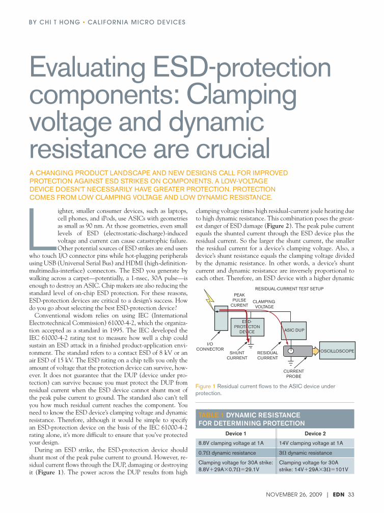
Lighter, smaller consumer devices, such as laptops,cell phones, and iPods, use ASICs with geometriesas small as 90 nm. At those geometries, even smalllevels of ESD (electrostatic-discharge)-inducedvolt age and current can cause catastrophic failure.Other potential sources of ESD strikes are end users
who touch I/O connector pins while hot-plugging peripheralsusing USB (Universal Serial Bus) and HDMI (high-definition-multimedia-interface) connectors. The ESD you generate bywalking across a carpet—potentially, a 1-nsec, 30A pulse—isenough to destroy an ASIC. Chip makers are also reducing thestandard level of on-chip ESD protection. For these reasons,ESD-protection devices are critical to a design’s success. Howdo you go about selecting the best ESD-protection device?
Conventional wisdom relies on using IEC (InternationalElectrotechnical Commission) 61000-4-2, which the organiza-tion accepted as a standard in 1995. The IEC developed theIEC 61000-4-2 rating test to measure how well a chip couldsustain an ESD attack in a finished product-application envi-ronment. The standard refers to a contact ESD of 8 kV or anair ESD of 15 kV. The ESD rating on a chip tells you only theamount of voltage that the protection device can survive, how-ever. It does not guarantee that the DUP (device under pro-tection) can survive because you must protect the DUP fromresidual current when the ESD device cannot shunt most ofthe peak pulse current to ground. The standard also can’t tellyou how much residual current reaches the component. Youneed to know the ESD device’s clamping voltage and dynamicresistance. Therefore, although it would be simple to specifyan ESD-protection device on the basis of the IEC 61000-4-2rating alone, it’s more difficult to ensure that you’ve protectedyour design.
During an ESD strike, the ESD-protection device shouldshunt most of the peak pulse current to ground. However, re-sidual current flows through the DUP, damaging or destroyingit (Figure 1). The power across the DUP results from high
clamping voltage times high residual-current joule heating dueto high dynamic resistance. This combination poses the great-est danger of ESD damage (Figure 2). The peak pulse currentequals the shunted current through the ESD device plus theresidual current. So the larger the shunt current, the smallerthe residual current for a device’s clamping voltage. Also, adevice’s shunt resistance equals the clamping voltage dividedby the dynamic resistance. In other words, a device’s shuntcurrent and dynamic resistance are inversely proportional toeach other. Therefore, an ESD device with a higher dynamic
BY CHI T HONG • CALIFORNIA MICRO DEVICES
Evaluating ESD-protectioncomponents: Clampingvoltage and dynamicresistance are crucialA CHANGING PRODUCT LANDSCAPE AND NEW DESIGNS CALL FOR IMPROVEDPROTECTION AGAINST ESD STRIKES ON COMPONENTS. A LOW-VOLTAGEDEVICE DOESN’T NECESSARILY HAVE GREATER PROTECTION. PROTECTIONCOMES FROM LOW CLAMPING VOLTAGE AND LOW DYNAMIC RESISTANCE.
RESIDUAL-CURRENT TEST SETUP
ASIC DUP
OSCILLOSCOPE
CURRENTPROBE
I/OCONNECTOR
RESIDUALCURRENT
SHUNTCURRENT
CLAMPINGVOLTAGE
ESD-PROTECTON
DEVICE
ESD-PROTECTON
DEVICE
PEAKPULSE
CURENT
Figure 1 Residual current flows to the ASIC device underprotection.
NOVEMBER 26, 2009 | EDN 33
TABLE 1 DYNAMIC RESISTANCEFOR DETERMINING PROTECTION
Device 1 Device 2
8.8V clamping voltage at 1A 14V clamping voltage at 1A
0.7� dynamic resistance 3� dynamic resistance
Clamping voltage for 30A strike:8.8V�29A�0.7��29.1V
Clamping voltage for 30Astrike: 14V�29A�3��101V
edn091102ms4335_id 33edn091102ms4335_id 33 11/11/2009 10:37:49 AM11/11/2009 10:37:49 AM

resistance allows more residualcurrent to flow to the DUP.
Dynamic resistance and clamp-ing voltage determine how well anESD-protection device protectsagainst residual current. Duringroutine operations, the protec-tion device must maintain a highimpedance. However, when anESD strike hits, the protectiondevice rapidly shunts ESD energyto ground. Data sheets may list dy-namic resistance. If the data sheetyou are looking at doesn’t list thisspec, however, you can calculateit from a graph of the device’sclamping voltage versus peakpulse current for IEC 61000-4-2Level 4, in which the peak pulsecurrent is 30A. Clamping voltagematters more than operating volt-age when comparing protectiondevices. During an ESD strike, anESD device’s lower clamping volt-age minimizes ESD damage dueto joule heating. So both a lowclamping voltage and low dynamicresistance provide a more accuratemetric of how an ESD device willwork during a strike (Figure 3).
Because dynamic resistance isthe yardstick by which you shouldmeasure protection devices, thequestion is how to calculate thisparameter if the data sheet doesnot list it. You can easily calcu-late dynamic resistance as a slopeon a graph of clamping voltageversus peak pulse current, with apeak pulse current of 0, 1, 2, and3A and so on. After 1A, the slopeof dynamic resistance is close tolinear. You can also calculate thisparameter from clamp-voltagenum bers with corresponding peakpulse current because a device’sdynamic resistance is the slopeof the graph equal to one clamp-ing voltage minus another clamp-ing voltage divided by the peakpulse current minus another peakpulse current. The formula for de-termining clamping voltage at apeak pulse current of 30A for IEC61000-4-2 is to add the breakdownvoltage to the peak pulse currentand multiply that result by the dy-namic resistance.
34 EDN | NOVEMBER 26, 2009
Figure 2 Catastrophic failure of the DUP may occur when the ESD device’s dynamic resis-tance is high.
Figure 3 High dynamic resistance increases residual current to the DUP. Low dynamic resis-tance decreases residual current to the device under protection. A protection device offeringlow dynamic resistance makes a path for an ESD strike and shunts current away from thedevice under protection, thereby minimizing residual current to the DUP.
TABLE 2 ESD-DIODE-PROTECTION DEVICE VERSUS SUPPRESSOR/VARISTOR PERFORMANCEVoltage
(kV) ESD diodeDevice under
protectionPeak clampvoltage (V)
Residualcurrent (A)
Residual peakmaximum/total (VA)
4 Pass Pass 47.97 4.68 152.02
6 Pass Pass 68.23 6.83 351.66
12 Pass Pass 137.33 14.43 1787.4
Voltage(kV)
Suppressor/varistor
Device underprotection
Peak clampvoltage (V)
Residualcurrent (A)
Residual peakmaximum/total (VA)
4 Pass Pass 162.33 14.78 1405.65
6 Pass Fail 181.77 16.24 2253.56
edn091102ms4335_id 34edn091102ms4335_id 34 11/11/2009 10:37:50 AM11/11/2009 10:37:50 AM

The residual current flowing througha “protected” chip is proportional tothe dynamic resistance of the protec-tion device versus the resistance in therest of the circuit. Dynamic resistance isthe most important factorin determining protectionfrom ESD. All other thingsbeing equal, a 5V ESDdiode is only marginallybetter than a 3.3V diode(Table 1). When compar-ing devices, bear in mindthe dynamic resistance, which affectsthe residual current, rather than thebreakdown voltage.
ESD diodes and suppressor/varistorshave different performance. Table 2shows the specs of a system that sur-vived a 12-kV strike using a diode-pro-tection device but failed at 6 kV usinga high-dynamic-resistance suppressor.Note that the varistor survived, but thesystem failed. Note also that both theclamping voltage and the residual cur-rent are much higher with varistors.
The availability of two-stage ESD-pro-tection architectures means engineersneed not choose between signal integ-rity and ESD protection. A two-stageESD architecture offers more protectionfor a DUP when a single-stage ESD ar-chitecture is insufficient for providinglower dynamic resistance and therefore
higher residual current. The first stageacts as a traditional ESD device, low-ering clamping voltage and dynamicresistance, and the second stage furtherreduces clamping vol tage and residual
current (Figure 4).The fact that a device
has low clamping volt-age doesn’t mean that itoffers higher protection.When creating your de-sign, therefore, the mostimportant parameters for
comparison between ESD-protectiondevices are clamping voltage, dynamicrange, and the total number of protectionstages in the device. These parameters letyou know before you specify an ESD de-vice whether that device is right for yourapplication.EDN
AUTH OR’S B I OG RAPHYChi T Hong is a senior application engineerat California Micro Devices (Milpitas,CA). He received bachelor’s and master’sdegrees from the University of SouthernCalifornia (Los Angeles). For more infor-mation on two-stage ESD devices, go to theXtremeESD products page at www.cmd.com.
ACK N OWLE D G M E NTThanks go to Allen Tung of CaliforniaMicro Devices for his help with this article.
Figure 4 A two-stage ESD-protection architecture provides dual-stage clamping to limitboth clamping voltage and residual current from reaching the DUP.
Go to www.edn.com/ms4335 and clickon Feedback Loop topost a comment onthis article.
+
NOVEMBER 26, 2009 | EDN 35
U L T R A M I N I A T U R E
Surface MountAudio
Transformers
• Manufactured and testedto MIL-PRF-27
• Frequency range20 Hz to 250 KHz
• Available from100 milliwatts to 3 watts
• Impedance from 20 ohmsto 100 K ohms
• Operating temperature-550C to +130oC
• Low Profile from .24"ht.• Thru-Hole available
See EEMor send direct
for FREE PICO CatalogCall toll free 800-431-1064
in NY call 914-738-1400Fax 914-738-8225PICO Electronics,Inc.
143 Sparks Ave.. Pelham, N.Y. 10803E Mail: [email protected]
Delivery-Stock to one weekfor sample quantities
See full Catalog immediately
www.picoelectronics.com
Low Profile from
.24"ht.
edn091102ms4335_id.indd 35edn091102ms4335_id.indd 35 11/11/2009 2:35:17 PM11/11/2009 2:35:17 PM

The application of electromagnetics has been inpractice for more than a century: In 1831, Englishchemist and physicist Michael Faraday invent-ed the transformer, although he called it an in-duction coil. Unfortunately, engineering schoolsrarely provide instruction in practical magnet-
ics relevant to SMPS (switch-mode-power-supply) applica-tions. Part of the problem is that the classic design equationsfor magnetics target sinusoidal waveforms, but SMPSs operatewith rectangular waveforms.
The starting point for understanding magnetics is to lookat the relationships between current flow and electric andmagnetic fields. Figure 1 shows a simple air-cored winding.A current-carrying conductor creates its own magnetic field(B), which produces flux lines around the conductor. In thisexample, 10 turns of wire carry a dc current, and each turncreates its own magnetic field. The fields combine to createa concentrated and fairly linear field within the winding; thefield diverges and weakens outside the winding. The magneticfield inside the winding is the primary storage area for energy,but the external field can also store a significant amount.
If you place an object comprising a magnetic material, suchas iron, within the winding, the magnetic field exerts an EMF(electromotive force) on the object. If you then place a secondwinding within the field and the primary winding is carrying accurrent so the field is changing with time, the magnetic fieldwill induce a current to flow within the second winding. Lenz’sLaw, which Russian chemist and physicist Heinrich Lenz pos-tulated in 1834, states that an induced current always flows in adirection opposing the motion or change causing it.
Thus, you can describe the properties of a magnetic field interms of its intensity or its density. The magnetic-field inten-sity defines the field’s ability—in ampere turns per meter—toexert forces on magnetic poles. The magnetic-flux density (B)is the ability of the magnetic field, in teslas, to induce an elec-tric field when it changes. This property introduces the di-mension of time.
Two laws—Ampere’s and Faraday’s—jointly govern the re-lationship between magnetic components and their character-istics you see from the terminals. Ampere’s Law, which Frenchphysicist and mathematician André-Marie Ampère postu-lated in 1826, relates the integrated magnetic field around aclosed loop to the electric current passing through the loop.
Faraday’s Law, which Faraday postulated in 1834, states thatthe induced EMF or EMF in any closed circuit equals the timerate of change of the magnetic flux through the circuit.
You may wonder why magnetic circuits require cores. An-swering this question requires consideration of another char-acteristic, permeability—a measure of the amount of flux amagnetic field can push through a unit volume of material.You would not expect the winding in Figure 1 to perform wellas an electromagnet because it has no core. However, if youinsert an iron core in the center of the windings, it can makea powerful electromagnet because the permeability of iron isabout 10,000 times that of free space, enabling the concentra-tion of a relatively large amount of magnetic flux between thewindings. Permeability is roughly analogous to conductivity inthe electrical realm. Table 1 shows the equivalence betweenthe magnetic and the electrical domains. Just as a conductoris a conduit for energy to flow in the form of an electrical cur-rent, a high-permeability magnetic material acts as a conduitfor energy to flow as magnetic flux.
It is important to account for leakage in magnetic circuits.Many parallels exist between the electrical and the magneticrealms. However, compared with free space, the conductivityof common conductors, such as copper, at approximately 1020,is much higher than the permeability of magnetic materials, atapproximately 104. Thus, you can easily ignore leakage currents,
BY SAMEER KELKAR • POWER INTEGRATIONS
What every designer shouldknow about magnetics inswitch-mode power suppliesPOWER IS OFTEN AN AFTERTHOUGHT IN SYSTEM DESIGN, BUT THE CHOICEAND DESIGN OF THE MAGNETIC ELEMENTS AT THE HEART OF AN SMPS ARECRUCIAL. ACQUAINT OR REACQUAINT YOURSELF WITH THE FUNDAMENTALSOF THIS FREQUENTLY OVERLOOKED AREA.
BB
I
I
ו
Figure 1 In a simple air-cored winding, a current-carrying con-ductor creates its own magnetic field, which produces flux linesaround the conductor (a); 10 turns of wire carry a dc current,and each turn creates its own magnetic field (b).
(a) (b)
36 EDN | NOVEMBER 26, 2009
edn091102ms4346_ID 36edn091102ms4346_ID 36 11/12/2009 9:46:45 AM11/12/2009 9:46:45 AM

but not leakage flux, in low-frequency systems. Although per-meability is analogous to conductivity, it is not a linear charac-teristic for many materials and takes a different value depend-ing on what previously occurred (Figure 2).
Figure 2a shows the relationship between magnetic-fieldintensity, H, and magnetic-flux density, B, in a ferromagnet-ic material. The slope of this curve at any given time is theinstantaneous permeability (�R) of the material. For low val-ues of intensity, permeability is constant and relatively high.However, for larger values of intensity, permeability starts de-creasing to the point that the material starts resembling freespace (�R=1). Thus, you need a larger and larger magnetic-field intensity to produce a small increase in the density field.At this point, the material reaches saturation.
The area between the rising BH curve and the vertical axisrepresents energy stored in the material. If you then reduce thefield intensity from the saturation point, you can recover en-ergy from the material; however, the energy you recover is lessthan that stored, so the BH curve follows a different path. Theresult for a complete cycle is that the BH curve forms a closed Sshape. The area the S encloses represents the hysteresis curve,or the total lost energy in the cycle. The area of the curve is afunction of the frequency; thus, at higher frequencies, the areaof the hysteresis curve increases, and so do the losses.
The total flux, or flux linkage, relates to the electrical cur-rent through the inductance constant. Thus,
LNIM ,=φ
where LM is the inductance constant, N� is the flux linkage,and I is the electrical current. Further,
A B B H HN IlE RM
0φ μ μ= × = × × =×
; ; ,
where AE is the cross-sectional area of the core, B is the mag-netic-flux density, �0 is the permeability of free space, �R isthe relative permeability of the core material, H is the mag-netic-field intensity, N is the number of turns, I is the current,and lM is the magnetic path length. Therefore,
LNl
A
MM
R
2
0μ μ
=
× × EE
NR
=2
.
The parameter
M
R E
lA× ×0μ μ
is called reluctance, R, and is purely material- and geome-try-dependent. It is analogous to resistance in the electricaldomain.
TRANSFORMERS, INDUCTORS, AND SMPSsYou normally construct transformers using an iron core be-
cause iron is highly permeable, enabling it to be efficient attransferring energy from the primary to the secondary winding.The purpose of the transformer core is not to store energy but to
BSAT
H
B
LINEARREGION
WIDTH OF HYSTERESISDETERMINES LOSSES
SATURATION
�R >> 1
�R�1
Figure 2 A BH curve shows the relationship between magnetic-field intensity, H, and magnetic-flux density, B, in a ferromagneticmaterial (a). The slope of this curve at any moment is the instanta-neous permeability of the material. For low values of H, permeabil-ity is constant and relatively high. The introduction of an air gap tiltsthe BH curve to the right (b). The ungapped core would saturateat a field intensity of H1, whereas a gapped core can be useful at afield intensity as high as H2, where H2 is greater than H1. Becausecurrent, I, is the prime driver of magnetic-field intensity, you canpush more current through the core without saturating it.
H1
BSAT
UNGAPPED GAPPED
H2
(a)
(b)
NOVEMBER 26, 2009 | EDN 37
TABLE 1 EQUIVALENCE BETWEEN MAGNETICAND ELECTRICAL DOMAINS
Magnetic Electrical
Symbol Parameter Symbol Parameter
� Flux I Current
H Magnetic-fi eld intensity E Electric-fi eld intensity
B Magnetic-fl ux density J Current density
MMF Magnetomotive force EMF Electromotive force
� Magnetic permeability � Electrical conductivity
R Reluctance R Resistance
L Inductance C Capacitance
LG Air gap D Dielectric
edn091102ms4346_ID 37edn091102ms4346_ID 37 11/12/2009 9:46:46 AM11/12/2009 9:46:46 AM
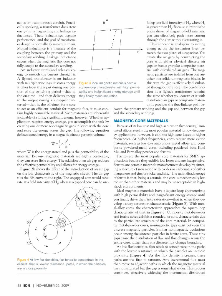
act as an instantaneous conduit. Practi-cally speaking, a transformer does storeenergy in its magnetizing and leakage in-ductances. These inductances degradeperformance, and the goal of transform-er design is normally to minimize them.Mutual inductance is a measure of thecoupling between the primary and thesecondary winding. Leakage inductanceoccurs when the magnetic flux does notfully couple to the secondary winding.
An inductor stores and releases en-ergy to smooth the current through it.A flyback transformer is an inductorwith multiple windings; it stores energyit takes from the input during one por-tion of the switching period—that is,the on-time—and then delivers energyto the output during a subsequent in-terval—that is, the off-time. For a coreto act as an efficient conduit for magnetic flux, it must con-tain highly permeable material. Such materials are inherentlyincapable of storing significant energy, however. When an ap-plication requires energy storage, you accomplish the task bycreating one or more nonmagnetic gaps in series with the coreand store the energy across the gap. The following equationdefines stored energy in a magnetic circuit per unit volume:
WB
= ×21
2,
μwhere W is the energy stored and � is the permeability of thematerial. Because magnetic materials are highly permeable,they can store little energy. The addition of an air gap reducesthe effective permeability and allows for energy storage.
Figure 2b shows the effect of the introduction of an air gapon the BH characteristic of the magnetic circuit. The air gaptilts the BH curve to the right. The ungapped core would satu-rate at a field intensity of H1, whereas a gapped core can be use-
ful up to a field intensity of H2, where H2is greater than H1. Because current is theprime driver of magnetic-field intensity,you can effectively push more currentthrough the core without saturating it.
This concept is analogous to storingenergy across the insulation layer be-tween the two plates of a capacitor. Youcreate the air gaps by constructing thecore with either physical discrete airgaps or from a granular composite mate-rial with distributed air gaps. The mag-netic particles are isolated from one an-other in a solid, nonmagnetic binder. Inthis way, the gap is effectively distribut-ed throughout the core. The core’s func-tion in a flyback transformer remainsthe same whether you construct it withdistributed air gaps or composite materi-al: It provides the flux-linkage path be-
tween the primary winding and the gap and between the gapand the secondary windings.
MAGNETIC-CORE MATERIALSBecause of its low cost and high-saturation flux density, lami-
nated silicon steel is the most popular material for low-frequen-cy applications; however, it exhibits high core losses at higherfrequencies. At higher frequencies, cores require more exoticmaterials, such as low-loss amorphous metal alloys and com-posite powdered-metal cores, including powdered iron, KoolMu, and Permalloy powder and ferrites.
Ferrites are the most popular core materials for SMPS ap-plications because they exhibit low losses and are inexpensive.Ferrites are ceramic materials manufacturers develop by sinter-ing a mixture of iron oxide with oxides or carbonates of eithermanganese and zinc or nickel and zinc. The main disadvantageof ferrite is that, being a ceramic, the core is mechanically lessrobust than other materials and may be unacceptable in high-shock environments.
Ideal magnetic materials have a square-loop characteristicwith high permeability and insignificant energy storage untilyou finally drive them into saturation—that is, when they de-velop a sharp saturation characteristic (Figure 3). With met-al-alloy cores, the characteristic approaches the square-loopcharacteristic of that in Figure 3. Composite metal-powderand ferrite cores exhibit a rounded, or soft, characteristic dueto the particulate structure of the core material. In compos-ite metal-powder cores, nonmagnetic gaps exist between thediscrete magnetic particles. Similar nonmagnetic occlusionsoccur among the sintered particles in ferrite cores. These tinygaps cause the distribution of flux and flux changes across theentire core, rather than at a discrete flux-change boundary.
At low flux densities, flux tends to concentrate in the pathswith the lowest resistance, in which the particles are in closeproximity (Figure 4). As the flux density increases, thesepaths are the first to saturate. Any incremental flux mustthen move to adjacent paths in which the magnetic materialhas not saturated but the gap is somewhat wider. This processcontinues, effectively widening the incremental distributed
B
H
Figure 3 Ideal magnetic materials have asquare-loop characteristic with high perme-ability and insignificant energy storage untilthey finally reach saturation.
×
ו••
×
Figure 4 At low flux densities, flux tends to concentrate in theeasiest—that is, lowest-resistance—paths, in which the particlesare in close proximity.
38 EDN | NOVEMBER 26, 2009
edn091102ms4346_ID 38edn091102ms4346_ID 38 11/12/2009 9:46:46 AM11/12/2009 9:46:46 AM
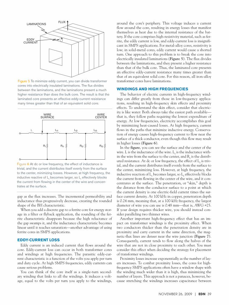
gap as the flux increases. The incremental permeability andinductance thus progressively decrease, creating the roundedshape of the BH characteristic.
When you add a discrete gap to a ferrite core for energy stor-age in a filter or flyback application, the rounding of the fer-rite characteristic disappears because the high reluctance ofthe gap swamps it, and the inductance characteristic becomeslinear until it reaches saturation—another advantage of usingferrite cores in SMPS applications.
EDDY-CURRENT LOSSEddy current is an induced current that flows around the
core. Eddy-current loss can occur in both transformer coresand windings at high frequencies. The parasitic eddy-cur-rent characteristic is a function of the volts you apply per turnand duty cycle. At high SMPS frequencies, eddy currents cancause serious problems.
You can think of the core itself as a single-turn second-ary winding that links to all the windings. It induces a volt-age, equal to the volts per turn you apply to the windings,
around the core’s periphery. This voltage induces a currentflow around the core, resulting in energy losses that manifestthemselves as heat due to the internal resistance of the bat-tery. If the core comprises high-resistivity material, such as fer-rite, the eddy current is low, and eddy-current loss is insignifi-cant in SMPS applications. For metal-alloy cores, resistivity islow; in solid-metal cores, eddy current would cause a shortedturn. One approach to this problem is to break the core intoelectrically insulated laminations (Figure 5). The flux dividesbetween the laminations, and they present a higher resistancethan that of the bulk core. Thus, the laminated core presentsan effective eddy-current resistance many times greater thanthat of an equivalent solid core. For this reason, all iron-alloytransformer cores have laminations.
WINDINGS AND HIGH FREQUENCIESThe behavior of electric currents in high-frequency wind-
ings can differ greatly from those in low-frequency applica-tions, resulting in high-frequency skin effects and proximityeffects. To understand the skin effect, consider that electric-ity is like water: Both always take the easiest path available—that is, they follow paths requiring the lowest expenditure ofenergy. At low frequencies, electricity accomplishes this goalby minimizing heat-caused losses. At high frequency, currentflows in the paths that minimize inductive energy. Conserva-tion of energy causes high-frequency current to flow near thesurface of a thick conductor, even though this flow may resultin higher losses (Figure 6).
In the figure, you can see the surface and the center of thewire. L is the inductance of the wire. LI is the inductance with-in the wire from the surface to the center, and RI is the distrib-uted resistance. At dc or low frequency, the effect of LI is triv-ial, and the current distributes itself evenly from the surface tothe center, minimizing loss. However, at high frequency, theinductive reaction of LI becomes larger, so LI effectively blocksthe current from flowing in the center of the wire, and it con-centrates at the surface. The penetration, or “skin,” depth isthe distance from the conductor surface to a point at whichthe current density is one electric-field current times the sur-face current density. At 100 kHz in copper, penetration depthis 0.24 mm, meaning that, at a 100-kHz frequency, the largestdiameter of wire you can use is 0.48 mm—that is, AWG #25.If your design requires thicker wire, you should instead con-sider paralleling two thinner wires.
Another important high-frequency effect that has an im-pact on transformer windings is the proximity effect. Whentwo conductors thicker than the penetration density are inproximity and carry current in the same direction, the mag-netic-flux lines are denser near the wire junction (Figure 7).Consequently, current tends to flow along the halves of thewire that are not in close proximity to each other. You mustconsider this effect when deciding the strategy for placementof transformer windings.
Proximity losses increase exponentially as the number of lay-ers increases. To combat proximity losses, the cores for high-frequency SMPS applications often have a window shape withthe winding much wider than it is high, thus minimizing thenumber of layers. This approach is not a panacea, however, be-cause stretching the windings increases capacitance between
FLUXLAMINATIONS
EDDYCURRENT
Figure 5 To minimize eddy current, you can divide transformercores into electrically insulated laminations. The flux dividesbetween the laminations, and the laminations present a muchhigher resistance than does the bulk core. The result is that thelaminated core presents an effective eddy-current resistancemany times greater than that of an equivalent solid core.
RI
LI1 LI2 LI3
RI1 RI2 RI3
L
WIRESURFACE
WIRECENTER
Figure 6 At dc or low frequency, the effect of inductance istrivial, and the current distributes itself evenly from the surfaceto the center, minimizing losses. However, at high frequency, theinductive reactive of LI becomes larger, so LI effectively blocksthe current from flowing in the center of the wire and concen-trates at the surface.
NOVEMBER 26, 2009 | EDN 39
edn091102ms4346_ID 39edn091102ms4346_ID 39 11/12/2009 9:46:47 AM11/12/2009 9:46:47 AM

them. An interleaving winding strategy,on the other hand, alternately places theprimary and secondary windings on topof each other, avoiding the need for anelongated window. Contrary to popularbelief, in high-frequency SMPSs, it is of-ten better to leave the window area un-used rather than pack it with copper toreduce dc resistance. The increased layerscan increase ac losses by as much as 10times as compared with dc losses.
OTHER CONSIDERATIONSMinimizing losses is vital to SMPS de-
sign, but minimizing EMI (electromag-netic interference) is also critical. Onecause of EMI is interwinding capacitancethat couples common-mode noise fromthe primary to the secondary windings.You can reduce this capacitance by us-ing a Faraday shield—a thin foil or met-allized film in the intervening space between the primary andsecondary windings. The shield should be thinner than thepenetration density to avoid eddy-current losses and shouldconnect to the low-impedance—that is, nonswitching—nodeof the transformer’s primary. Special winding configurations,such as those that Power Integrations (www.powerint.com)
developed, can also reduce EMI (Ref-erence 1). The unterminated windingson the transformer act as electrostat-ic shields within the transformer. Thetransformer shields cancel some of theswitching signals, significantly attenu-ating the composite signal across theparasitic capacitance and significantlyreducing the transformer’s parasitic (ca-pacitive) coupling paths (Figure 8).
Core hysteresis, eddy-current, andwinding losses, which generate temper-ature rise, occur in all transformers. Inbuck-derived applications, under fixed-frequency operation, volt seconds andflux swing are constant. Hysteresis loss istherefore constant, regardless of chang-es in input voltage or load current. Coreeddy-current loss is proportional to theinput voltage; thus, worst-case loss oc-curs at high input voltages. Winding
losses are proportional to the duty cycle, which is greatest atlow input voltage.
SMPS designers must select cores that will remain within asafe working temperature under any of these worst-case condi-tions. They should also consider start-up and transients whena sudden increase in load current occurs. The control loop
xx
xx
xx
xx
xx
xx
xxx
xxx
xxx
xxx
xxx
xxx
MAGNETIC-FLUX DISTRIBUTION
CURRENT TENDS TO FLOWALONG HALVES NOT IN
CLOSE PROXIMITY
Figure 7 When two conductors thickerthan the penetration depth are in proximityand carry current in the same direction, themagnetic-flux lines are denser near the wirejunction. Consequently, current tends toflow along the halves of the wire that arenot in close proximity to each other.
40 EDN | NOVEMBER 26, 2009
edn091102ms4346_ID.indd 40edn091102ms4346_ID.indd 40 11/12/2009 10:46:02 AM11/12/2009 10:46:02 AM

Figure 8 The unterminated windings on the transformer act aselectrostatic shields within the transformer, canceling some ofthe switching signals, attenuating the composite signal acrossthe parasitic capacitance, and reducing the transformer’s para-sitic (capacitive) coupling paths.
SECONDARY
14
NC
1
32
85
BALANCING SHIELDWINDING
PRIMARY WINDING
CORE CANCELLATIONWINDING
calls for full current, pushing the duty cycle to its absolute-maximum limit. If the input voltage is at the maximum, thevolt seconds you apply to the transformer windings could beseveral times larger than normal, driving the core into satura-tion. Fortunately, modern control ICs include soft-start andsophisticated current- or volt-second-limiting circuitry to pro-tect the system from both operational and fault conditions.
To design a flyback transformer for an SMPS, first define thecircuit parameters and select the core material and geometry.Next, determine the peak current in the circuit and the maxi-
mum flux density and flux swing. After making those deter-minations, tentatively select the core’s shape and size and de-termine the loss limit for flux density or core losses. You thencalculate the number of turns, the gap length, the conductorsize, and the winding resistance. Last, calculate flux density,winding loss, total loss, and temperature rise and then adjustthese values to the size of the core. Available software, such asPI Expert from Power Integrations, can help with this process(Reference 2). The available packages can automate power-supply design, including component selection and transform-er design, enabling even less-experienced design engineers tosuccessfully complete an SMPS design that complies with in-ternational standards for efficiency, safety, and EMI. Detailedknowledge of magnetics is not necessary, but it helps to have abasic understanding of what the software is doing.EDN
R E FE R E N CE S1 “Power Supply Design” and “PI Expert Support” technicalforums, www.powerint.com//forum/ask-pi-engineer.2 “PI Expert Design Software,” www.powerint.com/pi-expert.
AUTH OR’S B I OG RAPHYSameer Kelkar is a senior applications engineer at Power Integra-tions, where he designs and develops tools, design ideas, and refer-ence-design kits for the company’s products. He also provides tech-nical support to internal divisions to ensure product quality. Kelkarhas a master’s degree in electrical engineering from the University ofMinnesota (Minneapolis, MN).
GAIN Experience. SAVE Time.Your Power Questions Answered in the Lab
View Videos Now at
vicorpower.com/PT3
EMI: How to Get the Lowest Noise
Thermal & Mechanical Considerations
Input Overvoltage Protection
Improving Output Filtering
Vicor's PowerTechtorial Series concentrateson important, real-world technical issues in power system design. Power questions are answered by senior applications engineers through concise, expert instruction in the lab. Gain access to view anever-growing number of Vicor PowerTechtorialvideos at vicorpower.com/PT3 . Vicor Applications Engineering: 800-927-9474
PO ERTECHTORIALS™
edn091102ms4346_ID.indd 41edn091102ms4346_ID.indd 41 11/12/2009 10:49:28 AM11/12/2009 10:49:28 AM

42 EDN | NOVEMBER 26, 2009
Solar cells convert light energyinto electricity, making them
a renewable energy source. Solar-cellmanufacturers often use SEMs (scan-ning electron microscopes) to detectdefects in solar cells while they’re stillin wafer form. Although SEMs can seedown to a solar cell’s grain structure,they can be slow because their scan ar-ea is small. A SEM must scan a wafermany times to cover it.
Instead of using a SEM, you can usean SWIR (shortwave-infrared) cam-era system to detect defective cells.You can take advantage of a solar
cell’s electroluminescence signatureto find defects on a solar cell. A cell’slight has a wavelength of about 1.1 mi-cron, which results when you apply aforward bias voltage and forward op-erating current of at least 7A to thecell. An SWIR sensor can provide animage of an entire wafer, eliminatingthe need to scan the wafer. The sensoridentifies defects by detecting a wafer’selectroluminescence.
Figure 1 shows the system, whichuses an SWIR sensor that converts animage into an analog voltage. A pre-amplifer boosts the signal to a level suf-
ficient for an ADC in a digital-process-ing module to digitize the analog signalat 10M samples/sec.
The ADC’s digital output travelsthrough an LVDS (low-voltage-dif-ferential-signaling) data interface to aDalsa (www.dalsa.com) frame-grabbercard in a computer. Custom image-processing software, written in C��,processes the data, producing an imageof the entire wafer on the computer’sscreen.
The board containing the sensor,preamplifier, and ADC also has a mi-crocontroller, which generates a clocksignal for the timing of the sensor andthe ADC. An RS-232 communica-
READERS SOLVE DESIGN PROBLEMS
EDITED BY MARTIN ROWEAND FRAN GRANVILLE
designideasInspect solar cellswithout a microscope
Figure 1 An ADC digitizes an analog signal from an SWIR sensor and sendsthe signal to a frame grabber for processing.
5 AND 3.3VPOWER-SUPPLY
CIRCUIT
PREAMPLIFIERCIRCUIT
TIMING-DRIVERCIRCUIT
900- TO 1700-NMSWIR AREA
CHARGE-COUPLEDDEVICE
TIMING-GENERATORCIRCUIT
MAIN CLOCKCIRCUIT
MICROCONTROLLER(RS-232 INTERFACE)
ADCIMAGE-GRABBING
CARD(LVDS INTERFACE)
IMAGE-DATA GRAB
FOUR-PINCOMMAND PORT
INTEGRATION-TIMECONTROL
CHARGE-COUPLED-DEVICE FOCAL-PLANE ARRAY
DIGITAL PROCESSING
POWER
�
DIs Inside43 Solar-powered sensorcontrols traffic
46 Self-oscillating H bridge lightswhite LED from one cell
48 Low-cost LCD-bias genera-tor uses main microcontrolleras control IC
�To see all of EDN ’s DesignIdeas, visit www.edn.com/designideas.
Chun-Fu Lin and Tai-Shan Liao,National Applied Research Laboratories, Hsinchu, Taiwan
Figure 2 An electroluminescenceimage of solar cells shows darkareas that indicate failed cells.
edn091102di_id 42edn091102di_id 42 11/12/2009 11:13:36 AM11/12/2009 11:13:36 AM

NOVEMBER 26, 2009 | EDN 43
Have you ever sat in your carwaiting for the light to turn
green when nobody’s using the crossstreet? This wait is due to the factthat the sensors controlling these traf-fic signals—in one large-suitcase-sizedbox per intersection—are classically
dumb, with relays, cams, and switch-es, although they now may includesoftware that accepts data from localsensors, automobile-sized inductiveloops buried in the asphalt. Moderncontrollers have gained some intel-ligence. For example, they may share
tions port on the Atmel (www.atmel.com) microcontroller allows it to com-municate with a PC to get commandsfrom the user who set parameterssuch as the SWIR sensor’s operatingmode. A timing-driver circuit sends
the clock signal to the SWIR sensor.Figure 2 shows the image from the
SWIR camera circuit. This imageshows the intensity distribution of thecell’s light output. A homogenous in-tensity-distribution image is essential
for a high-quality solar cell, but solarcells always show some inconsistencies.All defects resulting in a local reduc-tion of the carrier concentration arevisible on the electroluminescence im-age as dark bars.EDN
Solar-powered sensor controls trafficLarry K Baxter, Capsense, Lexington, MA
�
6V, 900-mASOLAR CELL
BQ24083RBATTERY CHARGER
3V, 19-AHRLITHIUM BATTERY
LOW-DROPOUTREGULATOR, SWITCH
3V SWITCHED3V
STRIP-DETECTORPNEUMATIC
TWOPRESSURESENSORS
INSTRUMENTATIONAMP INA333
MEASURE VOLTAGES
2.4-GHzCC2500
WIRELESSTRANSCEIVER1.5V OPA333
GENERATOR
MOVINGWEIGHT TMP102
TEMPERATURESENSOR
WIM-DETECTORCAPACITIVE
CAP PAD
CAPACITIVESENSOR
WEIGHT
DRIVE
940-nm LED FET
IR-BEAMINTERRUPT
SWITCH,LED
MSP430F248
MICROCONTROLLER
PINPHOTODIODE
OPA364AMP
DAC6311DAC
PGA112PROGRAMMABLE-
GAIN AMP
OPA364AMP
MOVING IR
PASSIVE-INFRAREDDETECTOR
NOTE: ITEMS IN BOLDFACE ARE ON THE IRON CIRCUIT DESIGNERCONTEST APPROVED-PARTS LIST.
Figure 1 Most of the circuit amplifies outputs from four sensors, digitizes them with the MSP430’s 12-bit ADC, does somepreprocessing, and messages the controller.
THIS DESIGN WASWINNING ENTRY INEDN’s RECENT ONLINEIRON CIRCUITDESIGNER CONTEST;see the completedesign at www.edn.com/091126dia
edn091102di_id 43edn091102di_id 43 11/12/2009 11:13:37 AM11/12/2009 11:13:37 AM

44 EDN | NOVEMBER 26, 2009
designideas
data with nearby inter-sections, respond to radiorequests from emergencyvehicles, and sometimestake commands from atraffic-control center. ThisDesign Idea describes theTSP (traffic-sensor post),a more accurate, effective,inexpensive, and easy-to-install approach to moni-t oring traffic flow. Thesesensors measure vehicle lo-cation and speed in four ormore streets at an intersec-tion or at a distance fromthe intersection for early warning. Asecond application of this technology,the WIM (weight-in-motion) sensor,weighs moving trucks.
The circuit comprises a wireless,solar-powered sensor array that handlesall the data collection at an intersec-tion (Figure 1). Cities can install thesesensors at each of the four corners ofan intersection for full coverage. Thesensors send data to the single control-ler box over IEEE 802.15.4 in a starnetwork. The approach combines foursensors in an inexpensive, low-mainte-nance, 6-in.-diameter, 6-foot-tall post.You can build the circuit into the postthat holds the traffic lights, or you canuse it stand-alone. Not all TSPs requireall four sensors; you can select thosethat your application needs based onusage. The TSP is the first wireless ap-proach to this problem, and one of thesensors, the Cap Pad, provides a hugeadvantage over current expensive andinaccurate WIM sensors (Figure 2).
The TSP uses a PIR (passive-infra-red) sensor that looks 10 microns into
the deep-IR band for moving IR sourc-es. This technology finds use in inex-pensive motion-detecting lamp con-trols and senses vehicles from 30 feetaway. The detection range is good, theparts are cheap, and the beam can seethrough a layer of dirt. It can’t measurespeed, distance, or direction.
The TSP also uses conventionalpneumatic tubes. Rubber tubes are sta-pled to the asphalt and feed two pres-sure sensors. This approach accuratelymeasures speed, but permanent instal-lations cannot use it because it getsdamaged easily. Municipalities oftendeploy pneumatic tubes to measuretraffic volume in road construction.
The Cap Pad comprises a 10-in.�12-foot sandwich of three 0.05-in.-thickstainless-steel sheets separated by two0.05-in.-diameter closed-cell urethane-foam layers (Figure 3). You capacitive-ly measure the 0.025-in. deflection ofthe pad under a truck’s tire to weighthe axle. One Cap Pad can handlethe WIM requirements, and using twocan add speed and direction informa-
tion. You use multiple pads to handlemultilane roads. The Cap Pad can befastened to the asphalt with adhesiveor pavement tape or buried under asmuch as an inch of asphalt for protec-tion. Its materials cost is only a couplehundred dollars, a huge saving over thepiezoelectric WIM sensors currently inuse.
The TSP also uses a near-IR trans-mitter/receiver using a pulsed LED fortransmission and a PIN (positive-in-trinsic-negative) photodiode for re-ception. Both need cylindrical lensesto focus the beam to a 2�-wide, 5�-highellipse that covers a remote retrore-flective screen, as in highway signs, orto the IR sensors on another TSP. Amultilayer optical bandpass filter thatremoves visible light further improvesthe range.
Precision capacitive sensors can mea-sure an air gap between adjacent metalplates to subnanometer accuracy. Un-fortunately, accuracy in the WIM appli-cation requires flat and parallel surfaces,and the Cap Pad has neither. Capaci-tive sensors can also accurately measurea force on adjacent flat plates with a re-storing spring, but flatness and parallel-ism are still requirements. Maintainingparallelism over a 10-in. pad would bedifficult, and roads are seldom flat.
If compression of the air pockets inclosed-cell foam provides the restor-ing force, however, the resulting springconstant changes from the convention-al F�K�x of springs or cantileveredbeams to F�P0�H/(H�x), where Fis force, P0 is atmospheric pressure,H is the starting gap, and x is the dis-
STEEL
CLOSED-CELLURETHANE FOAM
0.25 IN.
Figure 3 The Cap Pad sensor is a 10-in.�12-foot sandwich of three 0.05-in.-thick stainless-steel sheets separated by two 0.05-in.-diameter closed-cellurethane-foam layers.
J4
P3
CP24 nF
CAP PAD
4
3
2
1
10-mSEC MINIMUM PULSE30-mV CAPACITIVE SENSOR
D11N5333
Q1
R14100k
R152k
C13220 pF
ESD
EMS
863-1N5228BG
RC=100 �SEC
D
G
S QMN-2N7002
CAP PAD
CAP DRIVE
T=R�CP
Figure 2 The Cap Pad sensor has a nominal capacitance of about 24 nF at rest, with achange of about 7% full-scale when a truck passes.
edn091102di_id 44edn091102di_id 44 11/12/2009 11:13:39 AM11/12/2009 11:13:39 AM

Integrates Li+ charger, Smart Power Selector™, three step-down converters, and a WLED step-up converter in a tiny 4mm x 4mm package
Smart Power Selector is a trademark of Maxim Integrated Products, Inc.*U.S. Patent #6,507,172.
Industry’s smallestpower-management IC for
portable media players
USB/AC-TO-DCADAPTER
ENABLE SYSTEM
ENABLE CHARGER
ENABLE BACKLIGHT
SYS
DC
EN123
CEN
EN4
LX4
OVP4
FB4GND
OUT3
OUT2
BAT
SYS
Li+/Li-PolyBATTERY
I/O
MEMORY
CORE
OUT1
MAX8819
“Instant-on” response: Smart Power Selector shares system and battery power, enabling
operation with dead or no battery
Maximizes battery life: three 95% efficient,
2MHz step-downconverters
Travel light: advanced USB charger* eliminates bulky adapter, meets USB
2.0 specifications
Dimming control: high-efficiency step-up converter drives
2 to 6 WLEDs
Evaluation kit~88mm2 solution area, 1mm solution height
(Form-factor-optimized placement)
11.6mm
7.6m
m
2016
4mm x 4mm1608 1608
1005
06030603
0603
0603 RESCAP
IC
DIODE
LEGEND
INDUCTOR
0603
1608 1608
2220
2016
2012 16
08
1608
1608
1608
1608
1608
2016
MAX8819
28-TQFN
4mm
x 4m m x 0.8m
m
Innovation Delivered is a trademark and Maxim is a registered trademark of Maxim Integrated Products, Inc. © 2009 Maxim Integrated Products, Inc. All rights reserved.
www.em.avnet.com/maxim
™DIRECTwww.maxim-ic.com/shop
For free samples or technical support, visit our website.
www.maxim-ic.com/MAX8819-info
TM
edn091102.indd 45edn091102.indd 45 11/5/2009 1:51:20 PM11/5/2009 1:51:20 PM
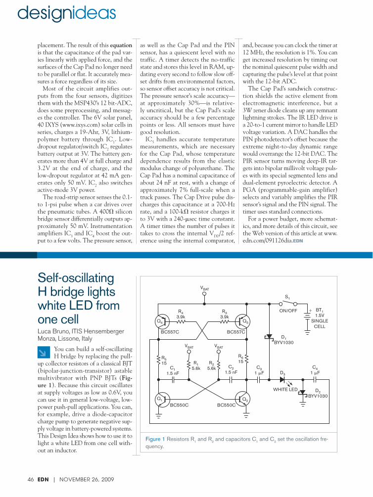
46 EDN | NOVEMBER 26, 2009
You can build a self-oscillatingH bridge by replacing the pull-
up collector resistors of a classical BJT(bipolar-junction-transistor) astablemultivibrator with PNP BJTs (Fig-ure 1). Because this circuit oscillatesat supply voltages as low as 0.6V, youcan use it in general low-voltage, low-power push-pull applications. You can,for example, drive a diode-capacitorcharge pump to generate negative sup-ply voltage in battery-powered systems.This Design Idea shows how to use it tolight a white LED from one cell with-out an inductor.
designideas
placement. The result of this equationis that the capacitance of the pad var-ies linearly with applied force, and thesurfaces of the Cap Pad no longer needto be parallel or flat. It accurately mea-sures a force regardless of its size.
Most of the circuit amplifies out-puts from the four sensors, digitizesthem with the MSP430’s 12 bit-ADC,does some preprocessing, and messag-es the controller. The 6V solar panel,40 IXYS (www.ixys.com) solar cells inseries, charges a 19-Ahr, 3V, lithium-polymer battery through IC1. Low-dropout regulator/switch IC2 regulatesbattery output at 3V. The battery gen-erates more than 4V at full charge and3.2V at the end of charge, and thelow-dropout regulator at 42 mA gen-erates only 50 mV. IC2 also switchesactive-mode 3V power.
The road-strip sensor senses the 0.1-to 1-psi pulse when a car drives overthe pneumatic tubes. A 400� siliconbridge sensor differentially outputs ap-proximately 50 mV. Instrumentationamplifiers IC3 and IC4 boost the out-put to a few volts. The pressure sensor,
as well as the Cap Pad and the PINsensor, has a quiescent level with notraffic. A timer detects the no-trafficstate and stores this level in RAM, up-dating every second to follow slow off-set drifts from environmental factors,so sensor offset accuracy is not critical.The pressure sensor’s scale accuracy—at approximately 30%—is relative-ly uncritical, but the Cap Pad’s scaleaccuracy should be a few percentagepoints or less. All sensors must havegood resolution.
IC5 handles accurate temperaturemeasurements, which are necessaryfor the Cap Pad, whose temperaturedependence results from the elasticmodulus change of polyurethane. TheCap Pad has a nominal capacitance ofabout 24 nF at rest, with a change ofapproximately 7% full-scale when atruck passes. The Cap Drive pulse dis-charges this capacitance at a 700-Hzrate, and a 100-k� resistor charges itto 3V with a 240-�sec time constant.A timer times the number of pulses ittakes to cross the internal VDD/2 ref-erence using the internal comparator,
and, because you can clock the timer at12 MHz, the resolution is 1%. You canget increased resolution by timing outthe nominal quiescent pulse width andcapturing the pulse’s level at that pointwith the 12-bit ADC.
The Cap Pad’s sandwich construc-tion shields the active element fromelectromagnetic interference, but a3W zener diode cleans up any remnantlightning strokes. The IR LED drive isa 20-to-1 current mirror to handle LEDvoltage variation. A DAC handles thePIN photodetector’s offset because theextreme night-to-day dynamic rangewould overrange the 12-bit DAC. ThePIR sensor turns moving deep-IR tar-gets into bipolar millivolt voltage puls-es with its special segmented lens anddual-element pyroelectric detector. APGA (programmable-gain amplifier)selects and variably amplifies the PIRsensor’s signal and the PIN signal. Thetimer uses standard connections.
For a power budget, more schemat-ics, and more details of this circuit, seethe Web version of this article at www.edn.com/091126dia.EDN
Self-oscillatingH bridge lightswhite LED fromone cellLuca Bruno, ITIS HensembergerMonza, Lissone, Italy
� R615
D1BYV1030
D2BYV1030
R515 R1
5.6kR2
5.6kC11.5 nF
C21.5 nF
C31 �F
C41 �FD3
R43.9k
R33.9k
Q4 Q3
S1
Q1 Q2
BC557C
BC550C BC550C
BC557C
VBAT
VBAT VBAT
WHITE LED
ON/OFF BT11.5V
SINGLECELL
�
Figure 1 Resistors R1 and R2 and capacitors C1 and C2 set the oscillation fre-quency.
edn091102di_id 46edn091102di_id 46 11/12/2009 11:13:40 AM11/12/2009 11:13:40 AM

Smallest low-frequency RF productshave highest performance and
efficiency with lowest current draw
RKE
SECURITYSYSTEMS
HOMEAUTOMATION
RADIO-CONTROLLEDTOYS
300MHz to 450MHz Transmitters
Part FeaturesMaxim
Package Area (mm2)
Closest Competition Package Area
(mm2)
Maxim CurrentConsumption
(mA)
ClosestCompetitionCurrent (mA)
Maxim Tx Power
(dBm, max)
Closet Competition Tx Power
(dBm, max)
MAX1472 ASK 9 32 9.1 14 10 10MAX7044 ASK, clock output 9 32 13.8 14 13 10
MAX7057/MAX7058
Frac-N programmable frequency ASK/FSK, dual-frequency ASK 60 50 8.5mA ASK,
13mA FSK 17 10 10
300MHz to 450MHz Receivers
Part Features Maxim Sensitivity (dBm)
Closest CompetitorSensitivity (dBm)
Maxim Current Consumption (mA)
Closest CompetitorCurrent Consumption (mA)
MAX1473/MAX7033 ASK, 3.3V/5V, AGC, AGC hold (MAX7033) -114/-114 -113 5.5 at 3V 5.0 at 5V
MAX1471 ASK/FSK, polling timer -114 ASK, -108 FSK -113 ASK, -105 FSK 7.0 at 2.4V 5.7 at 5VMAX7042 FSK, 3.3V/5V -110 FSK -97 FSK 7.0 at 2.4V 9.0 at 2.7V
300MHz to 450MHz Transceivers
Part FeaturesMaxim
Package Area (mm2)
Closest Competition Package Area
(mm2)
Maxim Current Consumption
(mA)
Closest Competition Current (mA)
Maxim Tx Power
(dBm, max)
Closest CompetitionTx Power
(dBm, max)
MAX7030/MAX7031/MAX7032
315/345/433.92MHz ASK, 308/315/433.92MHz FSK 25 49 8.5 to 12.5 16 10 10
www.em.avnet.com/maxim
™DIRECTwww.maxim-ic.com/shop
www.maxim-ic.com/LFRF-info
TM
Innovation Delivered is a trademark and Maxim is a registered trademark of Maxim Integrated Products, Inc. © 2009 Maxim Integrated Products, Inc. All rights reserved.
For free samples or technical support, visit our website.
edn091102.indd 47edn091102.indd 47 11/5/2009 1:51:21 PM11/5/2009 1:51:21 PM

48 EDN | NOVEMBER 26, 2009
LCD circuits often require a�10V voltage at 2 to 15 mA to
bias a graphics-LCD-driver IC. You canusually accomplish this task with an ex-ternal charge-pump IC, such as Max-im’s (www.maxim-ic.com) ICL7660,but that approach adds cost to the de-sign. Instead, you can control a buck-boost switch-mode regulator using thesame microcontroller that sends datato the LCD. In addition, you can se-quence the power rails under softwarecontrol, as some types of LCD control-lers require.
The circuit includes IC1, an Atmel(www.atmel.com) Attiny15 micro-controller (Figure 1), which providesregulation with 200-mV-p-p ripple ata 30-mA load current when supplying�10V. Listing 1, which is availablein the online version of this DesignIdea at www.edn.com/091126dib, lets
you download the source code, whichuses only 4.8% of the total CPU timeto achieve the stated regulation, evenwith a relatively low-speed clock fre-quency of 1.6 MHz.
To minimize CPU time, the soft-ware uses the 8-bit on-chip PWM(pulse-width modulator) to drive Q1.With the on-chip ADC in free-run-ning mode, the microcontroller gener-ates a hardware interrupt with a periodof 7.69 kHz. The interrupts have onedrawback: If they stop, the circuit cango out of regulation. Thus, you musttake care when using interrupts withlong processing times. The Attiny15uses an on-chip, 16� PLL (phase-locked loop) to drive the PWM timer.You can achieve a PWM carrier fre-quency of 100 kHz, which allows theuse of a relatively low-capacitance fil-ter capacitor, C1.
designideas
Transistors Q1, Q2, Q3, and Q4 formthe H bridge, which acts as a simplecharge-pump converter and requiresonly two small, inexpensive ceramiccapacitors, C3 and C4, to perform itsfunction. When Q2 and Q4 are on, ca-pacitors C3 and C4 charge to the bat-tery voltage through forward-biasedSchottky diodes D1 and D2. When Q1and Q3 are on, they discharge the ca-pacitors through resistors R5 and R6and the LED. Because this process re-peats at a high rate of speed, the LEDappears always on.
The circuit oscillates with a frequen-cy based on time constants R1C1 andR2C2. During discharge, the voltagethat develops across resistors R5 and R6and the LED remains approximatelyconstant because of the high switch-ing frequency. The measured value,for a nominal 1.5V battery voltage, is3.8V—enough to drive a white LEDwith a forward voltage of 3 to 3.5V.Resistors R5 and R6 set the LED’s peakcurrent and limit the possible current
spikes that a push-pull output stage canproduce.
Choosing the astable oscillator’s fre-quency involves a trade-off betweenthe time necessary to charge capacitorsC3 and C4 and the need to reduce theirdischarge. For a given capacitance val-ue of C3 and C4, you must experimentto find the optimum frequency. Withthe component values in Figure 1, thefrequency and the duty cycle are about66 kHz and 50%, respectively, and theLED’s drive current is a square-wavesignal with 20-mA peak value and 10-mA average value. The LED dims grad-ually as the battery voltage decreases,and the LED is off when the batteryvoltage falls below 0.9V. For high effi-ciency, use small-signal transistors withhigh dc current gain and low collector-to-emitter saturation voltage. Notethat the circuit can drive any type ofLED; in this case, you should increasecurrent-limiting resistors R6 and R5 toachieve the LED-drive current yourapplication requires.EDN
Low-cost LCD-bias generator usesmain microcontroller as control ICTom Hughes, Dannemora, Auckland, New Zealand
�
ForEngineeringAssistance
Call Factoryor send direct
for FREE PICO CatalogCall toll free 800-431-1064
in NY call 914-738-1400Fax 914-738-8225PICO Electronics,Inc.
143 Sparks Ave. Pelham, N.Y. 10803-18889INDUSTRIAL • COTS • MILITARY
See full Catalog immediately
www.picoelectronics.com
DC-D
C Co
nver
ters
2V to
10,
000
VDC
Outp
ut
•Over 2500 Std.DC-DC Converters
•Surface Mount•From 2V to 10,000 VDC Output
•1-300 Watt Modules•Isolated/Regulated/Programmable Models Available
•Military Upgrades Available•Custom Models,
Consult Factory
edn091102di_id.indd 48edn091102di_id.indd 48 11/12/2009 12:11:22 PM11/12/2009 12:11:22 PM

NOVEMBER 26, 2009 | EDN 49
Two constants in the source code letyou alter the bias voltage of the circuit’soutput voltage. These constants em-ploy basic buck-boost-converter theory(Reference 1). The following equationdefines the maximum 8-bit constant,or threshold, that the ADC reads onthe chip: 51.2�{VCC�[(VCC�VMAX)/
(R4�R5)]R5}, where VMAX is the maxi-mum desired output voltage and VCCis the supply voltage. To achieve opti-mum operation, increase the PWM sig-nal’s duty cycle when you need highervoltages. Use the following equationto determine the 8-bit PWM’s value:255�VOUT/(VOUT�VIN)�255, where
VOUT and VIN are the output andinput voltages, respectively. In prac-tice, however, if you keep the currentat less than 2 mA, this requirement isless important.
The circuit can deliver currents thatQ1’s collector current predominantlydelivers. This current is the peak outputcurrent that the circuit can safely de-liver. The following equation calculatesthe current: IOUTMAX�(VIN�0.08)/VOUT,where IOUTMAX is the maximum outputcurrent. If your design needs higher cur-rent, then substitute a BC327 for Q1.Additionally, the inductor should havea maximum rms (root-mean-square)current value of at least twice the peakoutput current and preferably be a low-ESR (equivalent-series-resistance) typeto maximize circuit efficiency.EDN
R E FE R E N CEHart, Daniel W, Introduction to
Power Electronics, First Edition, pg202, Prentice Hall, Oct 25, 1996,ISBN-10: 0023511826, ISBN-13:978-0023511820.
VCC
GND
IC1ATTINY15
R22.2k
L1330 �F
C122 �F
C4100 nF
R110k
VOUT�10V
VCC5V
R510k
R433k
D2BAS70
Q1
BC858ASMD
C3100 nF
(ADC0)PB5
(ADC3)PB4
(ADC2)PB3
(ADC1)PB2
(OCP)PB1
(AREF)PB04
8
1VCC
5V 2
3
7
6
5
Figure 1 An Attiny15 microcontroller provides regulation with 200-mV-p-pripple at a 30-mA load current when supplying �10V.
90°0° 180° 270° 360°
sin
coscos
ssisis nnn
cos
Simply Magnetic.
www.austriamicrosystems.com/AS5215
Built-In Redundancy
Analog Sin/Cosine output
Adjustable output amplitude
150°C ambient temperature
Get your free samples online today!
www.austriamicrosystems.com/AS5215
AS5215 Fail Safe Magnetic Rotary Encoder For Safety Critical Applications
180180° 270270° 3600°°90°0°0°
cos
1
edn091102di_id.indd 49edn091102di_id.indd 49 11/12/2009 11:56:14 AM11/12/2009 11:56:14 AM

50 EDN | NOVEMBER 26, 2009
OPTOELECTRONICS/DISPLAYS
productroundupThermoelectric coolermeets 3000g shock-testing standard
Passing the 3000g shock test, theOptoCooler HV14 thermoelectric
cooler meets requirements for mechanicalshock for military standard 883E Method2002. At 85�C, the high-voltage, heat-pumping thermoelectric module operatesat a 2.7V maximum voltage and pumps1.5W of heat. The device creates a 60�Cmaximum temperature differential be-tween the hot and the cold sides with noheat load, suiting cooling and tempera-ture control of opto electronic devices,including laser diodes, avalanche photo-diodes, and high-brightness LEDs. Avail-able in a 3�3-mm footprint, the Opto-Cooler HV14 costs $18 (1000).Nextreme Thermal Solutions,www.nextreme.com
�
LED driver featurestemperature-managementcontrol
The LM3424 high-brightness LEDdriver with temperature-manage-
ment control supports the use of an on-line design environment. The vendor’sWebench LED Designer tool supportsthe device, which enables lighting de-signers to build thermally reliable sys-tems. The driver works in indoor, out-door, and automotive applications andenables programming of temperature andslope breakpoints, allowing safe opera-tion of the LEDs. During an overtemper-ature condition, the product’s thermal-foldback circuitry reduces the regulatedcurrent through the LEDs. A reducedcurrent dims the LEDs to a programmedrange, and the LEDs remain within thatrange until returning to a safe operatingtemperature. The device can drive asmany as 18 high-brightness LEDs in se-ries with a 2A output current and allowsregulation of currents based on buck,
�
edn091102prod_id.indd 50edn091102prod_id.indd 50 11/12/2009 11:00:09 AM11/12/2009 11:00:09 AM

productmart
This advertising is for new and
current products.
NOVEMBER 26, 2009 | EDN 51
A D V E R T I S E R I N D E X
Company PageAdvance Devices Inc 51austriamicrosystems AG 49BuyerZone C-2Coilcraft 3Digi-Key Corp 1EMA Design Automation 22
30Express PCB 40International Rectifier Corp 5Keil Software 50Linear Technology Corp C-4The MathWorks 17Maxim Integrated Products 45
47Mentor Graphics 8Mill Max Manufacturing Corp 7
Company Page
Mornsun GuangzhouScience & Technolgy Ltd 40Mouser Electronics 4National Instruments 23Numonyx 15Pico Electronics 31
3548
Trilogy Design 51TTI Inc. 32Vicor 29
41Xilinx Inc C-3
EDN provides this index as an additionalservice. The publisher assumes no liabilityfor errors or omissions.
boost, SEPIC, flyback, and buck-boosttopologies. Operating over a 4.5 to75V input range, the PWM controlleroperates at an oscillator frequency ashigh as 2 MHz. Available in a TSSOP-20 package, the LM3424 high-bright-ness LED driver costs $1.75 (1000).National Semiconductor,www.national.com Miniature, 0.5W
LED packagemeasures 3.5 mm2
The miniature, 0.5W OVS5Mx-BCR4 LED package series has a
120� viewing angle and a water-clearlens. The package has a 150-mA pow-er dissipation of 0.48W for white,warm-white, and blue LEDs; 0.51Wfor green LEDs; and 0.33W for red,amber, and yellow LEDs. The devicesprovide 4000-, 4500-, and 5000-mcdluminous intensity for the red, am-ber, and yellow packages, respectively.Luminous flux is 25 lm for the white,warm-white, and green LEDs and 6 lmfor the blue LEDs. The devices oper-ate over a �40 to �100�C tempera-ture range. Measuring 3.5�3.5�1.2mm in a surface-mount housing, theOVS5MxBCR4 series costs 25 cents(1000) in amber, red, and yellow; 45cents for white and warm white; 52cents for blue; and 72 cents for green.Optek Technology,www.optekinc.com
in a maximum 0.007-in. thickness, theprotector sheets have a �30 to �70�Coperating temperature. The protectorsheets cost $1 each.Fujitsu Components America,www.fujitsu.com
Adhesive sheetstarget touchscreenand flat-panel displays
The self-wetting adhesive pro-tector sheets reduce surface
damage to touchscreens and flat-pan-el displays in use or during shipping,preserving the optical quality and ex-tending the life of the touch device. Aself-wetting adhesive applies itself byspontaneously wetting out on smoothsurfaces with no or low finger pressure,adhering to a display or touchscreen.The adhesive provides high shear re-sistance and prevents sheet displace-ment. The repositionable sheets comein antiglare, clear hard-coat, and anti-reflective coated versions of the clearprotector sheets. Optical propertiesof the clear protector sheet include91% transmissivity with 1% haze, andthe antiglare protectors provide 90%transmissivity with 8% haze. Available
�
�
edn091102prod_id.indd 51edn091102prod_id.indd 51 11/12/2009 11:00:12 AM11/12/2009 11:00:12 AM

I had been working as a bench techni-cian for about eight years in the com-pany, so my eyes were experienced inseeing problems in any kind of signal.
One day, one of our best customers,complaining of a “noisy picture,” sent usa well-known company’s TV modulator.Because we were not the authorized re-pair center, we advised the customer thatwe would send it to the nearest autho-rized service shop. Nevertheless, whenwe received the modulator, we hookedit up to a TV set; the noise on the dis-play was evident at first glance. I tooksome readings with my old Hewlett-Packard spectrum analyzer and found
that the inband noise floor was 40 dBbelow that of the video carrier, whereasit should have been 60 dB below—andeven lower with equipment from thisrecognized manufacturer. The out-of-band spectrum, on the other hand, wasexcellent for all signals. We sent the unitto the authorized service shop with ourdescription of the problem.
We received the unit back threeweeks later and were astonished to seethat it was still defective even after theservice shop claimed it had no problem;it was exactly as it was when we sent it.Our engineer called the service shop’stechnicians and told them the whole
story, and they asked us to send the unitback to them. Because we had the unitin hand, however, our engineer askedme to troubleshoot—but not repair—the unit. I deduced that the noise wasinband, meaning that something waswrong with the modulation circuit. Itraced the problem to the video circuitand found that a faulty transistor wasattenuating the video baseband signal.As a result, the AGC (automatic gaincontrol) was boosting the tiny signaland, thus, the noise, explaining whythe out-of-band response was so clean.We noted the problem and sent the unitback to the service shop.
A few days later, our engineer re-ceived a call from the shop. The man-ufacturer’s technician told him that hisshop had found no problem with theunit. Incredulous, our engineer startedto argue about the high inband noiselevel, the noisy picture, and so on. Af-ter a few minutes of arguing, the tech-nician at the shop ended the discus-sion by declaring, “Don’t tell me I amwrong! I checked this modulator on a$50,000 test set!” The technician’s big,expensive digital unit had probably dis-played a “unit complies” message withsome mystic numbers and readings.Our technician asked theirs to ship itback, and we decided to repair the unitat no charge to our customer.
Now that most instruments aredigital, I am suspicious of what theytell me. Do I see a difference betweenthe scope’s sampling rate and the signalrate I measured? I double- and triple-check each response at different set-tings. From this experience, I learnedthat nothing replaces the knowledgeand skill you learn over the years. Akeen eye, some common sense, a gooddeal of logic, and a simple and ap-propriate instrument are worth morethan the most expensive digital appa-ratus you work with as a “pushbutton”operator.EDN
Benoit Léveillé is an RF electronicstechnician in Saint-Eustache, PQ,Canada.
52 EDN | NOVEMBER 26, 2009
BENOIT LÉVEILLÉ • RF ELECTRONICS TECHNICIANT A L E S F R O M T H E C U B E
Afew years ago, I was a repair technician in RF elec-tronics at a service center for cable-TV equip-ment. This equipment included everything fromcommercial satellite receivers and cable amplifi-ers to head-end TV modulators. My co-workersand I worked with old analog spectrum analyzers,
and we interpreted most good and bad signals through visualanalysis with instruments at the appropriate setting and scale.
Hawk eyes, analog equipmenttrump expensive digital test set
DA
NIE
L V
AS
CO
NC
ELL
OS
+ www.edn.com/tales
edn091102tales_ID 52edn091102tales_ID 52 11/11/2009 10:28:37 AM11/11/2009 10:28:37 AM

You are not alone. Serial connec-tivity is no longer just the design domain of communications engi-neers. Today, a growing number of designers in the consumer, auto-motive, industrial control, broad-cast equipment, aerospace and defense markets are being tasked with developing products that em-ploy multi-gigabit serial transceiver technology to communicate with next-generation, high-demanding, high-speed networks.
Today’s quest for more band-width and better efficiency means that many designers like you must quickly get up to speed with the analog nuances of multi-gigabit
serial transceivers. Luckily, Xilinx® has engineered its Targeted Design Platforms to help you.
Over the last two decades, the world’s top telecommunications companies have relied upon Xilinx FPGAs’ mix of logic functionality, high-speed memory, parallel con-nectivity, and serial I/O capabilities to create every generation of mod-ern communications equipment.
With many years of experience serving the communication mar-kets, Xilinx is able to help designers in a broad set of markets to quickly master gigabit serial transceiver technology and leverage it to cre-ate innovative products.
In 2009, Xilinx introduced both of its next-generation FPGA families — the high performance Virtex®-6 family and low-cost Spartan®-6 family providing Xil-inx customers access to a full line of serial transceiver-rich FPGAs that can easily maintain line rates from up to 3.2Gbps in the Spar-tan-6 family, to up to 6.5Gbps in its Virtex-6 LXT devices, all the way beyond 11Gbps in the Vir-tex-6 HXT devices.
What’s more, Xilinx announced this full range of serial connectiv-ity-enabled FPGAs as the founda-tion of its new Targeted Design Platform strategy—combining the full line of transceiver-rich FPGAs with world-class tools, validated IP, reference designs, training, and support all delivered in domain and market specific kits. The Targeted Design Platforms allow custom-ers to get their products to market faster than ever before.
With the ISE® Design Suite, customers can now get started on their designs targeting Virtex-6 HXT devices, as well as enhanced support for Spartan-6 LXT and Virtex-6 LXT and Virtex-6 SXT devices. Over the next several months, Xilinx will deliver a num-ber of connectivity enabled de-sign kits targeting wired, wireless broadcast video, packet processing, and traffic management applica-tion using either Virtex-6 devices for high performance, or Spartan-6 devices for low cost.
To learn more, visit the Con-nectivity Page at www.xilinx.com/connectivity where you’ll find documentation, videos, links to software and IP downloads, and much more for helping you get up to speed no matter which fast lane you’re on.
A D V E R T I S E M E N T
BY PANCH CHANDRASEKARAN
re you being asked to make your next-generation product design connect to a high-bandwidth network with an unfamil-iar or a yet-to-be-defined protocol? Are you making the transition from parallel to serial
I/O chip-to-chip communications? Or do you just need the highest-serial bandwidth, most reliable multi-gigabit transceivers the industry has to offer?
AGet Up to Speed with Multi-Gigabit Serial Transceivers
About the Author: Panch Chandrasek-aran is the Sr. Product Marketing Man-ager at Xilinx Inc. (San Jose, Calif.). Contact him at [email protected]
MAINSTREAM HIGH-END ULTRA HIGH-END
Wired
VideoBroadcast
Wireless
Consumer
Automotive
MA
RK
ET S
EGM
ENTS
EDN091102covers.indd 00C3EDN091102covers.indd 00C3 11/5/2009 1:45:13 PM11/5/2009 1:45:13 PM

Isolated RS485
, LTC, LT, LTM and μModule are registered trademarks ofLinear Technology Corporation. All other trademarks are theproperty of their respective owners.
The LTM®2881 is an isolated RS485 transceiver that guards against large ground-to-ground differentials. The LTM2881’sinternal inductive isolation barrier breaks ground loops by isolating the logic level interface and line transceiver. An onboardDC/DC converter provides power to the transceiver with an isolated 5V supply output for powering additional system circuitry.With 2500VRMS galvanic isolation, onboard secondary power and a fully compliant RS485 transmitter and receiver, the LTM2881requires no external components and provides a tiny, complete μModule solution for isolated serial data communications.
Info & Free SamplesFeatures
www.linear.com/2881
1-800-4-LINEAR
• Isolated RS485/RS422 Transceiver:2500VRMS
• Integrated Isolated, Low EMIDC/DC Converter- Up to 500mW Surplus Power
• 3.3V or 5V Input Supply Voltage(LTM2881-3/LTM2881-5)
• 20Mbps or Low EMI 250kbps Data Rate• High ESD: ±15kV HBM• Common Mode Transient Immunity:
30kV/μs• Integrated Selectable 120 Termination• Small Footprint, Low Profile
(11.25mm x 15mm x 2.8mm) inSurface Mount LGA & BGA Packages
LTM2881 Demo Board
3.3V or 5V
5V500mW
RS485/RS422Bus
RO
DI
ON
REG
Galvanic Isolation
Isolated Power
LTM2881
Complete 20Mbps μModule® Transceiver Includes 2500VRMS Isolated Power—No External Components Required
EDN091102covers.indd 00C4EDN091102covers.indd 00C4 11/5/2009 1:45:14 PM11/5/2009 1:45:14 PM