flash memory overview - university of california, san diego€¦ · 111111111111111 111111111111111...
TRANSCRIPT

Flash Memory Overview
Steven Swanson

2
Humanity processed 9 Zettabytes in 2008*
Welcome to the Data Age!
*http://hmi.ucsd.edu

3
Solid State Memories
• NAND flash– Ubiquitous, cheap
– Sort of slow, idiosyncratic
• Phase change, Spin torque MRAMs, etc.– On the horizon
– DRAM-like speed
– DRAM or flash-like density

4
1
10
100
1000
10000
100000
1000000
1 10 100 1000 10000 100000 1000000 10000000
Ban
dw
idth
Re
lati
ve t
o d
isk
1/Latency Relative To Disk
Hard Drives (2006) PCIe-Flash (2007)
PCIe-PCM (2010)
PCIe-Flash (2012)
PCIe-PCM (2013?)
DDR Fast NVM (2016?)
5917x 2.4x/yr
7200x 2.4x/yr

55
Disk Density1 Tb/sqare inch

66
Hard drive Cost
• Today at newegg.com: $0.04 GB ($0.00004/MB)
• Desktop, 2 TB

77
Why Are Disks Slow?
• They have moving parts :-(– The disk itself and the a head/arm
• The head can only read at one spot.
• High end disks spin at 15,000 RPM– Data is, on average, 1/2 an revolution away:
2ms
– Power consumption limits spindle speed
– Why not run it in a vacuum?
• The head has to position itself over the right “track”– Currently about 150,000 tracks per inch.
– Positioning must be accurate with about 175nm
– Takes 3-13ms

88
Making Disks Faster
• Caching
– Everyone tries to cache disk accesses!
– The OS
– The disk controller
– The disk itself.
• Access scheduling
– Reordering accesses can reduce both rotational and seek latencies
99
RAID!
• Redundant Array of Independent (Inexpensive) Disks
• If one disk is not fast enough, use many– Multiplicative increase in bandwidth
– Multiplicative increase in Ops/Sec
– Not much help for latency.
• If one disk is not reliable enough, use many.– Replicate data across the disks
– If one of the disks dies, use the replica data to continue running and re-populate a new drive.
• Historical foot note: RAID was invented by one of the text book authors (Patterson)

1010
RAID Levels
• There are several ways of ganging together a bunch of disks to form a RAID array. They are called “levels”
• Regardless of the RAID level, the array appears to the system as a sequence of disk blocks.
• The levels differ in how the logical blocks are arranged physically and how the replication occurs.

1111
RAID 0
• Double the bandwidth.
• For an n-disk array, the n-th block lives on the n-th disk.
• Worse for reliability
– If one of your drives dies, all your data is corrupt-- you have lost every nth block.

1212
RAID 1
• Mirror your data
• 1/2 the capacity
• But, you can tolerate a disk failure.
• Double the bandwidth for reads
• Same bandwidth for writes.

1313
• Stripe your data across a bunch of disks• Use one bit to hold parity information
– The number of 1’s at corresponding locations across the drives is always even.
• If you lose on drive, you can reconstruct it from the others.
• Read and write all the disks in parallel.
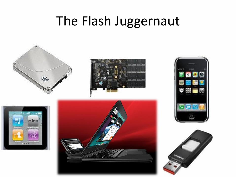
The Flash Juggernaut

Flash is Fast!
Lat.: 7.1msBW: 2.6MB/s
1x1x
68us250MB/s
104x96x
• Random 4KB Reads from user space
Hard Drives PCIe-Flash2007

Flash Operations
Erase
Read
Flo
atin
g G
ate
Program
20V
0V
0V
5V
0V
1V
20V0V

Organizing Flash Cells into Chips

Organizing Flash Cells into Chips
• ~16K blocks/chip
• ~16-64Gbits/chip

Flash Operations
… …
Block 0
Block 1
Block 2
Block n
…
Page: 0 1 2 3 4 nn-1n-2n-3n-4
…
…
…
…
Erase Blocks
ProgramPages
SLC: Single Level Cell
MLC: Multi Level Cell
== 1 bit
== 2 bits
TLC: Triple Level Cell
== 3 bits

Single-Level Cell
== 1 bit
Endurance: 100,000 CyclesData retention: 10 yearsRead Latency: 25usProgram Latency: 100-200us

Multi-Level Cell (2 bits)
== 2 bits
Endurance: 5000-10,000 CyclesData retention: 3-10 yearsRead Latency: 25-37usProgram Latency: 600-1800us

Triple-level Cell (3bits)
== 3 bits
Endurance: ~500-1000 CyclesData retention: 3 yearsRead Time: 60-120usProgram Time: 500-6500us

3D Nand
• SLC, MLC, and TLC NAND cells are 4F2 devices.– 1.33 – 4F2 per bit
• Higher densities require 3D designs– Samsung has demonstrated
24 layers
– 2-4x density boost
• http://bcove.me/xz2o1af5
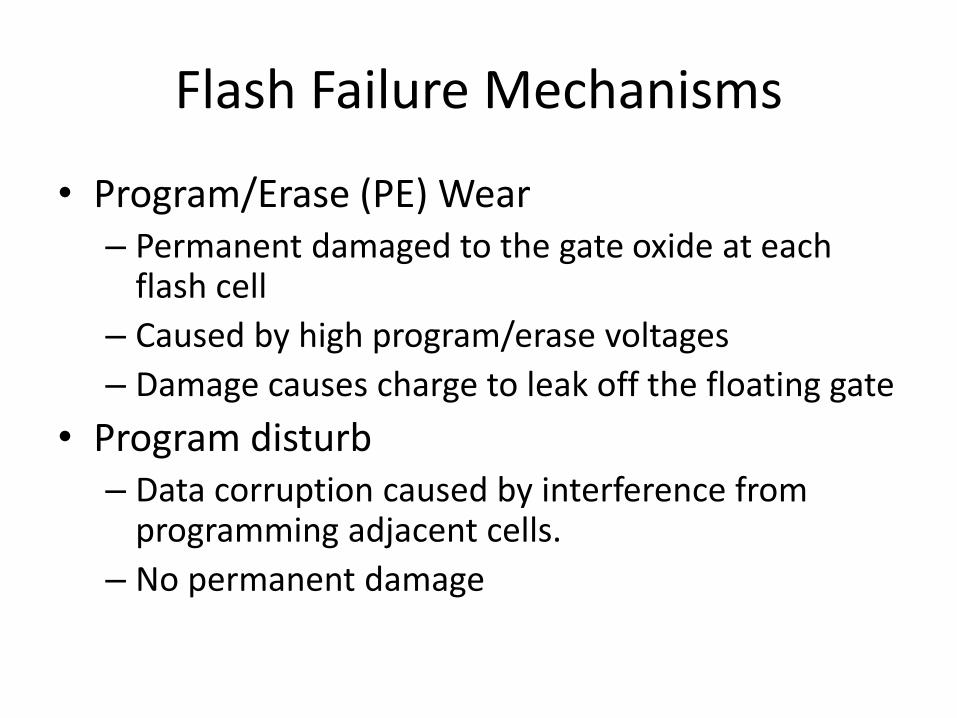
Flash Failure Mechanisms
• Program/Erase (PE) Wear– Permanent damaged to the gate oxide at each
flash cell
– Caused by high program/erase voltages
– Damage causes charge to leak off the floating gate
• Program disturb– Data corruption caused by interference from
programming adjacent cells.
– No permanent damage
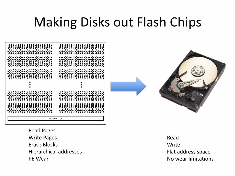
Making Disks out Flash Chips
Read PagesWrite PagesErase BlocksHierarchical addressesPE Wear
ReadWriteFlat address spaceNo wear limitations
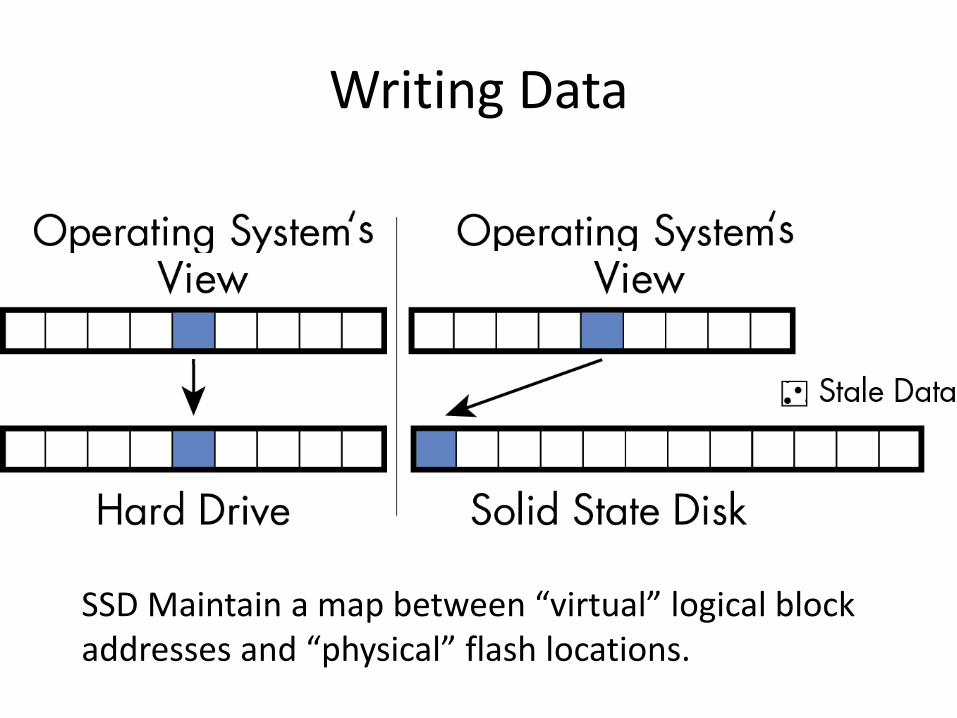
Writing Data
SSD Maintain a map between “virtual” logical block addresses and “physical” flash locations.

Writing more data…
When you overwrite data, it goes to a new location.

Flash Translation Layer (FTL)
User
• Logical Block Address
Flash
• Write pages in order
• Erase/Write granularity
• Wears out
FTL
• Logical Physical map
• Wear leveling
• Power cycle recovery
Software
FTL
Flash
101001011010001
010100100101011
101010110101001
111111111111111
111111111111111
111111111111111
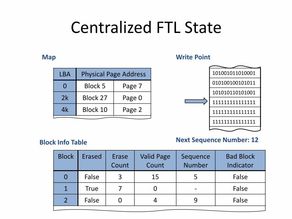
Centralized FTL State
Write PointMap
Block Info Table
LBA Physical Page Address
0 Block 5 Page 7
2k Block 27 Page 0
4k Block 10 Page 2
Block Erased Erase Count
Valid Page Count
Sequence Number
Bad Block Indicator
0 False 3 15 5 False
1 True 7 0 - False
2 False 0 4 9 False
Next Sequence Number: 12

Read
2. Map
LBA Physical Page Address
0 Block 5 Page 7
2k Block 27 Page 0
4k Block 10 Page 2
Software
FTL
Flash
1. Read Data at LBA 2k
3. Flash Operation