finitedifferencetimedomainmodelingof ... · 302 d’orazio et al. high efficiency input and...
TRANSCRIPT
Progress In Electromagnetics Research, PIER 39, 299–339, 2003
FINITE DIFFERENCE TIME DOMAIN MODELING OFLIGHT AMPLIFICATION IN ACTIVE PHOTONICBAND GAP STRUCTURES
A. D’Orazio, V. De Palo, M. De Sario, V. Petruzzelliand F. Prudenzano
Dipartimento di Elettrotecnica ed ElettronicaPolitecnico di BariVia Re David, 200-70125 Bari, Italy
Abstract—The paper deals with the modeling, based on theFinite Difference Time Domain method, of active one- and two-dimensional photonic crystals. The onset of laser oscillation isobserved by simulating the active substance as having a negativefrequency-dependent Lorentzian-shaped conductivity so including intoMaxwell’s equations an electric current density. Particular attentionis devoted to the implementation of uniaxial perfectly matchedlayer absorbing boundary conditions for the simulation of infinitelyextending structures having gain features. Laser behaviour is simulatedas a function of various parameters; the threshold wavelength andconductivity are evaluated as the wavelength and conductivity wherethe transmittance diverges. Moreover, the properties of the activetwo-dimensional photonic band gap structures are given in terms ofa Q quality factor which increases by increasing the crystal size andstrongly depends on the lattice shape. For the square lattice, when thecrystal size increases from N = 2 to N = 8 the Q-factor increases byabout an order of magnitude (from 0.027 to 0.110) for TE polarizationwhile for TM polarization it decreases from 0.025 to 0.022. At lastthe Q-factor pertaining to the chess-board lattice, to parity of otherparameters, assumes greater values and already for N = 4, it reachesthe values obtained for the 16× 8 square lattice, for both TE and TMpolarizations.

300 D’Orazio et al.
1 Introduction
2 FDTD Modeling of PBG Structures with LorentzianGain Media
3 1D PBG Structure Simulation Results
4 2D PBG Structure Numerical Results
5 Conclusion
Appendix A. 2D FDTD Algorithm for Active Materials
Appendix B. PML Termination for Conductive DispersiveMedia
References
1. INTRODUCTION
Electromagnetism is the fundamental mediator of all interactions inatomic physics and condensed matter physics, in other words, theforce that governs the structure of ordinary matter. In a novel class ofengineered dielectric materials, known as photonic crystals (PhCs) orPhotonic Band Gap (PBG) materials, new electromagnetic effects canbe obtained [1–4]. The light localization is a particular interestingphenomenon of fundamental importance for using optical waves ininformation and communication technologies. Because of the periodicspatial modulation of the dielectric constant, the dispersion equation ofthe electromagnetic eigenmodes in photonic crystals are quite differentfrom those in uniform materials. A part from the formation ofpass bands and band gaps of eigenfrequencies, extremely small groupvelocity (the derivative of the angular frequency ω of the radiation fieldwith respect to the wave vector k,vg = dω/dk) can be easily obtainedin a photonic crystal. In fact a large enhancement of light amplificationis obtained when vg is small, the amplitude amplification factor beingproportional to v−1
g [5].By considering the photonic band structure, given by the
normalized frequency ωn = ωa/2πc as a function of the wave vector k(a and c being the lattice constant and the light velocity in the vacuo,respectively) of a one-dimensional (1D), or two-dimensional (2D) orthree-dimensional (3D) lattice, it is possible to find that there existpoints, exactly the band gap edges, where vg is equal to zero. Moreover,the photonic band structure of a 2D or a 3D PhC shows wholefrequency ranges in the Brillouin zone characterized by a small groupvelocity. This phenomenon, known as the group velocity anomaly,
Finite difference time domain modeling 301
is peculiar to 2D and 3D photonic crystals and it does not occur in1D periodic structures. The enhancement of light amplification dueto a small group velocity can be so explained [6]: since the photonundergoes many multiple reflections at the lattice discontinuities, theoptical path length increases and the photon spends a long time in thelattice moving at a mean velocity equal to vg. In presence of an activemedium, the increase of the interaction time between radiation fieldand matter gives rise to the enhancement of gain.
A subsequent effect of these phenomena is the laser oscillationonset which can be obtained in any type of PhC, not depending onthe geometrical complexity of the lattice. In particular, Ohtaka [7]verified that the onset of the laser oscillation is due to the presence ofdivergent peaks in the transmission spectrum. In the case of 1D PhCs,this phenomenon occurs when high gain materials and an opportunenumber N of lattice periods are involved, while lower N (even N = 1)and drastically reduced threshold gain values are required in 2D and3D PhCs in order to obtain the same laser action. On the other hand,it was shown that the 1D PBG lattices exhibit nearly the same lasingproperties aside from the band location in the frequency spectrum.This is in clear contrast to the lasing action in 2D or 3D photoniccrystals, where the onset of the lasing in higher bands is much easierthan in the first band.
A number of prototypal “active” devices based on photoniccrystals were designed, constructed and tested [8–16]. As an example,Inoue et al. [17] reported the observation of lasing action in a 2Dphotonic lattice. By optically pumping a dye-solution filled in air-holesof the 2D lattice, laser action without external mirrors is found to occurat a specific wavelength corresponding to a flat band-dispersion in high-symmetry direction of the 2D lattice plane, the small group velocitybeing responsible for the lasing. Further increasing the pump-fluence,another laser action is found to occur around a peak wavelength of thespontaneous emission spectrum.
Moreover, strong feedback and memory effects accompanycollective light emission near the photonic band edge. Near a true3D photonic band edge, this leads to lasing without a conventionaloptical cavity. A precursor of this effect was found in the 2D band edgemicro-laser [18] in which lasing from electrically injected electron-holepairs in a multiple quantum well array occurs preferentially at the 2Dphotonic band edge, even though the emission from the active regionexhibits a broad frequency distribution.
The active PhC technology offers significant promises in this arenabut, before this can become a true reality, a number of technologicalbarriers, as repeatable and high-fidelity technologic processes,

302 D’Orazio et al.
high efficiency input and output-coupling devices, manufacturingintegration methods, and so on must to be overcome. Apparently,the engineering perspective of PhC devices requires development ofreliable design tools. As it is well known, the first theories of PhCs werebased on the solid-state physics and band-theory for semiconductormaterials. Due to the vector nature of electromagnetic (e.m.) fields,these early analyses proved their inaccuracy so mathematical tools,incorporating the vector nature of e.m. fields, have been developed. Alargely used technique, which gives results with good agreement withthe experimental ones, is the Plane Wave Method (PWM) where aninfinite period lattice is assumed. This method is no longer valid whena linear defect or a point defect is included in the lattice or when afinite period lattice is considered. For this reason, alternative toolshave been developed: one of the more common is the finite-differencetime-domain (FDTD) method [19].
Till now, active PhC device modeling has been performed inthe frequency domain by assuming the polarizability of the impurityatoms of the gain material independent of angular frequency ω andthe impurities uniformly distributed in the dielectric material: in thiscase the gain material can be modeled by simply assuming a complexdielectric constant (with a negative imaginary part which incorporatesthe population inversion phenomena, the field time dependence beingexp(−jωt). As an example, this formalism was used in [7] to describethe light amplification in active two-dimensional photonic crystals.In this paper, we describe a FDTD formulation that allows themodelling of PBG structures having frequency-dependent optical gainmedia. The frequency dependent gain is incorporated into the electriccurrent density term in Maxwell’s equations by means of a Lorentzianfrequency-dependent negative conductivity. To our knowledge, this isthe first study performed on active PhC devices by means of FDTD.
The paper is organized as it follows. Sect. 2 briefly resumesthe principles of the FDTD method, referring the Reader to theAppendices A and B for more deepening. In particular, Appendix Adescribes the fundamentals of FDTD operation in the case of 2Dphotonic crystals when the frequency dependent gain is incorporatedinto the electric current density term in Maxwell’s equations;Appendix B models the uniaxial perfectly matched layer (UPML)absorbing boundary conditions in presence of infinitely extendingactive media. The reduction of the developed equations for the 1Dperiodic structures can be easily obtained from those obtained for 2Dones while the extension to the 3D periodic structures requires a light,even if tedious, algebraic loading. Sect. 3 of the paper reports theresults of the simulations performed on active 1D photonic crystals.

Finite difference time domain modeling 303
In particular, the light amplification spectra are numerically evaluatedand the lasing threshold conditions are identified by examining thedivergence of transmission and reflection coefficients. Lastly, in Section4 we discuss the strength of the FDTD-based numerical code devoted tothe analysis of active 2D photonic crystals. In particular, the effect ofthe lattice shape on the amplification and transmission characteristicsis evaluated.
2. FDTD MODELING OF PBG STRUCTURES WITHLORENTZIAN GAIN MEDIA
In this section we briefly describe the home-made FDTD algorithmthat allows us the modeling of the active PBG structures. The processof light emission in active PhCs is analogous to the lasing oscillationin distributed feedback lasers: the onset of lasing is equivalent tothe divergence of the transmittance and/or the reflectance of theassumed specimen, as demonstrated by Yariv [20]. Because we areinterested in the evaluation of the lasing threshold conditions, we willdisregard in what follows the nature of the active substance and wewill simply assume that the optical impurities (atoms or molecules)are uniformly distributed in the photonic crystal and their populationinversion is attained by appropriate means such as optical pumping.Under these same hypothesis, several authors [7, 21] modeled theactive substance in the frequency domain by a complex frequency-independent dielectric constant with a negative imaginary part. In ouranalysis developed in the time domain, we consider active structurescomposed by frequency-dependent optical gain media. The frequencydependent gain is incorporated into the electric current density termin Maxwell’s equations by means of a Lorentzian frequency-dependentnegative isotropic conductivity given by:
σ(ω) =Jx(ω)Ex(ω)
=Jy(ω)Ey(ω)
=Jz(ω)Ez(ω)
=1
1 + I/Is
(σ0/2
1 + j(ω − ω0)T2+
σ0/21 + j(ω + ω0)T2
)(1)
where σ0 is the conductivity peak value, linked to the peak value ofthe gain set by the pumping level and the corresponding populationinversion; ω0 is the frequency pertaining to the peak value of theconductivity; T2 is a time constant that defines the spreading of theLorentzian spectral profile, S = (1+I/Is)−1 is the saturation coefficientwhile Is is the saturation intensity. In Eq. (1), the Hermitian symmetryis used for the Lorentzian profile.
304 D’Orazio et al.
The idea of using negative conductivity to describe gain mediahas been inspired by the work in the microwave community wherepositive conductivity is used to simulate the lossy media. So, if positiveconductivity can be used to simulate the attenuation aspects of adispersive medium, then a negative conductivity might be useful forsimulating a medium with gain. The choice of Lorentzian shape forthe conductivity is based on the consideration that more complicatedand, overall, experimental gain spectra can be approximated usinga linear combination of Lorentzians. Another assumption is implicitin disregarding the nature of the active substance: no interactionbetween the input signal and other fields (such as the optical pump)is considered.
The FDTD method is formulated using a central differencediscretization of Maxwell’s curl equations in both time and space(see Appendix A). Yee’s original algorithm and formalism solvingMaxwell’s equations in two dimensions is adopted. The field valueson the nodal points of the discretized finite volume are calculatedin a leapfrog fashion. Due to the use of centered differences in theapproximations, the error is of second order in both the space (∆x,∆z)and time (∆t) steps. In the calculations, the maximum time step thatmay be used is limited by the stability restriction of the finite differenceequations.
The excitation plane needs to be treated carefully when settingup the problem. If a Gaussian source is used as the excitation source,its smooth Gaussian shaped spectrum can provide information fromdc to the desired frequency simply by adjusting the width of the pulse.Therefore, in the following simulations a Gaussian pulse PG is assignedto specific electric or magnetic field components in the FDTD spacelattice at the grid source point (iS , jS , kS):
PG = exp(−(n− no)/nd)2 (2)
This pulse is centered at time step no, exhibits a 1/e characteristicdecay of nd time steps and it has a nonzero value at n = 0.
The successful implementation of the FDTD algorithm isconditioned by the inclusion of accurate and efficient absorbingboundary conditions to emulate electromagnetic interaction in anunbounded space. The perfectly matched layer (PML) absorbingmedium is the ideal candidate for the grid termination, but itsdefinition have to be modified when the computational volume istotally filled with active medium (see Appendix B). In particular, inthe developed code, the UPML are adopted: the conductivity profilefor each side (i = x, y, z) of the grid is defined as:
σPML(i) = σmgNPML (3)

Finite difference time domain modeling 305
withσm = [lnR(0) ln g)/(2ηε∆i(gNPML − 1)]
where η is the vacuum characteristic impedance, NPML is the cellnumber which gives the UPML thickness, g is the geometric scalingof PML conductivity profile, R(0) is the reflection error for normalincidence and ∆i is the spatial step size.
FDTD algorithm allows for obtaining the reflection andtransmission coefficients over a wide band of frequencies in one run. Inour analysis the electromagnetic performance of the PBG structure isdescribed by means of transmission (transmittance T ) and reflection(reflectance R) coefficients, defined in terms of the total time-averagedPoynting’s vector through the input (z = 0) and output (z = L)sections:
T =Pt(z = L)Pi(z = 0)
R =Pr(z = φ)Pi(z = 0)
where
Pi = −12Re
∫width
Eii,ω(x, z = 0)H∗ii,ω(x, z = 0)dx
Pr = −12Re
∫width
Eri,ω(x, z = 0)H∗rj,ω(x, z = 0)dx
Pt = −12Re
∫width
Eti,ω(x, z = L)H∗tj,ω(x, z = L)dx
and Eii,ω and Hij,ω represent, in the frequency domain, the incidentelectric and magnetic field components, obtained numerically anti-transforming Eqs. (A3) and (A4) of Appendix A. Moreover thesubscripts i and j indicate the components Eiy,ω and Hix,ω (Eix,ω andHiy,ω) for TE (TM) polarization. The symbol (∗) indicates the complexconjugate while the integral is extended to the transversal width of thePBG structure along the x direction. The same symbolism is valid forthe reflected and transmitted powers, respectively.
3. 1D PBG STRUCTURE SIMULATION RESULTS
The 1D PBG structure under investigation is shown in Fig. 1. It iscomposed of N layers of active material in air (ε1 = 1); the dielectric

306 D’Orazio et al.
Figure 1. Sketch of one-dimensional PBG stack structure.
constant ε2 of the active layers is assumed equal to 2.0 throughout thepaper, this value being typical for transparent organic polymers. Thelattice constant a = h1 + h2 is put equal to 1µm, and the thicknessh2 of the active thin layer, normalized by a, is taken to be 0.28. Thefrequency ω of light, normalized by 2πc/a, is swept in the frequencyrange of 0 < ωn < 2.0, c being the light velocity in the vacuo. In orderto compare our results with those obtained by other methods [7], thecentral frequency of the examined range corresponds to a frequencyf = 300 THz. We take the xy plane parallel to the layer plane and thez direction in the stack direction.
The FDTD simulations are performed by exciting the PBGstructure with a single-cycle Gaussian pulse centered at time stepno = 100, having nd = 30: for these values the pulse bandwidthcovers the frequency region of interest. The incident field is evaluatedin time domain at the total field/scattered field interface, placed inz = 0. The source plane (z = −zi) is located to a distance from thisdiscontinuity equal to 140 ∆z, that allows the complete evolution andthe return to zero of the Gaussian pulse, before the reflected wavefrom the first layer comes back to the source. The reflected field isevaluated in time domain near the section z = 0 in the scattered fieldregion; the transmitted field is calculated in time at the point z = L,just beyond the end of the PBG structure. The resulting fields areFFT transformed to obtain the frequency spectra.

Finite difference time domain modeling 307
Figure 2. Transmission coefficient T evaluated by means of theFDTD-based code, for the passive PBG structure constituted byN = 8periods of dielectric medium (ε2 = 2.0) and air; lattice constanta = 1µm; thickness of the dielectric thin films h2, normalized by a,equal to 0.28.
The UPML conductivity profile for each side (i = x, y, z) of thegrid is characterized by the following parameters: thickness equalto NPML = 10 cells, geometric scaling of PML conductivity profileg = 2.5, reflection error for normal incidence R(0) = exp(−16) and∆i equal to the spatial step size. The FDTD computational window isidentified by a lattice pitch ∆z = λ/500 = 2 nm in space with λ = 1µmcorresponding to the central frequency of the examined range, and∆t = ∆z/c = 6.66 10−3 fs. These values of the computational domainsteps guarantee good numerical dispersion and stability [4].
We start our simulations by analyzing the periodic passive stackconstituted by N = 8 periods of dielectric layers having ε2 = 2.0 andε1 = 1 (air). Fig. 2 shows the evaluated transmission coefficient ofthe N = 8 period passive stack. The transmission spectrum showsfour band gaps, three of them well defined and centered at the ωnnormalized frequency values equal to 0.44, 0.9 and 1.76 respectively,while the band gap centered at ωn = 1.35 is just hinted reachingonly the value of T = 0.7. These results are in good agreementwith those calculated by using a computer code based on the transfer-

308 D’Orazio et al.
Figure 3. Band structure, obtained by a TMM-based code, of theinfinite PBG stack lattice of dielectric material in air. Other data asthose in Fig. 2.
matrix (TMM) approach [22]†. In particular, Fig. 3 shows the bandstructure, evaluated by TMM, for the wave vector (0, 0, kz) of the x, yaxis infinite periodic stack, by disregarding the active nature of thedielectric substance (kz, of course, is the wave vector component inthe stack direction). In the analyzed range of normalized frequency, wenotice four band gaps, the not shaded spectral ranges representing theband gaps. The first band gap is located in the range of normalizedfrequency 0.4 < ωn < 0.5, while the following band gaps are in theranges 0.86 < ωn < 0.96; 1.34 < ωn < 1.36 and 1.72 < ωn < 1.80, forkz ranging from 0 to 0.5.
Now we consider the active nature of the PBG structure bymodeling the active medium 2 by means of a frequency-dependentnegative conductivity having a Lorentzian gain profile. Moreover,throughout the paper, we will disregard the saturation effects becausethe number of time steps does not allow the structure saturation. Ouranalysis starts by considering a Lorentzian material with an increasingspectral gain profile, characterized by the following parameters:normalized frequency ωn = 2 (corresponding to a wavelength λ0 =0.5µm), σ0 = −3337 S/m, T2 = 0.7 fs. Fig. 4 shows the corresponding† The program “Translight” can be downloaded from http://www.elec.gla.uk/˜areynolds/software.html. It is based on the paper by Bell et al. [22]

Finite difference time domain modeling 309
Figure 4. Transmission coefficient of the N = 8 period activestack; active Lorentzian material characterized by a conductivity σ(ω)having the following parameters: ωn = 2 (λ0 = 0.5µm), σ0 =−3337 S/m, T2 = 0.7 fs, the modulus and phase of σ(ω) are herereported, too. Other data as those in Fig. 2.
modulus (dashed line) and phase (dashed-dotted line) of the abovedefined conductivity σ(ωn) and the evaluated transmission coefficientT , obtained by our FDTD-based code, for the PBG active stackconstituted by N = 8 layers of active material. The transmissioncoefficient, of course, is higher than that shown in Fig. 2 for the passivePBG structure: the T peak values increase by increasing the frequency,according to the shape of the conductivity modulus, reaching themaximum value T = 7.5 in correspondence of the fourth band gap.Moreover, the T peaks are localized at the inferior edge of the bandgaps. This is due to the fact that the dielectric constant ε2 of the gainlayer is greater than that ε1 of the passive layer; while if we assumeε2 < ε1, then we calculate that the maximum T peak values occurat the superior edge of the photonic band gaps, to a parity of otherparameters.
Now a Lorentzian material with a decreasing spectral gain profile,characterized by the following parameters: normalized frequency ωn =1 (corresponding to λ0 = 1µm), σ0 = −1668 S/m, T2 = 0.07 fs,is investigated. Even in this example, the evaluated transmissioncoefficient for the N = 8 period active stack, depicted in Fig. 5, shows,also now, peaks localized at the inferior edge of each band gap but theyexhibit decreasing values by increasing the frequency. For a greater

310 D’Orazio et al.
Figure 5. Transmission coefficient of the N = 8 period PBG structurehaving the active Lorentzian material characterized by a conductivityσ(ω) with the following parameters: ωn = 1 (λ0 = 1µm), σ0 =−1668 S/m, T2 = 0.07 fs.
Figure 6. Transmission coefficient of the N = 8 period active stack,the active Lorentzian material being characterized by the conductivityσ(ω) having the same numerical values as in Fig. 5 but a greater timeconstant T2 = 0.07 ps (narrower frequency range).

Finite difference time domain modeling 311
Figure 7. Transmission coefficient of the N = 8 period active stackhaving the active Lorentzian material characterized by the followingparameters: ωn = 1.71 (λ0 = 0.58µm), σ = −2853 S/m, T2 = 0.07 ps;i.e., centered at the inferior edge of the fourth band gap.
time constant T2, the Lorentzian spectral gain profile is concentrated ina narrow frequency range so, as we can infer from Fig. 6 (ωn = 1, σ0 =−1668 S/m, T2 = 0.07 ps), the corresponding transmission spectrumshows a peak value well localized at the frequency value ωn = 1 whichcorresponds to the maximum value of the conductivity and, of course,it is characterized by the same T values pertaining to the passive stackout of the very narrow frequency range centered at ωn = 1.
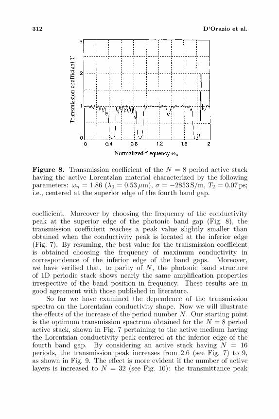
A sensible enhancement of the peak value of the transmissioncoefficient T is obtained by fixing the frequency of maximumconductivity just in correspondence of an edge frequency of a bandgap. As an example, by considering the Lorentzian conductivity profile(σ0 = −2853 S/m, T2 = 0.07 ps) having the maximum value fixed atthe inferior edge of the fourth band gap ωn = 1.71 (λ0 = 0.58µm), weobtain the transmission coefficient plot shown in Fig. 7 which exhibitsa good peak just at ωn = 1.71. Of course, if we center the Lorentzianat the superior edge ωn = 1.86 (λ0 = 0.53µm) of the same fourth bandgap, we obtain the spectrum of Fig. 8 where the peak at ωn = 1.86 isapparent.
By comparing these spectra, we infer that the shift of theconductivity peak value into correspondence of an edge of a band gapinduces a sensible enhancement of the peak value of the transmission
312 D’Orazio et al.
Figure 8. Transmission coefficient of the N = 8 period active stackhaving the active Lorentzian material characterized by the followingparameters: ωn = 1.86 (λ0 = 0.53µm), σ = −2853 S/m, T2 = 0.07 ps;i.e., centered at the superior edge of the fourth band gap.
coefficient. Moreover by choosing the frequency of the conductivitypeak at the superior edge of the photonic band gap (Fig. 8), thetransmission coefficient reaches a peak value slightly smaller thanobtained when the conductivity peak is located at the inferior edge(Fig. 7). By resuming, the best value for the transmission coefficientis obtained choosing the frequency of maximum conductivity incorrespondence of the inferior edge of the band gaps. Moreover,we have verified that, to parity of N , the photonic band structureof 1D periodic stack shows nearly the same amplification propertiesirrespective of the band position in frequency. These results are ingood agreement with those published in literature.
So far we have examined the dependence of the transmissionspectra on the Lorentzian conductivity shape. Now we will illustratethe effects of the increase of the period number N . Our starting pointis the optimum transmission spectrum obtained for the N = 8 periodactive stack, shown in Fig. 7 pertaining to the active medium havingthe Lorentzian conductivity peak centered at the inferior edge of thefourth band gap. By considering an active stack having N = 16periods, the transmission peak increases from 2.6 (see Fig. 7) to 9,as shown in Fig. 9. The effect is more evident if the number of activelayers is increased to N = 32 (see Fig. 10): the transmittance peak

Finite difference time domain modeling 313
Figure 9. Transmission coefficient of the N = 16 period active stack;other data as those in Fig. 7.
Figure 10. Transmittance of the N = 32 period active PBG structurehaving an active Lorentzian material characterized by the followingparameters: ωn = 1.71, σ0 = −2853 S/m, T2 = 0.07 ps.

314 D’Orazio et al.
Figure 11. Transmission and reflection coefficients of the N = 32period active stack, obtained by the TMM-based code, by modelingthe active layer by a the complex dielectric constant ε = 2.0− j0.01.
reaches about 34 dB. The divergence of the T coefficient is indicativeof the onset of the laser oscillation as we will see in Fig. 13. On theother hands, the stack having N = 8 periods is characterized by athreshold conductivity value, which gives rise to a T singularity equalto about 32 dB, σ0 = −19971 S/m, value seven times greater than thatconsidered for the 32-period active stack (σ0 = −2853 S/m).
To definitively validate the effectiveness of the developed FDTD-based code, the same structure has been simulated by the TMM-basedcode. Acting the TMM in the frequency domain, the properties of theactive material have been incorporated into the negative imaginarypart ε′′ of the dielectric constant of the active layers ε2 = ε′ + jε′′,with ε′ = 2.0. The population inversion has been taken into accountinto the negative imaginary part ε′′. The results obtained for the caseN = 32 period active stack layers with ε2 = 2.0− j0.01 (time operatore−jωt), are shown in Fig. 11.
In the FDTD algorithm, we have then introduced the electriccurrent density expressed by means of an equivalent negativeconductivity given by σeq = ωε0ε
′′. Of course this model is exactonly at the frequency that defines the equivalent conductivity; for thisreason the analysis is applied to the third band gap that is narrowerthan the others. The transmission and reflection coefficients for a stackconsisting of N = 32 layers of active material having σeq = 223.4 S/m

Finite difference time domain modeling 315
Figure 12. Transmission and reflection coefficients of the N = 32period active stack, obtained by the FDTD-based code by assumingin Maxwell’s propagator an equivalent conductivity σeq = ωε0ε
′′ =223.4 S/m, ωn = 1.34.
at the normalized frequency ωn = 1.34, corresponding to ε′′ = 0.01are shown in Fig. 12. At the normalized frequency value ωn = 1.34,where the σeq has been evaluated, the results obtained by meansof both methods are in good agreement, within the bounds of thedifferent computation resolution. In fact the FDTD code accounts 480samples in the examined range of normalized frequency while the TMMsimulation accounts 9999 samples in the same normalized frequencyrange.
The lasing oscillation, observed by the FDTD simulator, isdepicted in Fig. 13 which shows the evaluated time evolution of theelectric field Ey in the output section of the 32-period Lorentzian(λ0 = 0.58µm, σ0 = −2853 S/m, T2 = 0.07 ps) active stack. For thesedata, the T coefficient exhibits a divergent peak at the lower edge ofthe fourth band gap and all the electric and magnetic field componentamplitudes, but overall the Ey component, increase in time. The fieldcomponent Ey tends to level off to a sinusoidal steady-state oscillationat the frequency that defines the maximum of the conductivity. This isapparent in Fig. 13 where the final time steps are plotted in expandedtime scale.

316 D’Orazio et al.
Figure 13. FDTD-computed time evolution of the electric fieldcomponent Ey in the output section for the case N = 32, ωn =1.71 (λ0 = 0.58µm), σ0 = −2853 S/m, T2 = 0.07 ps.
4. 2D PBG STRUCTURE NUMERICAL RESULTS
The 2D PBG structure, under investigation, consists of M columns ofactive material in air, located along the x direction and N columnsalong the propagation direction z, the infinitely long column axis lyingalong the y-axis. The relative dielectric constant ε2 of the active layersis assumed equal to 2.0 throughout the paper. The columns have asquare cross-section and are arranged in a square lattice (see Fig. 14a)having lattice constant a, equal to 1µm. The square column side d,normalized by a, is taken equal to 0.53. The light normalized frequencyωn is assumed in the frequency range of 0 < ωn < 2.0.
The band structures for the corresponding M = N = ∞ passive2D photonic crystal, evaluated for TE and TM polarizations, showtotal band gaps in the ranges of normalized frequency 0.44 < ωn < 0.56and 0.82 < ωn < 0.9, for the wave vector component kz ranging from0 to 0.5. For the considered lattice, the TE polarization accounts forthe Ey, Hx and Hz field components, while the TM polarization ischaracterized by the Hy, Ex and Ez field components.
To evaluate the spectral characteristics of the 2D PBG structures,the proprietary FDTD simulator has been used under the following

Finite difference time domain modeling 317
(a)
(b)
Figure 14. Cross section of the elementary cell of a two-dimensionalPBG structure characterized by: (a) a square lattice and (b) a chess-board lattice.
conditions. The 2D PBG structure is excited with a single-cycleGaussian pulse (no = 50, nd = 5), located to a distance from thefirst discontinuity equal to zi = a/2 = 500 nm. The FDTD gridaccounts space steps equal to ∆x = ∆z = λc/25 = 40 nm, and timestep ∆t = ∆z/(c ·
√2) = 9.42 10−2 fs. The UPML parameter values
are the same assumed in Sect. 3.The first aim of this investigation consists of illustrating the

318 D’Orazio et al.
influence of a finite number of periods N along the z direction onthe spectral characteristics, having fixed M = 16 columns along the xaxis. For this reason, a square lattice of M ×N = 16 × 2 columns ofdielectric passive material (ε2 = 2.0) in air is at first considered. Fig. 15shows the FDTD evaluated transmission T and reflection R coefficientsfor: (a) TE and (b) TM polarizations. These results resemble theones evaluated for the infinite passive square lattice; in fact a welldefined photonic band gap is observable for a normalized frequency ofωn = 0.9 in the case of TE polarization while the transmission dipof TM polarization reaches only the value of 0.5. Moreover the firstband gap near the normalized frequency ωn = 0.4, visible in the bandstructure of the infinite passive PBG structure, is not so pronounced,showing the strong influence of the limited number of M ×N columnsof the investigated lattice with respect to the case of M = N =∞.
We consider now the corresponding active PBG structures: ofcourse the transmittance and reflectance significantly change. Sincethe spectral characteristics depend on the polarization, throughoutall the paper, the results will be illustrated for both TE and TMpolarizations. We start our simulations by considering a Lorentzianactive material with a spectral gain profile centered in correspondenceof the inferior edge of the second photonic band gap, identifiedby the following parameters: normalized frequency ωn = 0.82(corresponding to conductivity peak wavelength value λ0 = 1.22µm),σ0 = −13685 S/m, T2 = 0.07 ps. Fig. 16 depicts the TE andTM evaluated transmission and reflection coefficients for the 16 × 2active 2D lattice. As expected, the peak value of the transmissioncoefficient is localized in correspondence of the frequency ωn = 0.82that identifies the conductivity maximum value and it reaches the valueof about 3.38 for TE polarization and 1.92 for the TM one. Thesespectra show that the square lattice exhibits better performance forTE polarization. Moreover, it is interesting to outline that even thereflection coefficient spectrum for TE-polarization exhibits a peak justat the normalized frequency value corresponding to the conductivitypeak: this occurrence will assume a significant role in the onset of thelasing oscillation.
Let us consider now the effect on the transmission andreflection coefficients of the active period number increasing along thepropagation direction, to parity of the other data and, in particular, ofconductivity Lorentzian shape. In the case of a 16×4 active lattice, theT peak remarkably increases, reaching the value of about 39 and 4.7 forTE and TM polarization, respectively. The reflection coefficient R forTE polarization increases till to 104 while for TM polarization the Rpeak is only 0.7. The examined structure gives rise to the stimulated

Finite difference time domain modeling 319
(a)
(b)
Figure 15. Transmission and reflection coefficients for the squarelattice of 16 × 2 columns of dielectric passive materials (ε2 = 2.0) inair: (a) TE polarization, (b) TM polarization.

320 D’Orazio et al.
(a)
(b)
Figure 16. Transmission and reflection coefficients of the active 16×2square lattice. The active Lorentzian material is characterized by thefollowing parameters: ωn = 0.82, σ0 = −13685 S/m, T2 = 0.07 ps: (a)TE polarization, (b) TM polarization.

Finite difference time domain modeling 321
emission phenomenon as we can infer from Fig. 17 where the timeevolution of the electric field component Ey at the output section z = Lis depicted: a sinusoidal oscillation just at the frequency ωn = 0.82,that defines the maximum of the conductivity, is apparent: however itsnormalized amplitude reaches only the maximum value equal to 0.2.We notice that the field is well confined in the active columns which aredenser than the air. This occurrence is more evident in Fig. 17b whichshows the magnified plot of the Ey evolution in the output section,restricted to a small range of time steps.
More interesting effects are observable when the number ofperiods along the z direction is increased. Fig. 18 shows the sum oftransmittance and the reflectance for a TE polarized wave propagatingin a 16 × N lattice with N = 2 (dashed-dotted line), N = 4 (dashedline), N = 8 (solid line). For N = 2 and 4 the sum is equal toabout the unity (like for a lossless or a gain less material) in the wholeexamined spectral large except in correspondence of the inferior edge ofthe band gap where we superimposed the conductivity peak and a largeenhancement, due to the stimulated emission, is apparent. By furtherincreasing the number of the active lattice periods to N = 8 the sumof transmittance and reflectance assumes a value equal to 30 dB in asmall range of low normalized frequencies near the origin, it settles in avalue a bit lower than 103 dB in the whole spectral range and the peakat the band edge reaches a noticeable large value, the enhancementfactor being four orders of magnitude greater. This effect seems tobe a phenomenon of saturation due to the high value of the assumedconductivity peak. In fact, in this case the transmission and reflectionspectra do not exhibit the usual band structure and, therefore, theperiodic lattice behaves as a bulk active medium. In the case of TMpolarization, the sum of transmittance and reflectance exhibits a moreregular shape well settled equal to unit in the whole spectral range withthe peak fixed in correspondence of the conductivity peak, for all theconsidered N values. The peak value, obtained for the N = 8 periodlattice along the z direction reaches 200 dB. The effect of saturationfor this type of polarization does not turn up.
Fig. 19 illustrates the time evolution of the TE-polarized fieldcomponent Ey at the output section z = L of the 16× 8 square latticeand other data as those in Fig. 16. By increasing the number of theactive layers along the propagation direction, the normalized amplitudeof the field component increases being two order of magnitude greaterthan the field amplitude evaluated for the 16× 4 lattice. Moreover, alasing oscillation is established just at the frequency that defines themaximum of the conductivity. The maximum amplitude of oscillationis localized in correspondence of the central section along the x-axis.

322 D’Orazio et al.
(a)
(b)
Figure 17. Time evolution of the electric field component Ey at theoutput section of 16×4 active square lattice; (b) expanded time scale ofthe steady-state region showing a single mode oscillation at λ0. Otherdata as those in Fig. 16.

Finite difference time domain modeling 323
Figure 18. Sum of transmittance and reflectance for a TE polarizedwave propagating in a 16 × N square lattice: N = 2 (dashed-dottedline), N = 4 (dashed line), N = 8 (solid line).
Another parameter that influences the characteristics of the PBGstructure is the lattice shape. We now investigate the passive photoniccrystal having a chess-board lattice (see Fig. 16b) characterized bythe presence of a dielectric active column in the center of the crosssection of the square elementary cell. The band structure of the infinitepassive PhC, with respect to the square lattice, is characterized by theabsence of the band gap localized in correspondence of the normalizedfrequency value equal to 0.4 for both polarizations. Moreover the bandgap centered at 0.75 is completely open only for the TE polarization.
As for the square lattice, we consider the PGB structure madeof an optical gain medium having a Lorentzian spectral gain profile,characterized by the following parameters: ωn = 0.82 (λ0 = 1.22µm),σ0 = −13685 S/m, T2 = 0.07 ps. For a 16 × 2 chess-board lattice,the evaluated transmission peak is 76.43 for TE polarization and18.98 for TM polarization, much higher than those evaluated for thesquare lattice: this occurrence is due to the shape of lattice which ischaracterized by a greater filling factor. In the case of the 16×4 chess-board lattice, the transmittance increases till to 26 dB and 8.6 dB forTE and TM polarizations, respectively.

324 D’Orazio et al.
(a)
(b)
Figure 19. (a) Time evolution of the electric field component Eyat the output section of the 16 × 8 period square active lattice; (b)expanded time scale of the steady-state region:a single mode oscillationat λ0 is apparent.

Finite difference time domain modeling 325
Figure 20. Sum of transmittance and reflectance for a TE polarizedwave propagating in a 16×N chess-board lattice: N = 4 (dashed line),N = 8 (solid line), being the active Lorentzian material characterizedby the following parameters: ωn = 1.22µm, σ0 = −1368 S/m, T2 =0.07 ps.
Because we obtain substantially high transmission peak values inthe structure with a low number of periods along the z direction, andto avoid the saturation effects, we consider a Lorentzian conductivityhaving the peak value one order of magnitude lower than that assumedfor the square lattice, σ0 = −1368 S/m, centered in correspondence ofthe inferior edge of the first photonic band gap for TE modes. Fig. 20shows the sum of transmission and reflection coefficients evaluated forthe 16×4 and 16×8 chess-board lattices. The peak of (R+T ) assumesvalues equal to 1.3 and 2, respectively. In this case no saturationeffect is evident but the evaluated T coefficient values are greater thanthose evaluated in the case of the square lattice. Of course, the Tcoefficient values are greater than those evaluated for a 1D structure,to parity of other geometrical and physical parameters, showing thebetter performance of the 2D active lattice.
To conclude, Tab. 1 shows the evaluated Q-factor, defined asQ = ωc/∆ω where ωc is the resonant angular frequency (in our case,practically equal to ω0) and ∆ω is the full-width at half power of the

326 D’Orazio et al.
Table 1. Q-factor for square and chess-board 2D active latticesconsisting of 16×N rods.
N=2 N=4 N=8
Square lattice(σ0=13685 S/m)
TE modes: Q=0.027TM modes: Q=0.025
TE modes: Q=0.038TM modes: Q=0.023
TE modes: Q=0.110TM modes: Q=0.022
Chess-board lattice(σ0=13685 S/m)
TE modes: Q=0.081TM modes: Q=0.055
TE modes: Q=0.126TM modes: Q=0.027
TE modes: Q=1.712TM modes: Q=0.020
transmitted peak, inherent in two different lattice shapes and crystalsizes. For the square lattice, when the crystal size increases from N = 2to N = 8, the Q-factor increases by about an order of magnitude(from 0.027 to 0.110) for TE polarization while for TM polarization itslightly decreases from 0.025 to 0.022. It is interesting to note that theQ-factor for the chess-board lattice, in the same conditions, assumesgreater values and already for N = 4 the Q-factors for both TE andTM polarizations reach the values obtained for the 16×8 square lattice.
5. CONCLUSION
This paper shows the strength of a proprietary FDTD simulator tomodel 1D and 2D active photonic crystals. In particular, the effectson the transmission spectrum due to the introduction into the PBGstructure of Lorentzian gain materials, have been examined. In thecase of 1D active structure an enhancement of the peak value of thetransmission coefficient and the onset of lasing in the PBG active stackare obtained by increasing the number of periods of active stack andby setting the maximum value of the conductivity in correspondenceof the lower edge of a band gap. Moreover the performance of theactive 2D PBG structures depends on the lattice shape and, of course,is better than that of the 1D ones.
APPENDIX A. 2D FDTD ALGORITHM FOR ACTIVEMATERIALS
For self-consistency, we develop here the basic equations of theapplied method, devoted to the analysis of two-dimensional structuresin presence of active media. The frequency dependent gain isincorporated into the electric current density term in Maxwell’sequations by means of a Lorentzian frequency-dependent negative

Finite difference time domain modeling 327
conductivity. To avoid confusion with respect to other alreadypublished papers and books, we exactly follow the notation of Ref.[19] where the guide-lines of the propagation algorithms are discussed.
Two-dimensional (∂/∂y = 0) Maxwell’s equations in rectangularframe coordinates (see Fig. 1), describing the electric and magneticfield components propagating through a nonmagnetic (µ = µ0),isotropic medium, are:
∂Hx
∂t=
1µ0
∂Ey∂z
∂Hy
∂t=
1µ0
[∂Ez∂x− ∂Ex
∂z
]∂Hz
∂t= − 1
µ0
∂Ey∂x
∂Ex∂t
=1ε
[−∂Hy
∂z− Jx
]∂Ey∂t
=1ε
[∂Hx
∂z− ∂Hz
∂x− Jy
]∂Ez∂t
=1ε
[∂Hy
∂x− Jz
]
(A1)
The scalar frequency-dependent conductivity that links theelectric field and the current density is given by [19]:
σ(ω) =Jx(ω)Ex(ω)
=Jy(ω)Ey(ω)
=Jz(ω)Ez(ω)
=1
1 + I/Is
(σ0/2
1 + j(ω − ω0)T2+
σ0/21 + j(ω + ω0)T2
)(A2)
In this expression the Hermitian symmetry is used for the Lorentzianprofile and σ0 is the peak value of the conductivity, linked to thepeak value of the gain set by the pumping level and the resultingpopulation inversion; ω0 is the frequency pertaining to the peak valueof the conductivity; T2 is a time constant which defines the spreadingof the Lorentzian spectral profile, S = (1 + I/Is)−1 is the saturationcoefficient while Is is the saturation intensity. The explicit finite-difference equations for the electric field components are:
En+1x (i, k) = En
x (i, k) +∆t
ε∆z
[Hn+1/2y (i, k−1/2)−Hn+1/2
y (i, k+1/2)]
−∆t
2ε
[Jn+1x (i, k) + Jnx (i, k)
](A3a)

328 D’Orazio et al.
En+1y (i, k) = En
y (i, k) +∆t
ε∆z
[Hn+1/2x (i, k+1/2)−Hn+1/2
x (i, k−1/2)]
− ∆t
ε∆x
[Hn+1/2z (i+ 1/2, k)−Hn+1/2
z (i− 1/2, k)]
−∆t
2ε
[Jn+1y (i, k) + Jny (i, k)
](A3b)
En+1z (i, k) = En
z (i, k) +∆t
ε∆x
[Hn+1/2y (i+1/2, k)−Hn+1/2
y (i−1/2, k)]
−∆t
2ε
[Jn+1z (i, k) + Jnz (i, k)
](A3c)
where:
Jn+1x (i, k) = Jnx (i, k) +
∆t
2
[Fn+1x (i, k) + Fnx (i, k)
]
Jn+1y (i, k) = Jny (i, k) +
∆t
2
[Fn+1y (i, k) + Fny (i, k)
]
Jn+1z (i, k) = Jnz (i, k) +
∆t
2
[Fn+1z (i, k) + Fnz (i, k)
]and
Fn+1x (i, k) = A1x(i, k)
[Hn+1/2y (i, k − 1/2)−Hn+1/2
y (i, k + 1/2)]
+A2x(i, k)Enx (i, k) +A3x(i, k)Jnx (i, k) +A4x(i, k)Fnx (i, k)
A1x(i, k) =4∆tSx(i, k)σ0(∆t+ 2T2)
βx(i, k)∆z
A2x(i, k) =8εSx(i, k)σ0∆t
βx(i, k)
A3x(i, k) = −4∆t[2ε
(1 + ω2
0T22
)+ Sx(i, k)σ0(∆t+ 2T2)
]βx(i, k)
A4x(i, k) = −8εT2(∆t−T2)βx(i, k)
− (∆t)2[2ε(1+ω20T
22 )+Sx(i, k)σ0(∆t+2T2)]βx(i, k)
βx(i, k) = 8εT2(∆t+T2)+(∆t)2[2ε
(1+ω2
0T22
)+Sx(i, k)σ0(∆t+2T2)
]
Sx(i, k) =[1 +
Ix(i, k)Is
]−1
, Ix(i, k) = 0.5cnε0(Epeakx (i, k)
)2
Here Sx is the saturation coefficient that contains feedback informationof the latest peak electric field component Ex. Moreover:

Finite difference time domain modeling 329
Fn+1y (i, k) = A11y(i, k)
[Hn+1/2x (i, k + 1/2)−Hn+1/2
x (i, k − 1/2)]
+A12y(i, k)[Hn+1/2z (i− 1/2, k)−Hn+1/2
z (i+ 1/2, k)]
+A2y(i, k)Eny (i, k) +A3y(i, k)Jny (i, k) +A4y(i, k)Fny (i, k)
where
A11y(i, k) =4∆tSy(i, k)σ0(∆t+ 2T2)
βy(i, k)∆z
A12y(i, k) =4∆tSy(i, k)σ0(∆t+ 2T2)
βy(i, k)∆x
A2y(i, k) =8εSy(i, k)σ0∆t
βy(i, k)
A3y(i, k) = −4∆t[2ε
(1 + ω2
0T22
)+ Sy(i, k)σ0(∆t+ 2T2)
]βy(i, k)
A4y(i, k) = −8εT2(∆t−T2)βy(i, k)
− (∆t)2[2ε(1+ω20T
22 )+Sy(i, k)σ0(∆t+2T2)]βy(i, k)
βy(i, k) = 8εT2(∆t+T2)+(∆t)2[2ε
(1+ω2
0T22
)+Sy(i, k)σ0(∆t+2T2)
]
Sy(i, k) =[1 +
Iy(i, k)Is
]−1
, Iy(i, k) = 0.5cnε0(Epeaky (i, k)
)2
and
Fn+1z = A1z(i, k)
[Hn+1/2y (i+ 1/2, k)−Hn+1/2
y (i− 1/2, k)]
+A2z(i, k)Enz (i, k) +A3z(i, k)Jnz (i, k) +A4z(i, k)Fnz (i, k)
A1z(i, k) =4∆tSz(i, k)σ0(∆t+ 2T2)
βz(i, k)∆x
A2z(i, k) =8εSz(i, k)σ0∆t
βz(i, k)
A3z(i, k) = −4∆t[2ε
(1 + ω2
0T22
)+ Sz(i, k)σ0(∆t+ 2T2)
]βz(i, k)
A4z(i, k) = −8εT2(∆t−T2)βz(i, k)
− (∆t)2[2ε(1+ω20T
22 )+Sz(i, k)σ0(∆t+2T2)]βz(i, k)
βz(i, k) = 8εT2(∆t+T2)+(∆t)2[2ε
(1+ω2
0T22
)+Sz(i, k)σ0(∆t+2T2)
]
Sz(i, k) =[1 +
Ix(i, k)Is
]−1
, Iz(i, k) = 0.5cnε0(Epeakz (i, k)
)2

330 D’Orazio et al.
The explicit update equations for the magnetic field components are:
Hn+1/2x (i, k) = Hn−1/2
x (i, k) +∆t
µ0
[Eny (i, k + 1/2)− En
y (i, k − 1/2)∆z
]
(A4a)
Hn+1/2y (i, k) = Hn−1/2
y (i, k)+∆t
µ0
Enz (i+1/2, k)− En
z (i−1/2, k)∆x
+
−Enx (i, k+1/2)− En
x (i, k−1/2)∆z
(A4b)
Hn+1/2z (i, k) = Hn−1/2
z (i, k)− ∆t
µ0
[Eny (i+ 1/2, k)− En
y (i− 1/2, k)∆x
]
(A4c)
Equations (A3)–(A4) constitute the complete FDTD time-steppingalgorithm for a Lorentzian dispersive gain medium. This algorithm issecond-order accurate in the grid space and time increments, and itreduces to the normal FDTD update equations if T2 = 0.
APPENDIX B. PML TERMINATION FORCONDUCTIVE DISPERSIVE MEDIA
For simulating Lorentzian optical gain material extending to infinity,the Uniaxial Perfectly Matched Layer (UPML) along a plane boundaryhas to be matched to the Lorentzian half-space of parameters εr andσ(ω).
Hence, Ampere’s law in the PML can be expressed as:
∂
∂yHz −
∂
∂zHy
∂
∂zHx −
∂
∂xHz
∂
∂xHy −
∂
∂yHx
= jωε0
(εr +
σ(ω)jωε0
)
syszsx
0 0
0sxszsy
0
0 0sxsysz
ExEyEz
(B1)where sx, sy and sz are [8]:
si = ki +σPMLi
jωε0with i = x, y, z

Finite difference time domain modeling 331
In order to derive a time-dependent representation we introduce someadditional auxiliary variables:
Px =szsxEx, Py =
sxsyEy, Pz =
syszEz
P ′x = syPx, P ′y = szPy, P ′z = sxPz
P ′′x = σ(ω)P ′x, P ′′y = σ(ω)P ′y, P ′′z = σ(ω)P ′z
Using these expression, Eq. (B1) is decoupled into the set of differentialequations:
∂
∂yHz −
∂
∂zHy
∂
∂zHx −
∂
∂xHz
∂
∂xHy −
∂
∂yHx
=∂
∂tε0εr
P ′xP ′yP ′z
+
P ′′xP ′′yP ′′z
(B2a)
(1 + ω2
0T22 + 2T2
∂
∂t+ T2
∂2
∂t2
) P ′′xP ′′yP ′′z
=
(σ0 + σ0T2
∂
∂t
) P ′xP ′yP ′z
(B2b)
∂
∂t
P ′xP ′yP ′z
=
∂
∂t
ky 0 0
0 kz 00 0 kx
PxPyPz
+ 1
ε0
σPML
y 0 00 σPML
z 00 0 σPML
x
PxPyPz
(B2c)
d
dt(kxPx) +
σPMLx
ε0Px =
d
dt(kzEx) +
σPMLz
ε0Ex (B2d)
d
dt(kyPy) +
σPMLy
ε0Py =
d
dt(kxEy) +
σPMLx
ε0Ey (B2e)
d
dt(kzPz) +
σPMLz
ε0Pz =
d
dt(kyEz) +
σPMLy
ε0Ez (B2f)
These equations are discretized, by applying central-differenceapproximations to space and time derivatives. The update equations

332 D’Orazio et al.
for the variables P ′′ are:
P′′n+1x (i+ 1/2, j, k) = C1P
′′nx (i+ 1/2, j, k) + C2P
′′n−1x (i+ 1/2, j, k)
+C3P′n+1x (i+ 1/2, j, k) + C4P
′nx (i+ 1/2, j, k)
(B3a)
P′′n+1y (i, j + 1/2, k) = C1P
′′ny (i, j + 1/2, k) + C2P
′′n−1y (i, j + 1/2, k)
+C3P′n+1y (i, j + 1/2, k) + C4P
′ny (i, j + 1/2, k)
(B3b)
P′′n+1z (i, j, k + 1/2) = C1P
′′nz (i, j, k + 1/2) + C2P
′′n−1z (i, j, k + 1/2)
+C3P′n+1z (i, j, k + 1/2) + C4P
′nz (i, j, k + 1/2)
(B3c)
where
C1 = −
(1 + ω2
0T22
2− 2T2
∆t− 2T2
(∆t)2
)(
1 + ω20T
22
2+
2T2
∆t+
T2
(∆t)2
)
C2 = −
(T2
(∆t)2
)(
1 + ω20T
22
2+
2T2
∆t+
T2
(∆t)2
)
C3 =
(σ0
2+σ0T2
∆t
)(
1 + ω20T
22
2+
2T2
∆t+
T2
(∆t)2
)
C4 =
(σ0
2− σ0T2
∆t
)(
1 + ω20T
22
2+
2T2
∆t+
T2
(∆t)2
)
From (B2a) we obtain the update equations for P ′x, P′y and P ′z:
P′n+1x (i+ 1/2, j, k) =[ε0εr∆t− C3 + C4
2
][ε0εr∆t
+C3
2
] P′nx (i+1/2, j, k)−
[C4
2
][ε0εr∆t
+C3
2
]P ′n−1x (i+1/2, j, k)

Finite difference time domain modeling 333
−
[C1
2
][ε0εr∆t
+C3
2
]P ′′nx (i+ 1/2, j, k)−
[C1 + C2
2
][ε0εr∆t
+C3
2
]P ′′n−1x (i+ 1/2, j, k)
−
[C2
2
][ε0εr∆t
+C3
2
]P ′′n−2x (i+ 1/2, j, k) +
1[ε0εr∆t
+C3
2
]
·
[Hn+1/2z (i+ 1/2, j + 1/2, k)−H
n+1/2z (i+ 1/2, j − 1/2, k)
∆y
]
−[Hn+1/2y (i+ 1/2, j, k + 1/2)−H
n+1/2y (i+ 1/2, j, k − 1/2)
∆z
]
P′n+1y (i, j + 1/2, k) =[ε0εr∆t− C3 + C4
2
][ε0εr∆t
+C3
2
] P′ny (i, j+1/2, k)−
[C4
2
][ε0εr∆t
+C3
2
]P ′n−1y (i, j+1/2, k)
−
[C1
2
][ε0εr∆t
+C3
2
]P ′′ny (i, j + 1/2, k)−
[C1 + C2
2
][ε0εr∆t
+C3
2
]P ′′n−1y (i, j + 1/2, k)
−
[C2
2
][ε0εr∆t
+C3
2
]P ′′n−2y (i, j + 1/2, k) +
1[ε0εr∆t
+C3
2
]
·
[Hn+1/2x (i, j + 1/2, k + 1/2)−H
n+1/2x (i, j + 1/2, k − 1/2)
∆z
]
−[Hn+1/2z (i+ 1/2, j + 1/2, k)−H
n+1/2z (i− 1/2, j + 1/2, k)
∆x
]
P′n+1z (i, j, k + 1/2) =[ε0εr∆t− C3 + C4
2
][ε0εr∆t
+C3
2
] P′nz (i, j, k+1/2)−
[C4
2
][ε0εr∆t
+C3
2
]P ′n−1z (i, j, k+1/2)

334 D’Orazio et al.
−
[C1
2
][ε0εr∆t
+C3
2
]P ′′nz (i, j, k + 1/2)−
[C1 + C2
2
][ε0εr∆t
+C3
2
]P ′′n−1z (i, j, k + 1/2)
−
[C2
2
][ε0εr∆t
+C3
2
]P ′′n−2z (i, j, k + 1/2) +
1[ε0εr∆t
+C3
2
]
·
[Hn+1/2y (i+ 1/2, j, k + 1/2)−H
n+1/2y (i− 1/2, j, k + 1/2)
∆x
]
−[Hn+1/2x (i, j + 1/2, k + 1/2)−H
n+1/2x (i, j − 1/2, k + 1/2)
∆y
]
From (B2c) we obtain the update equations for Px, Py and Pz:
Pn+1x (i+ 1/2, j, k) =
ky∆t−σPMLy
2ε0ky∆t
+σPMLy
2ε0
Pnx (i+ 1/2, j, k)
+1
∆t
(ky∆t
+σPMLy
2ε0
) · [P ′n+1x (i+ 1/2, j, k)− P
′nx (i+ 1/2, j, k)
]
Pn+1y (i, j + 1/2, k) =
kz∆t− σPML
z
2ε0kz∆t
+σPMLz
2ε0
Pny (i, j + 1/2, k)
+1
∆t
(kz∆t
+σPMLz
2ε0
) · [P ′n+1y (i, j + 1/2, k)− P
′ny (i, j + 1/2, k)
]
Pn+1z (i, j, k + 1/2) =
kx∆t− σPML
x
2ε0kx∆t
+σPMLx
2ε0
Pnz (i, j, k + 1/2)
+1
∆t
(kx∆t
+σPMLx
2ε0
) · [P ′n+1z (i, j, k + 1/2)− P
′nz (i, j, k + 1/2)
]

Finite difference time domain modeling 335
From Eqs. (B2d)—(B2f) we obtain the update equations forEx, Ey, Ez:
En+1x (i+1/2, j, k) =
(kz∆t− σPML
z
2ε0
)(kz∆t
+σPMLz
2ε0
)Enx (i+1/2, j, k) +
1(kz∆t
+σPMLz
2ε0
)
·{[
kx∆t
+σPMLx
2ε0
]Pn+1x (i+1/2, j, k)−
[kx∆t− σPML
x
2ε0
]Pnx (i+1/2, j, k)
}
(B4a)
En+1y (i, j+1/2, k) =
(kx∆t−σ
PMLx
2ε0
)(kx∆t
+σPMLx
2ε0
)Eny (i, j+1/2, k) +
1(kx∆t
+σPMLx
2ε0
)
·{[
ky∆t
+σPMLy
2ε0
]Pn+1y (i, j+1/2, k)−
[ky∆t−σPMLy
2ε0
]Pny (i, j+1/2, k)
}
(B4b)
En+1z (i, j, k+1/2) =
(ky∆t−σPMLy
2ε0
)(ky∆t
+σPMLy
2ε0
)Eny (i, j, k+1/2) +
1(ky∆t
+σPMLy
2ε0
)
·{[
kz∆t
+σPMLz
2ε0
]Pn+1z (i, j, k+1/2)−
[kz∆t− σPML
z
2ε0
]Pnz (i, j, k+1/2)
}
(B4c)
Equations (B4) constitute the second-order accurate update for theelectric field. The magnetic field update within the PML is identicalto that obtained for a non conductive media:
Hn+1/2x (i, j+1/2, k + 1/2) =(kz −
σPMLz ∆t
2ε0
)(kz +
σPMLz ∆t
2ε0
)Hn−1/2x (i, j+1/2, k + 1/2) +
1
µ0µr
(kz+
σPMLz ∆t
2ε0
)

336 D’Orazio et al.
·
[kx +
σPMLx ∆t
2ε0
]Bn+1/2x (i, j + 1/2, k + 1/2)−
[kx −
σPMLx ∆t
2ε0
]
·Bn−1/2x (i, j + 1/2, k + 1/2)
(B5a)
Hn+1/2y (i+ 1/2, j, k + 1/2) =(kx −
σPMLx ∆t
2ε0
)(kx +
σPMLx ∆t
2ε0
)Hn−1/2y (i+1/2, j, k + 1/2) +
1
µ0µr
(kx+
σPMLx ∆t
2ε0
)
·
[ky +
σPMLy ∆t
2ε0
]Bn+1/2y (i+ 1/2, j, k + 1/2)−
[ky −
σPMLy ∆t
2ε0
]
·Bn−1/2y (i+ 1/2, j, k + 1/2)
(B5b)
Hn+1/2z (i+ 1/2, j + 1/2, k) =(ky −
σPMLy ∆t
2ε0
)(ky +
σPMLy ∆t
2ε0
)Hn−1/2z (i+1/2, j + 1/2, k) +
1
µ0µr
(ky+
σPMLy ∆t
2ε0
)
·
[kz +
σPMLz ∆t
2ε0
]Bn+1/2z (i+ 1/2, j + 1/2, k)−
[kz −
σPMLz ∆t
2ε0
]
·Bn−1/2z (i+ 1/2, j + 1/2, k)
(B5c)
with
Bn+1/2x (i, j + 1/2, k + 1/2) =[
ky∆t−σPMLy
2ε0
][ky∆t
+σPMLy
2ε0
]Bn−1/2x (i, j+1/2, k + 1/2) +
1[ky∆t
+σPMLy
2ε0
]

Finite difference time domain modeling 337
·
[Eny (i, j + 1/2, k + 1)− En
y (i, j + 1/2, k)∆z
]
−[Enz (i, j + 1, k + 1/2)− En
z (i, j, k + 1/2)∆y
]
Bn+1/2y (i+ 1/2, j, k + 1/2) =[
kz∆t− σPML
z
2ε0
][kz∆t
+σPMLz
2ε0
]Bn−1/2y (i+ 1/2, j, k + 1/2) +
1[kz∆t
+σPMLz
2ε0
]
·
[Enz (i+ 1, j, k + 1/2)− En
z (i, j, k + 1/2)∆x
]
−[Enx (i+ 1/2, j, k + 1)− En
x (i+ 1/2, j, k)∆z
]
Bn+1/2z (i+ 1/2, j + 1/2, k) =[
kx∆t− σPML
x
2ε0
][kx∆t
+σPMLx
2ε0
]Bn−1/2z (i+ 1/2, j + 1/2, k) +
1[kx∆t
+σPMLx
2ε0
]
·
[Enx (i+ 1/2, j + 1, k)− En
x (i+ 1/2, j, k)∆y
]
−[Eny (i+ 1, j + 1/2, k)− En
y (i, j + 1/2, k)∆x
]
REFERENCES
1. Yablonovitch, E., “Inhibited spontaneous emission in solid statephysics and electronics,” Phys. Rev. Letters, Vol. 5D, 2059–2062,1987.
2. John, S., “Strong localization of photons in certain disordereddielectric superlattices,” Phys. Rev. Letters, Vol. 58, 2486–2489,1987.
3. Joannopoulos, J. D., R. D. Meade, and J. N. Winn, PhotonicCrystals. Molding the Flow of Light, Princeton University Press,1995.
4. D’Orazio, A., M. De Sario, V. Petruzzelli, and F. Prudenzano,

338 D’Orazio et al.
“Numerical modeling of photonic band gap waveguiding struc-tures,” Recent Research Developments in Optics, S. G. Pandalai(ed.), 2002.
5. Sakoda, K., “Enhanced light amplification due to group-velocity anomaly peculiar to two- and three-dimensional photoniccrystals,” Optics Express, Vol. 4, No. 5, 167–176, 1999.
6. Dowling, J. P., M. Scalora, M. J. Bloemer, and C. M. Bowden,“The photonic band edge laser: A new approach to gainenhancement,” J. Appl. Phys., Vol. 75, 1896–1899, 1994.
7. Ohtaka, K., “Density of states of slab photonic crystals andthe laser oscillation in photonic crystals,” Journal of LightwaveTechnology, Vol. 17, No. 11, 2161–2169, November 1999.
8. Vlasov, Yu. A., K. Luterova, I. Pelant, B. Honerlage, andV. N. Astratov, “Enhancement of optical gain semiconductorsembedded in three-dimensional photonic crystals,” Appl. Phys.Lett., Vol. 71, No. 12, 1616–1618, 1997.
9. Kopp, V. I., B. Fan, H. K. M. Vithana, and A. Z. Genack “Low-threshold lasing at the edge of a photonic stop band in cholestericliquid crystal,” Opt. Letters, Vol. 23 No. 21, 1707–1709, 1998.
10. Villeneuve, P. R., S. Fan, and J. D. Joannoupoulos, “Microcavitiesin photonic crystals: mode symmetry, tunability and couplingefficiency,” Phys. Rev. B, Vol. 54, 7837–7842, 1996.
11. Kuzmiak, V. and A. A. Maradudin, “Localized defect modes ina two-dimensional triangular photonic crystal,” Phys. Rev. B,Vol. 57, 15242–15249, 1998.
12. Pottier, P., C. Seassal, X. Letartre, J. L. Leclercq, P. Viktorovitch,D. Cassagne, and J. Jouanin, “Triangular and hexagonal highQ-factor 2-D photonic band gap cavities on III-V suspendedmembranes,” J. Lightwave Technology, Vol. 17, 2058–2062, 1999.
13. Qiu, M. and S. He, “Numerical method for computing defectmodes in two-dimensional photonic crystals with dielectric ormetallic inclusions,” Physics Review B, Vol. 61, 12871–12876,2000.
14. Ripin, D. J., K. Y. Lim, G. S. Petrich, P. R. Villeneuve,S. Fan, E. R. Thoen, J. D. Joannopoulos, E. P. Ippen, andL. A. Kolodziejski, “One-dimensional photonic bandgap micro-cavities for strong optical confinement in GaAs and GaAs/AlxOy
semiconductor waveguides,” J. Lightwave Technology, Vol. 17,2152–2160, 1999.
15. Villeneuve, P. R., S. Fan, and J. D. Joannopoulos, “Microcavitiesin photonic crystals: Mode symmetry, tunability and coupling

Finite difference time domain modeling 339
efficiency,” Physics Review B, Vol. 54, 7837–7842, 1996.16. Smith, D. R., R. Dalichaouch, N. Kroll, S. Schultz, S. L. McCall,
and P. M. Platzman, “Photonic band structure and defects in oneand two dimensions,” J. Optical Society of America B, Vol. 10,314–321, 1993.
17. Inoue, K., M. Sasada, J. Kawamata, K. Sakoda, and J. W. Haus,“A two-dimensional photonic crystal laser,” Jpn. J. Appl. Phys.,Vol. 38, Part 2, No. 2B, L157–L159, 1999.
18. Imada, M., S. Noda, A. Chutinan, T. Tokuda, M. Murata, andG. Sasaki, “Coherent two-dimensional lasing action in surface-emitting laser with triangular-lattice photonic crystal structure,”Applied Phys. Letters, Vol. 75, No. 3, 316–318, 1999.
19. Taflove, A., Advances in Computational Electrodynamics — TheFinite-Difference Time-Domain Method, Artech House, 1998.
20. Yariv, A., Quantum Electronics, Wiley, New York, 1967.21. Nojima, S., “Enhancement of optical gain in two-dimensional
photonic crystals with active lattice points,” Jpn. J. AppliedPhysics 2, Lett., Vol. 37, L565–L567, 1998.
22. Bell, P. M., J. B. Pendry, L. Martin Moreno, and A. J. Ward,Comput. Phys. Commun., Vol. 85, 306, 1995.