fine delay design notes - open hardware repository · fine delay design notes ... encompassing a...
TRANSCRIPT
Fine Delay Design NotesJune 2013
CERN BE-CO-HT / Tomasz W lostowski
i
Table of Contents
Revision history . . . . . . . . . . . . . . . . . . . . . . . . . . . . . . . . . . . . . . . . . . . . . . . . . . . 1
1 Introduction . . . . . . . . . . . . . . . . . . . . . . . . . . . . . . . . . . . . . . . . . . . . . . . . . . . 2
2 The Hardware . . . . . . . . . . . . . . . . . . . . . . . . . . . . . . . . . . . . . . . . . . . . . . . . . 32.1 Overview . . . . . . . . . . . . . . . . . . . . . . . . . . . . . . . . . . . . . . . . . . . . . . . . . . . . . . . . . . . . . . . . . . . . . . . . . . 32.2 Clock distribution . . . . . . . . . . . . . . . . . . . . . . . . . . . . . . . . . . . . . . . . . . . . . . . . . . . . . . . . . . . . . . . . . 42.3 Input stage . . . . . . . . . . . . . . . . . . . . . . . . . . . . . . . . . . . . . . . . . . . . . . . . . . . . . . . . . . . . . . . . . . . . . . . . 52.4 The TDC . . . . . . . . . . . . . . . . . . . . . . . . . . . . . . . . . . . . . . . . . . . . . . . . . . . . . . . . . . . . . . . . . . . . . . . . . 52.5 Output stages . . . . . . . . . . . . . . . . . . . . . . . . . . . . . . . . . . . . . . . . . . . . . . . . . . . . . . . . . . . . . . . . . . . . . 72.6 Power supply . . . . . . . . . . . . . . . . . . . . . . . . . . . . . . . . . . . . . . . . . . . . . . . . . . . . . . . . . . . . . . . . . . . . . . 82.7 Everything else . . . . . . . . . . . . . . . . . . . . . . . . . . . . . . . . . . . . . . . . . . . . . . . . . . . . . . . . . . . . . . . . . . . . 9
3 The VHDL . . . . . . . . . . . . . . . . . . . . . . . . . . . . . . . . . . . . . . . . . . . . . . . . . . . . 103.1 Core interface . . . . . . . . . . . . . . . . . . . . . . . . . . . . . . . . . . . . . . . . . . . . . . . . . . . . . . . . . . . . . . . . . . . . 103.2 Top Level . . . . . . . . . . . . . . . . . . . . . . . . . . . . . . . . . . . . . . . . . . . . . . . . . . . . . . . . . . . . . . . . . . . . . . . . 12
3.2.1 Clocks and time base . . . . . . . . . . . . . . . . . . . . . . . . . . . . . . . . . . . . . . . . . . . . . . . . . . . . . . . . 123.3 The TDC block . . . . . . . . . . . . . . . . . . . . . . . . . . . . . . . . . . . . . . . . . . . . . . . . . . . . . . . . . . . . . . . . . . 13
3.3.1 Timestamp format . . . . . . . . . . . . . . . . . . . . . . . . . . . . . . . . . . . . . . . . . . . . . . . . . . . . . . . . . . . 143.3.2 TDC timing . . . . . . . . . . . . . . . . . . . . . . . . . . . . . . . . . . . . . . . . . . . . . . . . . . . . . . . . . . . . . . . . . 143.3.3 Input stage and TDC control . . . . . . . . . . . . . . . . . . . . . . . . . . . . . . . . . . . . . . . . . . . . . . . . 153.3.4 Timestamp postprocessing . . . . . . . . . . . . . . . . . . . . . . . . . . . . . . . . . . . . . . . . . . . . . . . . . . . 163.3.5 Statistics unit . . . . . . . . . . . . . . . . . . . . . . . . . . . . . . . . . . . . . . . . . . . . . . . . . . . . . . . . . . . . . . . 173.3.6 Acam host interface . . . . . . . . . . . . . . . . . . . . . . . . . . . . . . . . . . . . . . . . . . . . . . . . . . . . . . . . . 173.3.7 Host timestamp readout . . . . . . . . . . . . . . . . . . . . . . . . . . . . . . . . . . . . . . . . . . . . . . . . . . . . . 17
3.4 Output stages . . . . . . . . . . . . . . . . . . . . . . . . . . . . . . . . . . . . . . . . . . . . . . . . . . . . . . . . . . . . . . . . . . . . 183.4.1 Programming the output stage . . . . . . . . . . . . . . . . . . . . . . . . . . . . . . . . . . . . . . . . . . . . . . . 193.4.2 Other important things . . . . . . . . . . . . . . . . . . . . . . . . . . . . . . . . . . . . . . . . . . . . . . . . . . . . . . 19
3.5 Other logic . . . . . . . . . . . . . . . . . . . . . . . . . . . . . . . . . . . . . . . . . . . . . . . . . . . . . . . . . . . . . . . . . . . . . . . 193.5.1 OneWire . . . . . . . . . . . . . . . . . . . . . . . . . . . . . . . . . . . . . . . . . . . . . . . . . . . . . . . . . . . . . . . . . . . . 193.5.2 I2C . . . . . . . . . . . . . . . . . . . . . . . . . . . . . . . . . . . . . . . . . . . . . . . . . . . . . . . . . . . . . . . . . . . . . . . . . 193.5.3 SPI Master . . . . . . . . . . . . . . . . . . . . . . . . . . . . . . . . . . . . . . . . . . . . . . . . . . . . . . . . . . . . . . . . . . 193.5.4 Testing logic . . . . . . . . . . . . . . . . . . . . . . . . . . . . . . . . . . . . . . . . . . . . . . . . . . . . . . . . . . . . . . . . . 20
3.6 Initializing the card . . . . . . . . . . . . . . . . . . . . . . . . . . . . . . . . . . . . . . . . . . . . . . . . . . . . . . . . . . . . . . 203.7 Carrier implementation example . . . . . . . . . . . . . . . . . . . . . . . . . . . . . . . . . . . . . . . . . . . . . . . . . . 21
4 Calibration procedures . . . . . . . . . . . . . . . . . . . . . . . . . . . . . . . . . . . . . . . 224.1 Output stage calibration . . . . . . . . . . . . . . . . . . . . . . . . . . . . . . . . . . . . . . . . . . . . . . . . . . . . . . . . . . 224.2 DDMTD I/O delay calibration . . . . . . . . . . . . . . . . . . . . . . . . . . . . . . . . . . . . . . . . . . . . . . . . . . . 24
5 Registers description . . . . . . . . . . . . . . . . . . . . . . . . . . . . . . . . . . . . . . . . . 255.1 Memory layout . . . . . . . . . . . . . . . . . . . . . . . . . . . . . . . . . . . . . . . . . . . . . . . . . . . . . . . . . . . . . . . . . . . 255.2 Main registers . . . . . . . . . . . . . . . . . . . . . . . . . . . . . . . . . . . . . . . . . . . . . . . . . . . . . . . . . . . . . . . . . . . . 25
5.2.1 Memory map summary . . . . . . . . . . . . . . . . . . . . . . . . . . . . . . . . . . . . . . . . . . . . . . . . . . . . . . 255.2.2 RSTR - Reset Register . . . . . . . . . . . . . . . . . . . . . . . . . . . . . . . . . . . . . . . . . . . . . . . . . . . . . . . . 265.2.3 IDR - ID Register . . . . . . . . . . . . . . . . . . . . . . . . . . . . . . . . . . . . . . . . . . . . . . . . . . . . . . . . . . . . 26
ii
5.2.4 GCR - Global Control Register . . . . . . . . . . . . . . . . . . . . . . . . . . . . . . . . . . . . . . . . . . . . . . . . 265.2.5 TCR - Timing Control Register . . . . . . . . . . . . . . . . . . . . . . . . . . . . . . . . . . . . . . . . . . . . . . . 275.2.6 TM_SECH - Time Register - TAI seconds (MSB) . . . . . . . . . . . . . . . . . . . . . . . . . . . . . . . 285.2.7 TM_SECL - Time Register - TAI seconds (LSB) . . . . . . . . . . . . . . . . . . . . . . . . . . . . . . . 285.2.8 TM_CYCLES - Time Register - sub-second 125 MHz clock cycles . . . . . . . . . . . . . . . . 285.2.9 TDR - Host-driven TDC Data Register. . . . . . . . . . . . . . . . . . . . . . . . . . . . . . . . . . . . . . . . 295.2.10 TDCSR - Host-driven TDC Control/Status . . . . . . . . . . . . . . . . . . . . . . . . . . . . . . . . . . . 295.2.11 CALR - Calibration register . . . . . . . . . . . . . . . . . . . . . . . . . . . . . . . . . . . . . . . . . . . . . . . . . . 305.2.12 DMTR_IN - DMTD Input Tag Register . . . . . . . . . . . . . . . . . . . . . . . . . . . . . . . . . . . . . . . 305.2.13 DMTR_OUT - DMTD Output Tag Register . . . . . . . . . . . . . . . . . . . . . . . . . . . . . . . . . . . . 315.2.14 ADSFR - Acam Scaling Factor Register . . . . . . . . . . . . . . . . . . . . . . . . . . . . . . . . . . . . . . 315.2.15 ATMCR - Acam Timestamp Merging Control Register . . . . . . . . . . . . . . . . . . . . . . . . 315.2.16 ASOR - Acam Start Offset Register . . . . . . . . . . . . . . . . . . . . . . . . . . . . . . . . . . . . . . . . . . 315.2.17 IECRAW - Raw Input Events Counter Register . . . . . . . . . . . . . . . . . . . . . . . . . . . . . . . 315.2.18 IECTAG - Tagged Input Events Counter Register . . . . . . . . . . . . . . . . . . . . . . . . . . . . 315.2.19 IEPD - Input Event Processing Delay Register . . . . . . . . . . . . . . . . . . . . . . . . . . . . . . . 325.2.20 SCR - SPI Control Register . . . . . . . . . . . . . . . . . . . . . . . . . . . . . . . . . . . . . . . . . . . . . . . . . 325.2.21 RCRR - Reference Clock Rate Register . . . . . . . . . . . . . . . . . . . . . . . . . . . . . . . . . . . . . . . 335.2.22 TSBCR - Timestamp Buffer Control Register . . . . . . . . . . . . . . . . . . . . . . . . . . . . . . . . . 335.2.23 TSBIR - Timestamp Buffer Interrupt Register . . . . . . . . . . . . . . . . . . . . . . . . . . . . . . . 335.2.24 TSBR_SECH - Timestamp Buffer Readout Seconds Register (MSB) . . . . . . . . . . . 345.2.25 TSBR_SECL - Timestamp Buffer Readout Seconds Register (LSB) . . . . . . . . . . . . 345.2.26 TSBR_CYCLES - Timestamp Buffer Readout Cycles Register . . . . . . . . . . . . . . . . . . 345.2.27 TSBR_FID - Timestamp Buffer Readout Fine/Channel/Sequence ID Register
. . . . . . . . . . . . . . . . . . . . . . . . . . . . . . . . . . . . . . . . . . . . . . . . . . . . . . . . . . . . . . . . . . . . . . . . . . . . . . . 345.2.28 I2CR - I2C Bit-banged IO Register . . . . . . . . . . . . . . . . . . . . . . . . . . . . . . . . . . . . . . . . . . 345.2.29 TDER1 - Test/Debug Register 1 . . . . . . . . . . . . . . . . . . . . . . . . . . . . . . . . . . . . . . . . . . . . . 355.2.30 TDER2 - Test/Debug Register 1 . . . . . . . . . . . . . . . . . . . . . . . . . . . . . . . . . . . . . . . . . . . . . 355.2.31 TSBR_DEBUG - Timestamp Buffer Debug Values Register . . . . . . . . . . . . . . . . . . . . . 355.2.32 TSBR_ADVANCE - Timestamp Buffer Advance Register . . . . . . . . . . . . . . . . . . . . . . . . 355.2.33 EIC_IDR - Interrupt disable register . . . . . . . . . . . . . . . . . . . . . . . . . . . . . . . . . . . . . . . . . 355.2.34 EIC_IER - Interrupt enable register . . . . . . . . . . . . . . . . . . . . . . . . . . . . . . . . . . . . . . . . . 365.2.35 EIC_IMR - Interrupt mask register . . . . . . . . . . . . . . . . . . . . . . . . . . . . . . . . . . . . . . . . . . 365.2.36 EIC_ISR - Interrupt status register . . . . . . . . . . . . . . . . . . . . . . . . . . . . . . . . . . . . . . . . . . 37
5.3 Output stage registers . . . . . . . . . . . . . . . . . . . . . . . . . . . . . . . . . . . . . . . . . . . . . . . . . . . . . . . . . . . . 375.3.1 Memory map summary . . . . . . . . . . . . . . . . . . . . . . . . . . . . . . . . . . . . . . . . . . . . . . . . . . . . . . 375.3.2 DCR - Delay Control Register . . . . . . . . . . . . . . . . . . . . . . . . . . . . . . . . . . . . . . . . . . . . . . . . . 375.3.3 FRR - Fine Range Register . . . . . . . . . . . . . . . . . . . . . . . . . . . . . . . . . . . . . . . . . . . . . . . . . . . 395.3.4 U_STARTH - Pulse start time / offset (MSB TAI seconds) . . . . . . . . . . . . . . . . . . . . . 395.3.5 U_STARTL - Pulse start time / offset (LSB TAI seconds) . . . . . . . . . . . . . . . . . . . . . . 395.3.6 C_START - Pulse start time / offset (8 ns cycles) . . . . . . . . . . . . . . . . . . . . . . . . . . . . . . 395.3.7 F_START - Pulse start time / offset (fine part) . . . . . . . . . . . . . . . . . . . . . . . . . . . . . . . . 395.3.8 U_ENDH - Pulse end time / offset (MSB TAI seconds) . . . . . . . . . . . . . . . . . . . . . . . . . 395.3.9 U_ENDL - Pulse end time / offset (LSB TAI seconds) . . . . . . . . . . . . . . . . . . . . . . . . . . 395.3.10 C_END - Pulse end time / offset (8 ns cycles) . . . . . . . . . . . . . . . . . . . . . . . . . . . . . . . . 405.3.11 F_END - Pulse end time / offset (fine part) . . . . . . . . . . . . . . . . . . . . . . . . . . . . . . . . . . 405.3.12 U_DELTA - Pulse spacing (TAI seconds) . . . . . . . . . . . . . . . . . . . . . . . . . . . . . . . . . . . . . 405.3.13 C_DELTA - Pulse spacing (8 ns cycles) . . . . . . . . . . . . . . . . . . . . . . . . . . . . . . . . . . . . . . . 405.3.14 F_DELTA - Pulse spacing (fine part) . . . . . . . . . . . . . . . . . . . . . . . . . . . . . . . . . . . . . . . . . 405.3.15 RCR - Repeat Count Register . . . . . . . . . . . . . . . . . . . . . . . . . . . . . . . . . . . . . . . . . . . . . . . . 40
6 References . . . . . . . . . . . . . . . . . . . . . . . . . . . . . . . . . . . . . . . . . . . . . . . . . . . . 41

Revision history 1
Revision history
Revision Date Author Changes1 03.07.2013 Tomasz W lostowski Initial version

Chapter 1: Introduction 2
1 Introduction
This document contains some detailed information on the hardware design of the Fine DelayMezzanine (also called FmcDelay1ns4cha and further abbeviated as the FD) and its VHDLcore. It is not very useful for the FD’s users and it is certainly not formal. Its target aredriver developers, carrier/hardware integrators, people interested in building similar devicesand looking for hints and inspiration or the folks curious why something was done in that andnot another way. It also explains things that are not obvious in the VHDL/test program code,such as the calibration mechanisms and Acam’s TDC quirks.
The hardware/HDL description contains very frequent references to the card’s schematics[1], PCB design and VHDL sources [3]. It is a good idea to print or open them before continuingreading.
Note that this description refers to the latest version of the hardware, that is EDA-02267-V5-2. It can be considered almost accurate for the versions since V3-0. Future and pastimprovements to the hardware can be found in the Issues section of the project’s Wiki [3].

Chapter 2: The Hardware 3
2 The Hardware
2.1 Overview
The FD is a VITA-57 LPC FPGA Mezzanine card, whose basic function is taking TTL pulsesand reproducing them on one or more of four TTL outputs after a given time. Delay canbe programmed to any value between 600 ns and 12 seconds with 10 ps resolution. It is alsopossible to control width, spacing and repetition rate of the output pulses. The exact, detailedspecifications can be found in the User’s Manual.
Figure 2.1: Block diagram of a FD card.
Figure 2.1 depicts a detailed hardware block diagram of the FD. The major design blocksare:
• The TDC, built with the Acam’s TDC-GPX chip.
• Output stages, based on LVPECL ’195 programmable delay chips.
• Clock distribution circuit, encompassing a multi-output PLL synthesizer (AD9516).
• Power supplies, SPI general-purpose IO, sensors and ID EEPROM.

Chapter 2: The Hardware 4
Figure 2.2: Simplified principle of FD operation.
The FD’s principle of operation is explained in Figure 2.2. The card time tags an inputpulse (using a Time-to-Digital converter), adds the desired delay to the time tag and produces apulse on the output when the internal time base counter hits the computed sum. The fine part(that is, less than a single clock cycle) is adjusted by an external programmable delay line.
2.2 Clock distribution
Relevant files: clock_generator.SchDoc
The FD requires a number of different clock signals to synchronize the TDC, the out-put stages and the FPGA core altogether. All clocks are generated by the Analog Devices’AD9516-4 integrated PLL/clock fanout (IC4). This particular chip was chosen due to its wideconfiguration capabilities (frequency settings, fine per-output phase adjustment), support formultiple I/O standards (PECL, single-ended, etc) and low inter-output skew. The PLL outputsare programmed as follows:
• OUT9: 125 MHz FPGA reference clock (LVDS). The choice of 125 MHz reference is forcedby compliance with White Rabbit and Gigabit Ethernet for distributed, sub-nanosecondsynchronization of multiple cards. All other clocks used in the design are derived from125 MHz.
• OUT0..3: 250 MHz clocks that drive the output flip flops. The frequency value comes fromthe functional requirement for generation of 10 MHz, WR-aligned clock - 250 MHz is thesmallest common multiple of both 10 MHz and 125 MHz WR clock. Note that outputs 0, 1and 2 are inverted to simplify PCB routing (this is compensated by AD9516’s programmableoutput polarity control).
• OUT7: 31.25 Mhz TDC reference clock (LVCMOS). Must be lower than the TDC maxi-mum reference frequency (40 MHz) and an integer fraction of 125 MHz. 31.25 MHz is thelargest possible value. Low value would significantly reduce TDC throughput and increasetimestamping latency, as it clocks the Acam’s internal timestamp processing pipeline.
• OUT4, OUT5: 7.8125 MHz TDC start signals (LVPECL to the TDC, LVCMOS to theFPGA). Rising edges of these clocks are the reference points for time interval measurementin the TDC. The TDC start signal is further divided by two (by toggling TDC’s StartDispin) to avoid exceeding Acam’s maximum start frequency of 7 MHz. Unfortunately it isnot possible to achieve higher division ratios directly in the PLL chip.
The AD9516’s PLL bandwidth is set to approx. 10 kHz by the loop filter components(R41, C33 and neighbours), whose values were calculated using Analog Devices AdiSimClk soft-ware [11] with default performance settings (the jitter of the TDC and output stages is an orderof magnitude larger than worst-case jitter of the AD9516 PLL). The PLL is referenced to a 25MHz VCTCXO OSC5, a Mercury Crystal VM53S3-series oscillator. The TCXO can be digitallytuned within (10 ppm) range by the 16-bit DAC IC14 (AD5662). Low-cost shunt regulator IC10(LM336) provides the reference voltage for the DAC (it needs not be extremely stable becausethe whole circuit usually works in a feedback loop, see Figure 3.2). The combination of the

Chapter 2: The Hardware 5
used DAC and oscillator meets the requirements of Synchronous Ethernet and White Rabbitfor synchronization: 1kHz PLL bandwidth and tuning sensitivity of < 1 ppb and range of > 2.5ppm. Careful readers should have noticed at this point that it is not possible to directly feed anexternal reference clock to the card. This limitation is caused by the lack of carrier to mezzanineclock signals in the low pin version of an FMC connector and is solved by locking the cards’clock to the the external frequency with a PLL implemented in the carrier FPGA.
The PLL is powered from 3.3V filtered by an LC circuit (L3 and its surroundings),following manufacturer’s guidelines. Programming is done via the SPI bus, directly connectedto the FPGA. A multipurpose STATUS signal is also routed to the FPGA, mainly for fast lossof lock detection.
2.3 Input stage
Relevant files: input_stage.SchDoc
The role of the input stage is to adapt the incoming trigger pulses so that they can bedigested by the TDC and the FPGA. Following the signal path starting from the input connector:
• fuse F5 protects the input stage against a serious overvoltage/overcurrent (e.g. connectingthe input to a 12 V DC power supply).
• resistors R110, R116, R117 along with the MOSFET T2 constitute a programmable 50Ohm termination. 3 resistors connected in parallel were used to give more freedom for thePCB designer (the board is packed quite tightly) and ease power dissipation. R76 ensurescalibration mode is off by default.
• PIN diodes D6 (BAR66) and resistor R57 form a fast overvoltage clamping circuit. R57reduces the D6’s clamping current (~200 mA) for small overloads, clamping currents above200 mA will anyway blow the fuse F5. R108 pulls down the input, lowering its impedanceand preventing an unconnected input from taking glitches/EMI as legitimate trigger pulses.
• FET switch IC18 (TS3USB221) selects the signal that drives the TDC input between thetrigger input and a calibration line driven by the FPGA (the calibration process will bediscussed later). TRIG_SEL line selects the active input (by default, it’s the LEMO triggerconnector).
• The output of the switch IC18 feeds three other components: an LVTTL to LVPECL buffer(IC5, 100EPT29), which drives the TDC’s Stop input, an LVCMOS buffer (IC23, LVC125)that feeds the trigger signal to the FPGA and a single-gate D flip flop which takes part inthe DDMTD calibration. The physical length of the signal path between these componentsis very short (5mm on the PCB) to avoid stubs and reflections.
2.4 The TDC
Relevant files: acam_tdc.SchDoc
The TDC, just as its name says, converts an incoming pulse into a digital value, denotingthe moment in time at which the pulse’s rising (or falling) edge occured... Well, that is notentirely true. In The Real World, a TDC must be provided with a notion of time, so its outputis the time difference between two inputs, called Start and Stop. The start input is used toprovide the time base (i.e. pulses occuring at well defined moments in time) and the stop inputtakes the pulses to be timestamped.
The FD’s TDC is a single-chip solution, called TDC-GPX, made by Acam (IC8) [5]. Itcan simultaneously timestamp from 1 to 8 inputs, with accuracy and repetition rate dependingon the mode of operation (R, I, M, G-modes, more details in the TDC-GPX datasheet). In theFD, the Acam serves two purposes:
• The obvious one: time tagging trigger pulses. The TDC in configured in the G-mode, witha single stop input, providing 7 Mpulses/second throughput, measurement range of 40 us

Chapter 2: The Hardware 6
and resolution (one-sigma) of 42 ps. In this mode, LVPECL inputs are used, the Start beingconnected to the 7.125 MHz PLL clock (divided internally by 2), and the Stop feeding intrigger pulses. As a result, we get the time difference between the rising edge of the mostrecent start pulse and the stop pulse - for a (7.125 / 2) MHz start event frequency, it givesa measurement range of 0 to 256 ns. The coarse part of the timestamp is produced witha counter inside the FPGA and the two values are merged together to obtain the final,accurate value (See Section 3.3.5 [Timestamp postprocessing], page 17).
• Calibration of the output delay lines, done during initialization of the card. Its goal is todetermine the setpoint for each delay line that results with a delay of exactly 8 ns (single ref-erence clock cycle), and thus compensates the Process-Voltage-Temperature (PVT) effects.The TDC is working in the I-mode (81 ps resolution), with one LVTTL start connected toan FPGA output generating arbitrary pulses and the 4 LVTTL stop inputs wired to theoutputs of the delay chips (See Section 4.2 [Output stage calibration], page 24).
The interesting part about the TDC is how it measures time differences so accurately -obviously, it does not have a counter running at 1/82 ps (approx. 12 GHz). Instead it employs atapped delay line (see Figure 2.3), fabricated in silicon as a series of identical buffers or inverters.The input of the line is connected to the Start signal, while the output of each buffer drives alatch disabled by the Stop signal. The later the Stop signal comes after Start, the more oneswill be latched in, and the higher will be the output value, at least in The Ideal World.
Figure 2.3: Simplified schematic of a tapped delay line TDC.
Unfortunately, in The Real World, PVT effects come into play, causing the delay intro-duced by each buffer to vary with temperature, voltage and between different chips. The TDCby Acam employs a clever trick to compensate for this delay spread. It has another delay line,with more or less identical silicon layout but with positive feedback, turning it into a ring oscilla-tor. The frequency of this oscillator is continuously measured and compared against a referencevalue corresponding to the desired bin size. The resulting error signal drives a servo that controlsthe voltage powering both the oscillator and the measurement delay line(s) in such way thatbin size stays constant (assuming that delays introduced by each of the buffers scale with verysimilar factors). This explains why the power circuitry for the TDC is so complex (3 LM1117LDO regulators - IC6, IC89 and IC21). The servo output signal PHASE is PWM-modulatedand after filtering in R17-C22-R16 and R20-C42-R22 circuits, set bias voltage on the ADJ pinsof the regulators, which directly determine their output voltages (Vadj = Vout - 1.25 V). Thevalues of the voltage divider components and large number of decoupling capacitors come fromthe TDC-GPX reference design provided by Acam.
The TDC communicates with the FPGA using a simple asynchronous address/data bus,with 4 address bits and 28 data bits. Aside from standard bus lines (CS, RD, WR), the FPGAdrives the TDC FIFO purge signal (TDC_ALUTRIGGER) and receives the Timestamp FIFO Emptyand Error flags (TDC_EF and TDC_ERR). Series resistors on TDC data lines are provided to matchthe impedance of the PCB traces, improving signal integrity and EMC performance.
Note that the address inputs of the TDC are not driven by the FPGA, but by the SPIGPIO controller (MC23S17, IC19). This is due to lack of free pins in the FMC connector.
Chapter 2: The Hardware 7
Fortunately, the address value needs to be modified only when setting up the TDC and it staysconstant during data readout, having no impact on performance.
2.5 Output stages
Relevant files: delay_channel.SchDoc, output_driver.SchDoc, drv_single_
channel.SchDoc.
The role of the FD’s output stages is to:
• Reduce the jitter and de-skew coarse output pulses produced by the FPGA.
• Adjust the fine part of the delay.
• Properly drive a 50 Ohm load.
The first task is done by the discrete LVPECL flip-flops (IC3). The D inputs of theFFs are connected to FPGA pins (output counter comparators), while the CLK inputs supplyfour low-skew 250 MHz clocks, synchronous with the FPGA’s reference 125 MHz clock. Thisway, poor quality pulses produced by the FPGA are retimed and deskewed, resulting with anoutput-to-output skew of less than 100 ps and jitter level comparable to noise of the PLL chip.
Retimed output signals are fed to the delay lines (IC2, IC7). A SY89295 chip from Micrelwas used, mainly because of availabilty in QFN packages (PCB space constraints). The delaylines are configured by outputting the number of delay taps on D0..9 and latching it in byasserting LEN input low. Value 0 corresponds to 2.2 ns and 1023 to 12.5 ns, giving quite a lot ofheadroom (we need a 4 ns range). Delays are updated immediately after laching in a new value.All delay chips share same data bus, which is arbitrated by the FPGA (again, due to lack ofpins in the FMC connector). The price is higher minimum possible delay setpoint. ResistorsR11 and R53 select the signalling level for the control inputs (LVTTL).
The differential signal is converted back to LVTTL by IC1 (SY100EPT23) and fed to asingle ended driver IC25, built using a fast high current operational amplifier AD8009. ResistorsR69 and R71 set the gain to get 6 V peak level on a high impedance load. R75 ensures properbiasing of the bipolar output stage of IC1. The opamp is powered from a dedicated switchedmode power supply (+8 V/-2 V). Amplified signal passes through the SSR switch SW1, servingthe purpose of enabling/disabling the output in a rock-solid, glitch-proof way. D4 / F1 circuitprovides ESD/overcurrent/overvoltage protection. R72, together with the opamp’s output andSSR’s series impedances form a 50 Ohm source termination. R65 forces low state on the outputwhen the card is disabled. The lowpass circuit R42/C49 makes sure the SSR is switched withoutglitching. IC26 buffers the output signal for driving feedback TDC input (calibration). The Dflip flop IC27 is a part of DDMTD-based calibration circuit. R66 and R34 constitute a voltagedivider, bringing down the 6 V output of the opamp to a level that is acceptable by LVC/AUPlogic. Yet again, due to lack of pins, calibration flip flop outputs are ANDed together, making atrivial multiplexer (one output is calibrated at a time, while the rest is driven to 1). The outputstage meets the edge rising time requirement of 2 V/ns (thanks to the very high output voltagerise speed of AD8009 of 5.5 kV/us) for both 50 Ohm and high impedance loads and is capable ofproducing neat, clean pulses of 3 V level on 50 Ohms, suitable for directly driving TTL inputs(see Figure 2.4).

Chapter 2: The Hardware 8
Figure 2.4: Shape of an output pulse rising edge on a 50 Ohm load.
2.6 Power supply
The FD takes power from the following lines in the FMC connector:
• P3V3, that is used for all LVPECL/LVTTL logic on the board, including the AD9516 andTDC I/O power. Approximate current consumption is 1.5 A.
• P12V, used for powering the output stages and Acam’s PLL. This rail draws approximately200 mA.
• P3V3 AUX, powering only the configuration EEPROM (less than 5 mA).
Aside from the standard FMC power lines, the FD contains two dedicated switchingmode power converters:
• The buck converter IC11 for +8 V / 600 mA supply, powering the output stage opampsand Acam’s PLL linear regulators. The TVS diode D7 provides additional overvoltageprotection for the outputs (when a high current DC voltage is connected, D7 clips it to asafe level, because the P8V PSU is unable to sink current).
• The inverting converter IC30, producing -2 V 600 mA, used solely for powering the outputdriver.
The P8V, P3V3 and VADJ supplies are monitored by a reset/voltage supervisor IC8(TPS3307-33), which ensures that the card is un-reset only when all supply voltages have sta-bilized. The VADJ rail, even though it is not used to power any part of the FD, is monitoredas it powers the FPGA LVTTL/LVDS drivers in the carrier and its failure would also renderthe mezzanine useless. The RC circuit (R78, D1, C57) determines the power-on-reset time anddeglitches the reset signal coming from the FMC connector.
The average power dissipation of the FD is approximately 7 - 7.5 W, being large enoughto heat the PCB to 60 - 70 C in poorly cooled environments such as Kontron KISS PCs. Forcedairflow is required. In order to increase the card reliability in high temperatures, all non-ceramiccapacitors (single type in the project: 10 uF/16 V) are Sanyo Poscap TQC series, rated 200000hours at 65 C.

Chapter 2: The Hardware 9
2.7 Everything else
Relevant files: FMC_Delay_1ns_4cha.SchDoc.
Below are listed all components that didn’t qualify to the previous sections:
• SPI GPIO expander (IC19 - MCP23S17): drives seldom changing digital signals, savingsome pins in the FMC plug for more important purposes. These signals are: TDC addresslines, output stages SSR enable (4x), calibration mode select and termination enable. Seetable below for GPIO pin mapping:
GPIO pin SignalA0 Input termination enable (active high)A2 Output 4 enable (active high)A3 Output 3 enable (active high)A4 Output 2 enable (active high)A5 Output 1 enable (active high)A6 Trigger select (0 = external, 1 = FPGA)B0 Acam address bit 0B1 Acam address bit 1B2 Acam address bit 2B3 Acam address bit 3
• Buffers (IC12, IC28, IC29 - LVC1G125): ensure correct operation of all SPI peripherals byadapting 2.5 V LVCMOS levels from the FPGA to 3.3 V LVTTL.
• Buffers (IC32, IC31 - LVC1G125): boost output current & voltage levels of the FPGA fordriving calibration inputs (DDMTD clock and calibration TDC pulses).
• 1-Wire temperature sensor (IC13, DS18B20U+): measures the temperature of the outputdelay lines (used by on-the-fly delay drift compensation) and gives each board a unique IDnumber.
• Two LEDs and a configiuration EEPROM (IC22) - standard components of every FMCcard. The EEPROM is also used for storage of calibration parameters.

Chapter 3: The VHDL 10
3 The VHDL
This chapter provides a brief description of the VHDL design of the FD core. For more detailedexplanations, you may need to refer to the comments in the source code [3].
3.1 Core interface
The table below lists all I/O ports of the VHDL FD core and the corresponding nets on themezzanine schematic, if applicable. Note that the exact pin locations are not provided here -in order to save your time and minimize chances of making an error, a script that generates anUCF file for different carriers is provided (in scripts/ucfgen.py directory).
Port Direction Purpose SCH netclk_ref_0_i input Reference clock (from AD9516), in-phaseclk_ref_180_i input Reference clock (from AD9516), inverted via
FPGA’s DCM/PLL. Used for DDR output drivers
clk_sys_i input System clock (Wishbone). Must be slower thanclk_ref_0_i
clk_dmtd_i input DMTD clock from the WR Core (optional)rst_n_i input Global core reset, active lowdcm_reset_o output Reset signal for the DCM/PLL produdcing DDR
clk_ref clocks
dcm_locked_i output Lock detection signal from the DCM/PLL produd-cing DDR clk_ref clocks
trig_a_i input FPGA trigger input TRIG_TO_FPGA
tdc_cal_pulse_o output FPGA calibration trigger output CAL_PULSE
tdc_start_i input 7.8125 MHz TDC start signal FPGA_TDC_
START
dmtd_fb_in_i input DDMTD input calibration feedback DMTD_FB_IN
dmtd_fb_out_i input DDMTD output calibration feedback DMTD_FB_OUT
dmtd_samp_o output DDMTD calibration flip-flop clock DMTD_CLK
led_trig_o output Trigger LED LED_TRIG
ext_rst_n_o output FMC hardware reset line EXT_RESET_N
pll_status_i input AD9516 STATUS pin PLL_STATUS
acam_d_o, acam_
d_i, acam_d_oen_
o
tristate Acam data bus. Tristate enable signal is activeLOW
TDC_D
acam_emptyf_i input Acam empty flag TDC_EF
acam_
alutrigger_o
output Acam ALU Trigger line (used as FIFO purgesignal)
TDC_
ALUTRIGGER
acam_wr_n_o output Acam write enable TDC_WRN
acam_rd_n_o output Acam read enable TDC_RDN
acam_start_dis_
o
input Acam Start Disable pin TDC_START_DIS
acam_stop_dis_o input Acam Stop Disable pin TDC_STOP_DIS
spi_cs_dac_n_o output AD5662 DAC SPI chip select SPI_DAC_CSN
spi_cs_pll_n_o output AD9516 PLL SPI chip select SPI_PLL_CSN
spi_cs_gpio_n_o output MCP23S17 GPIO SPI chip select SPI_IO_CSN
spi_sclk_o output SPI clock SPI_SCK
spi_mosi_o output SPI master data output SPI_MOSI
spi_miso_i input SPI master data input SPI_MISO

Chapter 3: The VHDL 11
delay_len_o output SY89295 Latch Enable pins (0 = channel 1) DELAY_LEN
delay_pulse_o output Coarse pulse outputs DIN
delay_val_o output Number of fine delay taps DELAY_D
owr_en_o, owr_i open-drain
One-wire bus for the temperature sensor/ID chip.When owr_en_o is high, 1-wire bus is shorted toGND
ONEWIRE
i2c_scl_o, i2c_
scl_oen_o, i2c_
scl_i
tristate I2C SCL line SCL
i2c_sda_o, i2c_
sda_oen_o, i2c_
sda_i
tristate I2C SDA line SDA
fmc_present_n_i input FMC presence pin PRSNT_M2C_L
tm_link_up_i input WR link state indicationtm_time_valid_i input WR timing validity indicationtm_cycles_i input WR 8 ns cycles countertm_tai_i input WR TAI seconds countertm_clk_aux_
lock_en_o
output Enables disciplining of clk_ref_i to WR clock
tm_clk_aux_
locked_i
input Indicates if clk_ref_i is locked to WR clock
tm_clk_dmtd_
locked_i
input Indicates lock status of clk_dmtd_i
tm_dac_value_i input WR servo tuning word for AD5662 DACtm_dac_wr_i input Valid indication for WR servo tuning word
wb_XXX_i,wb_XXX_o
in/out Wishbone bus for control registers access
tdc_seconds_o,tdc_cycles_o,tdc_frac_o
output Direct TDC timestamp output, for host-lessenvironments.
tdc_valid_o output Validity indication for direct timestamp output.
outx_seconds_o,outx_cycles_i,outx_frac_i
input Direct pulse start input, for host-lessenvironments.
tdc_valid_o output 1 latches in a trigger timestamp for a given outputchannel.
The core also requires a few generic parameters to be set up in order to work:
Parameter Descriptiong_with_wr_core Enables/disables White Rabbit supportg_simulation Reduces internal timeouts and delays to speed up simulations.
Synthesizing with g_simulation enabled will very likely producea non-functional bitstream
g_with_direct_
timestamp_io
Enables/disables direct timestamp I/O ports (tdc_XXX_o andoutx_XXX_i). When enabled, delay mode is not available!

Chapter 3: The VHDL 12
g_interface_mode,g_address_granularity
Wishbone slave mode (classic/pipelined) and address granularity(32-bit word or byte addressing).
3.2 Top Level
Relevant files: fine_delay_core.vhd, fine_delay_pkg.vhd.
Figure 3.1: Block diagram of the FD VHDL core.
The top level diagram of the FD core is shown in Figure 3.1. Its major components are:
• Acam timestamper unit, producing time tags for input pulses.
• 4 FD channel drivers, which take these time tags, add the desired delay and produce anumber pulses of given width and spacing.
• Platform-specfic dual-edge (DDR) output flip-flops.
• Ring buffer, providing timestamps of input/output pulses for the host system.
• Time base and reset generators, calibration logic and peripheral I/O cores (e.g. Onewire).
All of these are accessible from the host via a Wishbone bus. There are six Wishboneslaves in the design: 4 output register banks (one per each channel driver), the main registerbank (shared between all other sub-cores) and a 3rd-party OneWire core. Custom registerbanks were generated using the wbgen2 tool [12]. An SDB descriptor is provided for plug&playintegration on the carrier with other cores [9].
Aside from the Wishbone registers, the FD core provides direct timestamp I/O ports,which can be used to easily collect timestamps and trigger output pulses from other cores inyour design. Note that in order to use the direct I/O it is still necessary to program the coreand the TDC via Wishbone.
3.2.1 Clocks and time base
Relevant files: fine_delay_core.vhd, fd_csync_generator.vhd.
The FD core requires a number of clock signals to operate:
• clk_ref_0_i and clk_ref_180_i: Reference clock, coming from the AD9516 PLL. Sincethe FD’s PLL provides only the clk_ref_0_i signal, the designer of the carrier firmwaremust generate the shifted version with a platform-specific PLL/DCM component outsidethe FD core. This clock references the entire pulse processing path (TDC core, outputdrivers, calibration logic & time base generator).

Chapter 3: The VHDL 13
• clk_sys_i: System clock, used by Wishbone busses, the direct timestamp I/O port andperipheral logic. Must not be faster than clk_ref_0_i. Having a separate system clockdomain simplifies integration with other IP cores on the same Wishbone bus.
• clk_dmtd_i: DDMTD offset clock (close to 62.5 MHz) from the associated WR core. Usedexclusively by the DDMTD calibration logic, not necessary for normal operation of the card.
The time base for the FD core is provided by the fd_csync_generator unit. By “timebase”, we mean the the signals representing the core’s internal notion of time, which are syn-chronous to the reference clock clk_ref_0:
• csync_utc: TAI seconds.
• csync_coarse: number of clk_ref_0 cycles since beginning of the current second.
• csync_pps: Pulse-per-second signal, generated 3 cycles in advance, to accommodate forpipeline delays in the TDC and output drivers.
Timing-wise, the FD can work in two modes:
• Local time base mode, where clk_ref_0 oscillator is free running and the time counters arecoarsely initialized by the host through TM_SECH, TM_SECL, TM_COARSE and TCR registers.In this mode, the TDC input/output events cannot be very accurately related to othercores/devices, and the delay accuracy is as good as of the local oscillator (2.5 ppm), whichmeans worst case error of 2.5 ns for a delay setting of 1 ms.
• White Rabbit time base mode, in which the reference clock is phase-locked to the WRmaster clock (by means of the SoftPLL inside the WR Core) and the time base signalsare following the second/cycles counters provided by the WR Core (all tm_ prefixed signalsin the top level). WR provides inter-card synchronization better than 1 ns. In this modethe accuracy of the delays and timestamps is determined by that of the WR Master clock.Figure 3.2 shows interactions between the hardware and the cores while in White Rabbitmode.
Figure 3.2: Operation of the FD core with White Rabbit as a time source.
Mode selection is controlled by the TCR register and the p_whiterabbit_fsm state ma-chine, which also informs driver about the status of WR/local operation and can generateinterrupts whenever the state of the synchronization source changes. When the WR link goesdown, the FSM automatically switches the card to local time base mode, retaining the previousvalue of time base counters (so the time will slowly drift away from the WR time scale, but not“jump”). In case of the WR link recovery after a failure, the resynchronization procedure mustbe triggered by the host (no seamless, automatic switchover yer - see issue 769 in [3]). Loss oracquisition of WR synchronization is signalled to the host via TCR status bits or an interrupt.
3.3 The TDC block
Relevant files: fd_acam_timestamper.vhd, fd_acam_timestamp_postprocessor.vhd,fd_timestamper_stat_unit.vhd.
Chapter 3: The VHDL 14
The TDC controller interfaces with the Acam TDC-GPX chip and does whatever isneccessary to output timestamps aligned with the FD core’s time base, as fast (in terms ofdelay) as possible. That is:
• Detection of input pulses, checking their width and generation of coarse (256 ns granularity)timestamps by taking a snapshot of an internal counter.
• Reading out the fine part from the Acam.
• Merging these values together, aligning the result to the local timebase and outputtingeverything in a format digestible by the pulse generators.
3.3.1 Timestamp format
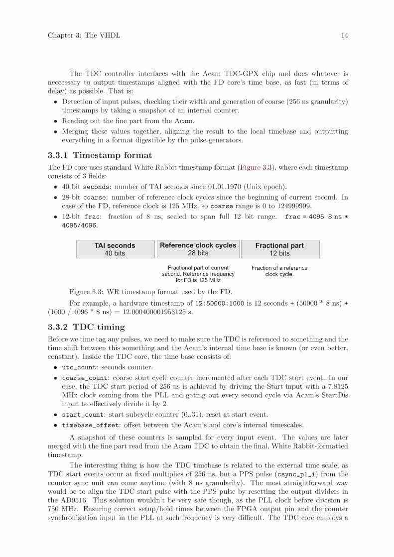
The FD core uses standard White Rabbit timestamp format (Figure 3.3), where each timestampconsists of 3 fields:
• 40 bit seconds: number of TAI seconds since 01.01.1970 (Unix epoch).
• 28-bit coarse: number of reference clock cycles since the beginning of current second. Incase of the FD, reference clock is 125 MHz, so coarse range is 0 to 124999999.
• 12-bit frac: fraction of 8 ns, scaled to span full 12 bit range. frac = 4095 8 ns *
4095/4096.
Figure 3.3: WR timestamp format used by the FD.
For example, a hardware timestamp of 12:50000:1000 is 12 seconds + (50000 * 8 ns) +
(1000 / 4096 * 8 ns) = 12.000400001953125 s.
3.3.2 TDC timing
Before we time tag any pulses, we need to make sure the TDC is referenced to something and thetime shift between this something and the Acam’s internal time base is known (or even better,constant). Inside the TDC core, the time base consists of:
• utc_count: seconds counter.
• coarse_count: coarse start cycle counter incremented after each TDC start event. In ourcase, the TDC start period of 256 ns is achieved by driving the Start input with a 7.8125MHz clock coming from the PLL and gating out every second cycle via Acam’s StartDisinput to effectively divide it by 2.
• start_count: start subcycle counter (0..31), reset at start event.
• timebase_offset: offset between the Acam’s and core’s internal timescales.
A snapshot of these counters is sampled for every input event. The values are latermerged with the fine part read from the Acam TDC to obtain the final, White Rabbit-formattedtimestamp.
The interesting thing is how the TDC timebase is related to the external time scale, asTDC start events occur at fixed multiplies of 256 ns, but a PPS pulse (csync_p1_i) from thecounter sync unit can come anytime (with 8 ns granularity). The most straightforward waywould be to align the TDC start pulse with the PPS pulse by resetting the output dividers inthe AD9516. This solution wouldn’t be very safe though, as the PLL clock before division is750 MHz. Ensuring correct setup/hold times between the FPGA output pin and the countersynchronization input in the PLL at such frequency is very difficult. The TDC core employs a

Chapter 3: The VHDL 15
simple trick here: when a resync pulse comes, it stores the difference between the lowest bits ofthe csync_coarse counter and the start subcycle counter (timebase_offset signal in p_start_
subcycle_counter process). This difference is added to the timestamps at the postprocessingstage to compensate for time base shift. See Figure 3.4 for a graphical explanation.
Figure 3.4: TDC core time base signals.
3.3.3 Input stage and TDC control
This part of the core takes care of the coarse input pulse and TDC start/stop enable signals. Itis responsible for:
• Sampling coarse pulse input. This is done in the p_sync_trigger process which implementsa simple rising edge detector with a 2-stage synchronizer and input enable/disable logic.
• Safely enabling and disabling the TDC input. There are three processes involved here: p_
safety_counter, which disables the input after a rising edge of and re-enables it a certaintime (c_FALLING_REENABLE_TIMEOUT) after the falling edge of the currently processed pulse.This prevents the core from generating incorrect timestamps when the input pulses come tooclose to each other or in case of poor quality or noise on the falling edge of the signal, whichcould be misinterpreted as a spurious input event. Even if the signal quality is fine, suchspurious pulses may occur while plugging the trigger input to a live signal. The remainingprocesses: p_gen_acam_start_dis and p_gen_acam_stop drive the TDC’s START andSTOP disable signals. The former ensures that the start input is not enabled in the middleof a rising edge of the 7.125 MHz start clock and gates the StartDis TDC input to effectivelydivide the start clock by 2. The latter enables the stop input when the TDC has receivedat least one correct start pulse.
• Rejecting pulses that do not meet the requirements. In our case - shorter than 24 nsor containing glitches. Width detection is done in the main state machine (p_main_fsm)by shifting in subsequent samples into a register (width_check_sreg) and checking if theregister contains only ones. Glitch detection exploits sensitivity of Acam’s Stop input:since we disable the trigger input right after we have detected a rising edge, the Acam shallnormally produce only one timestamp. Therefore, if the FIFO does not become emptyimmediately after read, a spurious pulse must have been tagged. Such situation may occurwhen the board is fed with a train of densely spaced pulses (where the shift register doesn’tnotice the gaps between them, but the Acam does). If any glitch or incorrect pulse isdetected, the timestamp is ignored, and the Acam is reset by asserting AluTrigger line.
• Reading out the Acam FIFO, done by the main state machine. After detecting a rising edgeon the coarse pulse input, the FSM waits for the timestamp to appear in Acam’s FIFO andreads it out from register 8. Several wait states are introduced by the FSM to ensure theread sequence does not cause setup/hold violations or signal integrity (SI) problems. Thefine value is passed along with the coarse counters and offsets to the postprocessing unit.

Chapter 3: The VHDL 16
3.3.4 Timestamp postprocessing
The postprocessor combines the fine value read from the Acam with the coarse value capturedusing a counter into a WR-compatible timestamp and aligns it to selected time base. Postpro-cessing is done in the p_postprocess_tags process. It consists of 4 pipelined stages:
• Subtract the start offset value from the fine part. Acam’s ALU can’t handle nega-tive numbers, therefore each timestamp is internally adjusted by a value defined in theStartOff[1,2] Acam’s control registers. This step subtracts this value (programmable viaASOR register, so that a pulse that occured in phase with a start pulse gets a fine value nearto 0. Some timestamps may have negative fine values after start offsest subtraction. Thisresults from the internal Acam’s delays - sometimes it may reference a stop event to a startevent that occured afterwards. The range of fine values is therefore wider than the startperiod - an event occuring 250 ns after a start pulse can be either timestamped as 250 or-6 ns.
• Rescale the fine value from Acam (expressed as a number of 41 ps bins) to WR time format(where 1 ps = 8 ns / 4096). This is done by simply multiplying by a constant scalefactor(programmable via the ADSFR register).
• Check consistency between the coarse counter coarse_count and the fine part. In idealcase, the final timestamp should be a simple sum of coarse_count * 256 ns and the finepart. In The Real World, transitions of the fine value (i.e. 256 ns to 0 ns) in the Acam arenot consistent with transitions of the coarse counter in the FPGA. Acam’s internal start isshifted forward with respect to the FPGA’s start signal. In certain cases, the fine part mayhave already flipped the 256 ns boundary, while the coarse counter has not counted up yet,producing a timestamp with an error of 256 ns (see Figure 3.5). Also, big fine values at thethe end of the range may be interleaved with negative ones, depending on Acam’s mood.
The postprocessor mitigates this problem by using the start_count counter. If start_
count value is low (indicating that we are close to the beginning of an FPGA start cycle),while the fine part is high (meaning that the TDC has not yet noticed the “fresh” startpulse), the timestamp’s coarse_count need to be adjusted by subtracting one start period.Thresholds for the comparisons are programmable via ATMCR register, their values wereobtained experimentally.
• Align the timestamp to our local/WR timebase, by simply adding the timebase_offset
value obtained during time base counter resynchronization.
Figure 3.5: Relations between coarse and fine timestamp parts.
As a result, we get a WR-formatted timestamp, which may have a constant offset withrespect to the WR/local timescale. This offset results from PCB trace lengths, componentproperties and the choice of the postprocessing register values and is compensated in softwareby adding a correction to all timestamps read from the card and all programmed delay values.The correction value is determined individually for each mezzanine during factory or DDMTDcalibration and written in the calibration EEPROM. Typical value is 127.5 ns.
Note that the postprocessor can be disabled for debugging purposes by setting TSBCR.RAW
bit. In such case, raw counter and fine values are written to the buffer instead of the finaltimestamp. This feature is used in production tests.
Chapter 3: The VHDL 17
3.3.5 Statistics unit
The Acam core includes a statistics unit. Its purpose is to collect data that may be helpful indebugging and performance tuning of the core:
• Count all detected input pulses.
• Count pulses that have been correctly tagged.
• Measure worst-case input-to-timestamp latency (which is important for delay applicationsas it defines minimum safe delay value). In case of the Acam configured in G-Mode, thelatency is 360 ns.
3.3.6 Acam host interface
The main TDC state machine lets the host directly access Acam’s control registers. Host (a.k.a.bypass) mode is active when GCR.BYPASS bit is set. The Acam must be programmed for G-modeoperation prior to enabling the hardware readout. In order to write a single Acam register followthe procedure below:
• Set the address of the Acam register by programming the GPIO expander.
• Write the desired word to TDR register.
• Write 1 to TDCSR.WRITE bit.
• Wait at least 1 microsecond before commencing another write.
Read procedure is quite similar:
• Set the address of the Acam register by programming the GPIO expander.
• Write 1 to TDCSR.READ bit.
• Wait at least 1 microsecond.
• Read the value returned by Acam from TDR register.
Note that once the TDC is programmed, its address (via the SPI expander) must beset to 8 (Acam FIFO1 register), so that the FSM can read correct data from the right FIFOregister.
3.3.7 Host timestamp readout
Relevant files: fd_ts_buffer.vhd.
The FD provides the values of all input and output timestamps through a 1024-entry ringbuffer. Each timestamp is associated with a sequence number and the source channel identifier.Timestamp readout can be enabled anytime and for any mode of operation (delay/TDC/pulsegenerator). The readout procedure goes as follows:
• Set channels we are interested in reading from in TSBCR.CHAN_MASK. Enable readout bysetting TSBCR.ENABLE.
• Poll the buffer by reading TSBCR.EMPTY bit or by handling the TS buffer interrupt. Do notattempt both ways simultaneously.
• Read the timestamp from TSBR registers. Order doesn’t matter.
• Release the timestamp from the buffer and proceed to the next one by writing anything tothe TSBR_ADVANCE register.
In case of an overflow, the oldest timestamps in the buffer are subsequently replaced bythe most recent ones. Loss of timestamps due to overflow can be detected by comparing thesequence numbers. If the buffer is handled through interrupts, coalescing mechanism is providedto reduce CPU load for larger amounts of timestamps. See TSBIR register description for details.
Chapter 3: The VHDL 18
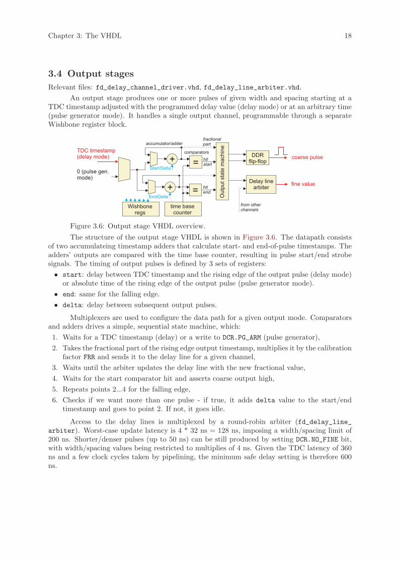
3.4 Output stages
Relevant files: fd_delay_channel_driver.vhd, fd_delay_line_arbiter.vhd.
An output stage produces one or more pulses of given width and spacing starting at aTDC timestamp adjusted with the programmed delay value (delay mode) or at an arbitrary time(pulse generator mode). It handles a single output channel, programmable through a separateWishbone register block.
Figure 3.6: Output stage VHDL overview.
The structure of the output stage VHDL is shown in Figure 3.6. The datapath consistsof two accumulateing timestamp adders that calculate start- and end-of-pulse timestamps. Theadders’ outputs are compared with the time base counter, resulting in pulse start/end strobesignals. The timing of output pulses is defined by 3 sets of registers:
• start: delay between TDC timestamp and the rising edge of the output pulse (delay mode)or absolute time of the rising edge of the output pulse (pulse generator mode).
• end: same for the falling edge.
• delta: delay between subsequent output pulses.
Multiplexers are used to configure the data path for a given output mode. Comparatorsand adders drives a simple, sequential state machine, which:
1. Waits for a TDC timestamp (delay) or a write to DCR.PG_ARM (pulse generator),
2. Takes the fractional part of the rising edge output timestamp, multiplies it by the calibrationfactor FRR and sends it to the delay line for a given channel,
3. Waits until the arbiter updates the delay line with the new fractional value,
4. Waits for the start comparator hit and asserts coarse output high,
5. Repeats points 2...4 for the falling edge,
6. Checks if we want more than one pulse - if true, it adds delta value to the start/endtimestamp and goes to point 2. If not, it goes idle.
Access to the delay lines is multiplexed by a round-robin arbiter (fd_delay_line_arbiter). Worst-case update latency is 4 * 32 ns = 128 ns, imposing a width/spacing limit of200 ns. Shorter/denser pulses (up to 50 ns) can be still produced by setting DCR.NO_FINE bit,with width/spacing values being restricted to multiplies of 4 ns. Given the TDC latency of 360ns and a few clock cycles taken by pipelining, the minimum safe delay setting is therefore 600ns.
Chapter 3: The VHDL 19
3.4.1 Programming the output stage
• Set the mode in DCR.MODE bit.
• Set the absolute start time or delay and pulse spacing in DCR.x_START, DCR.x_END andDCR.x_DELTA registers.
• Acknowledge the changes by writing DCR.UPDATE bit.
• If the output is not already enabled, write DCR.ENABLE bit and enable the correspondingSSR switch through the SPI GPIO.
3.4.2 Other important things
• The design is highly pipelined to meet timing for a 125 MHz clock with a rather widedatapath (40 + 28 + 12 = 80 bit add/compare operations).
• Start/end/delta and mode selection registers are shadowed to ensure atomic updates ofoutput pulse timings. By shadowing we mean that there are each of these registers has aninternal copy that is used by the output logic. All copies are updated simultaneously whenDCR.UPDATE bit is written.
• Offset resulting from pipelining and data path delays is systematic and must be compensatedby adjusting the start/end values in the software.
• Checking if the output has triggered can be done by polling DCR.PG_TRIG bit.
• FRR register must be initialized with correct calibration coefficient (see Section 4.2 [Outputstage calibration], page 24).
3.5 Other logic
3.5.1 OneWire
The FD core incorporates a dedicated Dallas’s 1-Wire bus master core for accessing the tem-perature sensor/ID chip from a non-deterministic host (1-Wire requires tight timing to operatecorrectly). The core’s documentation is available at the Opencores project page [6].
3.5.2 I2C
There is also a simple bit-banged I2C master for talking with the I2C EEPROM, accessiblethrough the I2CR register. The driver uses it for retreiving calibration data and identificationof the mezzanine.
3.5.3 SPI Master
The SPI Master is a specialized core (not a general-purpose Wishbone SPI master), accessiblevia the SCR register and interfacing with all SPI peripherals (VCXO DAC, GPIO and AD9516).Special features include:
• Two concurrent, arbitrated write ports: software via SCR register and hardware via tm_
dac_value port.
• The hardware port takes priority over software access and lets the SoftPLL update theVCXO DAC in a deterministic way, regardless of driver’s accesses to the GPIO and PLLchips.
• Atomic read/write access thanks to a single control/status/data register.
Chapter 3: The VHDL 20
3.5.4 Testing logic
There are two extra cores used during production testing and characterization of the card:
• A PWM driver, accessible via the TDER2 register. Used in lab tests for driving a Peltiermodule in order to characterize the temperature effects on the mezzanine.
• A frequency meter (TDER1), measuring the mezzanine’s VCXO frequency against the car-rier’s system clock. Used to characterize the tuning range of the oscillator during productiontest.
3.6 Initializing the card
Since initialization of the FD mezzanine is not simple and straightforward, a brief descriptionof the procedure is provided below:
1. Check for presence of the FD core by verifying IDR register.
2. Check mezzanine presence through GCR.FMC_PRESENT bit.
3. Read the calibration EEPROM via the I2C master. Parse and verify its contents.
4. Reset the mezzanine via RSTR register. Hold the FD core (except SPI & I2C) in reset.
5. Program the AD9516 PLL. Use register values included with the driver/test program code.
6. Initialize 1-wire temperature sensor. Read card serial number and temperature.
7. Initialize MCP23S17 GPIO. Disable termination, select internal trigger, disable all outputs.
8. Clocks are initialized, un-reset the core through RSTR register.
9. Enable TDC host mode by setting GCR.BYPASS bit.
10. Program the TDC in I-Mode. Run output stage calibration. Store calibrated values.
11. Program the TDC in G-Mode. Disable bypass and trigger input.
12. Load timestamp postprocessor configuration (ADSFR, ASOR, ATMCR values). Use values pro-vided in the test program.
13. Set board time to 0 via TCR register.
14. Purge timestamp readout buffer (TSBCR.PURGE bit).
15. Enable trigger input via GCR register.
Now the card should be ready for timestamp readout and output programming. For codeexamples please look at fdelay_lib.c file in the test program [3].

Chapter 3: The VHDL 21
3.7 Carrier implementation example
Relevant files: svec_top.vhd.
An example FD VHDL core implementation on a SVEC FMC carrier [8] is shown inFigure 3.7.
Figure 3.7: Implementation of two FD cores on a SVEC carrier.
The top level is only a passive interconnect between the FD cores, White Rabbit andFPGA-specific blocks, such as clock/IO buffers and PLLs. The components of our exampledesign are:
• 2 FD cores,
• White Rabbit core, providing synchronization and Ethernet connectivity,
• Additional White Rabbit components: GTP serdes wrapper and SPI DAC driver,
• Wishbone interconnect,
• Etherbone core, allowing for Ethernet access to entire memory space of the card,
• Vectored Interrupt Controller (VIC), multiplexing interrupts from all sources (in our case,the two FD cores). VIC’s vector table is preinitialized with base addresses of the coressourcing interrupts to enable automatic IRQ line detection,
• VME64x core, bridging between VME64x bus and Wishbone (with all necessary VMEbuffers/tristates),
• Clock distribution and PLLs (producing the DDMTD and system clocks and DDR clocksfor the output stages of the FD cores),
• Utility cores - power up reset and SVEC front panel LED driver for status indication.
For more details, refer to the source files and comments inside.

Chapter 4: Calibration procedures 22
4 Calibration procedures
4.1 Output stage calibration
The role of this calibration mechanism is to make sure the SY89295 fine delay lines introducedelays consistent with the programmed settings. In The Ideal World, the tap size of a SY89295is 10 ps, so programming the chip to 800 shall result with a delay of 8 ns. In reality, the tapsize depends on PVT effects - we observed that some chips, when set to 800 taps produce 7.5ns or 8.5 ns instead of the requested 8 ns. As mentioned earlier, the FD output stage worksby producing an 8 ns resolution coarse pulse with a counter and adjusting it precisely in anSY99295 chip, according to the equation:
t_measured = floor(t_out / 8ns) + FRR * (t_out mod 8ns)
where t_measured is the measured timestamp of the output pulse, and t_out is the onethe output stage was requested to produce. The FRR parameter relates the fractional (modulo)part of the timestamp with the number of fine delay line taps required to accurately reproduceit. In The Ideal World, it should be 100 taps/ns. If the alpha value is wrong, output pulses willbe imprecise. To make things worse, the error will not be proportional to the requested delay,but only to its modulo part. Therefore, pulses whose timestamps have small fractional value(for example, 1000 ns mod 8 ns = 0) will have no error at all, while other ones (e.g. 1007.9 ns)will have an error of as much as 1 ns.
Since there is absolutely no corellation between the pulses coming to the TDC and thecard’s reference clock, fractional parts of the input timestamps and the values written to theSY89295 for each output pulse look purely random. Therefore, one pulse may have an error of0, while the next one might be off by almost a nanosecond - an effect that in technical terms iscalled huge, non-gaussian jitter, exceeding by far the 100 ps specification requirement.
Figure 4.1: Effects of uncalibrated output delay line.
Fortunately, this effect is mitigated by calibrating the FRR value for each SY89295 delayline. This is done every time the card starts up.
The output stage calibration mechanism is depicted in Figure 4.2. It works by feedingthe output stage with calibration pulses and measuring the in-out delay of SY89295 delays fordifferent tap settings in order to find a point at which they delay the signal by exactly 8 nsmore than at tap setting of 0. The TDC, reconfigured in the I-mode (single ended start inputand 4 single ended stop inputs, one per output) is reused as a calibrator (thanks to its’ voltageadjusting PLL, we know that its definition of 8 ns is not worse than of the reference oscillator).Precision better than 10 ps rms (single tap) is achieved by averaging multiple measurements.This calibration is performed by the device driver every time the card is initialized. In order tospeed up calibration, the software assumes monotonicity of the delay line (guaranteed by design)and instead of sweeping all possible tap counts, employs a simple divide-and-conquer algorithm.

Chapter 4: Calibration procedures 23
Figure 4.2: Output stage jitter calibration mechanism.
Note that while the calibration in progress, the output switch is disabled to stop ourcalibration pulses from reaching devices driven by the card. This unfortunately prevents exe-cuting the calibration during runtime without risk of losing pulses. We provided an alternativemechanism to overcome this limitation, which exploits the fact that since process and supplyvoltage remain constant during operation, only temperature has significant impact on the out-put stage delay. A function of 8 ns tap delay error vs temperature was measured in the lab bycooling/heating up the card to temperatures between 30 and 90 degrees C with a Peltier celland is used to relate the temperature and 8ns tap setting measured at the card startup with its’current temperature. Simple 2nd order polynomial fitting allows for updating the output stagescale factor without disturbing the outputs with extra calibration pulses.
The same method (with full range sweeping instead of divide-and-conquer) is used tomeasure linearity (INL/DNL) of the delay lines during production test.
Chapter 4: Calibration procedures 24
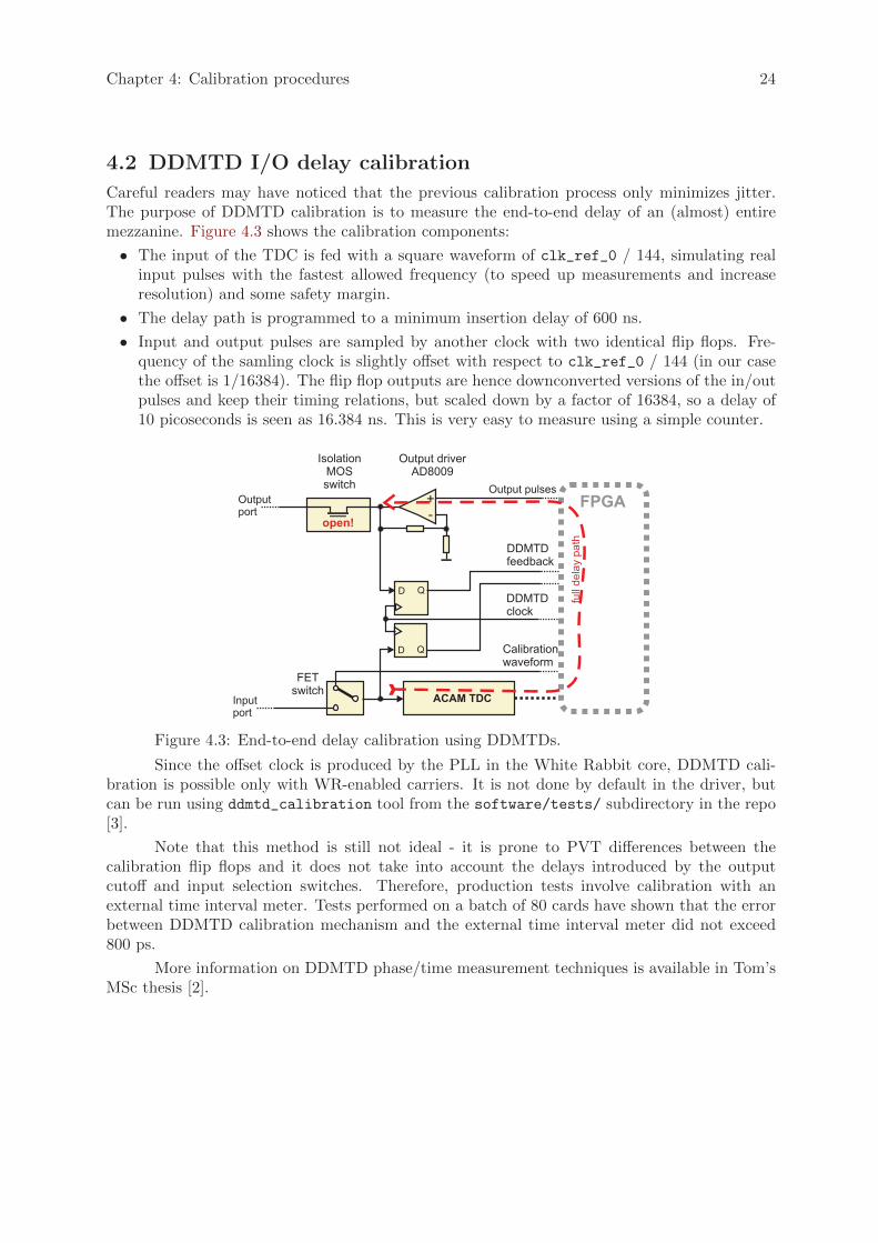
4.2 DDMTD I/O delay calibration
Careful readers may have noticed that the previous calibration process only minimizes jitter.The purpose of DDMTD calibration is to measure the end-to-end delay of an (almost) entiremezzanine. Figure 4.3 shows the calibration components:
• The input of the TDC is fed with a square waveform of clk_ref_0 / 144, simulating realinput pulses with the fastest allowed frequency (to speed up measurements and increaseresolution) and some safety margin.
• The delay path is programmed to a minimum insertion delay of 600 ns.
• Input and output pulses are sampled by another clock with two identical flip flops. Fre-quency of the samling clock is slightly offset with respect to clk_ref_0 / 144 (in our casethe offset is 1/16384). The flip flop outputs are hence downconverted versions of the in/outpulses and keep their timing relations, but scaled down by a factor of 16384, so a delay of10 picoseconds is seen as 16.384 ns. This is very easy to measure using a simple counter.
Figure 4.3: End-to-end delay calibration using DDMTDs.
Since the offset clock is produced by the PLL in the White Rabbit core, DDMTD cali-bration is possible only with WR-enabled carriers. It is not done by default in the driver, butcan be run using ddmtd_calibration tool from the software/tests/ subdirectory in the repo[3].
Note that this method is still not ideal - it is prone to PVT differences between thecalibration flip flops and it does not take into account the delays introduced by the outputcutoff and input selection switches. Therefore, production tests involve calibration with anexternal time interval meter. Tests performed on a batch of 80 cards have shown that the errorbetween DDMTD calibration mechanism and the external time interval meter did not exceed800 ps.
More information on DDMTD phase/time measurement techniques is available in Tom’sMSc thesis [2].

Chapter 5: Registers description 25
5 Registers description
5.1 Memory layout
Base Address Core0x000 Main registers. See Section 5.2.1 [Main registers], page 250x100 Channel 1 registers. See Section 5.3.1 [Output stage registers], page 370x200 Channel 2 registers. See Section 5.3.1 [Output stage registers], page 370x300 Channel 3 registers. See Section 5.3.1 [Output stage registers], page 370x400 Channel 4 registers. See Section 5.3.1 [Output stage registers], page 370x500 1-wire master registers
5.2 Main registers
The main register block controls all subsystems of the FD core excluding the OneWire ther-mometer and output channels.
5.2.1 Memory map summary
Address Type Prefix Name0x0 REG RSTR Reset Register0x4 REG IDR ID Register0x8 REG GCR Global Control Register0xc REG TCR Timing Control Register0x10 REG TM_SECH Time Register - TAI seconds (MSB)0x14 REG TM_SECL Time Register - TAI seconds (LSB)0x18 REG TM_CYCLES Time Register - sub-second 125 MHz clock cycles0x1c REG TDR Host-driven TDC Data Register.0x20 REG TDCSR Host-driven TDC Control/Status0x24 REG CALR Calibration register0x28 REG DMTR_IN DMTD Input Tag Register0x2c REG DMTR_OUT DMTD Output Tag Register0x30 REG ADSFR Acam Scaling Factor Register0x34 REG ATMCR Acam Timestamp Merging Control Register0x38 REG ASOR Acam Start Offset Register0x3c REG IECRAW Raw Input Events Counter Register0x40 REG IECTAG Tagged Input Events Counter Register0x44 REG IEPD Input Event Processing Delay Register0x48 REG SCR SPI Control Register0x4c REG RCRR Reference Clock Rate Register0x50 REG TSBCR Timestamp Buffer Control Register0x54 REG TSBIR Timestamp Buffer Interrupt Register0x58 REG TSBR_SECH Timestamp Buffer Readout Seconds Register (MSB)0x5c REG TSBR_SECL Timestamp Buffer Readout Seconds Register (LSB)0x60 REG TSBR_
CYCLES
Timestamp Buffer Readout Cycles Register
0x64 REG TSBR_FID Timestamp Buffer Readout Fine/Channel/Sequence IDRegister
0x68 REG I2CR I2C Bit-banged IO Register0x6c REG TDER1 Test/Debug Register 10x70 REG TDER2 Test/Debug Register 1
Chapter 5: Registers description 26
0x74 REG TSBR_
DEBUG
Timestamp Buffer Debug Values Register
0x78 REG TSBR_
ADVANCE
Timestamp Buffer Advance Register
0x80 REG EIC_IDR Interrupt disable register0x84 REG EIC_IER Interrupt enable register0x88 REG EIC_IMR Interrupt mask register0x8c REG EIC_ISR Interrupt status register
5.2.2 RSTR - Reset Register
Controls software reset of the Fine Delay core and the mezzanine connected to it. Both resetlines are driven indepentently, there is also an unlock word provided to prevent resetting theboard/core by accidentally accessing this register.
Bits Access Prefix Default Name0 W/O RST_FMC 0 State of the reset Line of the Mezzanine
(EXT RST N pin)
1 W/O RST_CORE 0 State of the reset of the Fine Delay Core31...16 W/O LOCK 0 Reset magic value
Field DescriptionRST_FMC write 0: FMC is held in reset
write 1: Normal FMC operation
RST_CORE write 0: FD Core is held in resetwrite 1: Normal FD Core operation
LOCK Protection field - the state of FMC and core lines willonly be updated if LOCK is written with 0xdead together with the new state ofthe reset lines.
5.2.3 IDR - ID Register
Magic identification value (for detecting FD cores by the driver). Even though now enumerationis handled through SDB, the IDR register is kept for compatibility with older software.
Bits Access Prefix Default Name31...0 R/O IDR 0xf19ede1a ID Magic Value
Field DescriptionIDR Equal to 0xf19ede1a
5.2.4 GCR - Global Control Register
Common control bits used throughout the core.
Bits Access Prefix Default Name0 R/W BYPASS 0 Bypass hardware TDC controller1 R/W INPUT_EN 0 Enable trigger input2 R/O DDR_
LOCKED
X PLL lock status
3 R/O FMC_
PRESENT
X Mezzanine present

Chapter 5: Registers description 27
Field DescriptionBYPASS Descides who is in charge of the TDC and delay lines:
write 0: TDC and delay lines are controlled by the HDL core (normal operationmode)write 1: TDC and delay lines controlled from the host via TDR and TDCSR
registers (calibration and testing mode)
INPUT_EN write 1: trigger input is enabledwrite 0: trigger input is disabledNote 1: state of INPUT_EN is relevant only in normal operation mode (i.e. whenGCR.BYPASS == 0).Note 2: enabling the input in INPUT_EN does not mean it will be automaticallyenabled in the ACAM TDC - one must pre-program its registers first.
DDR_LOCKED read 1: AD9516 and internal DDR PLLs are lockedread 0: AD9516 or internal DDR PLL not (yet) locked
FMC_PRESENT Mirrors the state of the FMC’s PRSNT_L hardware pin:read 1: FMC card is present (PRSNT_L == 0)read 0: no FMC card in the slot (PRSNT_L == 1)
5.2.5 TCR - Timing Control Register
Controls time setting and White Rabbit/local time base selection.
Bits Access Prefix Default Name0 R/O DMTD_STAT X DMTD Clock Status1 R/W WR_ENABLE 0 WR Timing Enable2 R/O WR_LOCKED X WR Timing Locked3 R/O WR_
PRESENT
X WR Core Present
4 R/O WR_READY X WR Core Time Ready5 R/O WR_LINK X WR Core Link Up6 W/O CAP_TIME 0 Capture Current Time7 W/O SET_TIME 0 Set Current Time
Field DescriptionDMTD_STAT Status of the DMTD (helper) clock, used for DDMTD calibration purposes by
the test suite.read 0: DMTD clock is not available or has been lost since last read operationof TCR registerread 1: DMTD clock has been OK since previous read of TCR register
WR_ENABLE Enables/disables WR synchronization.write 1: WR synchronization is enabled. Poll the TCR.WR_LOCKED bit to checkif the WR Core is still locked.write 0: WR synchronization is disabled, the card is in free running mode.Note: enabling WR synchronization will cause a jump in the time base counterof the core. This may lead to lost pulses, therefore it is strongly recommendeddo disable the inputs/outputs before entering WR mode. When WR mode isdisabled, the core will continue counting without a jump.
WR_LOCKED Status of WR synchronization.read 0: local oscillator/time base is not locked to WR (or a transient delockevent occured since last read of TCR register).read 1: local oscillator is syntonized to WR and local timebase is aligned withWR time.

Chapter 5: Registers description 28
WR_PRESENT Indicates whether we have a WR Core associated with this Fine Delay Core.Reflects the state of the g_with_wr_core generic HDL parameter.read 0: No WR Core present. Enabling WR will have no effect.read 1: WR Core available.
WR_READY Indicates the status of synchronization of the associated WR core. Valid onlyif TCR.WR_PRESENT bit is set.read 0: WR Core is not synchronzied yet: there is no link, no PTP master inthe network or synchronization is in progress.read 1: WR Core time is ready. User may enable WR reference by settingTCR.WR_ENABLE bit.Note: it is allowed to enable the WR mode even if TCR.WR_READY or TCR.WR_
LINK bits are not set. Time base will be synced to WR as soon as the core getscorrect PTP time from the master.
WR_LINK Reflects the state of the WR Core’s Ethernet link. Provided as an additionaldiagnostic feature.read 0: Ethernet link is down.read 1: Ethernet link is up.
CAP_TIME Performs an atomic read of the core’s current time.write 1: transfers the current value of seconds/cycles counters to TM_ registers.write 0: no effect.
SET_TIME Sets internal time base counter to a given time in an atomic way:write 1: transfers the current value of TM_ registers to the timebase counter.write 0: no effect.Note 1: Internal time counters must be always initialized to a known value (e.g.zeroes), after every reset/power cycle.Note 2: Writing to TCR.SET_TIME while WR mode is active is forbidden. Ifyou do so, prepare for unforeseen consequences.
5.2.6 TM_SECH - Time Register - TAI seconds (MSB)
Seconds counter, most significant partread: value of internal seconds counter taken upon last write to TCR.CAP_TIME bit.write: new value of seconds counter (loaded to the time base counter by writing TCR.SET_TIME
bit)
Bits Access Prefix Default Name7...0 R/W TM_SECH X TAI seconds (MSB)
5.2.7 TM_SECL - Time Register - TAI seconds (LSB)
Seconds counter, least significant partread: value of internal seconds counter taken upon last write to TCR.CAP_TIME bit.write: new value of seconds counter (loaded to the time base counter by writing TCR.SET_TIME
bit)
Bits Access Prefix Default Name31...0 R/W TM_SECL X TAI seconds (LSB)
5.2.8 TM_CYCLES - Time Register - sub-second 125 MHz clock cycles
Number of 125 MHz reference clock cycles from the beginning of the current second.read: value of cycles counter taken upon last write to TCR.CAP_TIME bit.write: new value of cycles counter (loaded to the time base counter by writing TCR.SET_TIME
bit)
Chapter 5: Registers description 29
Bits Access Prefix Default Name27...0 R/W TM_CYCLES X Reference clock cycles (0...124999999)
5.2.9 TDR - Host-driven TDC Data Register.
Holds the 28-bit data word read from/to be written to the ACAM TDC, when the core isconfigured in bypass mode (GCR.BYPASS == 1).
Bits Access Prefix Default Name27...0 R/W TDR X TDC Data
5.2.10 TDCSR - Host-driven TDC Control/Status
Allows controlling the TDC directly from the host (when GCR.BYPASS == 1).
Bits Access Prefix Default Name0 W/O WRITE 0 Write to TDC1 W/O READ 0 Read from TDC2 R/O EMPTY X Empty flag3 W/O STOP_EN 0 Stop enable4 W/O START_DIS 0 Start disable5 W/O START_EN 0 Start enable6 W/O STOP_DIS 0 Stop disable7 W/O ALUTRIG 0 Pulse <code>Alutrigger</code> line
Field DescriptionWRITE Writes the data word from TDR register to the ACAM TDC.
write 1: write the data word programmed in TDR register to the TDC. TheTDC address must be set via the SPI I/O expander.write 0: no effect.
READ Reads a data word from the TDC and puts it in TDR register.write 1: read a data word from the TDC. The read word will be put in TDR
register. The TDC address must be set via the SPI I/O expander.write 0: no effect.
EMPTY Raw status of the EF (FIFO empty) pin of the TDC.read 0: there is one (or more) pending timestamp(s) in the ACAM’s internalFIFO.read 1: the internal TDC FIFO is empty (no timestamps to read).
STOP_EN Controls the StopDis input of the TDC.write 1: enables the TDC stop input.write 0: no effect.
START_DIS Controls the StartDis input of the TDC.write 1: disables the TDC start input.write 0: no effect.
START_EN Controls the StartDis input of the TDC.write 1: enables the TDC start input.write 0: no effect.
STOP_DIS Controls the StopDis input of the TDC.write 1: disables the TDC stop input.write 0: no effect.
Chapter 5: Registers description 30
ALUTRIG Controls the TDC’s Alutrigger line. Depending on the TDC’s configuration,it can be used as a reset/FIFO clear/trigger signal.write 1: generates a pulse ACAM’s Alutrigger linewrite 0: no effect.
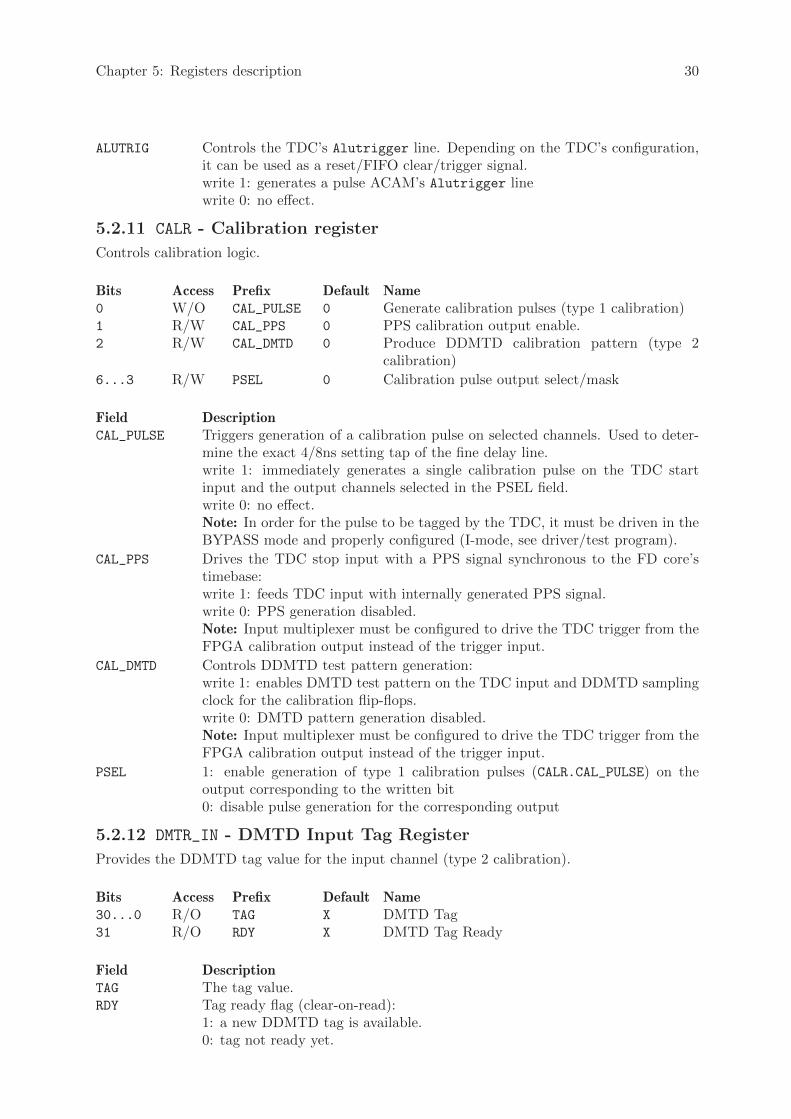
5.2.11 CALR - Calibration register
Controls calibration logic.
Bits Access Prefix Default Name0 W/O CAL_PULSE 0 Generate calibration pulses (type 1 calibration)1 R/W CAL_PPS 0 PPS calibration output enable.2 R/W CAL_DMTD 0 Produce DDMTD calibration pattern (type 2
calibration)
6...3 R/W PSEL 0 Calibration pulse output select/mask
Field DescriptionCAL_PULSE Triggers generation of a calibration pulse on selected channels. Used to deter-
mine the exact 4/8ns setting tap of the fine delay line.write 1: immediately generates a single calibration pulse on the TDC startinput and the output channels selected in the PSEL field.write 0: no effect.Note: In order for the pulse to be tagged by the TDC, it must be driven in theBYPASS mode and properly configured (I-mode, see driver/test program).
CAL_PPS Drives the TDC stop input with a PPS signal synchronous to the FD core’stimebase:write 1: feeds TDC input with internally generated PPS signal.write 0: PPS generation disabled.Note: Input multiplexer must be configured to drive the TDC trigger from theFPGA calibration output instead of the trigger input.
CAL_DMTD Controls DDMTD test pattern generation:write 1: enables DMTD test pattern on the TDC input and DDMTD samplingclock for the calibration flip-flops.write 0: DMTD pattern generation disabled.Note: Input multiplexer must be configured to drive the TDC trigger from theFPGA calibration output instead of the trigger input.
PSEL 1: enable generation of type 1 calibration pulses (CALR.CAL_PULSE) on theoutput corresponding to the written bit0: disable pulse generation for the corresponding output
5.2.12 DMTR_IN - DMTD Input Tag Register
Provides the DDMTD tag value for the input channel (type 2 calibration).
Bits Access Prefix Default Name30...0 R/O TAG X DMTD Tag31 R/O RDY X DMTD Tag Ready
Field DescriptionTAG The tag value.RDY Tag ready flag (clear-on-read):
1: a new DDMTD tag is available.0: tag not ready yet.

Chapter 5: Registers description 31
5.2.13 DMTR_OUT - DMTD Output Tag Register
Provides the DDMTD tag value for a selected output channel (type 2 calibration).
Bits Access Prefix Default Name30...0 R/O TAG X DMTD Tag31 R/O RDY X DMTD Tag Ready
Field DescriptionTAG The tag value.RDY Tag ready flag (clear-on-read):
1: a new DDMTD tag is available.0: tag not ready yet.
5.2.14 ADSFR - Acam Scaling Factor Register
Scaling factor between the FD’s internal time scale and the ACAM’s format. Used only innormal operating mode (GCR.BYPASS == 0).Formula (for G-Mode): ADSFR = round(2097.152 * ACAM_bin_size [ps])
Bits Access Prefix Default Name17...0 R/W ADSFR 0 ADSFR Value
5.2.15 ATMCR - Acam Timestamp Merging Control Register
Controls merging of fine timestamps prouced by Acam with coarse timestamps obtained by theFPGA.
Bits Access Prefix Default Name7...0 R/W C_THR 0 Coarse threshold30...8 R/W F_THR 0 Fine threshold
5.2.16 ASOR - Acam Start Offset Register
ACAM timestamp start offset. Value that gets subtracted from ACAM’s timestamps (due toACAM’s ALU architecture that does not support negative numbers).
Bits Access Prefix Default Name22...0 R/W OFFSET 0 Start Offset
5.2.17 IECRAW - Raw Input Events Counter Register
TDC debugging & statistics register
Bits Access Prefix Default Name31...0 R/O IECRAW X Number of raw events.
Field DescriptionIECRAW Number of all input pulses detected by the timestamper.
5.2.18 IECTAG - Tagged Input Events Counter Register
TDC debugging & statistics register
Bits Access Prefix Default Name

Chapter 5: Registers description 32
31...0 R/O IECTAG X Number of tagged events
Field DescriptionIECTAG Number of all input pulses which passed width/glitch checks and were correctly
timestamped.
5.2.19 IEPD - Input Event Processing Delay Register
TDC debugging & statistics register
Bits Access Prefix Default Name0 W/O RST_STAT 0 Reset stats8...1 R/O PDELAY X Processing delay
Field DescriptionRST_STAT Write 1: resets the delay/pulse count counters (IECRAW, IECTAG and
IEPD.PDELAY)write 0: no effect
PDELAY Worst-case delay between an input event and its timestamp being available.Expressed as a number of 125 MHz clock cycles.
5.2.20 SCR - SPI Control Register
Single control register for the SPI Controller, allowing for atomic updates of the DAC, GPIOand PLL.
Bits Access Prefix Default Name23...0 R/W DATA X Data24 R/W SEL_DAC 0 Select DAC25 R/W SEL_PLL 0 Select PLL26 R/W SEL_GPIO 0 Select GPIO27 R/O READY X Ready flag28 R/W CPOL 0 Clock Polarity29 W/O START 0 Transfer Start
Field DescriptionDATA Data to be read/written from/to the SPI busSEL_DAC write 1: selects the DAC as the target peripheral of the transfer
write 0: no effect
SEL_PLL write 1: selects the AD9516 PLL as the target peripheral of the transferwrite 0: no effect
SEL_GPIO write 1: selects the MCP23S17 GPIO as the target peripheral of the transferwrite 0: no effect
READY read 0: SPI controller is busy performing a transferread 1: SPI controller has finished its previous transfer. Read-back data isavailable in SCR.DATA
CPOL 0: SPI clock is not inverted (data valid on rising edge)1: SPI clock is inverted (data valid on falling edge)
START write 1: starts SPI transfer from/to the selected peripheralwrite 0: no effect
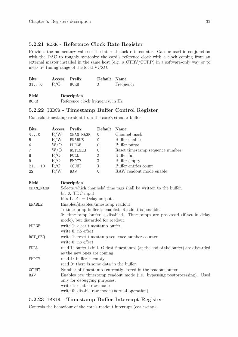
Chapter 5: Registers description 33
5.2.21 RCRR - Reference Clock Rate Register
Provides the momentary value of the internal clock rate counter. Can be used in conjunctionwith the DAC to roughly syntonize the card’s reference clock with a clock coming from anexternal master installed in the same host (e.g. a CTRV/CTRP) in a software-only way or tomeasure tuning range of the local VCXO.
Bits Access Prefix Default Name31...0 R/O RCRR X Frequency
Field DescriptionRCRR Reference clock frequency, in Hz
5.2.22 TSBCR - Timestamp Buffer Control Register
Controls timestamp readout from the core’s circular buffer
Bits Access Prefix Default Name4...0 R/W CHAN_MASK 0 Channel mask5 R/W ENABLE 0 Buffer enable6 W/O PURGE 0 Buffer purge7 W/O RST_SEQ 0 Reset timestamp sequence number8 R/O FULL X Buffer full9 R/O EMPTY X Buffer empty21...10 R/O COUNT X Buffer entries count22 R/W RAW 0 RAW readout mode enable
Field DescriptionCHAN_MASK Selects which channels’ time tags shall be written to the buffer.
bit 0: TDC inputbits 1..4: = Delay outputs
ENABLE Enables/disables timestamp readout:1: timestamp buffer is enabled. Readout is possible.0: timestamp buffer is disabled. Timestamps are processed (if set in delaymode), but discarded for readout.
PURGE write 1: clear timestamp buffer.write 0: no effect
RST_SEQ write 1: reset timestamp sequence number counterwrite 0: no effect
FULL read 1: buffer is full. Oldest timestamps (at the end of the buffer) are discardedas the new ones are coming.
EMPTY read 1: buffer is empty.read 0: there is some data in the buffer.
COUNT Number of timestamps currently stored in the readout bufferRAW Enables raw timestamp readout mode (i.e. bypassing postprocessing). Used
only for debugging purposes.write 1: enable raw modewrite 0: disable raw mode (normal operation)
5.2.23 TSBIR - Timestamp Buffer Interrupt Register
Controls the behaviour of the core’s readout interrupt (coalescing).

Chapter 5: Registers description 34
Bits Access Prefix Default Name9...0 R/W TIMEOUT 0 IRQ timeout [milliseconds]21...10 R/W THRESHOLD 0 Interrupt threshold
Field DescriptionTIMEOUT The IRQ line will be asserted after TSBIR.TIMEOUT milliseconds even if the
amount of data in the buffer is below TSBIR.THRESHOLD.
THRESHOLD Minimum number of samples (timestamps) in the buffer that immediately trig-gers an interrupt.
5.2.24 TSBR_SECH - Timestamp Buffer Readout Seconds Register(MSB)
Bits Access Prefix Default Name7...0 R/O TSBR_SECH X Timestamps TAI Seconds (bits 39-32)
5.2.25 TSBR_SECL - Timestamp Buffer Readout Seconds Register(LSB)
Bits Access Prefix Default Name31...0 R/O TSBR_SECL X Timestamps TAI Seconds (bits 31-0)
5.2.26 TSBR_CYCLES - Timestamp Buffer Readout Cycles Register
Bits Access Prefix Default Name27...0 R/O TSBR_
CYCLES
X Timestamps cycles count (in 8 ns ticks)
5.2.27 TSBR_FID - Timestamp Buffer Readout Fine/Channel/SequenceID Register
Bits Access Prefix Default Name3...0 R/O CHANNEL X Channel ID15...4 R/O FINE X Fine Value (in phase units)31...16 R/O SEQID X Timestamp Sequence ID
Field DescriptionCHANNEL ID of the originating channel:
0: TDC input1..4: outputs 1..4
5.2.28 I2CR - I2C Bit-banged IO Register
Controls state of the mezzanine’s I2C bus lines by means of bitbanging
Bits Access Prefix Default Name0 R/W SCL_OUT 1 SCL Line out1 R/W SDA_OUT 1 SDA Line out2 R/O SCL_IN X SCL Line in3 R/O SDA_IN X SDA Line in

Chapter 5: Registers description 35
Field DescriptionSCL_OUT write 0: drive SCL to 0
write 1: drive SCL to weak 1 (pullup)
SDA_OUT write 0: drive SDA to 0write 1: drive SDA to weak 1 (pullup)
SCL_IN State of the SCL line.SDA_IN State of the SDA line.
5.2.29 TDER1 - Test/Debug Register 1
Bits Access Prefix Default Name31...0 R/O VCXO_FREQ X VCXO Frequency
Field DescriptionVCXO_FREQ Mezzanine VCXO frequency in Hz, measured using the system clock as a ref-
erence. Used during factory test only.
5.2.30 TDER2 - Test/Debug Register 1
Bits Access Prefix Default Name31...0 R/W PELT_
DRIVE
0 Peltier PWM drive
Field DescriptionPELT_DRIVE Peltier module PWM drive. Lab-only feature for measuring temperature char-
acteristics of the board.
5.2.31 TSBR_DEBUG - Timestamp Buffer Debug Values Register
Bits Access Prefix Default Name31...0 R/O TSBR_
DEBUG
X Debug value
Field DescriptionTSBR_DEBUG Additional register for holding timestamp debug data (used only in raw readout
mode). Content format is not specified.
5.2.32 TSBR_ADVANCE - Timestamp Buffer Advance Register
Bits Access Prefix Default Name0 W/O ADV 0 Advance buffer readout
5.2.33 EIC_IDR - Interrupt disable register
Writing 1 disables handling of the interrupt associated with corresponding bit. Writin 0 has noeffect.
Bits Access Prefix Default Name0 W/O TS_BUF_
NOTEMPTY
0 Timestamp Buffer interrupt.
1 W/O DMTD_SPLL 0 DMTD SoftPLL interrupt

Chapter 5: Registers description 36
2 W/O SYNC_
STATUS
0 Sync Status Changed
Field Descriptionts_buf_
notempty
write 1: disable interrupt ’Timestamp Buffer interrupt.’write 0: no effect
dmtd_spll write 1: disable interrupt ’DMTD SoftPLL interrupt’write 0: no effect
sync_status write 1: disable interrupt ’Sync Status Changed’write 0: no effect
5.2.34 EIC_IER - Interrupt enable register
Writing 1 enables handling of the interrupt associated with corresponding bit. Writin 0 has noeffect.
Bits Access Prefix Default Name0 W/O TS_BUF_
NOTEMPTY
0 Timestamp Buffer interrupt.
1 W/O DMTD_SPLL 0 DMTD SoftPLL interrupt2 W/O SYNC_
STATUS
0 Sync Status Changed
Field Descriptionts_buf_
notempty
write 1: enable interrupt ’Timestamp Buffer interrupt.’write 0: no effect
dmtd_spll write 1: enable interrupt ’DMTD SoftPLL interrupt’write 0: no effect
sync_status write 1: enable interrupt ’Sync Status Changed’write 0: no effect
5.2.35 EIC_IMR - Interrupt mask register
Shows which interrupts are enabled. 1 means that the interrupt associated with the bitfield isenabled
Bits Access Prefix Default Name0 R/O TS_BUF_
NOTEMPTY
X Timestamp Buffer interrupt.
1 R/O DMTD_SPLL X DMTD SoftPLL interrupt2 R/O SYNC_
STATUS
X Sync Status Changed
Field Descriptionts_buf_
notempty
read 1: interrupt ’Timestamp Buffer interrupt.’ is enabledread 0: interrupt ’Timestamp Buffer interrupt.’ is disabled
dmtd_spll read 1: interrupt ’DMTD SoftPLL interrupt’ is enabledread 0: interrupt ’DMTD SoftPLL interrupt’ is disabled
sync_status read 1: interrupt ’Sync Status Changed’ is enabledread 0: interrupt ’Sync Status Changed’ is disabled
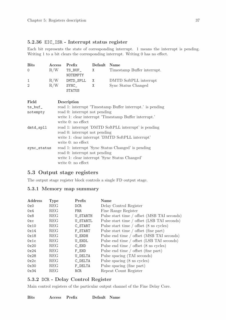
Chapter 5: Registers description 37
5.2.36 EIC_ISR - Interrupt status register
Each bit represents the state of corresponding interrupt. 1 means the interrupt is pending.Writing 1 to a bit clears the corresponding interrupt. Writing 0 has no effect.
Bits Access Prefix Default Name0 R/W TS_BUF_
NOTEMPTY
X Timestamp Buffer interrupt.
1 R/W DMTD_SPLL X DMTD SoftPLL interrupt2 R/W SYNC_
STATUS
X Sync Status Changed
Field Descriptionts_buf_
notempty
read 1: interrupt ’Timestamp Buffer interrupt.’ is pendingread 0: interrupt not pendingwrite 1: clear interrupt ’Timestamp Buffer interrupt.’write 0: no effect
dmtd_spll read 1: interrupt ’DMTD SoftPLL interrupt’ is pendingread 0: interrupt not pendingwrite 1: clear interrupt ’DMTD SoftPLL interrupt’write 0: no effect
sync_status read 1: interrupt ’Sync Status Changed’ is pendingread 0: interrupt not pendingwrite 1: clear interrupt ’Sync Status Changed’write 0: no effect
5.3 Output stage registers
The output stage register block controls a single FD output stage.
5.3.1 Memory map summary
Address Type Prefix Name0x0 REG DCR Delay Control Register0x4 REG FRR Fine Range Register0x8 REG U_STARTH Pulse start time / offset (MSB TAI seconds)0xc REG U_STARTL Pulse start time / offset (LSB TAI seconds)0x10 REG C_START Pulse start time / offset (8 ns cycles)0x14 REG F_START Pulse start time / offset (fine part)0x18 REG U_ENDH Pulse end time / offset (MSB TAI seconds)0x1c REG U_ENDL Pulse end time / offset (LSB TAI seconds)0x20 REG C_END Pulse end time / offset (8 ns cycles)0x24 REG F_END Pulse end time / offset (fine part)0x28 REG U_DELTA Pulse spacing (TAI seconds)0x2c REG C_DELTA Pulse spacing (8 ns cycles)0x30 REG F_DELTA Pulse spacing (fine part)0x34 REG RCR Repeat Count Register
5.3.2 DCR - Delay Control Register
Main control registers of the particular output channel of the Fine Delay Core.
Bits Access Prefix Default Name

Chapter 5: Registers description 38
0 R/W ENABLE 0 Enable channel1 R/W MODE 0 Delay mode select2 W/O PG_ARM 0 Pulse generator arm3 R/O PG_TRIG X Pulse generator triggered4 W/O UPDATE 0 Update delay/absolute trigger time5 R/O UPD_DONE X Delay update done flag6 W/O FORCE_DLY 0 Force calibration delay7 R/W NO_FINE 0 Disable fine part update8 R/W FORCE_HI 0 Force output high
Field DescriptionENABLE write 0: channel is disabled. Output is driven LOW.
write 1: channel is enabled. Output may produce pulses.
MODE 0: Channel will work as a delay generator, producing delayed copies of pulsescoming to the trigger input. Start/End registers shall contain delays of respec-tively, the rising and falling edge.1: Channel will work as a programmable pulse generator - producing a pulsewhich begins and ends at absolute TAI times stored in Start/End registers.Note: MODE bit can be safely set only when the delay logic is disabled (i.e. whenDCR.ENABLE == 0)
PG_ARM write 1: arms the pulse generator.write 0: no effect.Note: The values written to [U/C/F]_START and [U/C/F]_END must be biggerby at least 300 ns than the value of the UTC counter at the moment of armingthe pulse generator. In practice, the safety margin should be much higher, asit’s affected by the non-determinism of the operating system.
PG_TRIG read 1: pulse generator has been triggered and produced a pulseread 0: pulse generator is busy or hasn’t triggered yet
UPDATE write 1: Starts the update procedure. The start and end times from[U/C/F][START/END] will be transferred in an atomic way to the internal de-lay/pulse generator registers.write 0: no effect.Note: Care must be taken when updating the delay value - if the channel getsstuck due to invalid control values written, the only way to bring it back aliveis to disable and re-enable it by toggling DCR.ENABLE bit.
UPD_DONE read 1: the delays from [U/C/F][START/END] have been loaded into internalregisters. Subsequent triggers will be delayed by the newly programmed value.read 0: update operation in progress
FORCE_DLY Used in type 1 calibration.write 1: preloads the SY89295 delay line with the contents of FRR register.write 0: no effect
NO_FINE write 1: disables updating of the fine part of the pulse delay to allow for pro-ducing faster signals (i.e. pulse width/spacing < 200 ns), at the cost of lessaccurate width/spacing control (multiple of 4 ns).write 0: normal operation. Pulse width/spacing must be at least 200 ns,width/spacing resolution is 10 ps.Note: A typical use case for NO_FINE bit is producing a 10 MHz clock.
FORCE_HI write 1: forces constant 1 on the output when the channel is disabledwrite 0: forces constant 0 on the output when the channel is disabledUsed for testing/calibration purposes.
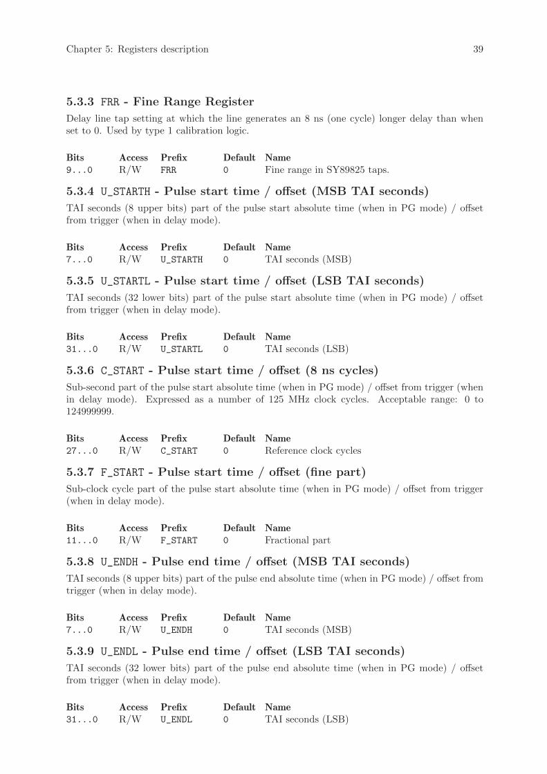
Chapter 5: Registers description 39
5.3.3 FRR - Fine Range Register
Delay line tap setting at which the line generates an 8 ns (one cycle) longer delay than whenset to 0. Used by type 1 calibration logic.
Bits Access Prefix Default Name9...0 R/W FRR 0 Fine range in SY89825 taps.
5.3.4 U_STARTH - Pulse start time / offset (MSB TAI seconds)
TAI seconds (8 upper bits) part of the pulse start absolute time (when in PG mode) / offsetfrom trigger (when in delay mode).
Bits Access Prefix Default Name7...0 R/W U_STARTH 0 TAI seconds (MSB)
5.3.5 U_STARTL - Pulse start time / offset (LSB TAI seconds)
TAI seconds (32 lower bits) part of the pulse start absolute time (when in PG mode) / offsetfrom trigger (when in delay mode).
Bits Access Prefix Default Name31...0 R/W U_STARTL 0 TAI seconds (LSB)
5.3.6 C_START - Pulse start time / offset (8 ns cycles)
Sub-second part of the pulse start absolute time (when in PG mode) / offset from trigger (whenin delay mode). Expressed as a number of 125 MHz clock cycles. Acceptable range: 0 to124999999.
Bits Access Prefix Default Name27...0 R/W C_START 0 Reference clock cycles
5.3.7 F_START - Pulse start time / offset (fine part)
Sub-clock cycle part of the pulse start absolute time (when in PG mode) / offset from trigger(when in delay mode).
Bits Access Prefix Default Name11...0 R/W F_START 0 Fractional part
5.3.8 U_ENDH - Pulse end time / offset (MSB TAI seconds)
TAI seconds (8 upper bits) part of the pulse end absolute time (when in PG mode) / offset fromtrigger (when in delay mode).
Bits Access Prefix Default Name7...0 R/W U_ENDH 0 TAI seconds (MSB)
5.3.9 U_ENDL - Pulse end time / offset (LSB TAI seconds)
TAI seconds (32 lower bits) part of the pulse end absolute time (when in PG mode) / offsetfrom trigger (when in delay mode).
Bits Access Prefix Default Name31...0 R/W U_ENDL 0 TAI seconds (LSB)
Chapter 5: Registers description 40
5.3.10 C_END - Pulse end time / offset (8 ns cycles)
Sub-second part of the pulse end absolute time (when in PG mode) / offset from trigger (whenin delay mode). Expressed as a number of 125 MHz clock cycles. Acceptable range: 0 to124999999.
Bits Access Prefix Default Name27...0 R/W C_END 0 Reference clock cycles
5.3.11 F_END - Pulse end time / offset (fine part)
Sub-clock cycle part of the pulse end absolute time (when in PG mode) / offset from trigger(when in delay mode).
Bits Access Prefix Default Name11...0 R/W F_END 0 Fractional part
5.3.12 U_DELTA - Pulse spacing (TAI seconds)
TAI seconds between the rising edges of subsequent output pulses.
Bits Access Prefix Default Name3...0 R/W U_DELTA 0 TAI seconds
5.3.13 C_DELTA - Pulse spacing (8 ns cycles)
Reference clock cycles between the rising edges of subsequent output pulses.
Bits Access Prefix Default Name27...0 R/W C_DELTA 0 Reference clock cycles
5.3.14 F_DELTA - Pulse spacing (fine part)
Sub-cycle part of spacing between the rising edges of subsequent output pulses.
Bits Access Prefix Default Name11...0 R/W F_DELTA 0 Fractional part
5.3.15 RCR - Repeat Count Register
Register controlling the number of output pulses to be generated upon reception of a triggerpulse or triggering the channel in PG mode.
Bits Access Prefix Default Name15...0 R/W REP_CNT 0 Repeat Count16 R/W CONT 0 Continuous Waveform Mode
Field DescriptionREP_CNT Equal to desired number of pulses minus 1 (0 = 1 pulse, 0xffff = 65536 pulses)CONT write 1: output will produce a contiguous square wave upon reception of trigger
pulse. The generation can be aborted only disabling the channel (clearingDCR.ENABLE)write 0: each trigger will produce RCR.REP_CNT+1 pulses.
Chapter 6: References 41
6 References
1. Official schematics and PCB design (CERN EDMS)
https://edms.cern.ch/nav/EDA-02267-V5-2
2. Tom’s MSc thesis (a bible of White Rabbit timing)
http://www.ohwr.org/documents/80
3. Hardware homepage & Wiki
http://www.ohwr.org/projects/fmc-delay-1ns-8cha
4. Official user’s manual
http://www.ohwr.org/documents/179
5. Acam TDC-GPX datasheet
http://www.acam.de/fileadmin/Download/pdf/English/DB_GPX_e.pdf
6. Sockit 1-Wire master project page
http://opencores.org/
7. Git repository with VHDL & test program sources
http://ohwr.org/projects/fmc-delay-1ns-8cha/repository
8. SVEC FMC Carrier project
http://ohwr.org/projects/svec
9. Software Described Bus (SDB) project
http://www.ohwr.org/projects/fpga-config-space
10. Fine Delay Production Test System
http://www.ohwr.org/projects/pts
11. Analog Devices PLL design software (AdiSimClk)
http://www.analog.com/en/rf-tools/adisimclk/topic.html
12. wbgen2 - a Wishbone slave generator
http://www.ohwr.org/projects/wishbone-gen