finding the power/area limits of cmos…ultra.usc.edu/assets/002/39691.pdf · mike chen stanley...
TRANSCRIPT

Berkeley Wireless Research Center
Finding the power/area limits of CMOS…
Bob BrodersenBob BrodersenIan O’DonnellIan O’Donnell
Mike ChenMike ChenStanley Wang Stanley Wang
Short Range UWB Radio Systems
Berkeley Wireless Research Center
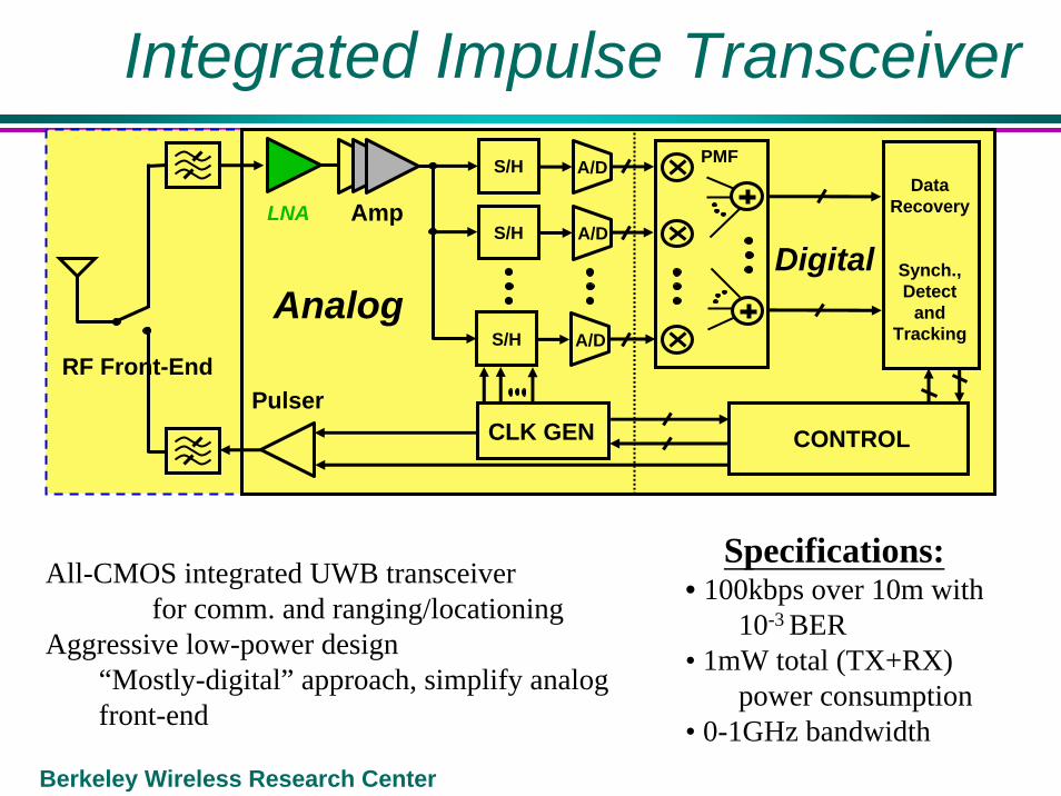
Integrated Impulse Transceiver
RF Front-End
LNA
Pulser
A/DS/H
A/DS/H
A/DS/H
PMFData
Recovery
Synch.,Detect
andTracking
CLK GEN CONTROL
AnalogDigital
Amp
Specifications:• 100kbps over 10m with
10-3 BER • 1mW total (TX+RX)
power consumption• 0-1GHz bandwidth
All-CMOS integrated UWB transceiverfor comm. and ranging/locationing
Aggressive low-power design“Mostly-digital” approach, simplify analog front-end

Berkeley Wireless Research Center
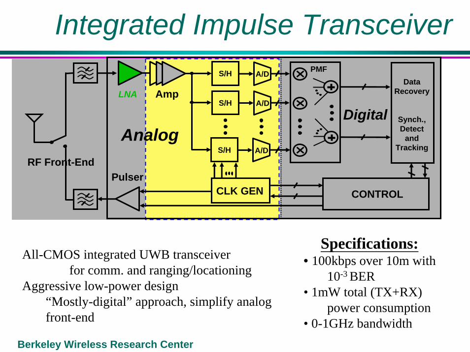
Integrated Impulse Transceiver
RF Front-End
LNA
Pulser
A/DS/H
A/DS/H
A/DS/H
PMFData
Recovery
Synch.,Detect
andTracking
CLK GEN CONTROL
AnalogDigital
Amp
Specifications:• 100kbps over 10m with
10-3 BER • 1mW total (TX+RX)
power consumption• 0-1GHz bandwidth
All-CMOS integrated UWB transceiverfor comm. and ranging/locationing
Aggressive low-power design“Mostly-digital” approach, simplify analog front-end

Berkeley Wireless Research Center
3-10 GHz UWB CMOS LNA (Stanley Wang)
Common-gate input stage with input matchingInter-stage matching network also provides current gain due to the impedance mismatchAll inductors are pattern ground shielded, except Lload. Increases SRF and decreases Q (increasing BW)..13 micron technology14 mW, 1 mm2

Berkeley Wireless Research Center
Layout sensitivity
1mm0.
83m
m
2-stage input matching“Aggressive” layout strategy
1.54mm
1.13
mm
3-stage input matching“Conservative” layout strategy
Keep distance between L’sSingle-turn inductors

Berkeley Wireless Research Center
Measurement Results
0 5 10 15-20
-15
-10
-5
0
5
10
15
Frequency (GHz)
Mag
nitu
de (d
B)
3-stage 2-stage
0 5 10 15-70
-60
-50
-40
-30
-20
-10
0
Frequency (GHz)
Mag
nitu
de (d
B)
S22
S12
2 4 6 8 10 123
4
5
6
7
8
9
10
11
Frequency (GHz)
NF
(dB)
2-stage
3-stage
0 5 10 15-50
-40
-30
-20
-10
0
Frequency (GHz)
Mag
nitu
de (d
B)
3-stage
2-stage
Berkeley Wireless Research Center
Integrated Impulse Transceiver
RF Front-End
LNA
Pulser
A/DS/H
A/DS/H
A/DS/H
PMFData
Recovery
Synch.,Detect
andTracking
CLK GEN CONTROL
AnalogDigital
Amp
Specifications:• 100kbps over 10m with
10-3 BER • 1mW total (TX+RX)
power consumption• 0-1GHz bandwidth
All-CMOS integrated UWB transceiverfor comm. and ranging/locationing
Aggressive low-power design“Mostly-digital” approach, simplify analog front-end

Berkeley Wireless Research Center
UWB Transceiver Prototype
Based on Digital Sampling/Acquisition Oscilloscopes
TIA
PULSE
GAIN ADC
DLL
Control Logicand
Interface
ADC
ADC
CLKGEN
BIAS OSC
Analog Front-End
DigitalInterface
Pulser (byStanley Wang)

Berkeley Wireless Research Center
The Integrated implementation…2.8 x 4.7 mm2 (13.2 mm2)
Bias
Test Output BufferTIA
Variable Gain Stages
ADC DLL
ControlTransmitter
CLK
Oscillator
Digital Interface Logic

Berkeley Wireless Research Center
Pulse Transmission & Reception
Berkeley Wireless Research Center
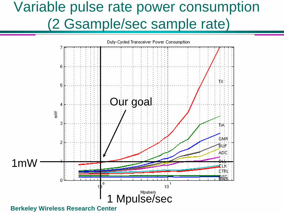
Variable pulse rate power consumption(2 Gsample/sec sample rate)
1mW
1 Mpulse/sec
Our goal

Berkeley Wireless Research Center
Integrated Impulse Transceiver
RF Front-End
LNA
Pulser
A/DS/H
A/DS/H
A/DS/H
PMFData
Recovery
Synch.,Detect
andTracking
CLK GEN CONTROL
AnalogDigital
Amp
Specifications:• 100kbps over 10m with
10-3 BER • 1mW total (TX+RX)
power consumption• 0-1GHz bandwidth
All-CMOS integrated UWB transceiverfor comm. and ranging/locationing
Aggressive low-power design“Mostly-digital” approach, simplify analog front-end
Berkeley Wireless Research Center
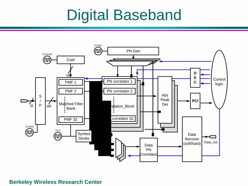
Digital Baseband
Coef
160
128
PN correlator 1
PN correlator 2
PN correlator 32
CLK
PN GenCLKcoef
CLKpn
AbsPeakDet
DataRecover
(soft/hard)
Controllogic
Correlation_Block
Data_out
SymbolStrobe
DataPN
Correlator
PCI
DEC
CLKwin
S/P32
PMF 1
PMF 2
PMF 32
Matched FilterBank

Berkeley Wireless Research Center
UWB Baseband Chip
Process: 0.13um (ST Microelectronics)Size: 3.6mm x 3.3mm Standard Cells: 530,000
MOPS/mW: 1,500Power:Acquisition 12 mW Tracking 1.5 mW
@ 1.08 V, 10 MHz clk

Berkeley Wireless Research Center
3-10 GHz Transceiver Analytic and Sub-sampling for Impulse Processing (Mike Chen)
Sample at below NyquistAnalytic signaling reduces the sensitivity to timing offsetsProvides fine timing resolution
Mostly digital solution
A/D is critical component
∑

Berkeley Wireless Research Center
Asynchronous ADC prototype
• Asynchronous SAR ADC architecture to meet speed requirement
• 600 Msamples/Sec, 6 bits 5 mW, .12 mm2!!
• Input 3dB bandwidth > 4GHz Sub-sampling RF8 Gigasamples/sec < 100mW
Highlights:

Berkeley Wireless Research Center
Time-interleaved 2X Async. ADC
No clock higher than the sampling frequency

Berkeley Wireless Research Center
A/D Performance

Berkeley Wireless Research Center
Demonstrated .13 Micron CMOS capabilities
10 GHz LNA - at 10 mW and 1mm2
Impulse transceiver at 1 Megapulse/mWDSP baseband at 1.5 GigaOps/mWA/D at 600 Msamples/sec, 6 bit @ 5mW, .12mm2
Even more important is that these numbers will improve with scaling of the technology….