final report on nasa cooperative agreement ncc3-286
TRANSCRIPT

NASA-C_-201905
/
FINAL REPORT ON NASA COOPERATIVE
AGREEMENT NCC3-286
Alkali Layered Compounds Interfaces for Energy Conversion and
Energy storage
Start Date :
End Date :
01 / 20 / 95
01 / 29 / 96 _
The total approved budget for all three years was $ 503.645
( CAU Budget No : 243604 )
Dr. Chris A. Papageorgopoulos
Surface Physics Laboratory
Department of Physics
Clark Atlanta University
223 James P. Brawley Drive
Atlanta, Georgia 30214
Submitted To
National Aeronautics and Space AdministrationLewis Research Center
Contracts Support BranchAttn: Grants Officer
Mail Stop 500-315
Cleveland, Ohio 44135
NASA approved an extension from 01/20 95 to 06/30/96
YEAR ONE
TOTAL (YEAR ONE) $167,266
During Year One, I brought a complete new ultra-high vacuum (UHV) system equipped
with a specimen manipulator, an At+ ion sputterer, a low energy electron diffraction
(LEED) system, an Auger electron spectrometer (AES), a work function (WF)
measurement device with a Kelvin probe and related accessories. The total cost of these
items is approximately $170,000. The UHV system with the specimen manipulator, At+
ion sputterer and related accessories was obtained through other sources, totaling
approximately $100,000. In addition to the above surface analysis techniques of LEED,
AES, WF, and some accessories such as thermocouples, Ta, Ni and W wires, Ta foils of
different thicknesses, pure gases, etc., were also purchased through the present grant
(within the equipment budget).
On July, 1993, I visited the Photovoltaic Laboratory at NASA Lewis Research Center,
where I gave a talk on "Alkali Adsorption on Layered Compounds". After extensive
discussions with the staff, it was agreed that the thrust of our research efforts should be
redirected to support pressing problems within the Photovoltaic group. We agreed
specifically to study the Adsorption of chalcogenides on Si and 111-V compoundsemiconductors.
On September 1993 1 started receiving the ordered equipment; the UHV system and
surface analysis techniques; an Auger electron spectrometer (AES), a Kelvin probe for
work function (WF) measurements and a low energy electron diffraction (LEED) system.
By the end of the year 1993 all the purchased equipment were put together, and the UHV
system was brought to acceptable operating condition.
Much of the necessary equipment, however, was not available such as voltmeters, power
supplies, an oscilloscope, chart recorders, computers, liquid nitrogen and other pieces.
For a few days a week, we borrowed meters from the students' laboratory at Clark Atlanta
University. The Photovoltaic group at NASA Lewis Research Center gave us some
specimens of Si(100). In addition, Professor M. Kamaratos came from Greece on four-
month sabbatical, and the first Master's Degree graduate student, Aris Papageorgopoulos,
joined the group. And we thus began the _oposed investigation.
In the meanwhile, the continuation proposal for Year Two had been approved.

YEAR TWO
TOTAL (YEAR TWO) $181,511
During Year Two, we ordered a scanning tunneling microscope (STM) fro $116,000, a
quadrapole mass spectrometer, power supplies, a computer, a chart recorder, micro-
voltmeters, a thickness monitor, an evaporator with its power supply (for GaAs and InP
deposition), and related accessories. The total cost of these items was approximately
$175,000. Most of the items, other than the STM and some accessories, were obtained
through other sources totaling approximately $55,000.
Meanwhile, according to the collaboration agreement with the Photovoltaic group at
NASA, we started the systematic study on the adsorption of chalcogenides on Si and III-
V compound semiconductor surfaces. The study took place in the UHV with the available
techniques ofLEED, AES and WF measurements.
Specifically, we started with in in-situ adsorption study of elemental S on Ni(100). I
would like to note that this is the first time that elemental sulfur, as opposed to sulfur
compounds such as H2S, is deposited at RT. This innovation supports a preliminary
experiment with a prototype substrate such as Ni(100). The knowledge of the behavior of
S on Ni is of particular interest due to the poisoning effects of S on catalytic reactions
occurring on Ni surfaces. The results have been published in the Journal of Surface
Science (see reference 1).
Next, we continued with the study of: "Adsorption (passivation) of elemental S on
Si(100)2xl Surfaces". This study was also part of the thesis of Aris Papageorgopoulos.
Part of the results have been presented: at the 15th European Conference of Surface
Science, ECOSS-15, September, 1995, Lille, France, with the title "Adsorption of
elemental S on Si(100)2xl surfaces", Aris Papageorgopoulos, M. Kamaratos. The same
work with the same title has been accepted for publication by the Journal of Surface
Science (reference 2).
Additional results of S on Si(100)2xl surfaces were presented at the Mat. Res. Soc.
Meeting, December, 1995, Boston, Massachusetts, with the title "Passivation of
Si(100)2xl surfaces with elemental sulfur", Aris Papageorgopoulos. This paper has also
been accepted for publication in the Proceedings of Material Research Society Journal
(reference 3).
After completion of the study of S on Si(100)2x 1 surfaces, the results have been
submitted to Physical Review B (reference 4).
Meanwhile, at the end of the second year, we received the STM and the quadrapole mass
spectrometer, which we started to install.
In the mean time, the continuation proposal for Year Three has been approved.

YEAR THREE
TOTAL (YEAR THREE) $154,868
During this year we mounted the Scanning Tunneling Microscope (STM) on the existing
UHV system. Then we tried to get familiar with the specific type of STM and bring it to
acceptable operating conditions.
This year we bought a Hemispherical Analyzer for XPS-UPS measurements for $81,250,
which is mounted to a new UHV system, which is specially designed for XPS-UPS
measurements. The UHV system has been obtained through other sources.
Now going back to research, the investigation continues with the adsorption of Cs (alkali)
on S-covered Si(100)2xl surfaces. This was also the second part of Aris
Papageorgopoulos' thesis. The first results have been submitted for publication to Journal
of Surface Science (reference 5).
Subsequent results of Cs on S-covered Si(100) surfaces have been presented to the
International Conference on the Structure of Surfaces, July 8, 1996 (Aix-en Provence,
France). The title of this work was: "The behavior of Cs on S-covered Si(100)2xl and
Si(100)lxl surfaces". The same paper, with the same authors, has been submitted to
Surface Physics Review (reference 6).
The research activities continued with the adsorption of S on Cs-covered Si(100) surfaces.
This work has been completed, it will appear in the thesis of our second graduate student,
Adero Comer. The most important results of this work will be submitted for publication.
Presently, the third graduate student, Dwight Mosby, is working with the STM system and
specifically he tries to confirm the proposed structure models of S and Cs on Si(100)surfaces.
In the near future, we are going to continue with GaAs and InP substrates.

References
,
.
.
,
.
.
Adsorption of elemental S on Ni(100) surfaces
C. A. Papageorgopoulos, M. Kamaratos
Surface Science 338 (1995) 77-82.
Adsorption of elemental S on Si(100)2xl surfaces
Ads Papageorgopoulos, M. Kamaratos
Surfhce Sience 352-354 (1996) 364-368
Passivation of Si(100) 2x 1 surfaces with elemental sulfur
Aris Papageorgopoulos
Accepted for publication by Materials Research Society Symposium Proceedings1996.
Adsorption of elemental S on Si(100) 2xl: surface reconstruction
Axis Papageorgopoulos, Adero Corner, M. Kamaratos, C. A. Papageorgopoulos
Submitted for publication to Physical Review B.
Adsorption of Cs on S-covered Si(100) surfaces
Aris Papageorgopoulos, D. C. Papageorgopoulos
Submitted for publication to Surface Science.
The behavior of Cs on S-covered Si(100) 2xl and Si(100) Ixl surfaces
Aris Papageorgopoulos, Dwight Mosby Jr, C. A. Papageorgopoulos
Submitted for publication to Surface Physics Review.

fib, UIm,
ELSEVIER Surface Science 338 (1995) 77-82
surface science
i, Ames. IA,
urgh. PA
ttion at the end of this
;cription prices are avail-tme$ 82-92, and Surface
:_the following countries,. New Zealand. Pakistan.
1. 1000 AE Amsterdam.nonths of our publication
I and Earth Sciences; El
nail the tables of contents
:le will be supplied free of
hinted in The Netherlands
Adsorption of elemental S on Ni(100) surfaces
C.A. Papageorgopoulos "'1, M. Kamaratos 1
Department o[ Physics, Clark Atlanta University, James P. Brawley Drive at Fair Street S.W., Atlanta, GA 30314, USA
Received 9 September 1994; accepted for publication 21 March 1995
Abstract
We have studied the adsorption of elemental S on Ni(100) surfaces by LEED, AES, TDS and WF measurements in
UHV. We compared the measurements to those of reported investigations, most of which used HzS as sulfur source. The
elemental S, at room temperature, is grown on Ni(100) in a layer by layer mode. Sulfur forms the 1:)(2 x 2), initially, and
subsequently the 6(2 x 2) structure at the completion of the first S layer. The second layer is disordered. These findings are
in contrast with most of the published papers which report that the S on Ni(100) saturates in the first layer, its sticking
coefficient decreases drastically and it does not desorb before 1200 K. Deposition of S, at RT, increases the work function of
Ni by 0.25 eV. Heating before the desorption temperature (1100 K) of S causes: (a) a rearrangement of Ni atoms with a
possible diffusion of Ni from the bulk to the surface, having the tendency to interact with the S overlayer and (b) an increase
of the WF change close to 0.4 eV, the value reported after the exposure of Ni(100) to H2S and subsequent heating. The AES
and WF variation are related to a recently reported difference in electronic structure between the p(2 X 2)S and 6(2 X 2)S
structures.
Keywords: Auger electron spectroscopy; Low energy electron diffraction (LEED); Nickel; Silicon; Thermal desorption spectroscopy; Workfunction measurements
1. Introduction
The adsorption of sulfur on nickel surfaces has
been extensively studied in the past. The knowledge
of the behavior of S on Ni is of particular interest.
This is due to poisoning effects of S on catalytic
reactions occurring on Ni surfaces [1-3], and the
recent finding that sulfurization treatment is very
important in the passivation of different surfaces
[4-6]. The adsorption sites of S atoms, the changes
of the electronic properties of the surface, and the
substrate relaxation after S deposition on Ni surfaces
• Corresponding author.
1 Permanent address: Department of Physics, University of
loannina, P.O. Box 1186, GR-451 10 loannina, Greece.
have been studied by a variety of surface analysis
techniques [7-10].
Despite the amount of research, there are still
questions about the S-Ni system. Most of the S
adsorption studies, up to now, have taken place with
the exposure of the substrate surface to H2S gas. To
remove the H 2 from the surface the substrates were
heated to equal or greater than 200°C [10-15]. The
role of hydrogen and subsequent heating on the
growth mode of S alone on Ni(100), however, is not
known. For a detailed understanding of the adsorp-
tion kinetics of S on Ni surfaces at room tempera-
tures and lower, it is important to deposit elemental
sulfur.
In this work we evaporate elemental sulfur on
Ni(100) surfaces• We study the sample using low
003%6028/95/$09.50 © 1995 Elsevier Science B.V. All rights reservedSSD1 0039-6028(95)00489-0

78 C.A. Papageorgopoulos,M. Kamaratos / Surface Science 338 (1995) 77-82
..
, -',o !
energy electron diffraction (LEED), Auger electron
spectroscopy (AES), thermal desorption spec-troscopy (TDS), and work function (WF) measure-
ments. The measurements suggest kinetics of S and
Ni interaction during S deposition at room tempera-
ture (RT) and subsequent heating of Ni(100) sub-
strates which are reported for the first time.
2. Experimental
The experiments were performed in an ultra-high
vacuum chamber (p < 10 -l° Tort), equipped with a
cylindrical mirror analyzer (CMA) for AES and
EELS measurements, a quadrupole mass spectrome-
ter (QMS) for TDS measurements, a Kelvin probe
for WF measurements and a LEED system.
Elemental sulfur was evaporated by thermal dis-
sociation of MoS 2 single crystal flakes mounted on a
tungsten filament. During dissociation of MoS 2 the
Mo remained on the tungsten filament, while S was
evaporated. The Ni(100) substrate was cleaned byAr ÷ bombardment (1 kV, 5 /zA) for 20 min and
subsequent annealing at about 1000 K. This cycle
was repeated several times until the AES peak heightsof the main impurities (carbon and sulfur) were
almost negligible. The temperature of the sample
was measured by a Cr-AI thermocouple calibrated
with an infrared pyrometer in the range of 900-1200K.
3. Results and discussion
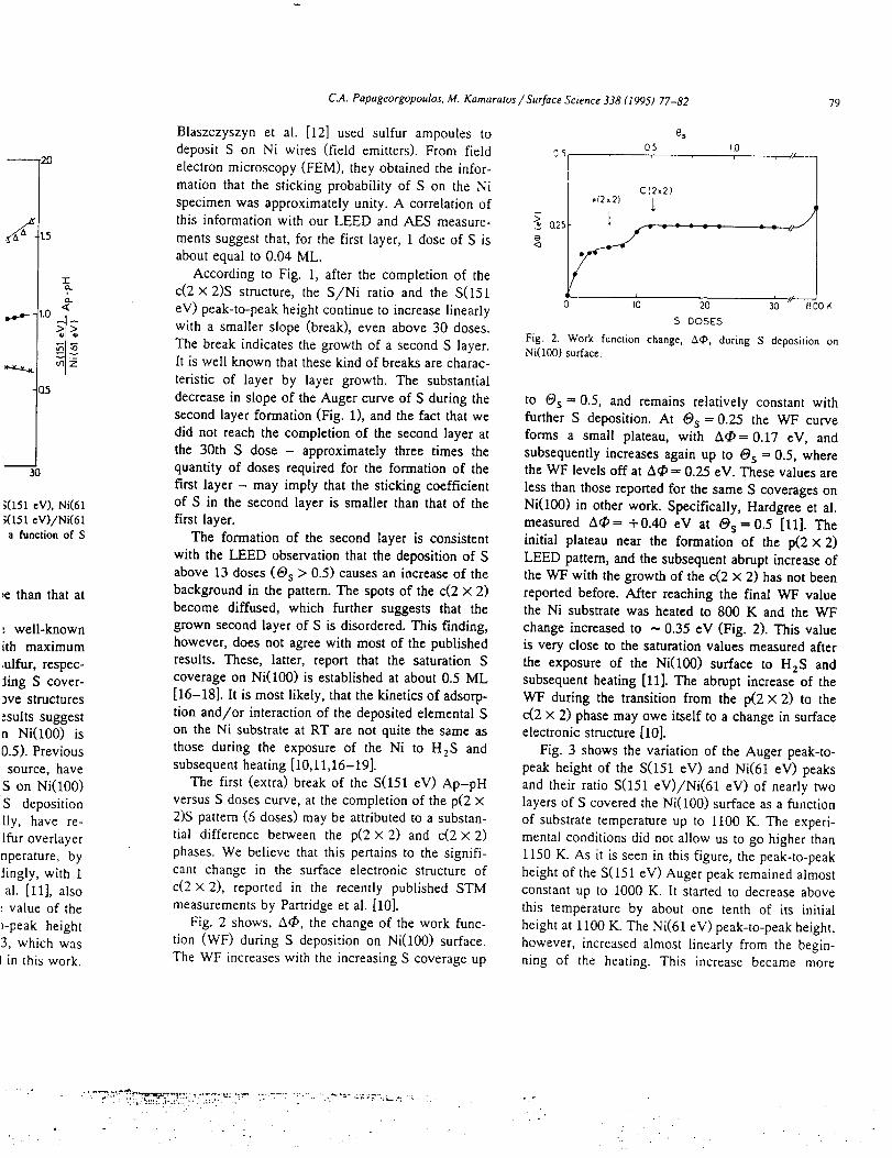
Fig. 1 shows the Auger peak-to-peak heights
(Ap-pH) of S(151 eV), Ni(61 eV) and their Auger
peak-to-peak height ratios, S(151 eV)/Ni(61 eV), in
correlation with the LEED patterns, as a function of
doses of S deposition. It is obvious, from this figure,
that the S/Ni ratio increases linearly with increasing
number of S doses, with a break (slope change of the
S/Ni ratio versus S doses curve) occurring at 13
doses. The peak-to-peak height of Ni(61 eV) de-
creases analogously with a break occurring at 13
doses of S. The peak-to-peak height of S(151 eV)
also increases linearly with increased doses of S. The
latter, however, forms two breaks. The expected at
13 doses, and an extra one at 6 doses of S deposi-
_S
O.5 1.02O
p(2 2) C(i2x2) _/a" 1.5
.J"2-C "r
20 1.o '_tX
%
1o -- ]IZ5
x Nit61 eV)
A SINi
0 1'0 20 305 DOSE5
Fig. 1. Auger peak-to-peakheight (Ap-pH) of $(151 eV), Ni(6!eV) and their Auger peak-to-peak height ratios,S(151 eV)/Ni(61eV), in correlation with the LEED patterns, as a function of Sdeposition doses.
tion, with a smaller change of the slope than that at13 doses.
The LEED observations show the well-known
patterns of p(2 × 2) and c(2 × 2) with maximum
spot intensities at 6 and 13 doses of sulfur, respec-
tively. We assume that the corresponding S cover-ages, _gs, at the completion of the above structures
are 0.25 and 0.5 monolayers. These results suggest
that the sticking coefficient of S on Ni(100) is
constant, at least up to 13 doses (8 s = 0.5). Previous
measurements, with H2S as the sulfur source, have
shown that the sticking coefficient of S on Ni(100)
surfaces decreases drastically with S deposition
[10,16-18]. Partridge et al. specifically, have re-
ported that the p(2 × 2) and c(2 × 2) sulfur overlayer
structures were obtained at room temperature, by
dosing the clean Ni surface, correspondingly, with 1
and 50 L of H2S [10]. Hardergree et al. [11], also
using an H2S source, reported that the value of the
S(152 eV)/Ni(61 eV) Auger peak-to-peak height
ratio at (9s = 0.5 was found to be 1.23, which was
very close to the ~ 1.26 value reported in this work.
Bias
depoelect
mati,
specthis
men_abou
A
c(2 >eV)with
TheIt is
teris_
decr,
secodid l
the
quanfirst
of S
first
Twith
abov
back
beco
gro_how,
resu]
cove
[16-tion
on tl
thos_
subs
T
versl
2)s]tial
phascant
c(2 >
mea,'F_
tion
The
C.A. Papageorgopoulos, M. Kamaratos / Surface Science 338 (1995) 77-82 79
20
.5
:1:
.o "_
la ¢_
js3O
,3(151 eV), Ni(61
_(151 cV)/Ni(61
a _netion of S
,e than that at
• well-knownith maximum
.ulfur, respec-
Jing S cover-9re structures
:suits suggestn Ni(100) is
0.5). Previous
source, haveS on Ni(100)
S deposition
lly, have re-
lfur overlayer
nperature, by
Jingly, with 1al. [11], also
: value of the
_-peak height3, which was
in this work.
Blaszczyszyn et al. [12] used sulfur ampoules todeposit S on Ni wires (field emitters). From field
electron microscopy (FEM), they obtained the infor-
mation that the sticking probability of S on the Ni
specimen was approximately unity. A. correlation ofthis information with our LEED and AES measure-
ments suggest that, for the first layer, 1 dose of S is
about equal to 0.04 ML.
According to Fig. 1, after the completion of thec(2 x 2)S structure, the S/Ni ratio and the S(151
eV) peak-to-peak height continue to increase linearly
with a smaller slope (break), even above 30 doses.
The break indicates the growth of a second S layer.It is well known that these kind of breaks are charac-
teristic of layer by layer growth. The substantial
decrease in slope of the Auger curve of S during the
second layer formation (Fig. 1), and the fact that we
did not reach the completion of the second layer at
the 30th S dose - approximately three times the
quantity of doses required for the formation of the
first layer - may imply that the sticking coefficientof S in the second layer is smaller than that of the
first layer.
The formation of the second layer is consistent
with the LEED observation that the deposition of S
above 13 doses (O s > 0.5) causes an increase of the
background in the pattern. The spots of the c(2 x 2)
become diffused, which further suggests that the
grown second layer of S is disordered. This finding,
however, does not agree with most of the publishedresults. These, latter, report that the saturation S
coverage on Ni(100) is established at about 0.5 ML
[16-18]. It is most likely, that the kinetics of adsorp-
tion and/or interaction of the deposited elemental Son the Ni substrate at RT are not quite the same as
those during the exposure of the Ni to H2S andsubsequent heating [10,11,16-19].
The first (extra) break of the S(151 eV) Ap-pH
versus S doses curve, at the completion of the p(2 X2)S pattern (6 doses) may be attributed to a substan-
tial difference between the p(2 X 2) and c(2 x 2)
phases. We believe that this pertains to the signifi-
cant change in the surface electronic structure of
c(2 X 2), reported in the recently published STM
measurements by Partridge et al. [10].
Fig. 2 shows, Aq), the change of the work func-
tion (WF) during S deposition on Ni(100) surface.
The WF increases with the increasing S coverage up
8s
O5
05 I
[C(2_2)
p(2x2)
,___o2s_; ; ; : : ;
[
o lo 20
s DOSES
1.0, //
i
30 t5O0 K
Fig. 2. Work function change, Aq_, during S deposition onNi(100) surface.
to O s = 0.5, and remains relatively constant with
further S deposition. At _9s = 0.25 the WF curveforms a small plateau, with Aqb= 0.17 eV, and
subsequently increases again up to O s = 0.5, wherethe WF levels off at Aq_ ----0.25 eV. These values are
less than those reported for the same S coverages on
Ni(100) in other work. Specifically, Hardgree et al.
measured &q_= +0.40 eV at O s-- 0.5 [11]. The
initial plateau near the formation of the p(2 X 2)
LEED pattern, and the subsequent abrupt increase ofthe WF with the growth of the c(2 X 2) has not been
reported before. After reaching the final WF valuethe Ni substrate was heated to 800 K and the WF
change increased to ~ 0.35 eV (Fig. 2). This valueis very close to the saturation values measured after
the exposure of the Ni(100) surface to H2S andsubsequent heating [11]. The abrupt increase of the
WF during the transition from the p(2 X 2) to the
c(2 × 2) phase may owe itself to a change in surfaceelectronic structure [10].
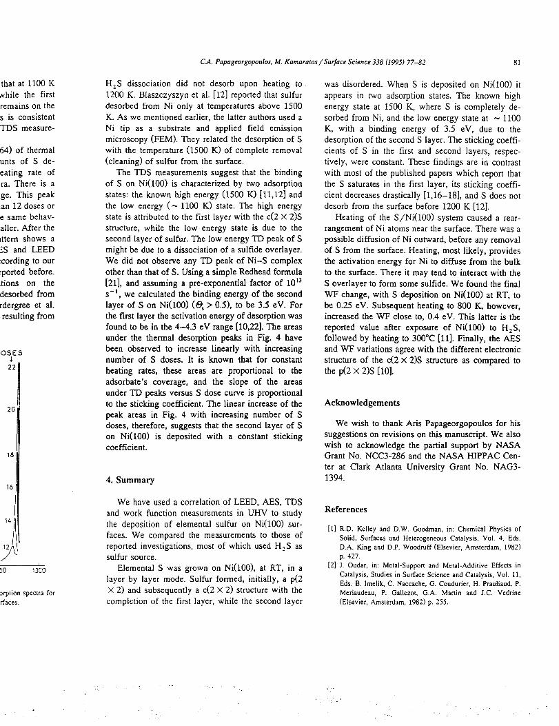
Fig. 3 shows the variation of the Auger peak-to-
peak height of the S(151 eV) and Ni(61 eV) peaks
and their ratio S(151 eV)/Ni(61 eV) of nearly twolayers of S covered the Ni(100) surface as a function
of substrate temperature up to 1100 K. The experi-
mental conditions did not allow us to go higher than
1150 K. As it is seen in this figure, the peak-to-peak
height of the S(151 eV) Auger peak remained almost
constant up to 1000 K. It started to decrease above
this temperature by about one tenth of its initial
height at 1100 K. The Ni(61 eV) peak-to-peak height,
however, increased almost linearly from the begin-ning of the heating. This increase became more
r :.
°/-
- L .
,%, . :

80 C,4. Papageorgopoulos, M. Kamaratos / Surface Science 338 (1995) 77-82
- -'"
,/
-t
1.5
"r"a. 1.0
x S(151 eV)
o Ni(61 eV)
• S/Ni
150
A
100
o
"r
5O
I i8ooT(K)
Fig. 3. Variation of the Auger peak-to-peak height of the S(151
eV), Ni(61 eV) peak and their ratio S(151 eV)/Ni(61 eV) of
nearly two layers of S covered the Ni(100) surface as a function
of substrate temperature up to 1100 K.
abrupt above 1000 K, where the S peak started todecrease. The S(151 eV)/Ni(61 eV) Auger ratio
decreased in proportion to the increase of the Ni(61
eV) peak. It appears that sulfur started to leave thesurface at about 1000 K. This is consistent with the
thermal desorption measurements shown in the next
figure. The unexpected continued increase of the
Ni(61 eV) peak from the beginning of the heating,when the S was not yet removed from the surface
may be attributed to a rearrangement of the surface.
Most likely, heating provides the activation energyfor the Ni atom to diffuse from the bulk to the
surface. The diffused Ni interacts with the S atoms,
possibly of the second layer, with the tendency to
form a disordered overlayer of a sulfide. The diffu-
sion should occur in a way that minimizes the mask-
ing of S atoms by the outgoing Ni atoms. The Satoms are smaller than those of Ni and diffusion of
the latter in between the S atoms of the c(2 × 2)S, in
the first layer, may cause an increase of the Ni Auger
peak height. The behavior of elemental sulfur on
Ni(100) is quite similar to that of O 2 on Ni(100).
Adsorption of oxygen on Ni(100) at RT forms a
c(2 × 2) with the completion of the first layer of
oxygen and then a thin film of Ni-oxide [20].
At 1100 K the S/Ni Auger peak-to-peak ratio is
reduced to about one, and the LEED pattern shows a
c(2 × 2) with sharp spots. This means that at 1100 K
the second layer of S is desorbed while the firstmonolayer with the c(2 × 2) structure remains on the
surface after heating to 1100 K. This is consistent
with the following correlation of the TDS measure-ments and LEED observations.
Fig. 4 shows a series of S 2 (amu 64) of thermal
desorption spectra for different amounts of S de-
posited on Ni(100) surfaces. The heating rate of
desorption was constant for all spectra. There is a
sharp peak in the 1050-1150 K range. This peak
appears only for S deposition higher than 12 doses or@s > 0.5. The S (amu 32) exhibits the same behav-
ior, but its TD peak is substantially smaller. After the
heating up to 1150 K the LEED pattern shows a
sharp c(2 × 2) as in the case of AES and LEED
correlation during heating (Fig. 3). According to our
knowledge, this peak has not been reported before.
Most of the experimental publications on theS/Ni(100) system report that sulfur desorbed from
Ni(100) at 1500 K. Specifically, Hardergree et al.
[11] report that the chemisorbed sulfur resulting from
...I<Z
t/'l
5-O
,ff
300 5_
= 20K/S
S DOS: S
22,
20
18
16
14
,2//
I I
800 I0 5O
T(K)
Fig. 4. A series of S 2 (amu 64) of thermal desorptton
different amounts of S deposited on Ni(100) surfaces.
I
1300
spectra for
C.A. Papageorgopoulos, M. Kamaratos / Surface Science 338 (1995) 77-82 81
that at 1100 K
Jchile the first
remains on the
s is consistent
TDS measure-
64) of thermalunts of S de-
eating rate ofra. There is a
ge. This peakan 12 doses or
e same behav-
aller. After the
tttern shows a
_.S and LEED
:cording to our
,,ported before.tions on the
desorbed from
rdergree et al.resulting from
OSE$
I
5O 1300
3rption spectra for
rfaces.
H2S dissociation did not desorb upon heating to
1200 K. Blaszczyszyn et al. [12] reported that sulfur
desorbed from Ni only at temperatures above 1500K. As we mentioned earlier, the latter authors used a
Ni tip as a substrate and applied field emission
microscopy (FEM). They related the desorption of S
with the temperature (1500 K) of complete removal
(cleaning) of sulfur from the surface.
The TDS measurements suggest that the binding
of S on Ni(100) is characterized by two adsorption
states: the known high energy (1500 K) [11,12] and
the low energy (_ 1100 K) state. The high energy
state is attributed to the first layer with the c(2 × 2)S
structure, while the low energy state is due to the
second layer of sulfur. The low energy TD peak of S
might be due to a dissociation of a sulfide overlayer.
We did not observe any TD peak of Ni-S complex
other than that of S. Using a simple Redhead formula
[21], and assuming a pre-exponential factor of 1013
s-t, we calculated the binding energy of the second
layer of S on Ni(100) (_s > 0.5), to be 3.5 eV. For
the first layer the activation energy of desorption was
found to be in the 4-4.3 eV range [10,22]. The areas
under the thermal desorption peaks in Fig. 4 have
been observed to increase linearly with increasingnumber of S doses. It is known that for constant
heating rates, these areas are proportional to the
adsorbate's coverage, and the slope of the areas
under TD peaks versus S dose curve is proportional
to the sticking coefficient. The linear increase of the
peak areas in Fig. 4 with increasing number of S
doses, therefore, suggests that the second layer of S
on Ni(100) is deposited with a constant stickingcoefficient.
4. Summary
was disordered. When S is deposited on Ni(100) it
appears in two adsorption states. The known high
energy state at 1500 K, where S is completely de-
sorbed from Ni, and the low energy state at ~ 1100
K, with a binding energy of 3.5 eV, due to the
desorption of the second S layer. The sticking coeffi-
cients of S in the first and second layers, respec-tively, were constant. These findings are in contrast
with most of the published papers which report that
the S saturates in the first layer, its sticking coeffi-
cient decreases drastically [1,16-18], and S does notdesorb from the surface before 1200 K [12].
Heating of the S/Ni(100) system caused a rear-
rangement of Ni atoms near the surface. There was a
possible diffusion of Ni outward, before any removal
of S from the surface. Heating, most likely, provides
the activation energy for Ni to diffuse from the bulk
to the surface. There it may tend to interact with the
S overlayer to form some sulfide. We found the final
WF change, with S deposition on Ni(100) at RT, to
be 0.25 eV. Subsequent heating to 800 K, however,increased the WF close to, 0.4 eV. This latter is the
reported value after exposure of Ni(100) to H2S,
followed by heating to 300°C [11]. Finally, the AES
and WF variations agree with the different electronic
structure of the c(2 X 2)S structure as compared tothe p(2 x 2)S [10].
Acknowledgements
We wish to thank Avis Papageorgopoulos for his
suggestions on revisions on this manuscript. We also
wish to acknowledge the partial support by NASAGrant No. NCC3-286 and the NASA HIPPAC Cen-
ter at Clark Atlanta University Grant No. NAG3-1394.
We have used a correlation of LEED, AES, TDS
and work function measurements in UHV to study
the deposition of elemental sulfur on Ni(100) sur-
faces. We compared the measurements to those of
reported investigations, most of which used H2S assulfur source.
Elemental S was grown on Ni(100), at RT, in a
layer by layer mode. Sulfur formed, initially, a p(2
X 2) and subsequently a c(2 X 2) structure with the
completion of the first layer, while the second layer
References
[I] R.D. Kelley and D.W. Goodman, in: Chemical Physics of
Solid, Surfaces and Heterogeneous Catalysis, Vol. 4, Eds.
D.A. King and D.P. Woodruff (Elsevier, Amsterdam, 1982)
p. 427.
[2] J. Oudar, in: Metal-Support and Metal-Additive Effects in
Catalysis, Studies in Surface Science and Catalysis, Vol. 11,
Eds. B. lmelik, C. Naccache, G. Coudurier, H. Prauliaud, P.
Meriaudeau, P. Gallezot, G.A. Martin and J.C. Vedrine
(Elsevier, Amsterdam, 1982) p. 255.
# .
82 C.A. Papageorgopoulos, M. Kamaratos / Surface Science 338 (1995) 77-82
•..:__'" _,_-_:' _i. :i
[3] J.M. MacLaren, J.B. Pendry, D.D. Vredensky and R.W.
Joyner, Surf. Sci. 162 (1985) 322.
[4] A.N. Maclnnes, M.B. Power and A.R. Barron, Chem. Mater•
4 (1992) 11.
[5] Ph.P. Jenkins, A.F. Hepp, M.B. Power, A.N. MacInnes and
A.R. Barton, Mater. Res. Soc. Syrup. Proc. 282 (1993) 111.
[6] M.P. Power, A.N. MacInnes, A. I-lepp and A.R. Barron,
Mater. Res. Soc. Syrup. Proc. 282 (1993) 660.
[7] R. McGrath, A.A. MacDowel, T. Hashizume, F. Sette and
P.H. Citrin, Phys. Rev. B 40 (1989) 9457.
[8] Th. Fauster, H. Durr and D. Hartwig, Surf. Sci. 178 (1986)
657.
[9] J.J. Barton, C.C. Bahr, S.W. Robey, Z. Hussain, E. Umbach
and D.A. Shirley, Phys. Rev. B 34 (1986) 3807.
[10] A. Patridge, G.J. Tatlock, FM. Leigsle, C.F.J. Flipse, F.
Hormandinger and J.B. Pendry, Phys. Rev. B 48 (1993)
8267.
[11] E.L. Hardergree, Pin Ho and J.M. White, Surf. Sci. 165
(1986) 488.
[12] M. Blaszcsyszyn, R. Blaszcsyszyn, R. Meclewski, A.J.
Melmed and T.E. Madey, Surf. Sci. 131 (1983) 433.
[13] L. Ruan, 1. Stengaard, F. Besenbacher and E. Laegsgaard,
Phys. Rev. Lett. 71 (1993) 2963.
[14] V. Starke, F. Bothe, W. Oed and K. Heinz., Surf. Sci. 232
(1990) 56.
[15] W. Oed, V. Starke, K. Heinz, K. Muller and J.B. Pendry,
Surf. Sci. 251/9,52 (1991) 488.
[16] T. Matsudaire, M. Nishijima and M. Onchi, Surf. Sci. 61
(1976) 651.
[17] S. Andersson, Surf. Sci. 59 (1979) 385.
[18] S. Andersson and J.B. Pendry, J. Phys. C 9 (1976) 2721.
[19] A.G. Baca, M.A. Shultz, D.A. Shultz and D.A. Shirley, J.
Chem. Phys. 81 (1984) 6304.
[20] C.A. Papageorgopoulos and J.M. Chen, Surf. Sci. 52 (1975)
53.
[21] P.A. Redhead, Vacuum 12 (1962) 203.
[22] S.R. Kelemen and T.E. Fisher, Surf. Sci. 87 (1979) 53.
•..7. --,.-._7!" _-__-.7_--" :-.-:
*:.

iELSEVIER Surface Science 352-354 (1996) 364-368
surface science
it_eund Theore-ersivit Bonn
ran.de
Adsorption of elemental S on Si(100)-2 × 1 surfaces
Ads Papageorgopoulos, M. Kamaratos * '_
Department of Physics and Center jor Higt Per/brmance Polymers and Ceramics, Clark Atlanta Unioersity, Atlanta, GA 30314, USA
Received 5 September 1995; accepted for publication 31 October 1995
_es, CA
aerque, NM1,W1Ly,NJa, TX
Barbara, CA
: Park, MD
"gh, PA
SSN 003%6028) are
times per month.)
Abstract
We have studied the adsowtion of elemental S on Si(100)-2 x 1 surfaces by LEED, AES. TDS, and WF measurements in
UHV. The adsorption of S at room temperature causes the surface restoration of the reconstructed Si(100)-2 X 1 substrate to
its original bulk-terminated surface, Si(100)-1 x 1. The S adsorbate follows the substrate structures, i.e. it forms initially a
(2 × 1) up to 0.5 ML and subsequently a (I × 1). Above I ML, sulfur is imbedded into the Si bulk near the surface. The
sticking coefficient of S on Si(I00) surface is constant, S = 1, up to 2 ML. Deposition of S at RT up to I ML increases the
WF of the surface by about 0.30 + 0.05 eV. Above I ML, as the S is diffused into the Si bulk, the WF decreases. The TDS
measurements show that S is desorbed as SiS molecule with a single TD peak near 585°C. This may indicate that the Si-S
hnnd energy is greater than that of Si-Si which may be the dominant cause of the substrate restoration.
Keyworas: Adsorption kinetics; Atom<;olid interactions, scattering, diffraction; Auger electron spectroscopy; Chemisorption; Low energy
electron diffraction (LEED); Low index single crystal surfaces; Semiconducting surfaces; Siliconl 3ulpbides; Surface electronic phenomena;
Thermal desorption spectroscopy; Work function measurements
1 request. A combineds 343-366, Applied
-face Science Reportsate. Subscriptions aresent by SAL (Surface
zailable. Airmail rates
dl enquiries regarding
98
ade within six months
V.. Molenwerf 1. P.O.
rth. Central and South
• 11003. Airfreight and
1. Introduction
Silicon as well as other semiconductors (GaAs,
InP) have demonstrated great value, along with their
importance in microelectronics and optoelectronics
[1,2], as sources of power (solar cells) for space
exploration [3].
The knowledge of the behavior of S alone on the
above semiconductors and specifically on Si is very
important because of the interest which has arisen
with respect to the possibility of pretreating the
surfaces of the semiconductors with S to protect and
stabilize these surfaces against degradation which
• Corresponding author. Fax: +30 651 45381.I Permanent address: Department of Physics, University of
loanntna, P.O. Box 1186, GR-451 10 [oannina, Greece.
may reduce their efficiency as solar cells or other
devices [4,5].
In addition to the importance in applications, there
is a recent rising scientific interest on the structural
and electronic properties of chalchogen elements (S,
Se) on Si(100)-2 × i surfaces. Theoretical calcula-
tions suggest that chalchogen adsorbates change the
structure of the Si(100)-2 X 1 surfaces [6,7]. Accord-
ing to our knowledge, this does not agree with the up
to-date relevant experimental results. More specifi-
cally, the Si(100) surface is easily reconstructed with
a small amount of heating. The clean Si(100) surface
shows a strong (2 x 1) reconstruction in the LEED
pattern. This has been observed for the first time by
Schlier and Farnsworth in 1959 [8]. It has been
recently accepted by most researchers that dimers are
the main building blocks of the reconstructed surface
0039-6028/96/$15.00 © 1996 Elsevier Science B.V. All fights reserved
SSDI 0039-6028(95)01161-7_ted in The Netherlands

rA Papa k'eorgopoulos, M, Kamaratos/'Surfiu'e Sctence 352-354 (1996) 364 368 365
of Si(100) [9]. The question, however, whether the
dimers are symmetric or buckled remains unclear, as
reported by Cbadi [10]. Today, new evidence ofasymmetric dimers is supported by most of the ex-
perimental [11-15] and theoretical [6,7] investigatorswho have '.vo:-Lzedon this p",:hl'_m. Kruger and Poll-
man [6] calculated that buckled dimers are energeti-
cally favored over symmetric ones by 0.14 eV per
dimer [6]. The restoration of reconstructed semicon-
ductor suriaces to their original bulk-terminated sur-
face has been achieved, lately, by different adsor-
bates other than S on Si (100) [16-19]. Adsorption
of S on clean Ge(100)-2 × 1 changed the (2 × l)
structure to (1 × 1). The system S/Ge(I × 1) was
regarded as an ideal terminated surface [20]. The
same authors [21] have. experimentally, investigated
the behavior of S on Si(100). They have not ob-
served an ordered S adlayer. Moriarty et al. [22]
reported, recently, that room temperature adsorption
of sulfur resulted in the formation of an overlayer
with the underlying Si(100) retaining the 2 X ' re-
construction. They also mentioned that annealing ofthe S/Si(100)-2 × 1 surface to 325°C leads to the
desorption of the sulfur overlayer and the appearance
of coexisting c(4 × 4) and (2 × 1) surface recon-
:<truction. In contraat to tlzis report, theoretical studiesperformed by Kaxiras ['/], and tater by Kruger and
Pollman [6], suggested that adsorption of group VIelements (S or Se) on Si(100)-2× 1 can lead to
restoration of the ideal bulk-terminated geometry onthe semiconductor surfaces. From the above discus-
sion it is apparently clear that additional effort on thestudy of S and Se on Si(100)-2 × 1 is necessary.
In this work we evaporate elemental sulfur on
Si(100)-2× 1 surfaces. The data suggest that the
presence of sulfur adsorbate on the surface changesthe surface structure of the Si(100)-2 × 1 substrate.
2. Experimental procedure
The experiments were performed in an ultrahigh
vacuum chamber (p < 10 -I° Ton'), equipped with a
cylindrical mirror analyzer (CMA) for AES measure-
ments, a quadrupole mass spectrometer (QMS) for
TDS measurements, a LEED system, and a Kelvinprobe for work function (WF) measurements.
Elemental sulfur was evaporated by thermal dis-
sociation of MoS 2 single crystal flakes mounted on a
tungsten filament. During dissociation of MoS 2 theMo remained on the tungsten filament, while S was
evaporated. The Si(lO0) substrate was cleaned byAr"- bombardment at E= 1 keV for 40 rain with an
ion current of 10 u,'_. After bombardment the sam-
pie was heated to 1000°C by passing current througha 0.05 mm Ta strip, uniformly pressed between the
sample and a Ta foil case. The temperature of the
sample was measured by a Cr-AI thermocouple. The
Si specimen was considered sufficiently clean when
the Auger peak height ratios C(272 eV)/Si(92 eV)and O(512 eV)/Si(92 eV) were below 1%. The
surface atomic density of I monolayer of S onSi(100) is considered equal to that of the outermost
layer of Si, Ns_ = 6.8 × 10 ''_ atoms cm -_.
3. Results
Fig. 1 shows the Auger peak-to-peak heights(Ap-pH) of the S(151 eV) and of the Si(92 eV) as a
function of the number of doses of S deposited on
clean Si(100)-2 ×1 surfaces at room temperature.These are in correlation with the observed LEED
patterns which will be discussed later in this section.
"i-]aeAuger peak-to-peak height of S(151 eV), as scc;_
in this figure, imtially increases linearly with an
increasing number ef S doses. Near the 9th dose the
curve forms a break (slope change of the S Augerpeak height versus S dose curve). The S Auger peak
height is increasing up to the 16th dose of ourmeasurements where it forms a second break. The
1.50
=eeo,-s
c_
&,<
• x
{Txl} _1-- (Ix]}
20MkX O.St, lt. tOl¢l. • I •
• • S (151 eV}xx • x ,_( 9'2ev}
X X• x x x x
, i
5
S / DOSES
2'O
Fig, I. Auger peak-to-peak heights of Si(92 eV) and S(151 eV)
versus S doses on clean Si(100)-2x I,

366 A. Papageorgopoulos, M. Kamaratos / Surface Science 352-354 (1996) 364-368
(2xl)
0.5
03
II (Ix})I
2OMt.O5,'_ IONt
y0.2
Ol
OD-o
e",,,- e __All__ o _.___. t
5 :O _5 2O
S / DOSES
Fig. 2. Work function change versus sulfur do:;es on Si( 100)-2 × 1
surface.
peak-to-peak height of Si(92 eV) decreases analo-
gously with a break occurring at about 8 doses of S.Above the 16th dose the S(151 eV) peal.: height
starts to level off, indicating that the sticking of S on
the Si surface becomes negligible. During S deposi-tion on the Si(100)-2 × 1 surface, the Auger Si(92
eV) peak is shifted with increasing number of Sdoses towards the lower energy by 1.5 eV up to the
16th dose of S. n_,'l-,_sis an indication of Si-S ;tronginteraction and will be digcussed further after the
TDS measurements.
Fig. 2 shows the work function (WF) changeversus the S doses on the clean Si(100)-2 × 1 surface
at room temperature. These measurements are also incorrelation with the LEED patterns during sulfur
deposition. The WF increases initially linearly withincreasing S coverage. Above the fourth S dose the
slope of the work function curve becomes smaller.Near the 9th dose, the work function reaches its
maximum value and subsequently starts to decreaseas the number of sulfur doses increases. Above the
thirteenth dose the decrease of the WF is very small,
despite that the Auger peak height of S(151 eV)continues to increase (Fig. 1).
Next we will combine the above measurements
with LEED observations. The clean Si(100)-2 ×1
surface shows a good, intense (2 × 1) LEED pattem.
Initial deposition of S on this surface does not
change the (2 × l) structure. Above the fourth dose,
the half-order spots become diffuse and the pattern
changes to a (1 × 1) with its maximum intensity near
the 9th dose. Further S deposition increases the
background, however, the (1 × 1) structure remains.We believe that S on Si(100)-2 × 1 forms also a
(2 × 1) structure, initially. The maximum intensity of
the (2 × 1) pattern, near the 4th S dose, corresponds
.,._,0.5 ML of S coverage. Above,the 4th_dose.,, ,b_th
the Si substrate and the S adsorbate change to a
(1 × 1) structure. The completion of the (1 × 1), near
the 9th dose, corresponds to 1.0 ML of S, and
coincides with the first break of the Auger curve
(Fig. 1) and the maximum increase of the WF value
(Fig. 2).
The same UHV system has been used previously
with the same S-source, and about the same flux of S
on Ni(100) [23]. The LEED observations showed the
formation of a c(2 × 2) pattern close to the 12th dose
of S on Ni(100). The density of the S overlayer,
which produces the c(2 × 2) on Ni(100) is 8 × 10¹⁴
atoms cm -2 at 12 doses. At 9 doses the densityshould be about 6 × 10 _'_ atoms cm -2. This is very
close to 6.8 × 10 _' atoms cm -2, which is the density
of 1 ML of S on Si(100). Therefore, the completionof the S(1 × 1) structure on Si(100) at 9 doses is
indeed about 1 ML of sulfur. It has been proposed
that the initial sticking coefficient of S on cleanNi(100) is close to unity [?4]. This implies that the
initial sticking coefficient of S on Si(100)-2 × 1 isalso one.
Thermal desorption spectra from S-covcredSi(100) surfaces did not show any observable peak
of S 2 (64 ainu). Sulfur was mainly desorbed as SiScompound. Fig. 3 shows a series of SiS (60 ainu) ol
thermal desorption spectra for different amounts of S
deposited on Si(100) surfaces. The heating rate otdesorption was constant, b = 30 K s --_, for all spec-
tra. There is only a single peak with its maximun"
value near 585°C. The areas under the TD peaks oI
SiS increase linearly with increasing number of S
doses up to 16th dose of S, where, we believe, tha_
the completion of the second S layer occurs. It b
known that the slope of the areas under the TD5
versus doses of a deposited adsorbate on a substrate
is proportional to the sticking coefficient of theadsorbate. This, implies that the sticking coefficien
of S on Si(100) surfaces is constant up to 2 ML, ant
subsequently becomes substantially smaller. Basec
on this we may assume that the drastic slope change:
near the 9th dose of the Auger curve (Fig. 1) and tht

A. Papageorgopoulos, M. Kamaratos / Surface Science 352-354 (1996) 364-368 367
._position increases the× 1) structure remains.
100)-2 x I forms also a
Lemaximum intensity of
4th S dose, corresponds
bo",. th;."4?., de,se, both
adsorbate change to a._tion of the (1 × 1), near
to 1.0 ML of S, and
ak of the Auger curve1crease of the WF value
as been used previouslyabout the same flux of S
observations showed the
rn close to the 12th dose
;ity of the S overlayer,) on Ni(100) is 8 × 10¹⁴
At 9 doses the density
:oms cm -2. This is very
a-2 which is the density
laerefore, the completion
n Si(100) at 9 doses is
ar. It has been proposed,efficient of S on clean
:4]. This implies that theA S on Si(100)-2 x 1 is
2_ S/Si(IO0)
13=30K/s
i
500 350 600 650
T (°C)
Fig. 3. Thermal desorption spectra of SiS from S-covered Si(100)
surfaces.
work function decrease (Fig. 2) are consistent with a
submergence of the second S layer into the Si nearthe surface.
During heating of the S-covered Si(100) surfacesthe Auger, LEED, and WF measurements follow
their variations during S deposition in reverse.
pectra from S-covered
Low any observable peak
; mainly desorbed as SiSseries of SiS (60 amu) of
'or different amounts of S
Lces. The heating rate of
= 30 K s -_ , for all spec-
4. Discussion
The current experimental LEED observations
show very clearly that deposition of elemental sulfuron clean Si(100)-2 × 1 surfaces at room temperature
changes the Si (100)-2 × 1 structure to Si(100)-I × 1.
This phase transition, is reported for the first time.
increasing number of S;, where, we believe, that
cmd S layer occurs. It is:he areas under the TDS
:1adsorbate on a substrate
icking coefficient of the
at the sticking coefficient
constant up to 2 ML, and
peak with its maximum i We believe that the S adsorbate follows the substrateas under the TD peaks of structures, i.e. it forms a (2 × I) up to 0.5 ML and a
(1 × 1) above this coverage.The TDS measurements (Fig. 3) show that S is
desorbed as SiS molecule. This indicates clearly that
the S-Si bond energy is greater than that of Si-Si,
which may indeed be the dominant cause of thesubstrate restoration to a Si(100)-I × 1. It is impor-
tant that the S coverage is greater than 0.5 ML inorder to maintain the Si restoration. Our results of S
9stantially smaller. Based adsorption on the Si substrate are in agreement with
t the drastic slope changes' Kaxiras [7], and later with Kruger and Pollman's [6]
ager curve (Fig. 1)and the I theoretical calculations. According to their results
adsorption of S or Se causes the surface restorationof the reconstructed Si(100)-2 × 1 substrate to its
original bulk-terminated surface. Kaxiras, in his re-
port, considered different structures consisting of
imbedding and mixing of the group-VI adatoms with
Si substrate atom._-_.This .is i,'._ agreement with the
imbedding of the second S layer into the Si bulk.
The author emphasizes, however, that the restored
surfaces are stable against all of the consideredalternative structures.
Besides the theoretical support [6,7] on therestoration of the semi-conductor surfaces to their
original bulk-terminated geometry achieved by S and
Se adsorbates, there are also several experimental
results mentioned already in the introduction. Espe-
cially, Weser et al. [20] reported that S on Ge(100)-2
X 1 changed the (2 × 1) structure to (1 × 1) and that
the S/Ge(100)-I ×1 system was regarded as anideal terminated surface. The same authors, however,
have not observed any ordered S overlayer on the
Si(100)-2 × 1 surface [21]. Recently, Moriarty et al.
[22] reported that room temperature adsorption of S
resulted in the formation of an overlayer on Si(100)-2 × 1, retaining the (2 × 1) reconstruction. They also
report that annealing of S covered Si(100)-2 × 1 at
325°C leads to the desorption of the sulfur overlayer
As it is already mentioned, the complete removal of
S takes place by heating the substrate to 650°C.
5. Summary
We have used a correlation of LEED, AES, TDSand work function (WF) measurements in UHV to
study the deposition of elemental sulfur on Si(100)-2
× I surfaces. The adsorption of S at room tempera-ture causes the gradual change of the reconstructedSi(100)-I × 1. The S adsorbate follows the substrate
structures, i.e. it forms initially a (2 × 1) up to 0.5
ML and subsequently a (1 × 1) structure. Above 1
ML, Sulfur is imbedded into the Si bulk near the
surface. The sticking coefficient of S on Si(100)
surface is constant, S = 1, up to 2 ML. Deposition of
S at RT up to I ML increases the WF of the surface
by about 30+0.05 eV. Above 1 ML, as the S isdiffused into the Si bulk, the WF decreases. TheTDS measurements show that S is desorbed as Si-S
molecule with a single TD peak near 585°C. This

368 A. Papageorgopoulos, M. Kamarato_ / Surfiace Science 352-354 _ 19961 364-368
may indicate that the Si-S bond energy is greater
than that of Si-Si which may be the dominant cause
of the substrate restoration.
Ackilowl_d_,,;ment.,
We wish to thank Professor C.A. Papageorgopou-
los, Director of the Surface Physics Laboratory, for
his help on the experiment and interpretation of this
work. We are also grateful to Adero Comer and
Dwight Mosby for their assistance. We acknowledge
the support of NASA Grant No. NCC3-286 and the
NASA High Performance Polymers and Cerarmcs
Center at Clark Atlanta University Grant No.
NAGW-2939.
References
[1] A.N. Maclnnes, M.B. Power and A.R. Barton Appl. Phys.
Lett. 62 (1993) 71I.
{2] R.R. Chang and D.L. Life, Appl. Phys. Lett. 53 (1988) 134.
[3] RK. Jain and G.A. Laundis, 22nd IEEE Photovoltaic Con-
ference. Las Vegas, USA (1991).
[4] 1. Weinberg, C.K. Swartz _md R.E. Hart', 18th IEEE Photo-
voltaic Specialists Conference, k,as Vegas, USA (!985).
[5] M.B. Power. A.N. Maclnnes, A.F. Hepp and A.R. Bah'on.
Mater. Res. Soc. Syrup. Proc. 282 (1993) 659.
[6] P. Kruger and J. Pollman. Phys. Rev. B 47 (1993) 1898.
[7] E. Kaxiras, Rapid Commun. Phys. Rev. B 43 (1991) 6824.
[8] R.E. Schlier and H.E. Famsworth. J. Chcm. Phys. 30 (1959
917.
[9] D.A. King and D.P. Woodruff, Eds., The Chemical Physic:
of Solid Surfaces and Heterogenous Catalysis, Vol. 5 (Else
vier, Amsterdam, 1988) p. 37.
[10] D.J. Chadi, Phys. Re','. Lett. 43 (1979) 43.
[1 !] R.M., _r_nar_ R.G. Smeenk and F.W. Saris. phys. Re..:_.I::,,46 (1981) 9392.
[12] M Aono, Y. Hou, C. Oshima and Y. Ishizawa, Phys. Re_
Lea. 49 (1982) 507.
[13] B.W. Holland, C.B. Duke and A. Paton, Surf. Sci. 14{
(1984) L269.
[14] R.J. Hamers, R.M. Tromp and J.E. Demuth, Phys. Rev. B 3.
(1986) 5343.
[15] R.A. Wolkow, Phys. Rev. Left. 68 (1992) 2636.
[16] R.D. Bringans, R.I.G. Uhrberg, R.Z. Bechrach and J.E
Northrup. Phys. Rev. Lett. 55 (1985) 533.
{17] R.D. Bringans, R.I.G. Uhrberg and R.Z. Beehrach, Phyr
Rev. B 34 (1986)2373.
[18] R.R.G. Uhrberg, R.D. Brigans. M.A. Olmstead, R.2
Brachrach and J.E. Northup. Phys. Rev. B 35 (1987) 394:
[19] R.D Schnell, F.J. Himpsel, A. Bogen, D. Rieger and
Steinmann, Phys. Rev. B (1985) 8052.
[20] T. Weser, A. Bogen. B. Konrad, R.D. Schnell. C.A. Schu_
W. Moritz and W. Steinmann, Sin;. Sci. 201 (1988) 245.
[21] T. Weser, A. Bogen, B. Konrad, R.D. Schnell, C.A. Schu
and W. Steinmann, Proc. 18th Int. Conf. on the Physics {
Semiconductors, Ed. O. Engstrom (World Scientific, Sing:
pore, 1987) p. 97.
[221 P. Moriarty, L. Koenders and G. Hughes. Phys. Re','. B ,_
(1993) t5950.
[23] C.A. Papageorgopoulos and M. Kamaratos, Surf Sci. 33
(1995) 77.
[24] M. Blaszczyszyn, R. Blaszczyszyn, Z. Medewski, A.
Melmed and J.E. Madey, Surf. Sci. 131 (1983) 433.
' ..'SP, O-fl PASSIVATION OF Si(100)2xl SURFACES WITH ELEM:ENTAL SULFUR _
"_..,_ ARIS PAPAGEORGOPOULOS @ _. "_
Department of Physics and Center for High Performance Polymers and Ceramics " --'-2._ "Ok--
Clark Atlanta University, Atlanta, GA 30314, USA %
ABSTRACT
Deposition of elemental S on S i(100)2x 1 surfaces at room temperature changes the
reconstructed Si(100)2x 1 to its original buN-terminated Si(100) 1x 1 surface. Sulfur forms initially
a (2xl) on the Si(100)2xl surface and subsequently a (lxl) on the Si(100)lxl. Above 1MI_,,
sulfur is diffused into the Si bulk near the surface. The sticking coefficient of S on Si(100) surface
is constant up to 2 lVlJ_,.Deposition of S at RT up to 1 ML increases the work function of the
surface by about .3+0.05 eV. Above 1 NIL, as the S is diffused into the Si bulk,the work
function decreases.
,r',
%
INTRODUCTION
Silicon and other semiconductors (GaAs, InP) are widely used in high-speed electronics,
long-wavelength optical circuits (optoelectronics) [1,2] and, mainly in space technology, as solar
cells (photovoltaics) [3]. Their efficiency, however, is reduced by radiation damage [4,5], and
other causes which may change the surface composition. To prevent damage in the surfaces
involved without reducing their efficiency the above semiconductors are pretreated with
protective films. Recently, an interest has arisen with respect to the possibility of pretreating the
surfaces of the above semiconductors with S and S-compounds to protect and stabilize them
against the degradation [4,5].Working on a program related to the growth of protective films on
photovoltaics, we felt that the knowledge of the behavior of S alone on the above
semiconductors and specifically on Si is very important.
In addition to the importance in applications, there is a recent rising scientific interest on the
structural and electronic properties of chalchogen elements (S,Se) on Si(100)2xl surfaces.
Theoretical calculations suggest that chalchogen adsorbates change the structure of the
Si(100)2xl surfaces [6,7]. According to our knowledge, this does not agree with the up to-date
relevant experimental results. It is well-known that the clean Si(100) surface shows a strong (2xl)
reconstruction in the LEED pattern. It has been recently accepted by most researchers that dimers
are the main building blocks of the reconstructed surface of Si(100) [6-14]. The restoration of
reconstructed semiconductor surfaces to their original bulk-terminated surface has been achieved,
lately, by different adsorbates other than S on Si(100) [15-18]. Adsorption of S on clean
Ge(100)2xl changed the (2xl) structure to (lxl). The system S/Ge(lxl) was regarded as an ideal
terminated surface[ 19]. The same authors[20] have, experimentally, investigated the behavior of S
on .Si(100). They have not observed an ordered S adlayer. Moriarty et al. reported, recently, that
room temperature adsorption of sulfur resulted in the formation of an overlayer with the
underlying Si(100) retaining the 2xl reconstruction [21]. They also reported that annealing of the
S/Si(100)2xl surface to 325°C leads to the desorption of the sulfur overlayer and the appearance
of coexisting c(4x4) and (2xl) surface reconstruction. In contrast to this report, theoretical
studies by Ka.,xiras [7], and later by Kruger and Pollman [6], suggested that adsorption of group
VI elements (S or Se) on Si(100)2xl can lead to restoration of the ideal bulk-terminated geometry
on the semiconductor surfaces. From the above discussion it is apparentJy clear that additional
effort on the study of S and Se on Si(100)2xl is necessary.

EXPERIMENT
Theexperimentwasperformedin anultra-highvacuumsystem(UHV) usinganAugerelectronspectrometer(AES), aquadrupolemassspectrometerfor TDS measurements,a lowenergyelectrondiffraction (LEED)system,anda Kelvin probefor work function(WF)measurements.Elementalsulfurwasevaporatedby thermaldissociationof MoS2singlecrystalflakesmountedona tungstenfilament. TheSi(100)substratewascleanedby At+ bombardmentatE = 1keV for 40min with anion currentof 10t.tA.After bombardmentthesamplewasheatedto 1000ocby passingcurrentthrougha0.05mmTa strip, uniformly pressedbetweenthesampleandaTa foil case.Thesurfaceatomicdensityof 1monolayerof SonSi(100)is consideredequalto that of theoutermostlayer of Si, NSi = 6.8x10¹⁴atoms'cm-2.
RESULTS
Fig. 1showstheAuger peaktopeakheights(Ap-pH) of theS(151eV) versusthe numberofSdosesdepositedoncleanSi(100)2xl surfacesatroomtemperatureandthesubsequentheatingtemperaturesof theSi substratefor 2 minutes.Thesemeasurementsareshownin correlationwith theobservedLEED patternswhichwill bediscussedlater in thissection.As seenin thisfigure,theAugerpeakto peakheightof S(151eV),initially increaseslinearlywith anincreasingnumberof S doses.Neartheninthdosethecurveformsabreak(slopechangeof theS Augerpeakheightvs S dosecurve).TheSAugerpeakheightis increasingupto theeighteenthdoseofourmeasurementswhereit formsasecondbreak.Above the 18th dosetheS(151eV)peakheightstartsto leveloff. With thesubsequentheatingtheS peakheightremainsnearlyconstantup to 400°C. Abovethis temperaturetheSpeakheightdecreasesdrastically,indicatingremovalof Sfrom thesurface,which iscompletedatabout650oc. During theS depositiontheenergyoftheSi Augerpeakis shiftedlinearlywith S dosesto lower energyby 1.5eV atthe18thdose(notshownhere).Thisis anAugerchemicalshiftwhichmaybeattributedto astrongbinding,probablycovalent,betweenS andSi.
Fig. 2 showsthework functionchange(k_) .versus.SdosesoncleanSi(100)2xl surfacesatroomtemperatureandthesubsequentheatingtemperaturesof theSi substratefor twominutes.During theS depositionatroomtemperature,thework functionincreasesinitially linearlywithincreasingS coverage.AbovethefourthSdosethework functioncurvedeviatesfrom linearityand itsslopebecomessmaller.Ne_ theninthdose,thework functionreachesitsmaximumvalue,andsubsequentlystartsto decreaseasthenumberof sulfurdosesincreases.Abovethethirteenthdosethedecreaseof thework functionis very small,despitethattheAugerpeakheightof S(151eV) continuesto increase.We shouldemphasizethatduringheatingthework functiondecreaseswhile theS Augerpeakheightremainnearlyunchangedup to300°C.Mostlikely,heatingprovidestheactivationenergyfor furtherdiffusionof S into thebulkof theSi substratecausingthework functiondecrease.Above400°Cthework functionincreaseswhile theAugerpeakof S decreasesdrastically,indicatingadrasticdesorptionof S from thesurface.At about550°C, the second S layer is removed completely and the work function increases to its maximum
value. Above 550oc, as the S coverage approaches the 0.5 NIL, the surface changes back to the
reconstructed (2xl). Near 650°C the S is completely desorbed from the Si substrate.
The LEED observations show that the clean Si(100)2xl surface gives a good intense (2xl)
LEED pattern. Above the fourth dose of S deposition on this surface, the half-order spots become
diffuse and the pattern changes to a (lxl) with its maximum intensity near the ninth dose. Further
S deposition increases the backgound, however, the (lxl) structure remains. It appears that

150 -
'T-
_ (2xl)too -
& •/
< •/
50 - /"
/
/
/
0!
(txl)
_L e,_.j.o, o --o-,
• "R _ 0"
/
(2x I)
G
/.0
\I 1 I "(
0 5 10 15 20 I I J I [ I -
0 200 400 600S/DOSES
T/oc
Figure 1. Auger peak to peak heights (Ap-pH) of the S(151 eV) versus
the S doses on clean Si(100)2xl surfaces at room temperature and
subsequent heating temperatures of the Si substrate for 2 minutes.
;>
e<1
0.6
0.5-(lxl)
;0.3-
0.2
O.I _-_'0.0
0 5 [0 15 20
S/DOSES
f I ff_I 1 I "0 200 400 600
T/oC
Figure 2 Work function change (A_) versus the S doses on clean
Si(100)2xi surfaces at room temperature and subsequent heating
temperatures of the Si substrate for two minutes.

abovethe4th doseof S theSi(lxl)2xl reconstructedsurfacechangesto aS(100)lxl. Webelievethatstructuraltendeficiesof theS adsorbateaccommodatesthechangeson theSisubstrate.Fig. 3 showsa sideview structuralmodelof (a) areconstructedSi(100)2xl surface(b) a (2xl) structureors (0.5ML) onSi(100)2xl (c) a (lxl) structureof S (1.0ML) onSi(100)lxl (d) a top(lxl) and adiffused(lxl) underla)er of S (-2.0 ML) onSi(100)Ixl. ( Pstandsfor thesurfacedipole moment).We proposein this figure that,SonSi(100)2xl formsalsoa (2xl) structure,initially. Themaximumintensityof the(2xl) pattern,nearthe4thdose,shouldcorrespondto 0.5 ML of Scoverage.Abovethe4th dose,boththeSi substrateandtheSadsorbatechangeto a(lxl) structure.Thecompletionof the(lxl), nearthe9thdose,correspondsto 1.0ML of S,andcoincideswith thefirst break of theAugercurveandthemaximumincreaseof thework functionvalue(Figs 1 and2). Abovethe9thdose,the(lxl) isretained.Despitethat theAugercurveremainslinearup to 9th S dose,thework functioncurvedeviatesfrom linearityat the4thdose.This maybeattributedto differentS sitesbeforeandafterthe4thdose.Assumingthatthebondingof S onSi is covalentup to 2 ML, thepolarizationoftheelectronicchargeof thedepositedSatomsremainsunchangedwith increasingcoverage.Therefore,anychangein dipolemomentshouldbeattributedto thedipolelengthchange.Consequently,theS atomson thedimersof theSi(100)2xl surfacemayhavegreaterdipolemomentP than onsiteson theSi(lxl) surfaces(Fig. 3). In the latter case, the distance between
the neighboring Si atoms of the top layer is greater than that between those of the dimers.
Therefore, the S adatoms should be deeper in their sites between the Si atoms of the (lxl)
surface structure, with a smaller dipole length and, therefore, smaller dipole length and work
function.. The fact that, above 1.0 ML (9th dose), the s!ope change of the Auger curve is rather
drastic (Fig. 1), as compared to cases of layer by layer growth [22], and the work function value
decreases may indicate that above 1.0 NIL the sulfur is submerged into the Si bulk near the
surface. The dipole moment of the submerged S atoms compensates that of the S overlayer with
a consequent lowering in work function (Fig. 2). Kaxiras, in his calculations [7], considered
different structures consisting of embedding and mixing of the group-VI adatoms with Si
substrate atoms. This is in agreement with our measurements which indicate an imbedding of the
second S layer into the Si bulk.
(a)
. °
o.
(c)
(b)
P,=P,-P.,
(d)
Figure 3 Side view of (a) a reconstructed Si(100)2x 1 surface (b) a (2x 1) structure of S
(0.5 ML) on Si(100)2xl (c) a (lxl) structure of S (1.0 NIL) on Si(100)lxl (d) a top (lxI)
and a diffused (Ixl) underlayder of S (-2.0 ML) on Si(100)lxl. ( P is dipole moment).

ThesameUHV systemhasbeenusedpreviouslywith thesameS-source,andaboutthesameflax of S onNi(100) [22]. TheLEED observationsshowedtheformationof ac(2x2)patterncloseto the 12thdoseof S onNi(100).Thedensityof theS overlayer,whichproducesthec(2x2)onNi(100), is 8x10¹⁴atoms'cm-2 at 12doses.At 9 dosesthisdensityshouldbeabout6x1014atoms.cm-2 . This is verycloseto 6.8x10¹⁴atoms.cm-2,which is thedensityof 1MLof S onSi(100).Therefore,at thecompletionof the(lxl) structureonSi(100),thecoverageofS at 9 dosesis indeedabout1ML. It hasbeenproposedthat the initial stickingcoefficientof SoncleanNi(100) iscloseto unity [23].This implies that the initial stickingcoefficientof S onSi(100)2xl is alsoone.Thelinearityof theAugercurve up to 1ML (Fig. l) indicatesthat thesticking coefficientof S onSi(100)surfaceremainsone,at least,up to 1ML. Theslopeof theAuger curve,however,is alsoconstantbetweenthefirst andthe secondbreak,whichoccursinaboutthesametime of thecompletionthef'mstmonolayer.This may furtherimply thatthestickingcoefficientof S is nearlyconstantup to the 18thdosewherethesecondlayer of S iscompleted.
CONCLUSIONS
The adsorption of S at room temperature causes the gradual change of the reconstructed
Si(100)2xl to its original bulk-terminated Si(100)lxl surface. The S adsorbate accommodates the
substrate" structural changes. Sulfur, at 0.5 ML, forms a (2xl) on the Si(100)2xl surface and
subsequently, at 1.0 ML, a (lxl) on the Si(100)lxl. Above 1 ML, sulfur is imbedded into the Si
bulk near the surface. The sticking coefficient of S on Si(100) surface is constant up to 2 ML.
Deposition of S at RT up to 1 ML increases the work function of the surface by about .3_+0.05
eV. Above 1 ML, as the S is diffused into the Si bulk, the work function decreases.
ACKNOWLEDGMENTS
I gratefully acknowledge the support of NASA Grant No. NCC3-286 and the NASA High
Performance Polymers and Ceramics Center at Clark Atlanta University Grant No. NAGW-
2939. I would also like to thank Adero Comer for his helpful assistance.
REFERENCES
1. A.N. MacInnes, M. B. Power, and A. R. Barton Appl. Phys. Lett., 62
(1993), 711.
2. R. R. Chang and D. L. Life, Appl. Phys. Lett., 53(2) (1988),134
3. R.K. Jain and G. A. Laundis, Twenty-Second IEEE Photovoltaic Conference,
Las Vegas NV, Oct. 7-11 (1991).
4. I. Weinberg, C. K. Swartz and R. E. Ha_if, Eighteenth EEE Photovoltaic
Specialists Conference, Las Vegas NV, Oct. 21-25 (1985).
5. M.B. Power, A. N. MacInnes, A. F. Hepp and A. R. BarTon, Mat. Res. Soc. Syrup.
Proc., 282 (1993), 659
6. Peter Kruger and Johannes Pollman, Phys. Rev. B 47 (1993), 1898.

7. Efthimios Kaxiras,RapidComm.Phys.Rev.B 43 (1991),6824..
8. The Chemical Physics Of Solid Surfaces and Heterogenous Catalysis, ed. D. A.
King and D. P. Woodruff, (Elsevier, Amsterdam, 1988),Voi.5, p.37.
9. D.J. Chadi, Phys. Rev. Lett., 43 (1979), 43.
10. R.M. Tromp, R. G. Smeenk and F. W. Saris, Phys. Rev. Lett., 46 (1981), 9392.
11. M. Aono, Y. Hou, C. Oshima and Y. Ishizawa, Phys. Rev. Lett., 49 (1982), 567.
12. B.W. Holland, C. B. Duke and A. Paton, Surf. Sci., 140 (1984), L 269.
13. R.J. Hamers, R. M. Tromp and J. E. Demuth, Phys. Rev. B 34 (1986), 5343.
14. R.A. Wolkow, Phys. Rev. Lett., 68 (1992), 2636.
15. R.D. Bringans, R. I. G. Uhrberg, R. Z. Bechrach and J. E. Northrup,
Phys.Rev.Lett., 55 (1985), 533.
16. R.D. Bringans, R. I. G. Uhrberg and R. Z. Bechrach, Phys. Rev. B 34 (1986),2373.
17. R.R.G. Uhrberg, R. D. Brigans, M. A. Olrmtead, R. Z. Brachrach and J. E. Northup,
Phys. Rev. B 35 (1987), 3945.
18. R.D. Schnell, F. J. Himpsel, A. Bogen, D. Rieger and W. Steinmann, Phys.Rev.
B (1985), 8052.
19. T. Weser, A. Bogen, B. Konrad, R. D. Schnell, C. A. Schug, W. Moritz and W.
Steinmann,Surf. Sci., 201 (1988), 245.
20. T. Weser, A. Bogen, B. Konrad, R. D. Schnell, C. A. Schug and W. Steinmann,
Procedings of the 18th ntemational Conference on the Physics of Semiconductors, ed. O.
Engstrom, (World Scientific, Singapore, 1987), p.97
21. P. Moriarty, L. Koenders and G. Hughes, Phys. Rev. B 47 (1993), 15950.
22. C.A. Papageorgopoulos, M. Kamaratos, Surf. Sci. 338, 77 (1995)
23. M. Blaszczyszyn, R. Blaszczyszyn, Z. Medewski, A. J. Melmed and J. E. Madey, Surf.
Sci., 131 (1983), 433.
Adsorption of elemental $ on Si(100)2x1:
Restoration
Surface c-_" _
A
.:.:.,- "'z.
Aris Papageorgopoulos and Adero Comer
Department of Physics and Center for High Performance Polymers and Ceramics
Clark Atlanta University, Atlanta, GA 30314, USA
M. Kamaratos and C. A. Papageorgopoulos
Department of Physics, University of Ioannina, P.O. Box 1186,
GR - 451 1 0 Ioannina, Greece
ABSTRACT
Adsorption of elemental S at RT causes the transition of the reconstructed
Si(100)2xl surface to its original bulk-terminated Si(100)lxl. The S adsorbate
forms initially a (2xl) structure at 0.5 MLs on the Si(100)2xl surface, a (lxl) at 1
ML on the Si(100)lxl, and above 1 ML sulfur is imbedded into the Si substrate. The
sticking coefficient of S is constant and equal to unity for the first 2 MLs.
Deposition of S at RT up to 1 ML increases the work function by 0.3+_0.05 eV. The S
adsorbate is strongly bound to the Si substrate in a molecular Si-S form. The Si-S
bond energy is greater than that of Si-Si, which may be the driving force of the
Si( 100)2x 1 --> Si(100) 1X1 transition.
2
I. INTRODUCTION
The passivation of semiconductor Surfacesis an area of intrinsic scientific
interest and of great technological importance. Silicon and other semiconductors,
such as GaAs and InP, are well-known for their potentially wide use in high-speed
electronics and long-wavelength optical circuits (optoelectronics) t,2. They have
also demonstrated great value, mainly in space technology, as solar cells
(photovoltaics) 3. Their efficiency, however, is reduced by electron 4, X-ray 5 and
gamma 6 radiation damage. Nonradiative recombination of charge carriers 1 is
another such cause. Moreover, interactions with surroundings such as oxidation
may cause a depletion, and generally a change of the surface composition. To
prevent damage in the surfaces involved without reducing their efficiency the above
semiconductors are passivated. This is done by depositing protective films
(dielectric window layers), such as chalcogenides: sulfur, gallium sulfide and indium
sulfide 7-10. Most of the studies concerning surface passivation of semiconductors
were carried out with the use of chemical vapor deposition techniques under
atmospheric pressure. The analysis of the deposited layers with the former
techniques has been obtained ex-situ after the completion of films a few hundred
nm's thick.
The in-situ analysis of the initial stages of the interface formation in ultra-
high vacuum (UHV) is necessary for the understanding and subsequent
improvement of the deposition process. The interface region between the
adsorbate and the substrate is that which primarily controls the growth of the films.
The understanding of the film growth, therefore, requires deposition methods that
allow control of the building process of the structure at the atomic level ll. A
beginning with elemental S deposition on Si(100)2xl in UHV would be appropriate.
The knowledge of the behavior of S alone on Si and other semiconductors is very
important because: (a)mf the interest which has arisen with respect to the
possibility of pretreating the surfaces of the semiconductors with S to protect and
stabilize these surfaces against degradation resulting in improved subsequent
processing 12,13, and (b) it will help to obtain a better understanding of the binding
structure and electronic properties of the growth of chalchogenide protective films
such as GaS and InS.
Besides the importance in applications, there is a recent rising scientific
interest on the structural and electronic properties of chalcogen elements (S,5e) on
Si(100)2xl surfaces. Theoretical calculations suggest that adsorbates change the
structure of the Si(100)2xl surfaces14,15. According to our knowledge, this does
not agree with the up todate relevant experimental results. More specifically, the
Si(100) surface is easily reconstructed with a small amount of heating. The surface
has a structure different from that of the bulk, and the reconstruction of the clean
surface occurs in order to reduce the number of broken dangling bonds 14. In other
words, the reconstruction of the surface drives to minimize the high energy of
broken covalent bonds, which would exist on an ideal bulkterminated plane IS. The
clean Si(100) deal bulk terminated plane 15. The clean Si(100) surface shows a
strong (2xl) reconstruction in the LEED pattern, observed for the first time by
5chlier and Farnsworth in 195916. Several models for the (2xl) reconstruction have
been proposed 17. It has been, recently, accepted by most researchers that dimers
are the main building blocks of the reconstructed surface of 5i(100). The question,
however, of whether the dimers are symmetric or buckled remains unclear, as
reported by Chadi 18. Today, new evidence of asymmetric (buckled) dimers is
supported by most of the experimental 19-23 and theoretical 14,15 investigators who
have worked on this problem. Kruger and Pollman 14 calculated that buckled
dimers are energetically favored over symmetric ones by 0.14 eV per dimer 14.
The restoration of reconstructed semiconductor surfaces to their original bulk-
terminated surface has been achieved, lately, by different adsorbates. Specifically,
ideal (lxl) terminations of (111) surfaces were reported for As on Ge(lll) 24 and
Si(ll 1)25,26 and for C1 omGe(111) 27. Adsorption of 5 on clean Ge(100)2xl changed
the (2xl) structure to (lxl). The system S/Ge(100)lxl was regarded as an ideally
terminated surface 28. The same authors 10 have experimentally investigated the
behavior of S on Si(100). They have not observedan orderedS adlayer. Moriarty
et al.30reported, recently, that room temperature adsorption of sulfur resulted in
the formation of an overlayer with the underlying Si(100) retaining the (2xl)
reconstruction. They also mentioned that annealingof the S/Si(100)2xl surfaceto
325 FC leads to the desorption of the sulfur overlayer and the appearance of
coexisting C(4x4) and (2xl) surface reconstruction. In contrast to this report,
theoretical studies performed by Kaxiras 15,and later by Kruger and Pollman14,
suggestedthat adsorptionof group VI elements(S or Se)on Si(100)2xl can lead to
the restoration of the ideal bulk-terminated geometry on the semiconductor
surfaces. From the abovediscussion it is apparently clear that additional effort on
the study of S and Se on Si(100)2xl is necessary.
Most of the sulfur adsorption studies, up to now have taken place with the
exposure of the substrates to H2S gas. To remove the H 2 from the surface the
substrates were heated to temperatures equal or greater than 200 oC. Hydrogen,
however, cannot be removed selectively. These mixed systems do not show any
well defined long range order 28. For a detailed understanding of the adsorption
kinetics of S on Si surfaces at room and lower temperatures, it is important to
deposit elemental sulfur.
In this work we evaporate elemental sulfur on Si(IO0)2X1 surfaces. We
study the sample using Low Energy Electron Diffraction (LEED), Auger Electron
Spectroscopy (AES), Thermal Desorption Spectroscopy (TDS),and Work Function
(WF) measurements. The data suggest that the presence of sulfur on the surface
causes a phase transition of the substrate. Preliminary results have been reported
in ECOSS and MRS 1995 Fall meetings.
II. EXPERIMENTAL
The experiments v_ere performed in an ultra-high vacuum chamber (p<10 -t°
Ton-), equipped with a cylindrical mirror analyzer (CMA) for AES measurements, a
quadrupole mass spectrometer (QMS) for TDS measurements, a LEED system,
and a Kelvin probe for WF measurements.
Elemental sulfur was evaporated by" thermal dissociation of MoS2 single
crystal flakesmounted on a tungstenfilament. During dissociationof MoS2 the Mo
remained on the tungstenfilament, while S was evaporated. The Si(100) substrate
was cleanedby Ar +bombardment at E=I keV for 40 min with an ion current of 10
mA. After bombardment the sample was heated to 1000oC by passing current
through a 0.05 mm Ta strip, uniformly pressedbetween the sample and a Ta foil
case.The temperature of the samplewas measuredby a Cr-AI thermocouple. The
Si specimenwas consideredsufficiently clean when the Auger peak height ratios
C(272eV)/Si(92eV) and0(512 eV)/Si(92eV) were below 1%. The estimation of the
S coverageson Si(100) surfaceswere basedon a correlation of LEED, AES and
TDS measurements, and the comparison with the measurements of S on the
Ni(100) surface which took place in the same system under the same deposition
conditions 31. The surface atomic density of 1 monolayer of S on Si(100) is
considered equal to that of the outermost layer of Si, Nsi=6.8xl014 atoms-cm -2.
III. RESULTS
Auger and Work Function measurements
Figure l shows the Auger peak to peak heights (Ap-pH) of the S(15 1 eV)
and the work function (A_) change as a function of the number of doses of S
deposited on clean Si(100)2xl surfaces at room temperature. These measurements
are shown in correlation with the observed LEED patterns which will be discussed
later in the next section. As seen in this figure, the Auger peak to peak height of S(
15 1 eV), initially increases linearly with an increasing number of S doses. Near the
ninth dose, the curve forms a break (slope change of the S Auger peak height vs S
dose curve). Also above _he 9th dose the S Auger peak height is increasing linearly
up to the eighteenth dose of our measurements where it forn-ls a second break.
Above the 18th dose the S(151 eV) peak height starts to level off. This Auger peak
' 6
• - ."S:'TZ'
. ,-Z..
height vs S doses curve is characteristic of a layer by layer growth. During the S
deposition on the clean Si(100)2xl surface at room temperature, the work function
initially increases linearly with increasing S coverage. Above the fourth S dose the
work function curve deviates from linearity and its slope becomes smaller. Near
the ninth dose, the work function reaches its maximum value, and subsequently
starts to decrease as the number of sulfur doses increases. Above the thirteenth
dose the decrease of the work function is very small, despite that the Auger peak
height of 5(15 1 eV) continues to increase. The maximum observed value of the
WF increase was about 0.3 eV. The above WF measurements were repeated three
times, and the maximum WF value varied by +0.05 eV. Fig. 2 shows the energy
shift of the integrated Auger Si(92 eV) peak during S deposition on clean
Si(100)2xl. The insert shows the Si(92 eV) energy shift versus S doses. According
to the insert, this shift increases linearly with increasing S doses to its final value of
1.5 eV at the completion of the second layer of S. During heating and as the S is
removed from the surface the shift decreases and the energy of the Si peak goes
back to that of the clean Si surface. This is an Auger chemical shift which may be
attributed to a strong S-Si interaction. Most likely, the S adatoms form a
compound with the Si substrate. The fact that the shift increases linearly may
indicate that the nature of binding is the same up to the completion of the second
layer, in agreement with the following TDS measurements.
TDS measurements
Thermal desorption spectra from S-covered Si(100) surfaces have shown
hardly observable peaks of S2 (amu 64). Sulfur was mainly desorbed as a SiS
compound. Fig. 3 shows a series of SiS (ainu 60) of thermal desorption spectra for
different amounts of St deposited on S(100) surfaces. The heating rate of
desorption was constant, b =20 K/s, for all spectra. There is only a single peak with
its maximum value near 585 °K, the very small peaks of S2, not shown here, appear
7
at the same temperature and probably are due to a partial dissociation of the SiS
molecule. This finding does not agree with Moriarty et al. 3o, who reported that the
annealing of the S covered Si(100)2xl surface to 325 oC leads to the desorption of
the sulfur overlayer. The latter disagreement will be also discussed in correlation
with other findings in the discussion. The fact that the TD peaks of SiS remain
relatively sharp at the same temperature with increasing S coverage indicates that
the nature of Si-S binding remains the same up to the completion of the S coverage
corresponding to the completion of 2 MLs, in agreement with the chemical shift
measurements.
Fig.4 shows the areas under the TD peaks of SiS (Fig. 3) versus the S doses
on Si(100) surfaces. Note that the S doses in the TDS were 15% greater than those
in the previous(AES and WF) measurements, and the completion of 2 ML's of S in
Fig. 4 occurs at the 1 5th dose. It is obvious, from this figure, that the TDS areas
increase linearly with increasing number of S doses, with a break (slope change of
the SiS TDS areas versus S doses curve) occurring near the 15th dose of 5, this is
where we believe that the completion of 2 ML's of sulfur takes place. It is known
that the slope of the areas under the TDS versus doses of a deposited adsorbate on
a substrate is proportional to the sticking coefficient of the adsorbate. This, in
correlation with Fig. 4, implies that the sticking coefficient of S on Si(100) surfaces
remains constant up to 2 MLs and subsequently becomes substantially smaller.
LEED measurements
The LEED observations show that the clean Si(100)2xl surface gives a good
intense (2xl) LEED pattern. Above the fourth dose of S deposition on this surface,
the half-order spots become diffused and the pattern changes to a (lxl) with its
maximum intensity near the ninth dose. Further S deposition increases the
background, however, the (lxl) structure remains. It appears that above the 4th
dose of S the Si(100)2xl reconstructed surface begins to change to a S(100)lxl. We
8
believe that S adsorption on Si(100)2xl forms also a (2xl) structure, initially. The
(2xl) pattern, near the 4th dose, should Correspond to 0.5 ML of S coverage.
Above the 4th dose, both the Si substrate and the S adsorbate change to a (lxl)
structure. The completion of the (lxl), near the the dose, corresponds to 1.0 ML
of S, and coincides with the first break of the Auger curve and the maximum
increase of the work function value (Fig. 1). Above the 9th S dose, the (lxl) is
retained.
The same UHV system has been used previously with the same Z-source,
and about the same flux of S on Ni(100) 31 The LEED observations showed the
formation of a c(2x2) pattern close to the 12th dose of S on Ni(100). The density of
the S overlayer, which produces the c(2x2) on Ni(100), is 8 x 10¹⁴ atoms.cm -2 at 12
doses. At 9 doses this density should be about 6 x 10¹⁴ atoms.cm -2 . This is very
close to 6.8 x 10¹⁴ atoms.cm -2, which is the density of 1 ML of S on Si(100).
Therefore, at the completion of the (lxl) structure on Si(100), the coverage of S at
9 doses is indeed about 1 ML. It has been proposed that the initial sticking
coefficient of S on clean Ni(100) is close to unity32. This implies that the initial
sticking coefficient of S on Si(100)2xl is also one. The linearity of the Auger curve
up to 1 ML (Fig. 1 ) indicates that the sticking coefficient of S on Si(100) surface
remains one, at least, up to 1 ML. The slope of the Auger curve is also constant
for the second monolayer, between the first and the second break, which occurs in
about the same time of completion as that of the first monolayer. This may
further imply that the sticking coefficient of S is nearly constant during the
adsorption of the second S layer, between the 9th and 18th doses. Moreover, the
TDS measurements (Fig. 4) indicate clearly that the sticking coefficient remains
constant and, therefore, equal to unity up to the completion of 2 MLs of S
coverage.
Despite that the ._uger curve remains linear and the sticking coefficient
remains constant up to 9th S dose, the work function curve deviates from linearity
at the 4th dose. This may be attributed to different sites of S atoms on Si before

9
and after the 4th dose. Both the chemical shift (Fig. 2) and the TDS (Fig. 4).
measurementsindicate that the nature of binding of S atoms on Si remains the
sameup to 2 MLs of S,which may imply that the chargetransfer (polarization) for
each5 adatom remainsalso the same. Therefore, any change to the surface dipole
moment should be attributed to the dipole length change. Consequently, the sulfur
atoms residing on the dimers of the 5i(100)2xl surface may have greater dipole
moment (dipole length) than on sites between Si atoms of the Si(lxl) surface. In
the latter case, the distance between the neighboring Si atoms of the top layer is
greater than that between those of the dimers of the reconstructed surface.
Therefore, the S adatoms should be deeper in their sites between the Si atoms of
the (lxl) surface structure, with a smaller dipole length, therefore, smaller dipole
moment and consequently a smaller work function than that for S atoms on the
dirners. This will be explained in more details in the discussion. The fact that,
above 1.0 ML (9th dose), the work function value decreases, while the sticking
coefficient and the nature of binding of S on Si remain constant, may indicate that
above 1.0 ML the sulfur is submerged into the Si bulk near the surface. Since the
WF lowering almost stops before the S coverage completion of 2 MLs means that
only part of the second layer is initially diffused into the bulk of Si at room
temperature.
Heating of S-covered Si(100)2xl surfaces
Fig. 5 shows the variation of the Auger peak to peak height (Ap-pH) of
S(151 eV) and the work function change (_X_), in correlation with the LEED
patterns, during the heating of the S-covered Si(100)2xl substrate. The heating was
implied in 50 °C increments for two minutes each. We should emphasize that the
work function decreases _ the early stages of the heating treatment and reaches its
minimum value at 300 oC, while the Auger peak height remains nearly unchanged
up to 400 oC i.e., at which the S is not yet removed from the surface. Most likely,

l0
heating provides the activation energy for diffusion of more S atoms into the bulk
of the Si substrate causing a further work function decrease. Above 400 oC, the
work function increases while the Auger peak of S decreases drastically, indicating a
drastic desorption of S from the surface. At about 550 °C, the second S layer is
removed completely and the work function increases to its maximum value of 1
ML. Above 550 oC the WF decreases again and as the S coverage approaches the
0.5 ML, the surface changes back to the reconstructed (2xl). Near
650 oC the S is completely desorbed from the Si substrate.
IV DISCUSSION
As we have mentioned previously, the current experimental LEED
observations show very clearly that deposition of elemental sulfur on clean
Si(100)2xl surfaces, at room temperature, changes the Si(100)2xl reconstructed
surface to a Si(100)lxl. This phase transition, is reported for the first time. We
believe that the S adatoms initially reside on the dimers forming a (2xl) at 0.5 ML
and a (lxl) above this coverage. In fig. 6 we propose a surface structural model of
sulfur on Si(100) surfaces. Fig. 6a shows a schematic side-view of the top three
layers of the clean reconstructed Si(100)2xl surface with the dangling bonds. The
deposited S atoms originally reside on bridge sites. Each S atom is specifically
bound through the dangling bonds on the two Si atoms of the dimer (fig. 6b), which
is consistent with the fact that S is divalent. The maximum coverage of this state is
0.5 ML at which all the climer sites are filled, and the S adatoms form a (2xl)
structure retaining the reconstruction of the Si substrate. This (2xl) structure of
the S overlayer on the Si(100)2xl surface has been named the hemisulfide state. As
the S deposition on the Si substrate continues above 0.5 MLs, the S atoms which
reside on available bridge sites between dimers cause the bonds between the Si
atoms of the dimers to Break, thus providing bonding for the S adatoms. As a
result of this process, the Si atoms are gradually displaced, causing the restoration
of the reconstructed Si(100)2xl to a Si(100)lxl surface. The sulfur aclatoms remain

11
. • -[
_':. Z..7 _
on the bridge sites, and are bound to neighboring Si atoms as it is shown in fig. 6c.
Thus, above 0.5 ME, S gradually forms a S(lxl) structure causing the change of the
Si substrate to an ideal bulk-terminated plane. This S(lxl) structure on Si(100)lxl
has been named the monosulfide state with a maximum coverage of 1 ME. Above
1 ME, S continues to be adsorbed with the same sticking coefficient up to the
coverage of 2 ML. Most of the 2nd monolayer of S is initially diffused into the bulk
of Si and later the diffusion decreases and Sremalns on the surface. The heating of
300 oC provides activation energy for further diffusion with a simultaneous
decrease of the WF. Fig. 6d shows a possible binding of the embedded S atoms
which we call disulfide state. Fig. 7 shows a top view of: (a) a clean Si(100)2xl
surface, Co) the hemisulfide on Si(100)2xl, (c) the monosulfide on Si(100)lxl and (d)
the disulfide on Si(100)lxl.
The break of the bond between the Si atoms of the dimers and the
subsequent rearrangement to a (lxl) structure is consistent with a strong Si-S
interaction. This strong interaction is suggested by the chemical shift of the Auger
Si(92 eV) peak during S deposition (fig. 2) and the TDS measurements (fig. 3). the
latter measurements show that the S is desorbed as a SiS molecule, indicating
clearly that the Si-S bond energy is greater than that of Si-Si, which may indeed be
the dominant cause of the substrate restoration to a Si(100)lxl. The greater S-Si
bond energy than that of Si-Si substrate has been reported some time ago 33. The
heating results (fig. 5) indicate that, as soon as part of the S is desorbed from the
surface and the coverage is < 0.5 ML the reconstructed (2xl) comes back again.
Our model of S adsorption on the Si substrate is in agreement with Kaxiras'15, and
later with Kruger and Pollman's 16 theoretical calculations. According to their
results adsorption of S or Se causes the surface restoration of the reconstructed
Si(100)2xl substrate to its original bulk terminated surface. Kaxiras, in his report,
considered different strucl-ures consisting of embedding and mixing of the group-VI
adatoms with Si substrate atoms. He emphasizes, however, that the restored
surfaces are stable against all of the considered alternative structures. This in
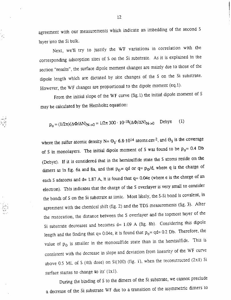
,. ,--.j
°
12
agreement with our measurements which indicate an imbedding of the second S
layer into the Si bulk.
Next, we'll try to justify the WF variations in correlation with the
corresponding adsorption sites of S on the Si substrate. As it is explained in the
section "results", the surface dipole moment changes are mainly due to those of the
dipole length which are dictated by site changes of the S on the Si substrate.
However, the WF changes are proportional to the dipole moment (eq.1).
From the inRial slope of the WF curve (fig. I) the initial dipole moment of S
may be calculated by the Hemholtz equation:
Po = (1/2r0(AcP/AN)N->0 = 1/2re 300- 10-18(A¢/AN)N_>0 Debye (1)
7 . "
!/?_
where the sulfur atomic density N= O s. 6.8-1014 atoms.cm -2, and ®s is the coverage
of S in monolayers. The initial dipole moment of S was found to be po = 0.4 Db
(Debye). If it is considered that in the hemisulfide state the S atoms reside on the
dimers as in fig. 6a and 8a, and that po = qd or q= Po/d, where q is the charge of
each S adatoms and d= 1.87 A, it is found that q= 0.04e (where e is the charge of an
electron). This indicates that the charge of the S overlayer is very small to consider
the bonds of S on the Si substrate as ionic. Most likely, the S-Si bond is covalent, in
agreement with the chemical shift (fig. 2) and the TDS measurements (fig. 3). After
the restoration, the distance between the S overlayer and the topmost layer of the
Si substrate decreases and becomes d= 1.09 A (fig. 8b). Considering this dipole
length and the finding that q= 0.04e, it is found that po = qd= 0.2 Db. Therefore, the
value of Po is smaller in the monosulfide state than in the hemisulfide. This is
consistent with the decrease in slope and deviation from linearity of the WF curve
above 0.5 ML of S (4th dose) on Si(100) (fig. I), when the reconstructed (2xl) Si
surface startes to change lo its' (lxl).
During the binding of S to the dimers of the Si substrate, we cannot preclude
a decrease of the Si substrate WF due to a transition of the asymmetric dimers to
13
their symmetric arrangement. It has already been mentioned in the introduction
the existing view that the dimers of the Si(100) are buckled. This asymmetric
deformation increases the dipole moment of the dimers, and the WF is greater
than that of the substrate with unbuckled (symmetric) dimers 1 8, 34 The existence
of the asymmetric dimers is supported experimentally by ion scattering 19, 20 and
LEED experiments 21. Recent STM 22, 23 measurements and theoretical calculations
14, 15 make the view of asymmetric dimers even stronger. From our
measurements it is not clear that the dimers remain asymmetric in the hemisulfide
state or that during S deposition the asymmetric dimers change to symmetric. In
the latter case, the increase of the work function during S deposition in the
hemisulfide state would be compensated to some degree by the WF lowering
during the transition of the asymmetric dimers to their symmetric state. The
increase of the WF in the hemisulfide state ,however, was very close to 0.25 eV
measured (in the same UHV system) for 0.5 ML of S on Ni(lO0) 31 surface, which
may indicate that the increase in WF up to 0.5 ML was due to the adsorption of S
alone and not to any structural change of the dimers.
Besides the theoretical support 14, 15 on the restoration of the
semiconductor surfaces to their original bulk-terminated geometry achieved by S
and Se adsorbates, there are also several experimental results mentioned in the
introduction. These results, however, refer to As on Ge(lll) 24 and on Si(ll 1)25,
26, and to C1 on Ge(lll) 27 Weser et al 28 reported that S on Ge(100)2xl changed
the (2xl) structure to (lxl) and that the S/Ge(100)lxl system was regarded as an
ideal terminated surface. The same authors, however, have not observed any S
overlayer on the Si(100)2xl surface 29. Recently, Moriarty et al 30 reported that
room temperature adsorption of S resulted in the formation of an overlayer on
Si(100)2xl, retaining the (2xl) reconstruction. They also report that annealing of S
covered Si(100)2xl at 325 FC leads to the desorption of the sulfur overlayer. As it
is already mentioned, the complete removal of S takes place by heating the
substrate to 650 FC. The same authors, in continuing their investigation,
7_ _ 7-.
• :'9
14
discovered coexisting c(4x4) and (2x l) surface reconstructions after the desorption
of S at 325 FC. Our finding that S is desorbed as SiS molecule show that heating
causes depletion of Si from the surface. Annealing at relatively low temperatures
would cause a partial removal of Si from the surface which could change the
reconstruction from (2xl) to a c(4x4). Although our structural models are
consistent with the experimental results, we cannot rule out completely the
possibility that, from the beginning of deposition, S forms 2D-islands of (lxl).
Above a certain coverage, the islands coalesce leading to a uniform (ix1) structure
at 1 ML. More work is needed to be done.
V. CONCLUSION
The adsorption of elemental S at room temperature causes the change of
the reconstructed Si(00)2xl substrate to its original bulk-terminated Si(100)lxl
surface. The S adsorbate forms initially a (2xl) stucture at 0.5 ML on the
Si(100)2xl substrate and subsequently a (lxl) on the Si(100)lxl. Above 1 ML,
sulfur is imbedded into the Si bulk near the surface. The sticking coefficient of S on
Si(100)2xl surface is constant and equal to unity for the first 2 MLs. Deposition of
S at RT up to 1 ML increases the work function of the surface by about 0.3+0.05 eV.
Above 1 ML, as the sulfur is diffused into the Si bulk, the work function decreases.
Surface dipole moment estimations based on the work function measurements
suggest that the Si-S bond is covalent. The deposition of S causes a chemical shift
of the Si(92 eV) peak of 1.5 eV, indicating a strong S-Si interaction. While the TDS
measurements show that S is mainly desorbed in the form of SiS compound. This
result supports the argument that the Si-S bond energy is greater than that of Si-Si,
which may be the driving force of the Si(100)2xl --> Si(100)lxl transition.
Acknowledgements-Th, authors wish to acknowledge the support of the NASA
Grant No. NCC3-286 and the NASA High Performance Polymers and Ceramics
Center at Clark Atlanta University Grant No. NAGW-2939.
15
REFERENCES
1A. N. MacInnes, M. B. Power, and A. R. Barron Appl. Phys. Lett. 62, 711 (1993).
2R. R. Chang and D. L. Life, Appl. Phys. Lett. 53(2), 134 (1988).
3 R. K. Jain and O. A. Laundis, Twenty-Second IEEE Photovoltalc Conference, Las
Vegas, NV, Oct. 7-11 (1991).
4 M. Yamaguchi et al., Appl. Phys. Lett. 44,432 (1984).
5 A. Yamamoto, M. Yamaguchi and C. Vemura, Appl. Phys. Lett. 44,611 (1984).
6 I. Weinberg, C. K. Swartz and R. E. Harf, Eighteenth IEEE Photovoltaic
Specialists Conference, Las Vegas NV, Oct. 21-25 (1985).
7 R. Leonelli, C. S. Sundaraman, 1. F. Currie, Appl. Phys. Lett. 57, 2678 (1990).
8 5. Shikoda, H. Okada, H. Hayashi, J. Appl. Phys. 69, 2717 (1991).
9 A. N. MacInnes, M. B. Power and A. P. Barron, Chem. Mater. 4, I1 (1992).
10 M. B. Power, A. N. MacInnes, A. F. Hepp and A. R. Ban-on, Mat. Res. Soc.
Symp. Proc. 282, 659 (1993).
11 A. Madhukar, Thin Solid Films 231, 8 (1993).
12 K. P. Pantie and D. Gutierrez, Appl. Phys. Lett. 46,416 (1985).
13 j. Chare, A. Choujaia, C. Santinelli, R. Blanchef and P. Victorovitch, J. Appl.
Phys. 61,257 (1987).
14 Peter Kruger and Johannes PoUman, Phys. Rev. B 47, 1898 (1993).
15 Efthimios Kaxiras, Rapid Comm. Phys. Rev. B 43,6824 (1991).
t6 R. E. Schlier and H. E. Farnsworth, J. Chem. Phys. 30,917 (1959).
17 The Chemical Physics Of Solid Surfaces and Heterogenous catalysis, ed. D. A.
King and D. P.Woodruff, Vol. 5, p.37, (Elsevier, Amsterdam, 1988).
t8 D. J. Chadi, Phys. Rev. Left. 43, 43 (1979).
19 R. M. Tromp, R. G. Smeenk and F. W. Saris, Phys. Rev. Left. 46, 9392 (1981).
20 M. Aono, Y. Hou, C. qsh na and Y. Ishizawa, Phys. Rev. Lett. 49,567 (1982).
21 B. W. Holland, C. B. Duke and A. Paton, Surf. Sci. 140, L 269 (1984).
22 R. J. Hamers, R. M. Tromp and J. E. Demuth, Phys. Rev. B 34, 5343 (1986).

16
23 R. A. Wolkow, Phys. Rev. Lett. 68, 2636 (1992).
24 R. D. Bringans, R. I. G. Uhrberg, R. Z. Bechrach and J. E. Northrup, Phys. Rev.
Lett. 55, 533 (1985)
25 R. D. Bringans, R. I. G. Uhrberg and R. Z. Bechrach, Phys. Rev. B 34, 2373
(1986).
26 R. R. G. Uhrberg, R. D. Brigans, M. A. Olmstead, R. Z. Brachrach and J. E.
Northup, Phys. Rev. B 35, 3945 (1987).
27 R. D. Schnell, F. J. Himpsel, A. Bogen, D. Rieger and W. Steinmann, Phys. Rev. B
32, 8052 (1985).
28 T. Weser, A. Bogen, B. Konrad, R. D. Schnell, C. A. Schug, W. Moritz and W.
Steinmann, Surf. Sci. 201,245 (1988).
29 T. Weser, A. Bogen, B. Konrad, R. D. Schnell, C. A. Schug and W. Steinmann,
Procedings of the 18th nternational Conference on the Physics of
Semiconductors, ed. O. Engstrom, p.97 (World Scientific, Singapore, 1987).
30 p. Moriarty, L. Koenders and G. Hughes, Phys. Rev. B 47, 15950 (1993).
31 C. A.Papageorgopoulos and M. Kamaratos, Surf. Sci. 338, 77 (1995)
32 M. Blaszczyszyn, R. Blaszczyszyn, Z. Medewski, A. J. Melmed and J. Madey,
Surf. Sci. 131, 433 (1983).
33 M. Copel, M. C. Reuter, E. Kaxtras and R. M. Tromp, Phys. Rev. Lett. 63,632
(1989).
34 Woodruff and T. A. Delchar, Modem Techniques of Surface Science, Cambridge
University Press, Cambridge, GB, 1986.

17
FIGURE CAPTION
Figure 1. Auger peak to peak heights (Ap-pH) of the 5(151 eV) and the work
function (A,) change as function of the number of doses of S
depositedon clean 5i(100)2xl surfacesat room temperature
Figure 2. Energy shift of the integrated Auger Si(92 eV) peak during S
depositionon cleanSi(100)2xl. The insert showsthe Si chemicalshift
versusS doses.
Figure 3.
Figure4.
Thermal desorption spectra of SiSfrom S-coveredSi(100)surfaces.
Areas under the thermal desorption peaks of SiS (Fig. 3) and S2
versusS doseson Si(100)surfaces.
Figure5. Variation of the Auger peak to peak height (Ap-pH) of 5(151 eV)
and the work function change (A_) during the heating of the S-
covered Si(100)2x 1 surfaces.
Figure 6. Side-view schematics of (a) the top three layers of clean
reconstructed Si(100)2xl surface with the dangling bonds, (b) the S-
(2xl) (hemisulfide) structure on the 5i(100)2xl surface, (c) the S-
(lxl) (monosulfide) structure on Si(100)lxl surface, and (d) the
diffused second S layer into the bulk of Si(100)lxl.
Figure 7.
Figure 8.
Top-view schematics of (a) the top three layers of the clean
reconstructed Si(100)2xl surface, (b) the S-(2xl) structure on the
Si(100)2xl surface (c) the S-(IxI) structure on Si(100)lxl surface and
(d) the diIfutsed second S layer into the bulk of Si(100)lxl.
Location of the S atoms (a) on the Si(100)2xl surface, (b) on the
Si(100)lxl surface.

(AO) ,I,V
\
\
\
.0
(slIun "qag) Hd-dv
r_
0
r_

o_
Z;
0
S DOSES
5 10 15
S DOSES
0
1
2
] 46
13
15
Auger Chem _" 17
Shift of Si (92 eV) 1.5 ev \19
75
! ! I I
79 83 87 91 95
E (eV)

¢lU
e_
r_
500
25 S/Si(100)
[I-3"0K/s
600I
650
T (°C)

tfb
| I
S(II S!S
0
0
0
Lr_
0
@
7

rJl
olil
|
<
150
100
50
0
1.0
o WF (DF)
x Si (92 eV)
,5 S (151 eV)
•A_A _A _A
.* (lxl)
i
×
0 100 200 300 400 500 600 700
0.8
0.6
0.4
0.2
0.1
8OO
T/oc

J_
.{.
®
_S

@O@O@@o@o@@0@[email protected].@o0o@@0@0@@0000@0@0@
OQO@o0o0
QO@O@ ,00000+@0@0@00000@0@0@
..
k
;>
Q @ @
@ © ©@ @@ © ©

Si Si
(a) S/Si (100) 2xl
o1._ A
Si Si Si Si
(b) S/Si (100) Ixl

Adsorption of Cs on S - covered Si(lO0) surfaces
Aris Papageorgopoulos, D. C. Papageorgopoulos*
Department of Physics, Clark Atlanta University.
James P. Brawley Drive at Fair Street S. W., Atlanta, GA 30314,
Abstract
This paper describes the adsorption of Cs on clean Si(100)2xl, on 0.5 MLs of
S- covered Si(100)2xl, and on 1 ML of S-covered Si(100)Ixl surfaces at RT. This is
based on our recent report that adsorption of elemental sulfur above 0.5 MLs on clean
Si(100)2xl causes the change of the reconstructed Si(100)2xl to a Si(100)lxl surface.
The investigation takes place in ultra high vacuum (UHV) system with Auger electron
spectroscopy (AES) and work function (WF) measurements. The saturation coverage of
Cs on clean Si(100)2xl surface at RT is 1ML. The presence ofpredeposited S on the
Si(100)2xl surface increases the binding energy and the maximum amount of Cs that can
be deposited on the Si(100) surface at RT. Adsorption of Cs on clean Si(100)2xl gives
the characteristic work function curve of alkali on metals and most semiconductors, i.e. an
initial minimum and subsequent increase towards the value of metallic Cs. Preadsorption
of S on Si(100)2xl further lowers the WF during subsequent Cs deposition by about 4 eV
to a plateau without the final increase which characteristic of the overlayer's metalization.
This is consistent with a covalent bonding of S with the Si substrate. The stable minimum
WF value of Cs on the S-covered Si(100)lxl surfaces might be very interesting for low
work function devices (cathods, energy converters).
Keywords: Auger electron spectroscopy; Work function measurements; Silicon; Cesium;
Sulfur.
I. Introduction
The adsorption of alkali on semiconducting substrates is an area of scientific
interest and great technological importance. Alkali-semiconductor interfaces are also very
important for understanding interracial metallization and Schottky barrier formation [ 1 ].
Special effort has been given to alkali adsorption on Si(100) surfaces. It has been
proposed first by Levin [2 ] and then later by others [ 1, 3- 6] that alkali, and specifically
Cs adatoms forming one-dimensional chains, reside on the raised sites of dimers of clean
Si(100)2xl [ 1,3 - 6 ]. Spiess et al. [ 7 ] support the one-dimensional chain for Na on
Si(100)2xl, but they consider Na atoms only to be adsorbed on the cave sites. Recently, a
double-layer model has been proposed by Abukawa and Kono [ 8 ], where the alkali

(cavesiteor valleybridgesite),andprovidea saturationcoverageof of onemonolayer,®= 1.Thesurfaceatomicdensityof 1monolayerof CsonSi(100)2xl isconsideredequaltothatof theoutermostlayerof Si,Nsi = 6.8xl 0TMatoms, cm-L The adsorptio of alkali on
most metallic and semiconducting surfaces causes a decrease in work function which
is interest in the making of thermionic energy converters [ 9 - 11 ]. The coadsorption of
the electropositive alkali and elect®negative elements, such as oxygen, decreases further
the work function of the surface and thus increasing the effciency of the thermionic
emission of electrons. The sulfure is also an electronegative element and we thought that
coadsorption of Cs ane S2 on Si(100)2xl would be interesting. This thought is favored by
the recent important finding when elemental sulfur was deposited on clean the Si(100)2xl
surface [ 12]. Briefly, adsorption of elemental S at RT causes the transition of the
reconstructed Si(100)2xl surface to its original bulk-terminated Si(100)lxl. This
transition takes place when ®s > 0.5 MLs. Above 1 ML sulfur is imbedded into the Si
crystal. The S adsorbate is strongly bound to the Si substrate in a molecular Si-S form.
We believe that Cs on a Si (100)2xl surfaces passivated with S, may help the growth of
Cs films greater than the single layer and reduce the work function of Cs on Si(100)2xlfurther.
It is possible to control growth at the atomic level in certain systems with the proper
choice of components and processing methods. The restoration of semiconductor surfaces
to their original bulk-terminated surface has been achieved for different adsorbates.
Specifically, ideal (lxI) terminations of(111) surface were reported for As on Si(l 11)
[ 13, 14 ]. Moreover, a monolayer of As was used to successfully control the growth of the
Ge overlayer on Si substrates [ 15]. When Ge is deposited on clean Si(100) it grows
epitaxially for three monolayers, but then reverts to island growth. This is due to the
lattice mismatch and the balance of surface and interface energies. A monolayer of As
passivates the Si(100) surface. Arsenic keeps floating on top of the Ge during growth,
allowing the pseudomorphic growth of considerably thicker Ge films, up to at least fifteen
monolayers (15 MLs). More recently, group III atoms were used as surfactants during the
growth of Ge on Si(111) [16]. The surfactants produce large changes in the surface
energy of the Si surfaces.
In this work the adsorption of Cs on S-covered Si(100)2xl surfaces is investigated. The
properties of the above surface system has been studied using Auger electron
spectroscopy (AES) and work function (WF) measurements. The kinetics and the mutual
effects of Cs and S during their coadsorption on Si(100)2xl have been discussed and are
reported for the first time.
II. Experimental
The experiments were performed in an ultra-high vacuum (UHV) chamber (p < 10-1°
torr), equipped with a cylindrical mirror analyzer (CMA) for AES measurements and a
Kelvin probe for WF measurements, the Si(100) substrate was cleaned by Ar+bombardment at E = 1 keV for 40 min with an ion current of 10 mA. After bombardment
the sample was heated to 1000 oC by passing current through a 0.05 mm Ta strip,

uniformlypressedbetweenthesampleandaTa foil case. The specimen temperature T s
was measured with a chromel-alumel thermocouple, spot welded onto the sample holder.
Elemental sulfur was deposited by thermal dissociation of MoS 2 single crystal flakes
mounted on a tungsten filament. During dissociation ofMoS 2 the Mo remained on the
tungsten filament while S was evaporated. The pressure was kept on the order of 10-_°
torr as the S was deposited on the surface. The Cs deposition was done using a
conventional alkali Getter source. The estimation of the S coverages on Si(100) surfaces
were based on the reported results [ 12] in correlation with our AES and work function (
WF ) measurements.
III. Results-Discussion
Auger measurements
As it is mentioned in the introduction, during deposition of S up to 0.5 MLs the
recostructed S(100)2xl surface is remained , whereas, with increasing S coverage
above 0.5 ML the surface changes to a S(100)lxl [12]. Based on this information we
measure the Auger peak to peak hight of Cs( 47 eV ) versus Cs deposition doses on 0.5
MLs of S- covered Si(100)2xl and on 1 ML of S- covered Si(100)txl, as compared to
that of Cs on clean Si(100)2xl, shown in Fig. 1.The Auger peak to peak height (Ap-pH)
of Cs, at first, increases linearly up to the third dose of Cs. Between the third and fourth
dose the slope of the Ap-pH vs Cs dose-curve decreases substantially. The new slope is
nearly constant up to the ninth dose, where the Auger curve levels off, and the Cs
coverage is saturated. We believe that at ninth dose the Cs saturates with a coverage of 1
ML ( which has a density equal to the outermost layer of Si substrate ). The break near
the fourth dose is attributed to different sites occupied by the Cs atoms before and after
the break. Specifically, the Cs atoms are initially adsorbed on the dimer sites. After the
completion of these sites, at fourth dose, the Cs atoms reside on the trough sites between
the dimer rows. This is consistent with the double-layer model proposed by Abukawa and
Kono (8). When Cs is deposited on S-covered Si surfaces, the Cs Auger peak heighr
continues to increas up to our last measuremert, in contrast to that on clean Si surface
which levels offnear the completion of the first monolayer..A comparison of the Auger
curves of Cs on S-covered Si(100) surfaces with that of Cs on clean Si(100)2xl suggests
that (a) the initial slope of the curve is the same in all cases independent of the presence
and amount of the predeposited sulfur. This implies that the initial sticking coefficient of
Cs on the Si(100)2xl does not change in the presence of S on the surface and (b) the
presence of predeposited sulfur on the Si(100)2x 1 surface increases the maximum amount
of the subsequently deposited Cs at RT above 1 ML, indepentently if the surface isreconstructed or not..
Fig. 2 shows the Auger peak to peak height of Cs(47 eV) during heating
temperature of Cs on the S-covered surfaces of Si(100) as compared to that of Cs on
clean Si(100)2xl surfaces. Cs is desorbed from the S-covered Si(100) in two steps: The
first step occurs for values under 400 °C, and the second step for values over 400 oC. The
Auger peak to peak height ofCs(47 eV) at 400 oC is close to that of a saturated Cs layer

oncleanSi(100)2xl.This indicatesthattheCswhich isdesorbedbefore400oCisboundto thesecondlayer.Thefirst Cslayer,i.e.theonedirectlyboundto thesubstrate,isdesorbedin the400-700oCtemperaturerange.Thereisa delayin thedesorptionof theCsmonolayerfrom theS-coveredSi(100)surfaceascomparedto Csdesorptionfrom thecleanSi(100)2xl surface.Thisindicatesthat thepresenceof Son thesurfaceincreasesthebindingenergyof Csonthesurfaceof Si.Probablythis is thereasonof increasingamountof Csin thepresenceof Son theSi(100)2xl surface.
Work Function Measurements
Figure 3 shows the work function change during Cs deposition (measured in doses)
on clean Si(100)2xl, on 0.5 MLs of S-covered Si(100)2xl and on 1 ML of S-covered
Si(100) I x 1 surfaces. Deposition of Cs on clean Si(100)2x 1 initially decreases the WF to a
minimum value O,a _ and subsequently increases again to a final maximum value, _. In
the presence of the predeposited 0.5 MLs of S on Si(100)2xl, the WF minimum is even
lower than that for Cs on clean Si(100)2xl, (Aq_- 4.0 eV). The final WF increase is also
smaller than that of Cs on clean Si(100)2xl. The initial decrease of the WF to Fmin during
Cs deposition on the 1 ML of S-covered Si(100)lxl is similar to that on 0.5 MLs orS. In
the latter case, however, the Fmin value is maintained with the increasing amount of
deposited Cs. In other words, during Cs deposition on the 1 ML of S-covered restored
surface of Si(100)lxl, the WF decreases with Cs deposition, to a final plateau at the
minimum value.
Figure 4 shows the work function change during heating temperature of Cs deposited
on 0.5 MLs S-covered Si(100)2xl, and of Cs deposited on S-covered Si(100)lxl
surfaces as compare to that of Cs-covered clean Si(100)2xl. The WF variation during
heating is reversible, returning to the value it had during the deposition of Cs on the above
surfaces at room temperature. The work function of clean S i(100)2xl is reached at 700 oC
when both Cs and S are completely removed. The information on the desorption of Cs
from clean and S-covered surfaces of Si(100) is not substantially different compared to
that of the Auger measurements (Fig. 2 )
During Cs deposition on clean Si(100)2xl the work function curve (Fig. 3) has the
characteristic shape of the work function curves during Cs deposition on metals [ 17-20]
and semiconductors [21]. These curves have an initial WF minimum q_mi_, and
subsequently the WF increases with the tendency to reach the WF value of the metallic
cesium (-2.1 eV) [19]. During the deposition of Cs on S-covered Si(100) surfaces both
the q)mi_ and the final maximum, _ma._, decrease. When Cs is deposited on S(1 ML)-
covered Si(100)2xl the WF decreases to a minimum (A_- 4 eV) value where the curve
forms a plateau. Other semiconductors including some metal oxides also do not show the
final WF increase [22-24]. The reported explanation is that in these eases the Cs overlayer
is not in a metallic state, but probably in a covalent or ionic state [24]. Very similar are the
reported results of Cs on oxygenated Ni(100) [25]. As the amount of the preadsorbed
oxygen on the Ni(100) was increased, the final value of the WF was decreasing and when
the Ni surface was oxidized the work function curve did not show the final increase,
instead it exhibited a final plateau. This method was used to probe the oxide formation. In
thepresentcase,the predeposited sulfur interacts strongly with the Si substrate, forming a
Si-S complex analogous to NiO. The Cs overlayer On S(1 ML)-covered Si(100)lxl
surface is not metallic. It, more than likely, forms a covalent bond with the substrate. The
final plateau at the work function minimum (< 1 eV) was stable and probably appropriate
for low work function devices ( cathodes, thermionic energy conversion).
IV. Conclusion
In this work we describe the adsorption of Cs on clean reconstructed Si(100)2x l,
on 0.5 MLs of S- covered Si(I00)2xl, and on 1 ML of S- covered Si(100)lxl surfaces at
room temperature. The investigation takes place in ultra high vacuum (UHV) system with
Auger electron spectroscopy (AES) and work function (WF) measurements. Adsorption
of elemental sulfur above 0.5 MLs on clean Si(100)2x 1 causus the restoration of the
reconstructed Si(100)2xl to Si(100)lxlsurface (12). The saturation coverage of Cs on
clean Si(100)2xl surface at RT is 1ML. The presence of S on the Si(100)2xl surface
increases the binding energy and the maximum amount of the subseqently adsorbed Cs
that can be deposited on the Si(100) surface at RT. Adsorption ofes on clean Si(100)2xl
gives the characteristic work function curve of alkali on metals and most semiconductors,
i.e. an initial minimum and subsequent increase towards the value of metallic Cs.
Preadsorption of S on Si(100)2xl further lowers the WF during subsequent Cs deposition
by about 4 eV to a plateau without the final increase which,for alkali overlayers
characteristic ofmetallization. This is consistent with a covalent bonding of S with the Si
substrate. The stable minimum WF value ofes on the S/Si(100) surfaces might be very
interesting for low work function devices (cathodes, energy converters).

Acknowledgements
Wewishto acknowledgethepartialsupportby NASA GrantNo.NCC3-286andtheNASA HiPPACCenterat ClarkAtlentaUniversityGrantNo. NAG3-1394.
*Correspondingauthor:Departmentof Chemistry,LensfieldRoad,CambridgeCB2 1EW,England.
References
1. H. Tochihara and Y. Murata, J. Phys. Soc., Japan, 51 (1982), 2920.
2. J.D. Levine, Surf. Sci., 34 (1973), 90.
3. H. Tochihara, Surf.. Sci., 126 (1983), 523.
4. T. Aruga, H. Tochihara and Y. Murata, Phys. Rev. Lett., 53 (1984), 372.
5. H. Tochihara and Y. Murata, Surf. Sci., 215 (1989), L323.
6. C.M. Wei, H. Huang, S. Y. Tong, G. S. Glander and M. B. Webb, Phys. Rev. B 42
(1990), 1124.
7. U Spiess, P. S. Mangat, S. P. Tang, K. M. Schirm, A. J. Freeman and P.Soukiassian,
Surf. Sci. Lett., 289 (1993), L 637.
8. T. Abukawa and S. Kono, Phys. Rev. B 37 (1988), 9097.221 (1989), 263.
9. C.A. Papageorgopoulos, Surf.. Sci., 104 (1981), 643.
10. G.N. Hatsopoulos and E. P. Gyftopoulos, Thermionic Conversion, MIT Press,
Cambridge, Mass., (1979).
11. D. Edwards and W. T. Perria, Appl. Surf. Sci., 1 (1979), 419.
12. Aris Papageorgopoulos and M. Kamaratos, Surf. Sci., (1996), in print.
13. R.D. Bringans, R. I. G. Uhrberg and R. Z. Bechrach, Phys. Rev. B 34 (1986), 2373.
14. R.R.G. Uhrberg, 1L D. Brigans, M. A. Olmstead, R. Z. Brachrach and J. E.
Northup, Phys. Rev. B 35 (1987), 3945.
15. M. Copel, M. C. Reuter, E. Kaxiras and R. M. Tromp, Phys. Rev. Lett., 63 (1989),632.
16. J. Falta, M. Copel, F. K. LeGoues, and R. M. Tromp, Appl. Phys. Lett., 62 (1993),2962.
17. C.A. Papageorgopoulos and J. M. Chen, Surf. Sci., 39 (1973), 313.
18. C.A. Papageorgopoulos, Phys. Rev. B, 25 (1982), 3740.
19. J. U Desplat and C. A. Papageorgopoulos, Surf. Sci., 92 (1980), 97.
20. C.A. Papageorgopouios, Phys. Rev. B, 40 (1989), 1546.
21. R. Holton and P. M. Gundry, Surf. Sci., 63 (1977), 263.
22. J. Derrien, F. Arnaud d' Avitaya and A. Gtachant, Surf. Sci., 47 (1975), 162.
23. J. Derrien and F. Arnaud d'Avitaya, Surf. Sci., 65 (1977), 668.
24. C.A. Papageorgopoulos, Solid State Commun., 27 (1978), 1069.
25. C.A. Papageorgopoulos and J. M. Chen. Surf. Sci., 52(1975). 53.

Figure caption
Figure 1. Auger peak to peak height ofCs(47 eV) on clean Si(100)2xl, on 0.5 MLs of S-
covered Si(100)2xl and on 1 ML of S- covered Si(100)lxl versus Cs
deposition doses.
Figure 2. Auger peak to peak height of Cs(47eV) versus temperature during the heating
ofes on clean Si(100)2xl, on 0.5 MLs of S- covered Si(100)2xl, and on 1
ML of S- covered Si(100)lxl.
Figure 3. Work function change during Cs deposition (measured in doses) on clean
Si(100)2xl, on 0.5 MLs of S-covered Si(100)2xl and 1 ML of S-covered
Si(100)lxl surfaces.
Figure 4. Work function change versus temperature during heating of Cs on clean
Si(100)2xl, on 0.5 ML of S-covered Si(100)2xl, and on 1 ML of S-covered
Si(100)lxl.
00
o_-iI
® x <:]
,4<
<X
4X
L
I
I
II
I
I
!
!
I
!
I
I
!
I
|
II
!
G
0
0
Q
0
Q
(b
X®
<_
¢:I
x.,_
I , I
0 00
( SIIUI1 •q_ ) T4 d-d V
!
0
e.-
"N
'4
C
%
t£

150
S DOSES
< 50
0
(D (D ®
0 100 200 300
®
A
400 500 600 700 800
Cs DOSES

r
I--I
.,,,I-,1
(D X ":(1I
I
I
I
I
!
ox<lII
x_.II
0
(;D,0,,I
o 0
ro
0
Oj
%
'-t..,
2
A _ / _V

r
0
1
3
4
X
S DOSES• .,
• . .
® 0
x 20
X
0 100 200 300 400
®
X
A
I
500
(3
×
A
,[
600
I
700 80O
T/ °C

I
0
I0
Patrick SoukiassianPii,i'_ ._e,,r a ',;t T,_ ;, ,,r_hd de Paris-Sud/Orsay
Fax: (33) 169 08 35 92
Email: [email protected], fr
5th International Conferenceon lhe Structure of Surfaces
July 8-12, 1996
Aix en Provence, France
Dr. C.A. PapageorgopoulosUniversity of IoanninaDepartment PhysicsP.O.Box 1186GR451 10IoanninaGreece
March 28, 1996
Dear Dr. Papageorgopoulos,
I am very pleased to inform you that the Program Committee has selected your following abstract fora 15 minutes Oral (12 minutes talk.and 3 !n!nutes for _tu!,'stignsa_n_d___d,!§cussio_n_.) presentation at ICSOS-5:
COADSORPTION OF ELEMENTAL S AND CS ON SI(100)2XL SURFACESAris Papageorgopoulos, 1 M. Kamaratos I and C. A. Papageorgopoulos 2
[I] Department of P)o'sics and Center jbr High Performance Polymers and Ceramics, Clark Atlanta University, Atlanta, USA [2]
Der)artment of Physics, UniversiG of loannma, P.O Box 1186, GR - loannina, Greece
More than 400 a-bstrac; _. have been submitted to ICSOS-5 and each abstract has been rated by two
indepcndent referees. Upon their eva!ua'_ion, the Committee i:ad to make very difficult decisions. Only very
_,J.-)d contributions have bee _ selectedfor - prese_n_ation-This indicates the high level of ICSOS-5.
As a general rule, a speaker cannot present more than one oral presentation at ICSOS-5.
General instructions for manuscript preparation for the ICSOS-5 Proceedings to appear in Surface
Review and Letters (SRL) are enclosed. Each submitted article will be refereed according to SRL staudards.The manuscript should not exceed 4 printed pages of Surface Review and Letters meaning no more than14,000 characters including title, abstract, text, references, figure captions, and 3 to 4 figures. Three copies ofthe manuscript should be submitted on Monday, Ju!y 8, 1996 at the ICSOS-5 Editorial Office in Aix enProvence.
Please find enclosed a Registration Form (Pre-Registration Dead Line: May 1, 1996) and a HotelReservation Form (Dead Line: May 1, 1996). Due to the large expected attendance, I urge you to make
reservation and registration as soon as possible.
I am looking forward to seeing you in Aix en Provence.
Yours sincerely
Patrick Soukiassian
Co-Chairman, ICSOS-5
Enclosures

The behavior of Cs on S-covered Si(lOO)2xl
and Si(lO0) lxl surfaces
Aris Papagorgopoulos, Dwight Mosby
Department of Physics, Clark Atlanta University, Atlanta, Ga.,USA
C. A. Papageorgopoulos*
Department of Physics, University of loarmina, P.O.Box 1186
GR-451 10 Ioannina, GREECE
Abstract
In this work we study the adsorption of Cs on (a) Clean Si(100)2xl (b) 0.5 MLs of S-covered S(100)2xland (c) 1 ML of S-covered S(100)1xl in ultra high vacuum (UHV). LEED and AES mesurements suggestthat the array of a Cs monolayer clean and S-covered S(100)2xl surfaces was that of the Double Layer model,according to which, half of the Cs atoms reside on the raised sites of the dimers and the other half in thetrouphs. However, Cs on 1 ML of S-covered S(100)1xl forms initially a coplanar monolayer with the Cs atomsresiding only on one kind of sites. The presence of S on the Si surfaces inceases the subsequently deposited,at RT, coverage of Cs to more than one monolayer. Structural models of Cs on clean and S-covered Si(100)surfaces are proposed.
L INTRODUCTION
The coadsorption of the electropositive alkali metals and electronegative elements on
metallic and semiconductig substrates has been intensively studied in the past . Besides the
theoretical interest on the coadsorption species, these systems have many considerable
technological applications such as thermionic energ3, converters, microelectronics and
photocathodes _-3 The sulfure is also an electronegative element and we thought that
coadsorption of Cs ane $2 on Si(100)2xl would be interesting.This thought is favored by our
recent important finding when elemental sulfur was deposited on clean the Si(100)2xl surface
4. Briefly, adsorption of elemental S at RT causes the transition of the reconstructed
Si(100)2xl surface to its original bulk-terminated Si(100)lxl. This transition takes place
when the S coverage is > 0.5 MLs. Above 1 NIL sulfur is imbedded into the Si crystal. The S
adsorbate is strongly bound to the Si substrate in a molecular Si-S form.Similar restorations of
recontructed (111) surface to its original bulk-terminated (lxl) surface were reported for As
on Si(l 11) 5,6 Moreover, a monolayer of As was used to successfully control the growth of the
Ge overlayer on Si substrates 7.We believe that deposition of Cs on a Si (100)2xl surfaces
passivated with S, may help the growth of Cs films greater than the single layer and reduce the
work function of Cs on Si(100)2xl further. It is also interesting to study the electronic and
structural properties of Cs overlayer on the (2xl) reconstructed and the ideal (lxl) surfaces of
Si(100). There are different views pertaining to the nature of the bonding and the metallic
character of the alkali adsorbate on Si(100)surfces 8-t_. Structural models have been proposed
first by Levin _2and then later by others _3,_-_7 that alkali, and specifically Cs adatoms forming
one-dimensional chains, reside on the raised sites of dimers of clean Si(100)2xl. Spiess et al _8
support the one-dimensional chain for Na on Si(100)2x I, but they consider Na atoms only to
be adsorbed on the cave sites. Recently, a double-layer model has been proposed by Abukawa
and Kono t9, where the alkali atoms are adsorbed on both the dimer sites and the trough sites
÷.between the dimer rows (cave site or valley bridge site), and provide a saturation Cs coverage
of one monolayer.The surface atomic density of 1 monolayer of Cs on Si(100)2xl isconsidered equal to that of the outermost layer of Si, Ns_ = 6.8x10 TMatoms, cm z
This study refers the adsorption of Cs on S-covered Si(100)2xl surfaces is investigated. The
properties of the above surface system has been studied using Auger electron spectroscopy
(AES) and low energy electron diffraction (LEED) . The kinetics, the mutual effects and the
structures of Cs and S during their coadsorption on Si(100)2xl have been discussed and arereported.
II. EXPERIMENTAL
The experiments were performed in an ultra-high vacuum (UHV) chamber (p < 10 l° ton-),
equipped with a low energy electron diffraction (LEED) and a cylindrical mirror analyzer
(CMA) for AES measurements. The Si(100) substrate was cleaned by Ar+ bombardment at
E = 1 keV for 40 rain with an ion current of 10 mA. After bombardment the sample was heated
to 1000 °C by passing current through a 0.05 mm Ta strip, uniformly pressed between the
sample and a Ta foil case. The specimen temperature Ts was measured with a chromel-alumel
thermocouple, spot welded onto the sample holder. Elemental sulfur was deposited by thermal
dissociation of MoS2 single crystal flakes mounted on a tungsten filament. During dissociation
of MoS2 the Mo remained on the tungsten filament while S was evaporated. The pressure was
kept on the order of 10 "1° tOIT as the S was deposited on the surface. The Cs deposition was
done using a conventional alkali Getter source. The estimation of the S coverages on Si(100)
surfaces were based on the reported results 4 in correlation with our AES and LEED
measurements..
HI. RESULTS
1/(
f
Fig. 1 shows the Auger peak to peak height ofCs(47 eV), S(151 eV) and Si(92 eV) vs Cs
deposition on 1 ML of S-covered Si(100)2xl surface, as compared to the Ap-pH of Cs (47
eV) vs Cs deposition on clean Si(100)2xl, shown with the dashed line.The Ap-pH of Cs on
clean Si, at first, increases linearly up to the third dose of Cs. At the third dose the slope of the
Ap-pH vs Cs dose-curve decreases substantially.The new slope is nearly constant up to the
ninth dose, where the Auger curve levels off, and the Cs coverage is saturated. When Cs was
deposited on 0.5 MLs of S-covered Si(100)2xl, the Auger peak (47 eV) curve forms also abreak between the second and third dose of Cs, and a second break between the seventh and
eighth dose. The Auger peak to peak height of Cs continues to increase with the increasing
number of Cs doses above the ninth dose,when Cs saturates on the clean Si(100)2xl surface.
The two breaks are formed slightly earlier than those on clean Si. This is within the limits of
the experimental error and we are not discussing. As it is shown in fig. 1 the Cs coverage on
S/Si(100) does not saturate at the ninth dose, but it forms a second layer. The most surprising
observation in fig. 1 is that the S(151 eV) peak height does not decrease with increasing
coverage of Cs on S-covered Si(100)2xl. This may suggest that the deposited Cs atoms do not
mask the preadsorbed atoms of sulfur.
Figure 2 shows the Auger peak to peak height of Cs(47 eV), S(151 eV) and Si(92 eV)
versus Cs deposition on 1 ML of S-covered Si(100)lxl surface. The preadsorbed monolayer
of S then increases the maximum amount of subsequently deposited Cs even more than that
of 0.5 ML of S. As in fig. I, the S(I 51 eV) peak does not decrease with the increasing number
of Cs doses. This may indicate that Cs and S adsorbates occupy independent surface sites
beeing directly bound to the Si substrate Possible displacement of S atoms to the top does not
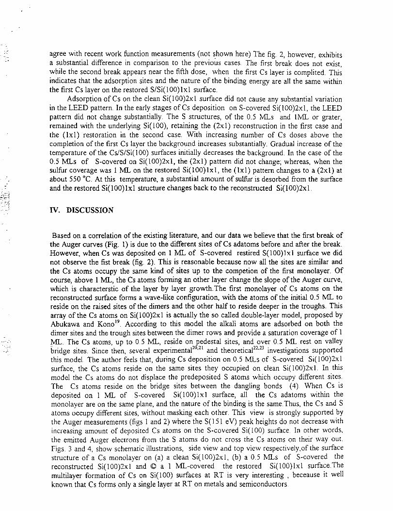
agreewith recentwork functionmeasurements(not shownhere)Thefig. 2, however,exhibitsa substantialdifferencein comparisonto the previouscases.The first breakdoesnot exist,while thesecondbreakappearsnearthefifth dose, when the first Cs layeris complited.Thisindicatesthat theadsorptionsitesandthe natureof the bindingenergyareall the samewithinthefirst Cslayeron therestoredS/Si(100)lxl surface.
Adsorptionof Cs on thecleanSi(100)2xl surfacedid not causeanysubstantialvariationin theLEED pattern.In theearlystagesof Csdeposition on S-coveredSi(100)2xl, theLEEDpatterndid not changesubstantially.The S structures,of the 0.5 MLs and 1ML or grater,remainedwith the underlyingSi(100),retainingthe (2xl) reconstructionin the first caseandthe (lxl) restoration in the secondcase.With increasingnumberof Cs dosesabovethecompletionof thefirst Cs layer the background increases substantially. Gradual increase of the
temperature of the Cs/S/Si(100) surfaces initially decreases the background. In the case of the
0.5 MLs of S-covered on Si(100)2xl, the (2xl) pattern did not change; whereas, when the
sulfur coverage was 1 ML on the restored Si(100)lxl, the (lxl) pattern changes to a (2xl) at
about 550 °C. At this temperature, a substantial amount of sulfur is desorbed from the surface
and the restored Si(100) lxl structure changes back to the reconstructed Si(100)2xl.
IV. DISCUSSION
Based on a correlation of the existing literature, and our data we believe that the first break of
the Auger curves (Fig. 1) is due to the different sites ofCs adatoms before and after the break.
However, when Cs was deposited on I ML of S-covered restired S(100)Ixl surface we did
not observe the fist break (fig. 2). This is reasonable because now all the sites are similar and
the Cs atoms occupy the same kind of sites up to the competion of the first monolayer. Of
course, above 1 ML, the Cs atoms forming an other layer change the slope of the Auger curve,
which is characterstic of the layer by layer growth.The first monolayer of Cs atoms on the
reconstructed surface forms a wave-like configuration, with the atoms of the initial 0.5 ML to
reside on the raised sites of the dimers and the other half to reside deeper in the troughs. This
array of the Cs atoms on Si(100)2xl is actually the so called double-layer model, proposed by
Abukawa and Kono _9. According to this model the alkali atoms are adsorbed on both the
dimer sites and the trough sites between the dimer rows and provide a saturation coverage of 1
ML. The Cs atoms, up to 0.5 ML, reside on pedestal sites, and over 0.5 ML rest on valley
Bridge sites. Since then, several experimental 2°'2_ and theoretical 2z23 investigations supported
this model. The author feels that, during Cs deposition on 0.5 MLs of S-covered Si(100)2xl
surface, the Cs atoms reside on the same sites they occupied on clean Si(100)2xl. In this
model the Cs atoms do not displace the predeposited S atoms which occupy different sites.
The Cs atoms reside on the bridge sites between the dangling bonds (4). When Cs is
deposited on 1 ML of S-covered Si(100)lxl surface, all the Cs adatoms within the
monolayer are on the same plane, and the nature of the binding is the same.Thus, the Cs and S
atoms occupy different sites, without masking each other. This view is strongly supported by
the Auger measurements (figs 1 and 2) where the S(151 eV) peak heights do not decrease with
increasing amount of deposited Cs atoms on the S-covered Si(100) surface. In other words,
the emitted Auger electrons from the S atoms do not cross the Cs atoms on their way out.
Figs. 3 and 4, show schematic illustrations, side view and top view respectively, of the surface
structure of a Cs monolayer on (a) a clean Si(100)2xl, (b) a 0.5 MLs of S-covered the
reconstructed Si(100)2xl and © a 1 ML-covered the restored Si(100)lxl surfaceThe
multilayer formation of Cs on Si(100) surfaces at RT is very interesting , beceause it well
known that Cs forms only a single layer at RT on metals and semiconductors.

* Correspondingauthor
AcknowledgementsWe wishto acknowledgethepartialsupportby NASA GrantNo. NCC3-286 andtheNASAHiPPACCenterat Clark AtlentaUniversityGrantNo. NAG3-1394.
.i; L"
REFERENCES
1. C. A. Papageorgopoulos, Surf. Sci., 104 (1981), 643.
2. G.N. Hatsopoulos and E. P. Gyftopoulos, Thermionic Conversion, MIT Press,
Cambridge, Mass., (1979).
3. D. Edwards and W. T. Perria, Appl. Surf. Sci., 1 (1979), 419.
4. Ads Papageorgopoulos and M. Kamaratos, Surf. Sci., (1996), in print.
5. R.D. Bringans, R. I. G. Uhrberg and R. Z. Bechrach, Phys. Rev. B 34 (1986), 2373.
6. R.R.G. Uhrberg, R. D. Brigans, M. A. Olmstead, R. Z. Brachrach and J. E.
Northup, Phys. Rev. B 35 (1987), 3945.
7. M Copel, M. C. Reuter, E. Kaxiras and R. M. Tromp, Phys. Rev. Lett., 63 (1989),632.
8. M.H. Tsai and R. V. Kasowski, Phys. Rev. Lett., 60 (1988), 546.
9. H. Ishida and K. Terakura, Phys. Rev. B, 40 (1989), 11519.
10 Y. Ling, A. J. Freeman and B. Delley, Phys. Rev. B, 39 (1989), 10144.
11 Y. Ma, P. Rudolf, C. T. Chen and F. Sette, J. Vac. Sci. Technol. A, 10 (1992),1965.
12. J.D. Levine, Surf. Sci., 34 (1973), 90.
13. H. Tochihara and Y. Murata, J. Phys. Soc., Japan, 51 (1982), 2920.
14. H. Tochihara, Surf. Sci., 126 (1983), 523.
15. T. Aruga, H. Tochihara and Y. Murata, Phys. Rev. Lett., 53 (1984), 372.16. H. Tochihara and Y. Murata, Surf. Sci., 215 (1989), L323.
17. C. M. Wei, H. Huang, S. Y. Tong, G. S. Glander and M. B. Webb, Phys. Rev. B 42
(1990), 1124.
.18. L. Spiess, P. S. Mangat, S. P. Tang, K. M. Schirm, A. J. Freeman and P.Souldassian,
Surf. Sci. Lett., 289 (1993), L 637.
19. T. Abukawa and S. Kono, Phys. Rev. B 37 (1988), 9097.221 (1989), 263.
20. A. J. Smith, W. R. Graham and E. W. Plummer, Surf. Sci. Lett.,243 (1991), 437.
21. J. Urano, S. Hongo and T. Kanji, Surf. Sci.,(1993) 287/288, 249
22; B.L. Zhang, C. T. Chan and K. M. Ho, Phys. Rev.B 44 (1991), 8210.
23. Y. Marikawa, K. Kobayashi and K. Terakura, Surf. Sci. 283 (1993) 377.
Figure Caption
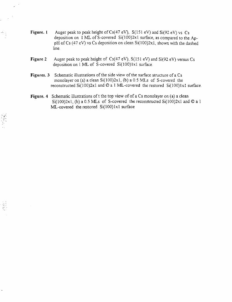
Figure. 1
Figure 2
Figures. 3
Figure. 4
Auger peak to peak height ofCs(47 eV), S(151 eV) and Si(92 eV) vs Cs
deposition on 1 ML of S-covered Si(100)2xl surface, as compared to the Ap-
pH of Cs (47 eV) vs Cs deposition on clean Si(100)2xl, shown with the dashedline.
Auger peak to peak height of Cs(47 eV), S(151 eV) and Si(92 eV) versus Cs
deposition on 1 ML of S-covered Si(100)lxl surface.
Schematic illustrations of the side view of the surface structure of a Cs
monolayer on (a) a clean Si(100)2xl, (b) a 0.5 MLs of S-covered the
reconstructed Si(100)2xl and © a 1 ML-covered the restored Si(100)lxl surface.
Schematic illustrations of t the top view of of a Cs monolayer on (a) a clean
Si(100)2xl, (b) a 0.5 MLs of S-covered the reconstructed Si(100)2xl and © a 1
ML-covered the restored Si(100)lxl surface

0
Ap-pH (arb. units)
c_A 0 _'_0 0 0 0
x
X
X
X
x
X
X
x
X
x
X
VA
b00
[ I
..q _z_ ba(_ _
x
L_

(sl!un "q.t_) H d-d V

a-
(a)
,_,a'_! s_,Ss',,
(b)
(c)

,: .i
Cs
Si
(b)
© ©
tel