final presentation
DESCRIPTION
mehr und mo0retzTRANSCRIPT
1Electronic Products and Systems Center
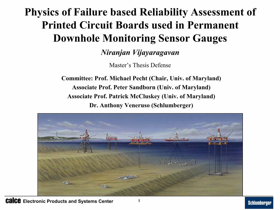
Physics of Failure based Reliability Assessment of Printed Circuit Boards used in Permanent
Downhole Monitoring Sensor GaugesNiranjan Vijayaragavan
Committee: Prof. Michael Pecht (Chair, Univ. of Maryland)Associate Prof. Peter Sandborn (Univ. of Maryland)
Associate Prof. Patrick McCluskey (Univ. of Maryland)Dr. Anthony Veneruso (Schlumberger)
Master’s Thesis Defense

2Electronic Products and Systems Center
Objective• To perform a reliability assessment of interconnects and
components in printed circuit boards used in sensor gauges for permanent monitoring of oil wells
• Specifically – Identify life cycle loads associated with electronics used for oil and
gas exploration and production applications and propose a methodology to develop life cycle profiles to assess life cycle loads at each phase
– Identify interconnect and component level failure mechanisms associated with printed circuit boards used in permanent downhole monitoring applications
– Perform accelerated thermal testing to assess reliability of the gauge electronics at its operating temperature conditions for an extended period of time

3Electronic Products and Systems Center
Presentation Outline
• Permanent monitoring systems• Hyper permanent quartz gauge (HPQG*)• Physics of failure based reliability assessment of the HPQG
– Virtual reliability assessment• Design capture• Life cycle profile • Failure modes, effects and criticality analysis (FMECA)• IC level design capture• Board level stress and damage analysis• Component level stress and damage analysis
– Accelerated thermal testing
• Reliability analysis results and conclusions • Contributions
* - HPQG is a trademark of Schlumberger

4Electronic Products and Systems Center
Permanent Downhole Monitoring Systems• Permanent monitoring systems are used in modern day oil extraction and
production for real time monitoring of oil reservoir conditions e.g., temperature and pressure
• Real time monitoring of oil reservoir conditions provides for better reservoir management and production optimization1-10
• Life of 5 to 10 years is required (high intervention cost)• It has been shown that a substantial percentage of failures in downhole
monitoring systems is caused by failures in the electronic gauges1,8,9
Downholegauges
Data acquisitionunit
MonitoringcomputerData link

5Electronic Products and Systems Center
Hyper Permanent Quartz Gauge (HPQG)
• Hyper Permanent Quartz Gauge (HPQG) - sensor gauge used by Schlumberger for permanent monitoring applications
• Consists of two printed circuit boards (PQG101 & PQG202) and three quartz crystals (pressure, temperature and reference)
– Quartz crystals have proven long term reliability under harsh environmental conditions27,34
• Temperature crystal – change frequency of vibration in response to temperature
• Pressure crystal – change frequency of vibration in response to pressure
• Reference crystal – produce a frequency to mix the pressure and temperature crystalsignals appropriately and scale to lower frequency ranges
– PQG101 printed circuit board consists of digital, power and telemetry circuitry
– PQG202 printed circuit board consists of oscillators and frequency mixers to interface with the quartz crystals

6Electronic Products and Systems Center
HPQG Construction and Assembly
Digitizer, Power and telemetry board (PQG101)
Quartz sensors (temperature, pressure and reference crystals)
Oscillator and mixer board (PQG202)
To oil reservoirs
Generate frequency signals corresponding
to the pressure and temperature conditions
Mix the frequency signals from the crystals with the
reference frequency
Digitize the frequency signals and send it to
the data acquisition unit
Operational assembly
Mechanical assembly
Steel tubing
Insulating sheet (damping element)
PCB
Steel chassis Hermetically sealed assembly

7Electronic Products and Systems Center
Reliability Assessment of the HPQG• Past efforts - statistical data and similarity analysis methods from similar systems in the field1-8
• Majority of the HPQG installations have operated below 100oC6
• Installations above 125oC - few and inadequate to predict the reliability of the gauges • Therefore to assess reliability of the HPQG for operation up to 150oC, physics of failure based
reliability methodology developed by CALCE, University of Maryland was used• Results can be used as guidelines for development of equipment for higher temperatures
Board level assessment Component level assessment Accelerated testing
Identification of potential reliability issues
FMECA Updated FMECA
8Electronic Products and Systems Center
Physics of Failure based Reliability Assessment of the HPQG

9Electronic Products and Systems Center
Design Capture
• All parts were insertion mounted• All ICs were dual inline packages• Connectors were modeled as single inline packages, axial diodes, inductors and
resistors as axial packages, canned transistors and box capacitors/resistors as pin grid array packages
• All parts were soldered with High Melting Point (HMP - 93.5%Pb, 5% Sn, 1.5% Ag; Solidus 296°C)
Interconnect informationSolder area and height
Lead geometry and dimensionsSolder materialLead material
Board informationBoard layers and composition
Board dimension (x,y,z)Number of drill holes (vias)
Via and capture pad geometryMaterials – Board, solder, trace, via, pad
Part informationDimensions
Location on PCBPackage standoff
Junction to case thermal resistance (θJC)
Power dissipationPackage material
The boards PQG101 and PQG202 were modeled using calcePWA23-25 software

10Electronic Products and Systems Center
Design Capture (Continued)
• PQG202– 6-layer polyimide single sided board– 79 parts ( 27 unique) – 61 passive and 18 active – 392 drill holes – 137 vias, 250 component lead holes (5 types), 5 clamping holes– Power dissipation – 0.6 W, Dimensions – 7.93 × 0.92 × 0.06 inches
• PQG101– 8-layer polyimide single sided board– 61 parts (40 unique) – 49 passive and 12 active– 490 drill holes – 116 vias, 374 component lead holes (4 types), 6 clamping holes– Power dissipation – 3.1 W, Dimensions – 14.64 × 0.92 × 0.06 inches

11Electronic Products and Systems Center
Design Capture – Detailed Example
Via-D0.7 - D1.4 (PQG101)Drill size – 700 µm (diameter)
Pad size – 1400 µm (diameter)
Plating material – Cu
Finish material – Au
Pad thickness – 35 µm
Plating thickness – 10-12 µm
Finish thickness – 2 µm
via
C8 – E082311 Capacitor (PQG202)100 pF, 50 V Ceramic Capacitor
Power dissipation – 0.36 mW
Package dimensions – 7.6 × 2.4 × 6.1 mm
Package standoff height – 0.42 mm
IO span (distance between pins) – 6 mm
Lead thickness – 0.58 mm
Modeled as a Pin Grid Array package with two leads
Drawings not to scale

12Electronic Products and Systems Center
Life Cycle Profile Development
• A methodology to address life cycle considerations in electronics used for oil and gas extraction and production was developed35
• Steps for developing a life cycle profile:
– Describe expected events for an item or equipment, from manufacture through end of life
– Identify significant natural and induced environmental factors or combinations of environmental factors for each expected phase
– Describe environmental load conditions (in both narrative, absolute and/ or statistical form) to which equipment will be subjected during the life cycle
• Principal effects and associated failures in electronic equipment due to key environmental factors like temperature, relative humidity, pressure, wind, salt spray, sand and dust, air pollution, rain and freezing rain were identified and described
• Importance of considering effects of combined environmental loads was stressed, effects of some combined environmental loads were listed
• The methodology was used to develop the life cycle profile for the HPQG

13Electronic Products and Systems Center
Life Cycle Profile for HPQG• Phases in the life cycle of PQG101 and PQG202
– Manufacturing testing/Screening– Storage at test facility– Transportation to destination– Storage at destination– Transportation to installation site– Installation– Operation
• Significant environmental loads in each stage*
– Temperature– Vibration– Shock
* Factors like moisture and dust are ignored since the boards are in a hermetically sealed assembly

14Electronic Products and Systems Center
00.0050.01
0.0150.02
0.0250.03
0.035
0 100 200 300 400
Frequency (Hz)
PSD
(g^2
/Hz)
0
50
100
150
200
0.00 0.50 1.00 1.50 2.00 2.50 3.00
Time (days)
Tem
pera
ture
(C)
Life Cycle Profile For HPQG• Screening (temperature, vibration)
VibrationTemperature
• Storage at test facility (temperature)– The printed circuit boards are stored at a controlled temperature of approximately 25°C.
For the analysis, the duration is taken as a month• Transportation to destination (temperature, vibration, shock)
– Dependent on ambient temperatures of the source and the destination– Duration is taken as 40 days– Two temperature profiles were developed
• From 43°C to -70°C (corresponds to a low temperature destination and high temperature source)• From -23°C to 58°C (corresponds to a high temperature destination and low temperature source)

15Electronic Products and Systems Center
-60-40-20
020406080
0 10 20 30 40
Time (days)
Tem
pera
ture
(C)
-80-60-40-20
0204060
0 10 20 30 40
Time (days)
Tem
pera
ture
(C)
Life Cycle Profile For HPQG (Continued)
0
100
200
300
400
500
600
0 0.5 1 1.5 2
Time (ms)
Acc
eler
atio
n (g
)
For this presentation all the data shown henceforth will correspond to the low temperature destination analysis. No significant difference was observed in the results between the two different profiles
Transportation vibration profile Transportation
shock profile
Transportation to low temperature
destination profileTransportation to high temperature destination profile
0
0.2
0.4
0.6
0.8
0 500 1000 1500 2000 2500
Frequency (Hz)
PSD
(g^2
/Hz)

16Electronic Products and Systems Center
Life Cycle Profile For HPQG (Continued)• Storage at destination (temperature)
– Normal indoor fluctuations for the duration of one month
• Transportation to installation site (temperature, vibration, shock)– Temperature profile depending on the destination. Duration 6 hours.
• Installation (temperature, vibration, shock)– Duration 30 hours– Temperature profile has a sudden rise when the tool comes into contact with the hot liquid
inside the tubing and a gradual rise as it is lowered down the tubing• Operation (temperature, vibration)
– Constant temperature of 150ºC, Vibration - 3/4th of the duration– One day of dormancy at 25ºC every 6 months
0
0.05
0.1
0.15
0.2
0 100 200 300 400 500
Frequency (Hz)
PSD
(g2 /H
z)
Operation vibration profile
Operation temperature profile
0
50
100
150
200
0 50 100 150 200
Time (days)
Tem
pera
ture
(C)

17Electronic Products and Systems Center
Failure Modes, Effects and Criticality Analysis• FMECA was performed by Schlumberger based on past experience and design details• The FMECA for the HPQG was performed according to the following steps:
– Definition of the system (which components are within the boundaries of the study)– Definition of the main functions of the system– Description of the operational modes of the system and the operational and environmental stresses
that may affect the system– System breakdown into subsystems that can be handled effectively– Preparation of a complete component list for each subsystem– Identification of failure modes and their effects recorded on FMECA worksheets– Determination of criticality for each failure
• The failures were classified in the following ways
Unlikely during five years of operation
Low
Possible during five years of operation
Moderate
Likely during five years of operation
High
Failures that allows operation to continue and data to flow.
Nuisance
Failure that results in some lost data and requires a change in operating conditions or procedures to continue.
Major
Mission critical failure causing permanent loss of electrical connection to downhole equipment.
Critical
Based on occurrence probability Based on criticality
Occurrence probability × criticality = risk in using the part

18Electronic Products and Systems Center
FMECA Key Findings• 38 failure modes were identified and classified as following
1581Low
104Moderate
High
CriticalMajorNuisanceProbability\Criticality
• The 10 critical failures with moderate probability of occurrence identified four IC devices, two capacitors and a resistors
• The identified IC devices were– VQ3001– 80C154– M27C256– DCM92
• OP221 – critical with low probability of occurrence• Failure modes in the ICs were associated to the circuitry, wirebond or the solder joint
19Electronic Products and Systems Center
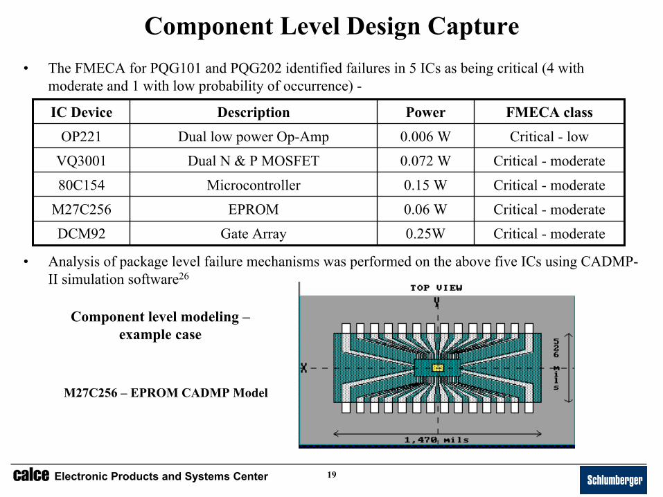
Component Level Design Capture• The FMECA for PQG101 and PQG202 identified failures in 5 ICs as being critical (4 with
moderate and 1 with low probability of occurrence) -
FMECA classPowerDescriptionIC Device
0.25W
0.06 W
0.15 W
0.072 W
0.006 W
Gate Array
EPROM
Microcontroller
Dual N & P MOSFET
Dual low power Op-Amp
Critical - moderateDCM92
Critical - moderateM27C256
Critical - moderate80C154
Critical - moderateVQ3001
Critical - lowOP221
• Analysis of package level failure mechanisms was performed on the above five ICs using CADMP-II simulation software26
M27C256 – EPROM CADMP Model
Component level modeling –example case

20Electronic Products and Systems Center
Component Level Modeling Details M27C256 256Kbit EPROM
Die level detailsDie size – 2.06 x 1.39 mm (0.28 mm thickness)Semiconductor material - siliconGate oxide thickness – 150 Å (Area – 1e-6 m2)Metal thickness – 5000 ÅMetal width – 2 µmMetallization – Al – 1%Si – 0.5%CuPassivation – 5000 Å USG/8000 Å PSG/7000 Å SiON
Dimensions of the metallization was also given
Package level detailsDual Inline Ceramic Package – 3.73 × 1.34 × 0.45 cmCase material – 90% AluminaLid material – 90% AluminaDie Attach Metallization – Bare baseDie Attach material – Silver GlassDie Attach Temperature – 435oC (8-12 min)Bond Finger metallization – AluminumBonding Wire – 31.75 µm diaBonding method – Ultrasonic WedgeSeal material – Vitreous glassSeal temperature – 440oC (10-13min) – Dry AirLead frame material – Alloy 42 AluminatedLead finish – Tin platingCavity moisture - <5000 ppm
Dimensions and geometry of the lead, attach and seal layers werealso given
Calculated values Assumed Defaults
Barrier potential – 0.7VAvalanche breakdown voltage – 50VDrain to source voltage – 5V
Power dissipation – 0.018 WWorst case current density – 2e+7 A/m2
Current – 30 mA
Manufacturer Data

21Electronic Products and Systems Center
Board Level Thermal Analysis• Thermal analysis was performed at an ambient temperature of 150ºC at full
powered condition - to be used as inputs in the failure models
Steel
SteelInsulatorClamps
PCB
• Boundary conditions– Gauge assembly is at isothermal 150°C– Combined conduction and natural convection analysis was performed using the
finite difference method in calcePWA
Small standoff to protect soldered leadsHot oil surrounding
the tube (isothermal 150ºC)

22Electronic Products and Systems Center
Board Level Thermal AnalysisMaximum increase of 1.6oC was found in PQG101 and an increase of 0.7oC was found in PQG202
150.001 – 150.138
150.138 – 150.271
150.271 – 150.406
150.406 – 150.541
150.541 – 150.676
150.676 – 150.811
150.811 – 150.946
150.946 – 151.081
151.081 – 151.216
151.216 – 151.351
151.351 – 151.486
151.486 – 151.620
PQG101- Thermal profile at 150oC
PQG202 – Thermal profile at 150oC
Note – The temperature profile shows the temperature distribution on the board surface

23Electronic Products and Systems Center
Board Level Vibration Analysis• Finite element vibration analysis was performed for the PSD profiles
described in the life cycle profile – Screening, transportation, installation and operation
Fixed clamps
Standoff - x
Ideal mechanical model
Worst case model
First three fundamental frequency modes are obtained.
The dynamic displacement behavior of the boards is then found by superimposing these results for appropriate frequencies and PSD values from the profile.
Can restrain free deflection

24Electronic Products and Systems Center
• Displacements for operational and transportation vibration conditions are significantly higher than those in qualification and installation
Board Level Vibration Analysis
0.041 –
0.13 0.13 – 0.219
0.219 – 0.308
0.308– 0.397
0.397– 0.486
0.486– 0.575
0.575– 0.664
0.664– 0.753
0.753– 0.842
0.842– 0.931
0.931– 1.020
1.020– 1.109 Minimum Maximum
Displacement Color Map
• PQG202 Vibration stress analysis results – Frequency modes – 575.5Hz, 728.8Hz and 1556.2Hz
Board Level Shock AnalysisPQG202
0.041 –
0.13 0.13 – 0.219
0.219 – 0.308
0.308– 0.397
0.397– 0.486
0.486– 0.575
0.575– 0.664
0.664– 0.753
0.753– 0.842
0.842– 0.931
0.931– 1.020
1.020– 1.109 Minimum Maximum
Displacement Color Map
Displacement of components based on board flexure

25Electronic Products and Systems Center
Board Level Damage and Life Analysis• Board level damage and life analysis were performed using calcePWA
• Solder joint fatigue models* for through-hole components were used to evaluate the board level reliability
– Thermal fatigue for through hole components
– Random vibration fatigue
• Shock was evaluated as an overstress mechanism– Components with interconnects susceptible to shock level failures were identified
• After evaluating the damage due to wear out mechanisms, the failures were ranked in the expected order of the occurrence
* Material constants for HMP were used in the models. However, the model coefficients were used from existing data on Pb-Sn eutectic solder
0.63
0.60
0.15
% remaining life
~100
~100
~100
%Vibration
~0
~0
~0
%Thermal
C5
C4
CR2
Component
PQG101
~1.00
~1.00
0.99
% remaining life
-
-
~100
%Vibration
-
-
~0
%Thermal
R29
TP7
C18
Component
PQG202
26Electronic Products and Systems Center
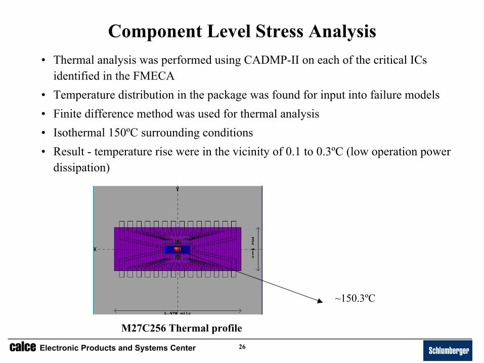
Component Level Stress Analysis• Thermal analysis was performed using CADMP-II on each of the critical ICs
identified in the FMECA• Temperature distribution in the package was found for input into failure models• Finite difference method was used for thermal analysis• Isothermal 150ºC surrounding conditions• Result - temperature rise were in the vicinity of 0.1 to 0.3ºC (low operation power
dissipation)
M27C256 Thermal profile
~150.3ºC

27Electronic Products and Systems Center
Component Level - Damage and Life Analysis• Component level damage and life analysis were done using CADMP26
• On-chip and package level failure models were used
• The failure mechanisms evaluated:– Electromigration17
– Hermetic metallization corrosion21
– Time dependent dielectric breakdown (Fowler Nordheim Tunneling model)20
– Wire fatigue18,22
– Bond pad fatigue22
– Wire bond pad shear fatigue22
• Models for each failure mechanism were checked and modified for appropriate constants and formulae against the original models from the literature
• Temperature values from the stress analysis were used as input to various reliability analysis failure models

28Electronic Products and Systems Center
Component Level Damage and Life Analysis - Results• No failures were predicted during the 5 year operating life of the ICs• Predominant degradation mechanisms – electromigration and metallization corrosion
0.988Metallization corrosion
0.979Electromigration
% remaining lifeFailure model
0.997Metallization corrosion
0.995Electromigration
% remaining lifeFailure model
0.994Metallization corrosion
0.970Electromigration
% remaining lifeFailure model
0.995Metallization corrosion
0.949Electromigration
% remaining lifeFailure model
OP221
80C154
M27C256
DCM 92
0.995Metallization corrosion
0.994Electromigration
% remaining lifeFailure modelVQ3001

29Electronic Products and Systems Center
Component Level Damage – Sensitivity Analysis
% Remaining life of DCM92 at different temperatures175ºC150ºC125ºC
0.9950.9950.995Metallization corrosion
0.8720.9490.983Electromigration
Electromigration accelerates faster than metallization corrosion due to temperature
30Electronic Products and Systems Center
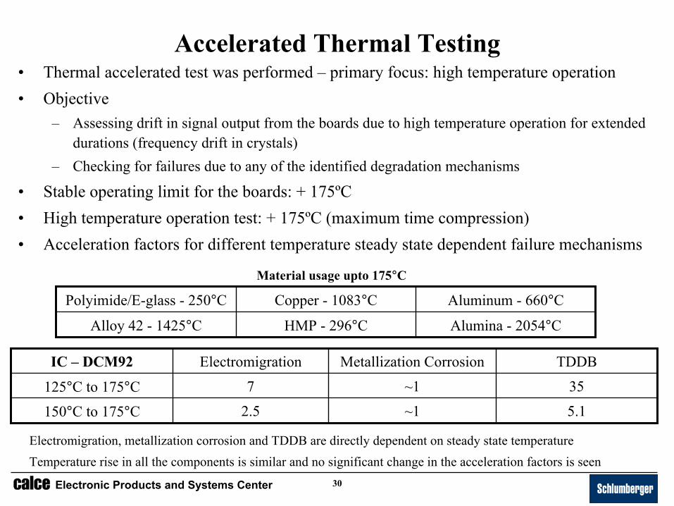
Accelerated Thermal Testing• Thermal accelerated test was performed – primary focus: high temperature operation• Objective
– Assessing drift in signal output from the boards due to high temperature operation for extended durations (frequency drift in crystals)
– Checking for failures due to any of the identified degradation mechanisms
• Stable operating limit for the boards: + 175ºC• High temperature operation test: + 175ºC (maximum time compression)• Acceleration factors for different temperature steady state dependent failure mechanisms
Electromigration, metallization corrosion and TDDB are directly dependent on steady state temperatureTemperature rise in all the components is similar and no significant change in the acceleration factors is seen
5.1~12.5150°C to 175°C
35~17125°C to 175°C
TDDBMetallization CorrosionElectromigrationIC – DCM92
Alumina - 2054°CHMP - 296°CAlloy 42 - 1425°C
Aluminum - 660°CCopper - 1083°CPolyimide/E-glass - 250°C
Material usage upto 175°C

31Electronic Products and Systems Center
Accelerated Test Setup• Two HPQG assemblies were prepared and placed in the thermal chamber• The hardware required for the accelerated test setup was –
Solder equipmentOscilloscopePC and a data collection softwareA gauge simulatorA thermal chamber capable of going upto 175oC
Two printed circuit boards PQG101Two printed circuit boards PQG2024 Temperature crystals* and 2 reference crystalsData acquisition unit High temperature wires
• HPQG preparation– Boards were baked at 125oC for one day– PQG202 was soldered with two temperature crystals* and one reference crystal– PQG202 was then connected to PQG101 using six high temperature wires– Soldering was done using HMP
• Output from each PQG101 was connected to the data acquisition unit• The third port of the data acquisition unit was connected to a gauge simulator• Data acquisition unit was connected to a PC loaded with monitoring software
* - As a sub-objective, it was decided to test how compatible temperature crystals are on the pressure line of the PQG electronic boards, considering that the frequency outputs from the pressure and temperature crystal are very close to each other. Hence each PQG202 had two temperature crystal instead of one pressure and one temperature crystal.

32Electronic Products and Systems Center
Accelerated Test Setup (Continued)
Two sets of HPQG assemblies in the thermal chamber
Gauge simulator
Thermal chamber
Monitoring PC, data acquisition unit, gauge
simulator and oscilloscope
Data acquisition unit - interior
Signal from HPQG
Signal from HPQG
Dummy Signal from simulator
Data rea
dout

33Electronic Products and Systems Center
• Purpose - electrical response not calibrated to surrounding conditions• Test
– Step test: 25ºC to 175ºC in steps of 25ºC – Dwell – 12 hours, maximum ramp rate 5ºC/min
• Results– Calibration chart – coefficients input to the monitoring software– Pressure line has a slight non-linear response with temperature– Stable operation up to 175ºC – No hysteresis in the output– Stable output at constant temperature
Calibration
Failure Criteria• One or both output lines of either board stop responding• The frequency response of the crystals drifts away from the range of 10 KHz to 50
KHz permanently or temporarily• This was translated into ±10% drift in the mean value of the outputs from the boards
• There is ± 25% variation (a spike) in any measurement from the mean value

34Electronic Products and Systems Center
Accelerated Testing – Process and Results• Steady state temperature of 175oC• Hourly data was stored• Real time data updated every second was displayed on the PC• Alarms were set at temperatures of 135oC and 215°C to give a warning if the
temperature measurement went beyond these limits• The test was stopped after 4500 hours of high temperature testing
165
167
169
171
173
175
177
179
181
183
185
0 1000 2000 3000 4000
Time (hours)
Tem
pera
ture
line
res
pons
e (C
)
165
167
169
171
173
175
177
179
181
183
185
0 1000 2000 3000 4000
Tim e (hours)
Tem
prea
ture
line
res
pons
e (C
)
HPQG-1 Temperature line response HPQG-2 Temperature line response
There was much more variation in the pressure line compared to the temperature line. Temperature crystal in the pressure line is not suitable as a reliable temperature sensor
35Electronic Products and Systems Center
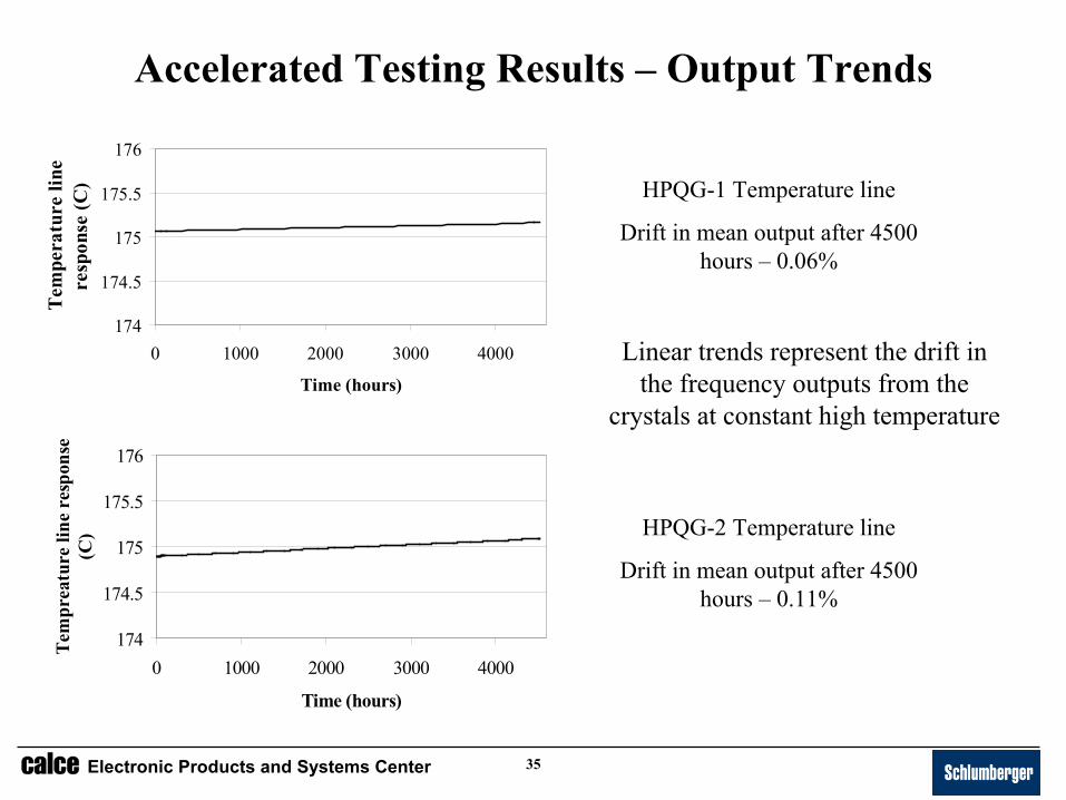
Accelerated Testing Results – Output Trends
HPQG-1 Temperature line
Drift in mean output after 4500 hours – 0.06%
HPQG-2 Temperature line
Drift in mean output after 4500 hours – 0.11%
Linear trends represent the drift in the frequency outputs from the
crystals at constant high temperature
174
174.5
175
175.5
176
0 1000 2000 3000 4000
Time (hours)
Tem
pera
ture
line
re
spon
se (C
)
174
174.5
175
175.5
176
0 1000 2000 3000 4000
Time (hours)
Tem
prea
ture
line
res
pons
e (C
)

36Electronic Products and Systems Center
Accelerated Testing – Observations and Conclusions• No failures
– Measurements remained within +/- 25% of measured value (175oC)
– Both HPQGs were fully functional
– Negligible drift in response (0.06% in HPQG-1, 0.11% in HPQG-2)
• Visual Inspection– No opens or shorts were found
– Benign cracks were found on few of the capture pads and traces
• 4500 hours @ 175oC – boards were fully functional– 0.11% maximum drift
– Thus, in 5 years the maximum drift expected – 1.07%
• Thus, boards are not expected to fail in 5 years of operation at 150°C due to high temperature operation.

37Electronic Products and Systems Center
Reliability Analysis Summary and Conclusions• Life cycle environmental profile for the printed circuit boards was developed
• Electromigration and hermetic metallization corrosion are expected to be the leading degradation mechanisms at the component level*
• Solder joint fatigue due to vibration is expected to be the leading wear out mechanism at the board interconnection level
• No failures are expected due to degradation mechanisms
• Interconnects with higher risk of shock failure were identified
• Acceleration factors for different steady-state temperature dependent failure mechanisms were calculated
• Temperature accelerated test was performed – no failures expected in 5 years of operation at 150ºC
• Boards are reliable for operation at 150ºC for 5 years
* It was confirmed by Schlumberger that electromigration and metallization corrosion were their prime concerns for reliability, with electromigration being the most critical

38Electronic Products and Systems Center
IEEE 1413 Analysis of the Prediction Methodology36,37
• Does the methodology identify the source used to develop the prediction methodology and describe the extent
to which the source is known? - Yes
• Are assumptions used to conduct the prediction according to the methodology identified, including those used
for any unknown data? - Yes
• Are limitations of the prediction results identified? - Yes
• Are sources of uncertainty in the prediction results identified? - Yes
• Are failure modes identified? - Yes
• Are failure mechanisms identified? - Yes
• Are confidence levels for the prediction results identified? - No
• Does the methodology account for life cycle environmental conditions, including those encountered during a)
product usage (including power and voltage conditions), b) packaging, c) handling, d) storage e) transportation,
and f) maintenance conditions? - Yes
• Does the methodology account for materials, geometry, and architectures that comprise the parts? - Yes
• Does the methodology account for part quality? - Yes
• Does the methodology allow incorporation of reliability data and experience? - Yes

39Electronic Products and Systems Center
Contributions• Developed a methodology to assess environmental
considerations in electronic equipment used for oil and gas extraction applications and listed effects of associated individual and combined environmental factors on electronic equipment
• Identified failure mechanisms of concern associated with permanent downhole monitoring electronic gauges
– Vibration and shock at board level
– Electromigration and metallization corrosion at IC level

40Electronic Products and Systems Center
Future Work and Recommendations
• Instrument downhole equipment to find actual environmental conditions
• Perform combined vibration and temperature accelerated testing
• Evaluate shock level reliability
• Improve assembly technology to reduce shock and vibration effects
– Migrate to surface mount technology – reduce board area
– Use better packing technologies – damping layers in contact with the board
– Use better clamping mechanisms e.g., clamping along the sides
• Research advanced materials for future extended temperature applications (~175oC +)

41Electronic Products and Systems Center
Publications• Book chapter
– Vijayaragavan, N., Donahue, D., Pecht, M., “Life cycle determination”, chapter in ‘Part Selection and Management’ published by John Wiley and Sons
• Papers to be submitted– Vijayaragavan, N., Das, D., Pecht, M., Veneruso, A., “Physics of failure
based reliability assessment of printed circuit boards used for permanent monitoring applications”
– Vijayaragavan, N., Das, D., Pecht, M., Veneruso, A., “Uprating of military grade components for downhole reservoir monitoring applications”
– Vijayaragavan, N., Das, D., Pecht, M., Veneruso, A., “A standard for assessing environmental considerations in electronics used in oil and gas exploration and production applications”

42Electronic Products and Systems Center
References1. Gisbergen, S.J.C.H.M., Vandeweijer, A.A.H., “Reliability analysis of permanent downhole
monitoring systems”, Offshore Technology Conference, OTC 10945, May, 1999.2. Baker, A., Jeffery, J., Thomas, A., Unneland, T., “Permanent monitoring – looking at lifetime
reservoir dynamics”, Oilfield Review 7, No. 4, 1995, pp. 32-46.3. Eck, J. et al, “Downhole monitoring : The story so far”, Oilfield Review 7, No. 4, 1999/2000, pp. 20-
33.4. Unneland, T., Manin, Y., Kuchuk, F., “Permanent gauge pressure and rate measurements of reservoir
description and well monitoring: field cases”, SPE Annual Technical Conference and Exhibition, SPE 38638, San Antonio, TX, October, 1997.
5. Athichanagom, S., Horne, R., Kikani, J., “Processing and interpretation of long-term data from permanent downhole pressure gauges”, SPE Annual Technical Conference and Exhibition, SPE 56419, Houston, TX, October 1999.
6. Veneruso, A.F., Hiron, S., Bhavsar, R., Bernard, L., “Reliability qualification testing for permanently installed wellbore equipment”, SPE Technical Conference and Exhibition, SPE 62955, Dallas, TX, October 2000.
7. Brownlee, F., Eriksen, R., Goldsmith, R., Wylie, G., “Improving well completion system reliability using intelligent well technology”, Offshore Technology Conference, OTC 13029, Houston, TX, 2001.
8. Drakeley, B., Douglas, N., Haugen, K., Willmann, E., “Application of reliability analysis techniques to intelligent wells”, Offshore technology conference, OTC 13028, Houston, TX, 2001.
9. Boer, J.J., “The use of high temperature electronics in downhole applications”, Proceedings of the HITEN Conference, Berlin, July 1999.

43Electronic Products and Systems Center
References10. Gingerich, B.L., Brusius, P.G., Maclean, I.M., “Reliable electronics for high-temperature downhole
applications”, SPE Annual Technical Conference and Exhibition, Houston, TX, October 1999. 11. Veneruso, A.F., Kosmala, A.G., Bhavsar, R., Bernard, L.J., Pecht, M., “Engineered reliability for
intelligent well systems,” Offshore Technology Conference, OTC 13031, Houston, Texas, 30 April–3 May, 2001.
12. Pecht, M., Radojcic, R., Rao, G., ‘Guidebook for managing silicon chip reliability’, CRC Press, Boca Raton, FL, 1999.
13. Pecht, M., Lall, P., Hakim, E., ‘Influence of temperature on microelectronics and system reliability’, CRC Press, New York, NY, 1997.
14. McCluskey, F.P., Grzybowski, R., Podlesak, T., ‘High temperature electronics’, CRC Press, New York, NY, 1997.
15. Barker, D., Dasgupta, A., Pecht, M., “PWB solder joint life calculations under thermal and vibrational loading”, Journal of the IES, Vol. 35, No.1, February 1992, pp. 17-25.
16. Dasgupta, A., “Failure mechanism models for cyclic fatigue,” IEEE Transactions on Reliability, Vol. 42, No. 4, December 1993, pp. 548-555.
17. Black, J. R.,"Physics of electromigration”, IEEE Proceedings of the International Reliability Physics Symposium, 1983, pp. 142-149.
18. Hu, J. M., Pecht, M., Dasgupta, A., "A probabilistic approach for predicting thermal fatigue life of wirebonding in microelectronics", ASME Journal of Electronics Packaging, Vol. 113, 1991, pp. 275-285.
19. Kidson, G.V., "Some aspects of the growth of diffusion layers in binary systems", Journal of Nuclear Materials 3, No.1, 1961, pp. 21-29.

44Electronic Products and Systems Center
References20. McPherson, J.W., Khamankar, R.B., Shanware, A.,"A complementary molecular-model for
TDDB in SiO2 dielectrics", Microelectronics Reliability 40(8-10) , 2000, pp.1591-1597. 21. Pecht, M., Ko, W., "A corrosion rate equation for microelectronic die metallization", International
Journal for Hybrid Microelectronics, Vol. 13, No. 2, June 1990, pp. 41-52.22. Pecht. M., Dasgupta, A., Lall, P., "A failure prediction model for wire bonds", Proceedings of the
International Microelectronic Symposium, ISHM, 1989, pp. 607-603.23. Rothman, T., Dasgupta, A., Hu, J. M., “Test-time compression for qualification testing of
electronic packages: a case study,” Proceedings of the Annual Reliability and Maintainability Symposium, 1995, pp. 246-252.
24. Cunningham, J., Valentin, R., Hillman, C., Dasgupta, A., Osterman, M., “A demonstration of virtual qualification for the design of electronic hardware,” ESTECH 2001, IEST, Phoenix, AZ, April, 2001.
25. Osterman, M., Stadterman, T., "Failure-assessment software for circuit-card assemblies," Proceedings of the Annual Reliability and Maintainability Symposium, January, 1999, pp. 269-276.
26. Lall, P., Hakim, E., “Physics of failure based computer tools for the design of microelectronic packages”, Proceedings of the 2nd ESA Electronic Components Conference, Noordjwik, The Netherlands, May, 1993.
27. “Three crystal transducer assembly”, Quartzdyne, Inc., retrieved on 31st October, 2002 from http://www.quartzdyne.com/technology/3crystal.htm
45Electronic Products and Systems Center
References28. Young, D., Christou, A., “Failure mechanism models for electromigration”, IEEE Transactions on
Reliability, Vol. 43, No. 2, 1994, pp. 186 – 192.29. Pecht, M., Dasgupta, A., “Physics-of-failure: an approach to reliable product development”,
Proceedings of Institute of Environmental Sciences, August, 1995, pp.111-117.30. Pecht, M., “Physics of failure approach to design and reliability assessment of microelectronic
packages”, Proceedings of the First International Conference on Microelectronic and PCB Technology, Beijing, China, Sept. 1994, pp. 175-180.
31. Pecht, M., Lall, P., “Integrated physics of failure approach to reliability assessment”, Advances in Electronic Packaging ASME EEP, Vol. 4, No. 1, 1993.
32. Pecht, M., Bauernshub, R., Lall, P., “A PoF approach to addressing defect related reliability”, Proceeding of the 6th Electronics Manufacturing Symposium, LaJolla, CA, September 1994, pp. 38-49.
33. Pecht, M., et al, “The transition from statistical- field failure models to physics of failure based models for reliability assessment of electronic packages”, Proceedings of the INTERpack’95, Lahina, Maui, HI, March 1995, pp. 619-625.
34. Matsumoto, N., Sudo, Y., Sinha, B., Niwa, M., “Long term stability and performance characteristics of crystal quartz gauge at high pressure and temperatures”, Joint Meeting EFTF-IEEE IFCS, 1999, pp. 1019-1022.
35. Lewis Research Center, NASA, “NASA preferred reliability practices – environmental factors,” Practice Number PD-EC-1101, retrieved on 2nd June, 2002 from http://www.hq.nasa.gov/office/codeq/relpract/np1101.pdf

46Electronic Products and Systems Center
References36. IEEE Std 1413.1-2002, “IEEE Guide for Selecting and Using Reliability Predictions Based on
IEEE 1413TM”, IEEE Standards Coordinating Committee 37 on Reliability Prediction, IEEE, New York, NY, 19th February, 2003, pp. 41-49, 55-63.
37. IEEE Std 1413-1998, “IEEE Standard Methodology for Reliability Prediction and Assessment of Electronic Systems and Equipment”, Standards and Definitions Committee of the IEEE Reliability Society, IEEE, New York, NY, 15th January 1999.