final cp
TRANSCRIPT

CHAPTOR 1
MICROCONTROLLER BASED CAR PARKING SYSTEM
INTRODUCTION
In the project “Car Parking System” we have shown the concept of an automatic car
parking system. As in the modern world everything is going automatic we have built a
system which will automatically sense the entry and exit of cars through the gate and
then display the number of cars in the parking lot. Even we can set a maximum capacity
of cars so that there is no congestion. We have deployed a microcontroller which is used
to sense the movement of cars and depending upon whether there is a capacity of cars to
enter, it either opens the gate or not.
There are two sets of sensors: one before the gate and one after the gate. When a car
arrives at the door the microcontroller receives the signal from the entry sensors and
then checks whether there is a capacity of cars to be accommodated. If it’s so it will
command the stepper motor to open the door and after some time (say 5 seconds) it will
shut the door. Simultaneously it will also display the number of cars present in the
parking lot on a LCD screen. When a car moves out of the parking area the
microcontroller reduces the count displayed accordingly. The user will have an option to
set the maximum count for the cars with the help of switches connected to the
microcontroller.
The sensing of entry and exit of cars is done with the help of Infrared transmitters and
receivers. Before the door the Infrared transmitter is mounted on one side and the
receiver is placed directly in front of the transmitter across the door. When a car arrives
the Infrared beam is blocked by the car and the receiver is devoid of Infrared rays and its
output changes. This change in output is sensed by the microcontroller and accordingly
it increments the count and opens the door if there is some capacity. The procedure for
the exit of the cars is similar as the entry.

But a problem arises that when a car enters the parking area, firstly the Infrared beam at
the entry (First beam) is blocked and then the beam at the other side (Second beam) of
the door is blocked. But the blocking of the second beam should not be considered as the
exit of car since it is the second beam, which is blocked when the car exits the parking.
So it means that every time a car enters or exits both the beams are blocked. To
eliminate this problem we program the microcontroller to sense the order of blocking of
the two beams. If the first beam is blocked first and then the second beam is blocked, it
means that the car has entered the parking. If the second beam is blocked first and then
the first beam is blocked it means that the car moved out of the parking. Depending
upon this the microcontroller will perform the appropriate action.
BLOCK DIAGRAM

POWER SUPPLY DESCRIPTION
The power supply c:
The transformer steps down the 220 V a/c. into 12 V a/c. The transformer work on the
principle of magnetic induction, where two coils: primary and secondary are wound
around an iron core. The two coils are physically insulated from each other in such a
way that passing an a/c. current through the primary coil creates a changing voltage in
the primary coil and a changing magnetic field in the core. This in turn induces a
varying a/c. voltage in the secondary coil.
The a/c. voltage is then fed to the bridge rectifier. The rectifier circuit is used in most
electronic power supplies is the single-phase bridge rectifier with capacitor filtering,
TRANSFORMER
SHUNT CAPACITOR
BRIDGE RECTIFIER
VOLTAGE REGULATOR

usually followed by a linear voltage regulator. A rectifier circuit is necessary to convert
a signal having zero average value into a non-zero average value. A rectifier transforms
alternating current into direct current by limiting or regulating the direction of flow of
current. The output resulting from a rectifier is a pulsating D.C. voltage. This voltage is
not appropriate for the components that are going to work through it.
1N4007
12-0-12 V
1000uF
TRANSFORMER
The ripple of the D.C. voltage is smoothened using a filter capacitor of 1000 microF
25V. The filter capacitor stores electrical charge. If it is large enough the capacitor will
store charge as the voltage rises and give up the charge as the voltage falls. This has the
effect of smoothing out the waveform and provides steadier voltage output. A filter
capacitor is connected at the rectifier output and the d.c voltage is obtained across the
capacitor. When this capacitor is used in this project, it should be twice the supply
voltage. When the filter is used, the RC charge time of the filter capacitor must be short
and the RC discharge time must be long to eliminate ripple action. In other words the
capacitor must charge up fast, preferably with no discharge.
When the rectifier output voltage is increasing, the capacitor charges to the peak voltage
Vm. Just past the positive peak, the rectifier output voltage starts to fall but at this point
the capacitor has +Vm voltage across it. Since the source voltage becomes slightly less
than Vm, the capacitor will try to send current back through the diode of rectifier. This
reverse biases the diode. The diode disconnects or separates the source the source form
load. The capacitor starts to discharge through load. This prevents the load voltage from
falling to zero. The capacitor continues to discharge until source voltage becomes more
than capacitor voltage. The diode again starts conducting and the capacitor is again
7812
7805

charged to peak value Vm. When capacitor is charging the rectifier supplies the charging
through capacitor branch as well as load current, the capacitor sends currents through the
load. The rate at which capacitor discharge depends upon time constant RC. The longer
the time constant, the steadier is the output voltage. An increase in load current i.e.
decrease in resistance makes time constant of discharge path smaller. The ripple increase
and d.c output voltage V dc decreases. Maximum capacity cannot exceed a certain limit
because the larger the capacitance the greater is the current required to charge the
capacitor.
The voltage regulator regulates the supply if the supply if the line voltage increases or
decreases. The series 78xx regulators provide fixed regulated voltages from 5 to 24
volts. An unregulated input voltage is applied at the IC Input pin i.e. pin 1 which is
filtered by capacitor. The out terminal of the IC i.e. pin 3 provides a regular output. The
third terminal is connected to ground. While the input voltage may vary over some
permissible voltage range, and the output voltage remains constant within specified
voltage variation limit. The 78xx IC’s are positive voltage regulators whereas 79xx IC’s
are negative voltage regulators.
These voltage regulators are integrated circuits designed as fixed voltage regulators for a
wide variety of applications. These regulators employ current limiting, thermal
shutdown and safe area compensation. With adequate heat sinking they can deliver
output currents in excess of 1 A. These regulators have internal thermal overload
protection. It uses output transistor safe area compensation and the output voltage
offered is in 2% and 4% tolerance.
CHAPTOR 2
THE MICROCONTROLER
In our day to day life the role of micro-controllers has been immense. They are used in a
variety of applications ranging from home appliances, FAX machines, Video games,
Camera, Exercise equipment, Cellular phones musical Instruments to Computers, engine
control, aeronautics, security systems and the list goes on.
MICROCONTROLLERS VERSUS MICROPROCESSORS

What is the difference between a microprocessor and microcontroller? The
microprocessors (such as 8086,80286,68000 etc.) contain no RAM, no ROM and no I/O
ports on the chip itself. For this reason they are referred as general- purpose
microprocessors. A system designer using general- purpose microprocessor must add
external RAM, ROM, I/O ports and timers to make them functional. Although the
addition of external RAM, ROM, and I/O ports make the system bulkier and much more
expensive, they have the advantage of versatility such that the designer can decide on the
amount of RAM, ROM and I/o ports needed to fit the task at hand. This is the not the
case with microcontrollers. A microcontroller has a CPU (a microprocessor) in addition
to the fixed amount of RAM, ROM, I/O ports, and timer are all embedded together on
the chip: therefore, the designer cannot add any external memory, I/O, or timer to it. The
fixed amount of on chip RAM, ROM, and number of I/O ports in microcontrollers make
them ideal for many applications in which cost and space are critical. In many
applications, for example a TV remote control, there is no need for the computing power
of a 486 or even a 8086 microprocessor. In many applications, the space it takes, the
power it consumes, and the price per unit are much more critical considerations than the
computing power. These applications most often require some I/O operations to read
signals and turn on and off certain bits. It is interesting to know that some
microcontrollers manufactures have gone as far as integrating an ADC and other
peripherals into the microcontrollers.
MICROCONTROLLERS FOR EMBEDDED SYSTEMS
In the literature discussing microprocessors, we often see a term embedded system.
Microprocessors and microcontrollers are widely used in embedded system products. An
embedded product uses a microprocessor (or microcontroller) to do one task and one
task only. A printer is an example of embedded system since the processor inside it
performs one task only: namely, get data and print it. Contrasting this with a IBM PC
which can be used for a number of applications such as word processor, print server,
network server, video game player, or internet terminal. Software for a variety of
applications can be loaded and run. Of course the reason a PC can perform myriad tasks
is that it has RAM memory and an operating system that loads the application software
into RAM and lets the CPU run it. In an embedded system, there is only one application

BLOCK DIAGRAM :
EXTERNAL
INTERRUPTS
TXD RXD
MICROCONTROLLER BLOCK DIAGRAM
software that is burned into ROM. An PC contains or is connected to various embedded
products such as the keyboard, printer, modem, disk controller, sound card, CD-ROM
driver, mouse and so on. Each one of these peripherals has a microcontroller inside it
that performs only one task. For example, inside every mouse there is a microcontroller
to perform the task of finding the mouse position and sending it to the PC.
Although microcontrollers are the preferred choice for many embedded systems, there
are times that a microcontroller is inadequate for the task. For this reason, in many years
the manufacturers for general-purpose microprocessors have targeted their
microprocessor for the high end of the embedded market.
INTRODUCTION TO 8051
INTERRUPT CONTROL
ON-CHIP ROM for program code
ON-CHIP RAM
ETC.
TIMER 0
TIMER 1
SERIAL PORT4
BUS CONTROLOSC
CPU

In 1981, Intel Corporation introduced an 8-bit microcontroller called the 8051. This
microcontroller had 128 bytes of RAM, 4K bytes of on-chip ROM, two timers, one
serial port, and four ports (8-bit) all on a single chip. The 8051 is an 8-bit processor,
meaning the CPU can work on only 8- bit pieces to be processed by the CPU. The 8051
has a total of four I/O ports, each 8- bit wide. Although 8051 can have a maximum of
64K bytes of on-chip ROM, many manufacturers put only 4K bytes on the chip.
The 8051 became widely popular after Intel allowed other manufacturers to make any
flavor of the 8051 they please with the condition that they remain code compatible with
the 8051. This has led to many versions of the 8051 with different speeds and amount of
on-chip ROM marketed by more than half a dozen manufacturers. It is important to
know that although there are different flavors of the 8051, they are all compatible with
the original 8051 as far as the instructions are concerned. This means that if you write
your program for one, it will run on any one of them regardless of the manufacturer. The
major 8051 manufacturers are Intel, Atmel, Dallas Semiconductors, Philips Corporation,
Infineon.
AT89C51 FROM ATMEL CORPORATION
This popular 8051 chip has on-chip ROM in the form of flash memory. This is ideal for
fast development since flash memory can be erased in seconds compared to twenty
minutes or more needed for the earlier versions of the 8051. To use the AT89C51 to
develop a microcontroller-based system requires a ROM burner that supports flash
memory: However, a ROM eraser is not needed. Notice that in flash memory you must
erase the entire contents of ROM in order to program it again. The PROM burner does
this erasing of flash itself and this is why a separate burner is not needed. To eliminate
the need for a PROM burner Atmel is working on a version of the AT89C51 that can be
programmed by the serial COM port of the PC.
FEATURES OF AT89C51
- 4K on-chip ROM
- 128 bytes internal RAM (8-bit)
- 32 I/O pins
- Two 16-bit timer
- Six Interrupts

- Serial programming facility
- 40 pin Dual-in-line Package
PIN DESCRIPTION
The 89C51 have a total of 40 pins that are dedicated for various functions such as I/O,
RD, WR, address and interrupts. Out of 40 pins, a total of 32 pins are set aside for the
four ports P0, P1, P2, and P3, where each port takes 8 pins. The rest of the pins are
designated as Vcc, GND, XTAL1, XTAL, RST, EA, and PSEN. All these pins except
PSEN and ALE are used by all members of the 8051 and 8031 families. In other words,
they must be connected in order for the system to work, regardless of whether the
microcontroller is of the 8051 or the 8031 family. The other two pins, PSEN and ALE
are used mainly in 8031 based systems.
Vcc
Pin 40 provides supply voltage to the chip. The voltage source is +5 V.
GND
Pin 20 is the ground.
XTAL1 and XTAL2
The 8051 have an on-chip oscillator but requires external clock to run it. Most often a
quartz crystal oscillator is connected to input XTAL1 (pin 19) and XTAL2 (pin 18). The
quartz crystal oscillator connected to XTAL1 and XTAL2 also needs two capacitors of
30 pF value. One side of each capacitor is connected to the ground.
It must be noted that there are various speeds of the 8051 family. Speed refers to the
maximum oscillator frequency connected to the XTAL. For example, a 12 MHz chip
must be connected to a crystal with 12 MHz frequency or less. Likewise, a 20 MHz
microcontroller requires a crystal frequency of no more than 20 MHz. When the 8051 is
connected to a crystal oscillator and is powered up, we can observe the frequency on the
XTAL2 pin using oscilloscope.
RST
Pin 9 is the reset pin. It is an input and is active high (normally low). Upon applying a
high pulse to this pin, the microcontroller will reset and terminate all activities. This is

often referred to as a power –on reset. Activating a power-on reset will cause all values
in the registers to be lost. Notice that the value of Program Counter is 0000 upon reset,
forcing the CPU to fetch the first code from ROM memory location 0000. This means
that we must place the first line of source code in ROM location 0000 that is where the
CPU wakes up and expects to find the first instruction. In order to RESET input to be
effective, it must have a minimum duration of 2 machine cycles. In other words, the high
pulse must be high for a minimum of 2 machine cycles before it is allowed to go low.
EA
All the 8051 family members come with on-chip ROM to store programs. In such cases,
the EA pin is connected to the Vcc. For family members such as 8031 and 8032 in
which there is no on-chip ROM, code is stored on an external ROM and is fetched by
the 8031/32. Therefore for the 8031 the EA pin must be connected to ground to indicate
that the code is stored externally. EA, which stands for “external access,” is pin number
31 in the DIP packages. It is input pin and must be connected to either Vcc or GND. In
other words, it cannot be left unconnected.
PSEN
This is an output pin. PSEN stands for “program store enable.” It is the read strobe to
external program memory. When the microcontroller is executing from external
memory, PSEN is activated twice each machine cycle.
ALE
ALE (Address latch enable) is an output pin and is active high. When connecting a
microcontroller to external memory, potr 0 provides both address and data. In other
words the microcontroller multiplexes address and data through port 0 to save pins. The
ALE pin is used for de-multiplexing the address and data by connecting to the G pin of
the 74LS373 chip.
I/O port pins and their function
The four ports P0, P1, P2, and P3 each use 8 pins, making them 8-bit ports. All the ports
upon RESET are configured as output, ready to be used as output ports. To use any of
these as input port, it must be programmed.
Port 0

Port 0 occupies a total of 8 pins (pins 32 to 39). It can be used for input or output. To use
the pins of port 0 as both input and output ports, each pin must be connected externally
to a 10K-ohm pull-up resistor. This is due to fact that port 0 is an open drain, unlike P1,
P2 and P3. With external pull-up resistors connected upon reset, port 0 is configured as
output port. In order to make port 0 an input, the port must be programmed by writing 1
to all the bits of it. Port 0 is also designated as AD0-AD7, allowing it to be used for both
data and address. When connecting a microcontroller to an external memory, port 0
provides both address and data. The microcontroller multiplexes address and data
through port 0 to save pins. ALE indicates if P0 has address or data. When ALE=0, it
provides data D0-D7, but when ALE=1 it has address A0-A7. Therefore, ALE is used
for de-multiplexing address and data with the help of latch 74LS373.
Port 1
Port 1 occupies a total of 8 pins (pins 1 to 8). It can be used as input or output. In
contrast to port 0, this port does not require pull-up resistors since it has already pull-up
resistors internally. Upon reset, port 1 is configures as an output port. Similar to port 0,
port 1 can be used as an input port by writing 1 to all its bits.
Port 2
Port 2 occupies a total of 8 pins (pins 21 to 28). It can be used as input or output. Just
like P1, port 2 does not need any pull-up resistors since it has pull-up resistors internally.
Upon reset port 2 is configured as output port. To make port 2 input, it must be
programmed as such by writing 1s to it.
Port 3
Port 3 occupies a total of 8 pins (pins 10 to 17). It can be used as input or output. P3
does not need any pull-up resistors, the same as P1 and P2 did not. Although port 3 is
configured as output port upon reset, this is not the way it is most commonly used. Port
3 has an additional function of providing some extremely important signals such as
interrupts. Some of the alternate functions of P3 are listed below:
P3.0 RXD (Serial input)
P3.1 TXD (Serial output)
P3.2 INT0 (External interrupt 0)

P3.3 INT1 (External interrupt 1)
P3.4 T0 (Timer 0 external input)
P3.5 T1 (Timer 1 external input)
P3.6 WR (External memory write strobe)
P3.7 RD (External memory read strobe)
INSIDE THE 89C51
Registers
In the CPU, registers are used to store information temporarily. That information could
be a byte of data to be processed, or an address pointing to the data to be fetched. In the
8051 there us only one data type: 8 bits. With an 8- bit data type, any data larger than 8
bits has to be broken into 8-bit chunks before it is processes.
a)Some 8051 8-bit registers
The most commonly used registers of the 8051 are A(accumulator), B, R0, R1, R2, R3,
R4, R5, R6, R7, DPTR (data pointer) and PC (program counter). All the above registers
are 8-bit registers except DPTR and the program counter. The accumulator A is used for
all arithmetic and logic instructions.
Program Counter and Data Pointer
The program counter is a 16- bit register and it points to the address of the next
instruction to be executed. As the CPU fetches op-code from the program ROM, the
program counter is incremented to point to the next instruction. Since the PC is 16 bit
wide, it can access program addresses 0000 to FFFFH, a total of 64K bytes of code.
However, not all the members of the 8051 have the entire 64K bytes of on-chip ROM
installed.
The DPTR register is made up of two 8-bit registers, DPH and DPL, which are used to
furnish memory addresses for internal and external data access. The DPTR is under the
control of program instructions and can be specified by its name, DPTR. DPTR does not
have a single internal address, DPH and DPL are assigned an address each.
Flag bits and the PSW Register

Like any other microprocessor, the 8051 have a flag register to indicate arithmetic
conditions such as the carry bit. The flag register in the 8051 is called the program status
word (PSW) register.
The program status word (PSW) register is an 8-bit register. It is also referred as the flag
register. Although the PSW register is 8-bit wide, only 6 bits of it are used by the
microcontroller. The two unused bits are user definable flags. Four of the flags are
conditional flags, meaning they indicate some conditions that resulted after an
instruction was executed. These four are CY (carry), AC (auxiliary carry), P (parity),
and OV (overflow). The bits of the PSW register are shown below:
CY PSW.7 Carry flag
AC PSW.6 Auxiliary carry flag
-- PSW.5 Available to the user for general purpose
RS1 PSW.6 Register bank selector bit 1
RS0 PSW.3 Register bank selector bit 0
OV PSW.2 Overflow flag
F0 PSW.1 User definable bit
P PSW.0 Parity flag
CY, the carry flag
This flag is set whenever there is a carry out from the d7 bit. This flag bit is affected
after an 8-bit addition or subtraction. It can also be set to 1 or 0 directly by an instruction
such as “SETB C” and “CLR C” where “SETB C” stands for set bit carry and “CLR C”
for clear carry.
AC, the auxiliary carry flag
CY AC

If there is carry from D3 to D4 during an ADD or SUB operation, this bit is set:
otherwise cleared. This flag is used by instructions that perform BCD arithmetic.
P, the parity flag
The parity flag reflects the number of 1s in the accumulator register only. If the register
A contains an odd number of 1s, then P=1. Therefore, P=0 if Ahas an even number of
1s.
OV, the overflow flag
This flag is set whenever the result of a signed number operation is too large, causing
the high order bit to overflow into the sign bit. In general the carry flags is used to
detect errors in unsigned arithmetic operations.
MEMORY SPACE ALLOCATION
1. Internal ROM
The 89C51 has a 4K bytes of on-chip ROM. This 4K bytes ROM memory has memory
addresses of 0000 to 0FFFh. Program addresses higher than 0FFFh, which exceed the
internal ROM capacity will cause the microcontroller to automatically fetch code bytes
from external memory. Code bytes can also be fetched exclusively from an external
memory, addresses 0000h to FFFFh, by connecting the external access pin to ground.
The program counter doesn’t care where the code is: the circuit designer decides
whether the code is found totally in internal ROM, totally in external ROM or in a
combination of internal and external ROM.
2. Internal RAM
The 1289 bytes of RAM inside the 8051 are assigned addresses 00 to 7Fh. These 128
bytes can be divided into three different groups as follows:
1. A total of 32 bytes from locations 00 to 1Fh are set aside for register banks and the
stack.
2. A total of 16 bytes from locations 20h to 2Fh are set aside for bit addressable
read/write memory and instructions.
A total of 80 bytes from locations 30h to 7Fh are used for read and write storage, or
what is normally called a scratch pad. These 80 locations of RAM are widely used for
the purpose of storing data and parameters by 8051 programmers.

CHAPTOR 3
LIQUID CRYSTAL DISPLAY
LCD DISPLAY
Liquid crystal displays (LCD) are widely used in recent years as compares to LEDs.
This is due to the declining prices of LCD, the ability to display numbers, characters and
graphics, incorporation of a refreshing controller into the LCD, their by relieving the
CPU of the task of refreshing the LCD and also the ease of programming for characters
and graphics. HD 44780 based LCDs are most commonly used.
LCD PIN DESCRIPTION
The LCD discuss in this section has the most common connector used for the Hitatchi
44780 based LCD is 14 pins in a row and modes of operation and how to program and
interface with microcontroller is describes in this section.
Vcc
1615141312111098
654321
7
1615141312111098
654321
7
D7
E
Vcc
D4
ContrastRS
Gnd
R/W
Gnd
D0
D3
D6D5
13
2
D2D1
LCD Pin Description Diagram
VCC, VSS, VEE
The voltage VCC and VSS provided by +5V and ground respectively while VEE is used for
controlling LCD contrast. Variable voltage between Ground and Vcc is used to specify
the contrast (or "darkness") of the characters on the LCD screen.
RS (register select)
There are two important registers inside the LCD. The RS pin is used for their selection
as follows. If RS=0, the instruction command code register is selected, then allowing to
user to send a command such as clear display, cursor at home etc.. If RS=1, the data
register is selected, allowing the user to send data to be displayed on the LCD.
R/W (read/write)
The R/W (read/write) input allowing the user to write information from it. R/W=1, when
it read and R/W=0, when it writing.
EN (enable)

The enable pin is used by the LCD to latch information presented to its data pins. When
data is supplied to data pins, a high power, a high-to-low pulse must be applied to this
pin in order to for the LCD to latch in the data presented at the data pins.
D0-D7 (data lines)
The 8-bit data pins, D0-D7, are used to send information to the LCD or read the contents
of the LCD’s internal registers. To displays the letters and numbers, we send ASCII
codes for the letters A-Z, a-z, and numbers 0-9 to these pins while making RS =1. There
are also command codes that can be sent to clear the display or force the cursor to the
home position or blink the cursor.
We also use RS =0 to check the busy flag bit to see if the LCD is ready to receive the
information. The busy flag is D7 and can be read when R/W =1 and RS =0, as follows:
if R/W =1 and RS =0, when D7 =1(busy flag =1), the LCD is busy taking care of
internal operations and will not accept any information. When D7 =0, the LCD is ready
to receive new information.
LCD BACKGORUND
Frequently, an 8051 program must interact with the outside world using input and output
devices that communicate directly with a human being. One of the most common
devices attached to an 8051 is an LCD display. Some of the most common LCDs
connected to the 8051 are 16x2 and 20x2 displays. This means 16 characters per line by
2 lines and 20 characters per line by 2 lines, respectively. Fortunately, a very popular
standard exists which allows us to communicate with the vast majority of LCDs
regardless of their manufacturer. The standard is referred to as HD44780U, which refers
to the controller chip which receives data from an external source (in this case, the 8051)
and communicates directly with the LCD.
The RW line is the "Read/Write" control line. When RW is low (0), the information on
the data bus is being written to the LCD. When RW is high (1), the program is
effectively querying (or reading) the LCD. Only one instruction ("Get LCD status") is a
read command. All others are write commands--so RW will almost always be low.
Finally, the data bus consists of 4 or 8 lines (depending on the mode of operation
selected by the user). In the case of an 8-bit data bus, the lines are referred to as DB0,
DB1, DB2, DB3, DB4, DB5, DB6, and DB7.

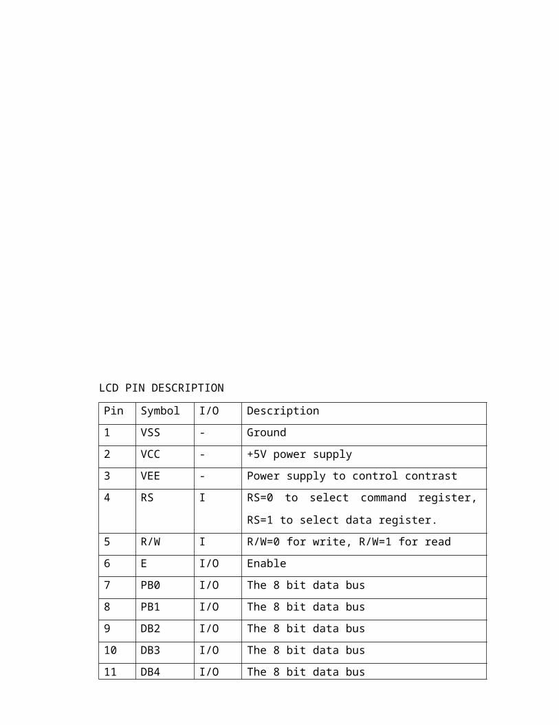
LCD PIN DESCRIPTION
Pin Symbol I/O Description
1 VSS - Ground
2 VCC - +5V power supply
3 VEE - Power supply to control contrast
4 RS I RS=0 to select command register, RS=1 to select
data register.
5 R/W I R/W=0 for write, R/W=1 for read
6 E I/O Enable
7 PB0 I/O The 8 bit data bus

8 PB1 I/O The 8 bit data bus
9 DB2 I/O The 8 bit data bus
10 DB3 I/O The 8 bit data bus
11 DB4 I/O The 8 bit data bus
12 DB5 I/O The 8 bit data bus
13 DB6 I/O The 8 bit data bus
14 DB7 I/O The 8 bit data bus
44780 BACKGROUND
The 44780 standard requires 3 control lines as well as either 4 or 8 I/O lines for the data
bus. The user may select whether the LCD is to operate with a 4-bit data bus or an 8-bit
data bus. If a 4-bit data bus is used the LCD will require a total of 7 data lines (3 control
lines plus the 4 lines for the data bus). If an 8-bit data bus is used the LCD will require a
total of 11 data lines (3 control lines plus the 8 lines for the data bus).
The three control lines are referred to as EN, RS, and RW.
The EN line is called "Enable." This control line is used to tell the LCD that you are
sending it data. To send data to the LCD, your program should make sure this line is low
(0) and then set the other two control lines and/or put data on the data bus. When the
other lines are completely ready, bring EN high (1) and wait for the minimum amount of
time required by the LCD datasheet (this varies from LCD to LCD), and end by bringing
it low (0) again.
The RS line is the "Register Select" line. When RS is low (0), the data is to be treated as
a command or special instruction (such as clear screen, position cursor, etc.). When RS
is high (1), the data being sent is text data which sould be displayed on the screen. For
example, to display the letter "T" on the screen you would set RS high.
The RW line is the "Read/Write" control line. When RW is low (0), the information on
the data bus is being written to the LCD. When RW is high (1), the program is
effectively querying (or reading) the LCD. Only one instruction ("Get LCD status") is a
read command. All others are write commands--so RW will almost always be low.
Finally, the data bus consists of 4 or 8 lines (depending on the mode of operation
selected by the user). In the case of an 8-bit data bus, the lines are referred to as DB0,
DB1, DB2, DB3, DB4, DB5, DB6, and DB7.

AN EXAMPLE HARDWARE CONFIGURATION
As we've mentioned, the LCD requires either 8 or 11 I/O lines to communicate with. For
the sake of this tutorial, we are going to use an 8-bit data bus--so we'll be using 11 of the
8051's I/O pins to interface with the LCD.
Let's draw a sample psuedo-schematic of how the LCD will be connected to the 8051.
As you can see, we've established a 1-to-1 relation between a pin on the 8051 and a line
on the 44780 LCD. Thus as we write our assembly program to access the LCD, we are
going to equate constants to the 8051 ports so that we can refer to the lines by their
44780 name as opposed to P0.1, P0.2, etc. Let's go ahead and write our initial equates:
DB0 EQU P1.0
DB1 EQU P1.1
DB2 EQU P1.2
DB3 EQU P1.3
DB4 EQU P1.4
DB5 EQU P1.5
DB6 EQU P1.6
DB7 EQU P1.7
EN EQU P3.7
RS EQU P3.6
RW EQU P3.5
DATA EQU P1

Having established the above equates, we may now refer to our I/O lines by their 44780
name. For example, to set the RW line high (1), we can execute the following
insutrction:
SETB RW
HANDLING THE EN CONTROL LINE
As we mentioned above, the EN line is used to tell the LCD that you are ready for it to
execute an instruction that you've prepared on the data bus and on the other control lines.
Note that the EN line must be raised/lowered before/after each instruction sent to the
LCD regardless of whether that instruction is read or write, text or instruction. In short,
you must always manipulate EN when communicating with the LCD. EN is the LCD's
way of knowing that you are talking to it. If you don't raise/lower EN, the LCD doesn't
know you're talking to it on the other lines.
Thus, before we interact in any way with the LCD we will always bring the EN line low
with the following instruction:
CLR EN
And once we've finished setting up our instruction with the other control lines and data
bus lines, we'll always bring this line high:
SETB EN
The line must be left high for the amount of time required by the LCD as specified in its
datasheet. This is normally on the order of about 250 nanoseconds, but check the
datasheet. In the case of a typical 8051 running at 12 MHz, an instruction requires 1.08
microseconds to execute so the EN line can be brought low the very next instruction.
However, faster microcontrollers (such as the DS89C420 which executes an instruction
in 90 nanoseconds given an 11.0592 Mhz crystal) will require a number of NOPs to
create a delay while EN is held high. The number of NOPs that must be inserted
depends on the microcontroller you are using and the crystal you have selected.
The instruction is executed by the LCD at the moment the EN line is brought low with a
final CLR EN instruction.
Programming Tip: The LCD interprets and executes our command at the instant the EN
line is brought low. If you never bring EN low, your instruction will never be executed.
Additionally, when you bring EN low and the LCD executes your instruction, it requires
a certain amount of time to execute the command. The time it requires to execute an

instruction depends on the instruction and the speed of the crystal which is attached to
the 44780's oscillator input.
CHECKING THE BUSY STATUS OF THE LCD
As previously mentioned, it takes a certain amount of time for each instruction to be
executed by the LCD. The delay varies depending on the frequency of the crystal
attached to the oscillator input of the 44780 as well as the instruction which is being
executed.
While it is possible to write code that waits for a specific amount of time to allow the
LCD to execute instructions, this method of "waiting" is not very flexible. If the crystal
frequency is changed, the software will need to be modified. Additionally, if the LCD
itself is changed for another LCD which, although 44780 compatible, requires more time
to perform its operations, the program will not work until it is properly modified.
A more robust method of programming is to use the "Get LCD Status" command to
determine whether the LCD is still busy executing the last instruction received.
The "Get LCD Status" command will return to us two tidbits of information; the
information that is useful to us right now is found in DB7. In summary, when we issue
the "Get LCD Status" command the LCD will immediately raise DB7 if it's still busy
executing a command or lower DB7 to indicate that the LCD is no longer occupied.
Thus our program can query the LCD until DB7 goes low, indicating the LCD is no
longer busy. At that point we are free to continue and send the next command.
Since we will use this code every time we send an instruction to the LCD, it is useful to
make it a subroutine. Let's write the code:
WAIT_LCD:
CLR EN ;Start LCD command
CLR RS ;It's a command
SETB RW ;It's a read command
MOV DATA,#0FFh ;Set all pins to FF initially
SETB EN ;Clock out command to LCD
MOV A,DATA ;Read the return value
JB ACC.7,WAIT_LCD ;If bit 7 high, LCD still busy
CLR EN ;Finish the command

CLR RW ;Turn off RW for future commands
RET
Thus, our standard practice will be to send an instruction to the LCD and then call our
WAIT_LCD routine to wait until the instruction is completely executed by the LCD.
This will assure that our program gives the LCD the time it needs to execute instructions
and also makes our program compatible with any LCD, regardless of how fast or slow it
is.
Programming Tip: The above routine does the job of waiting for the LCD, but were it to
be used in a real application a very definite improvement would need to be made: as
written, if the LCD never becomes "not busy" the program will effectively "hang,"
waiting for DB7 to go low. If this never happens, the program will freeze. Of course,
this should never happen and won't happen when the hardware is working properly. But
in a real application it would be wise to put some kind of time limit on the delay--for
example, a maximum of 256 attempts to wait for the busy signal to go low. This would
guarantee that even if the LCD hardware fails, the program would not lock up.
INITIALIZING THE LCD
Before you may really use the LCD, you must initialize and configure it. This is
accomplished by sending a number of initialization instructions to the LCD.
The first instruction we send must tell the LCD whether we'll be communicating with it
with an 8-bit or 4-bit data bus. We also select a 5x8 dot character font. These two
options are selected by sending the command 38h to the LCD as a command. As you
will recall from the last section, we mentioned that the RS line must be low if we are
sending a command to the LCD. Thus, to send this 38h command to the LCD we must
execute the following 8051 instructions:
CLR RS
MOV DATA,#38h
SETB EN
CLR EN
LCALL WAIT_LCD
Programming Tip: The LCD command 38h is really the sum of a number of option bits.
The instruction itself is the instruction 20h ("Function set"). However, to this we add the

values 10h to indicate an 8-bit data bus plus 08h to indicate that the display is a two-line
display.
We've now sent the first byte of the initialization sequence. The second byte of the
initialization sequence is the instruction 0Eh. Thus we must repeat the initialization code
from above, but now with the instruction. Thus the the next code segment is:
CLR RS
MOV DATA,#0Eh
SETB EN
CLR EN
LCALL WAIT_LCD
Programming Tip: The command 0Eh is really the instruction 08h plus 04h to turn the
LCD on. To that an additional 02h is added in order to turn the cursor on.
The last byte we need to send is used to configure additional operational parameters of
the LCD. We must send the value 06h.
CLR RS
MOV DATA,#06h
SETB EN
CLR EN
LCALL WAIT_LCD
Programming Tip: The command 06h is really the instruction 04h plus 02h to configure
the LCD such that every time we send it a character, the cursor position automatically
moves to the right.
So, in all, our initialization code is as follows:
INIT_LCD:
CLR RS
MOV DATA,#38h
SETB EN
CLR EN
LCALL WAIT_LCD
CLR RS
MOV DATA,#0Eh
SETB EN
CLR EN
LCALL WAIT_LCD
CLR RS
MOV DATA,#06h
SETB EN
CLR EN
LCALL WAIT_LCD
RET
Having executed this code the LCD will be fully initialized and ready for us to send
display data to it.
CLEARING THE DISPLAY
When the LCD is first initialized, the screen should automatically be cleared by the
44780 controller. However, it's always a good idea to do things yourself so that you can
be completely sure that the display is the way you want it. Thus, it's not a bad idea to
clear the screen as the very first opreation after the LCD has been initialiezd.
An LCD command exists to accomplish this function. Not suprisingly, it is the
command 01h. Since clearing the screen is a function we very likely will wish to call
more than once, it's a good idea to make it a subroutine:
CLEAR_LCD:
CLR RS
MOV DATA,#01h
SETB EN
CLR EN
LCALL WAIT_LCD
RET
How that we've written a "Clear Screen" routine, we may clear the LCD at any time by
simply executing an LCALL CLEAR_LCD.
Programming Tip: Executing the "Clear Screen" instruction on the LCD also positions
the cursor in the upper left-hand corner as we would expect.
WRITING TEXT TO THE LCD
Now we get to the real meat of what we're trying to do: All this effort is really so we can
display text on the LCD. Really, we're pretty much done.
Once again, writing text to the LCD is something we'll almost certainly want to do over
and over--so let's make it a subroutine.
WRITE_TEXT:
SETB RS
MOV DATA,A
SETB EN
CLR EN
LCALL WAIT_LCD
RET
The WRITE_TEXT routine that we just wrote will send the character in the accumulator
to the LCD which will, in turn, display it. Thus to display text on the LCD all we need to
do is load the accumulator with the byte to display and make a call to this routine. Pretty
easy, huh?
A "HELLO WORLD" PROGRAM
Now that we have all the component subroutines written, writing the classic "Hello
World" program--which displays the text "Hello World" on the LCD is a relatively
trivial matter. Consider:
LCALL INIT_LCD
LCALL CLEAR_LCD
MOV A,#'H'
LCALL WRITE_TEXT
MOV A,#'E'
LCALL WRITE_TEXT
MOV A,#'L'
LCALL WRITE_TEXT
MOV A,#'L'
LCALL WRITE_TEXT
MOV A,#'O'

LCALL WRITE_TEXT
MOV A,#' '
LCALL WRITE_TEXT
MOV A,#'W'
LCALL WRITE_TEXT
MOV A,#'O'
LCALL WRITE_TEXT
MOV A,#'R'
LCALL WRITE_TEXT
MOV A,#'L'
LCALL WRITE_TEXT
MOV A,#'D'
LCALL WRITE_TEXT
The above "Hello World" program should, when executed, initialize the LCD, clear the
LCD screen, and display "Hello World" in the upper left-hand corner of the display.
CURSOR POSITIONING
The above "Hello World" program is simplistic in the sense that it prints its text in the
upper left-hand corner of the screen. However, what if we wanted to display the word
"Hello" in the upper left-hand corner but wanted to display the word "World" on the
second line at the tenth character? This sounds simple--and actually, it is simple.
However, it requires a little more understanding of the design of the LCD.
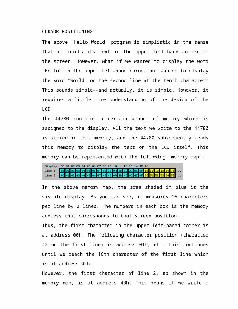
The 44780 contains a certain amount of memory which is assigned to the display. All
the text we write to the 44780 is stored in this memory, and the 44780 subsequently
reads this memory to display the text on the LCD itself. This memory can be represented
with the following "memory map":
In the above memory map, the area shaded in blue is the visible display. As you can see,
it measures 16 characters per line by 2 lines. The numbers in each box is the memory
address that corresponds to that screen position.

Thus, the first character in the upper left-hanad corner is at address 00h. The following
character position (character #2 on the first line) is address 01h, etc. This continues until
we reach the 16th character of the first line which is at address 0Fh.
However, the first character of line 2, as shown in the memory map, is at address 40h.
This means if we write a character to the last position of the first line and then write a
second character, the second character will not appear on the second line. That is
because the second character will effectively be written to address 10h--but the second
line begins at address 40h.
Thus we need to send a command to the LCD that tells it to position the cursor on the
second line. The "Set Cursor Position" instruction is 80h. To this we must add the
address of the location where we wish to position the cursor. In our example, we said we
wanted to display "World" on the second line on the tenth character position.
Referring again to the memory map, we see that the tenth character position of the
second line is address 4Ah. Thus, before writing the word "World" to the LCD, we must
send a "Set Cursor Position" instruction--the value of this command will be 80h (the
instruction code to position the cursor) plus the address 4Ah. 80h + 4Ah = C4h. Thus
sending the command C4h to the LCD will position the cursor on the second line at the
tenth character position:
CLR RS
MOV DATA,#0C4h
SETB EN
CLR EN
LCALL WAIT_LCD
The above code will position the cursor on line 2, character 10. To display "Hello" in the
upper left-hand corner with the word "World" on the second line at character position 10
just requires us to insert the above code into our existing "Hello World" program. This
results in the following:
LCALL INIT_LCD
LCALL CLEAR_LCD
MOV A,#'H'
LCALL WRITE_TEXT
MOV A,#'E'

LCALL WRITE_TEXT
MOV A,#'L'
LCALL WRITE_TEXT
MOV A,#'L'
LCALL WRITE_TEXT
MOV A,#'O'
LCALL WRITE_TEXT
CLR RS
MOV DATA,#0C4h
SETB EN
CLR EN
LCALL WAIT_LCD
MOV A,#'W'
LCALL WRITE_TEXT
MOV A,#'O'
LCALL WRITE_TEXT
MOV A,#'R'
LCALL WRITE_TEXT
MOV A,#'L'
LCALL WRITE_TEXT
MOV A,#'D'
LCALL WRITE_TEXT
SUMMARY
This tutorial has presented the underlying concepts of programming an LCD display.
Obviously it has not addresses all issues. The 44780 LCD controller offers many other
functions which are accessed using other commands, and some of the commands already
presented include other options that were not discussed here. However, this tutorial
should get you going in the right direction.
OPTOCOUPLER

OPTO-COUPLER :- it has one IR LED and a photo- transistor. One pin of the LED is
connected to the MCU to get a signal (0 or 1) and the pin is given ground. When the
signal from the MCU is 0, then LED emits light. This light will turn on the npn
transistor. Collector of the transistor is grounded. Emitter is connected to the pnp
transistor whose collector is connected to Vcc and emitter to the relay.
P in npn transistor means 1 and n means 0.
RELAY
NC (normally closed)
Phase NO (normally open)
vcc
One point of the relay is given to phase and that point is connected to NC point. VCC is
connected to the coil the relay. When vcc is given the coil gets magnetized and slowly
phase is connected to NO point which is further connected to the device to be operated
by the relay.Neutral must be given to the device.
CURRENT INFRARED COMMUNICATION SYSTEMS
At present, most infrared links are of the directed-LOS or hybrid-LOS designs. The low
path loss of these designs minimizes the transmitter power requirement and permits the
use of a simple, low-cost receiver. Typically, these links transmit using a single light-
emitting diode (LED), which emits an average power of several tens of mW that is
concentrated within a semi angle of 15to 30The LED emission wavelength
typically lies between 850 and 950 nm. This wavelength matches the responsivity peak
of the silicon positive-intrinsic-negative (p-i-n) photodiode. The wavelength band
between about 780 and 950 nm is presently the best choice for most applications of
Device

infrared wireless links, due to the availability of low-cost LEDs and laser diodes (LDs),
and because it coincides with the peak responsivity of inexpensive, low-capacitance
silicon photodiodes. Infrared radiation a type of invisible radiation for which the
wavelengths are longer and frequency lower than those for visible radiation
A light emitting diode (LED) is a semiconductor device which emits visible, infrared or
ultraviolet radiation due to flow of electric current through it. Essentially it is a p-n
junction device with p- and n-regions made from the same or different semiconductors.
The color of the emitted light is determined by the energy of the photons, and in general,
this energy is usually approximately equal to the energy band gap Eg of the
semiconductor material in the active region of the LED. III-V semiconductors such as
GaAs, GaP, AlGaAs, InGaP, GaAsP, GaAsInP, AlInGaP, etc. are the common
constituents of an LED. However, which materials would be used for which LED
depends on the choice of color, performance and cost. Operating currents at a forward
voltage of about 2 V are usually in the range of 1-50 mA. Infrared (IR) and red emission
Eg should be less than 2 eV, a range possessed by GaAs AlGaAs and GaAsP.
The performance of LEDs is typically in the range of 1 to 10 W-1, although performance
as high as 20 W-1 can also be achieved. This is comparable with 10-15 W-1
performance of an incandescent bulb. LEDs are very suitable for room illumination
because, at the lower level, they can operate even at less than 0.1 W. Parallel to the
development of visible LEDs infrared (IR) LEDs also attracted interests. Instead of
being detected by eyes, these LEDs are detected by photodiodes or phototransistors.
Therefore, IR LEDs can function as important tools for transmitting data. How fast these
data will be transmitted depends on the switching speed of the IR LEDs. Therefore, this
switching speed is quite unimportant for visible LEDS, this is an important performance
parameter for IR LEDs.
The IR Light Emitter
Principle of Operation
Because they emit at wavelengths which provide a close match to the peak spectral
response of silicon photodetectors, both GaAs and GaAlAs. There are many off-the-
shelf, commercially available, IR LED emitters that can be used for a discrete infrared

transceiver circuit design. It should be mentioned here that there are also a number of
integrated transceivers that the designer can choose as well. In general, there are four
characteristics of IR emitters that designers have to be wary of:
Rise and Fall Time
Emitter Wavelength
Emitter Power
Emitter Half-angle
Fig 3.12: Wavelength vs. Radiant Power
Description
In this system IR LED used is The QED233 / QED234 which is a 940 nm GaAs /
AlGaAs LED encapsulated in a clear untinted, plastic T-1 3/4 package.

Picture 3.3: IR Led Fig 3.13: LED Schematic
QED234 Features
Wavelength=940nm
Chip material =GaAs with AlGaAs window
Package type: T-1 3/4 (5mm lens diameter)
Matched Photo sensor: QSD122/123/124, QSE 973.
Medium Emission Angle, 40°
High Output Power
Package material and color: Clear, untinted, plastic
Ideal for remote control applications
Semiconductor Light Detectors
Energy entering a semiconductor crystal excites electrons to higher levels, leaving
behind "holes". These electrons and "holes" can recombine and emit photons, or they
can move away from one another and form a current. This is the basics of semiconductor
light detectors. The basic optical receiver converts the modulated light coming from the
space back in to a replica of the original signal applied to the transmitter.
Types of optical detector
P-N photodiode
P-I-N photodiode
Anode Cathode

Avalanche photodiode
In P-N photodiode, electron hole pairs are created in the depletion region of a p-n
junction in proportion to the optical power. Electrons and holes are swept out by the
electric field, leading to a current. In P-I-N photodiode, electric field is concentrated in a
thin intrinsic layer. In avalanche photodiode, like P-I-N photodiodes, but have an
additional layer in which an average of M secondary electron –hole pairs are generated
through impact ionization for each primary pair. Photodiodes usually have a large
sensitive detecting area that can be several hundreds microns in diameter.
The IR Light Detector
The most common device used for detecting light energy in the standard data stream is a
photodiode, Photo transistors are not typically used in IrDA standard-compatible
systems because of their slow speed. Photo transistors typically have ton/toff of 2 µs or
more. A photo transistor may be used, however, if the data rate is limited to 9.6 kb with
a pulse width of 19.5 µs. A photodiode is packaged in such a way as to allow light to
strike the PN junction.
Fig 3.14: Characteristic Curve of a Reverse Biased Photodiode
In infrared applications, it is common practice to apply a reverse bias to the device.
Refer to Figure 3.17 for a characteristic curve of a reverse biased photodiode. There will
be a reverse current that will vary with the light level. Like all diodes, there is an

intrinsic capacitance that varies with the reverse bias voltage. This capacitance is an
important factor in speed.
Description
The QSE973 is a silicon PIN photodiode encapsulated in an infrared transparent, black,
plastic T092 package.
1 2
+_
Picture 3.4: IR Photodiode Fig 3.15 Reverse Bias Photodiode
QSE 973 Features
Daylight filter
T092 package
PIN photodiode
Recepting angle 90°
Chip size = .1072 sq. inches (2.712 sq. mm)
Link Distance
To select an appropriate IR photo-detect diode, the designer must keep in mind the
distance of communication, the amount of light that may be expected at that distance and
the current that will be generated by the photodiode given a certain amount of light
energy. The amount of light energy, or irradiance that is present at the active-input
interface is typically given in µW/cm2. This is a convenient scale of light flux [36].
Transmitter Circuit
AnodeCathode

The Output from the microcontroller is fed to the optical transmitter circuit. The output
is given to the n-p-n transistor BC -547 .A high signal from the microcontroller is given
to the transistor act as a closed switch results the ground at emitter reach at the collector
of the transistor and the LED emits. Similarly a low output signal from the
microcontroller make the transistor off and LED wouldn’t emit. So when the voltage
applied to LED it emits the light in the range of IR. As the current specification of LED
can not be fulfilled by the microcontroller, voltage specification may be fulfilled, so
need of the driver circuitry.
Fig 3.22: Optical Transmitter Circuit
OPTIC- ELECTRO MODULE
This module converts the light energy in to electrical signal. It recovers the electronic
signal from the light at the other end of the space by using photo detector.
Receiver Circuit
The light pulses are coming from the fiber optic cable. The photo detector detects the
light pulses and converted in to electrical form. Photodiode work on reverse biased.
when light fall on photodiode ,Vcc at the cathode reach at the input of 555 timer and
allow it to produce the single pulse at the output . The output of the 555 timer make the
npn transistor on . the output of the transistor make relay’s coil magnetized and alow it
to trigger.

APPENDIX
PROGRAM DESCRIPTION:
#define DATA P1
#define RS P35
#define RW P36

#define E P37
#include<lcdrout.h>
#define in1 P20 //entry intruder
#define in3 P21 //Exit intruder
#define buzz P26 //Don't connect to p2
#define st1 P22
#define st2 P23
#define st3 P24
#define st4 P25
void open() //funtion for open the door
{
unsigned char count=6;
while(count>0)
{
st1=0;
st2=st3=st4=1;
ms_delay(50);
st2=0;
st1=st3=st4=1;
ms_delay(50);
st3=0;
st2=st1=st4=1;
ms_delay(50);
st4=0;
st2=st3=st1=1;
ms_delay(50);
st4=st2=st3=st1=1;
count--;
}
}
void close()
{
unsigned char count=6;
while(count>0)
{
st4=0;
st2=st3=st1=1;
ms_delay(50);
st3=0;
st1=st2=st4=1;
ms_delay(50);
st2=0;
st3=st1=st4=1;
ms_delay(50);
st1=0;
st2=st3=st4=1;
ms_delay(50);
st4=st2=st3=st1=1;
count--;
}
}
void main()
{
unsigned int i=0,max=0;
lcd_initialize();
ACC=0x01;
lcd_cmd();
ACC=0x83;
lcd_cmd();
lcd_display("Advanced",8);
ACC=0xc0;
lcd_cmd();
lcd_display("Car Parking",11);

secdelay(3);
ACC=0x01;
lcd_cmd();
max=7;
while(1)
{
if(in1==0)
{
buzz=0;
ms_delay(100);
buzz=1;
if(i==max)
{
lcd_display("No Space",8);
buzz = 0;
secdelay(3);
buzz = 1;
}
else
{
i=i+1;
lcd_display("Opening...",10);
secdelay(1);
open();
secdelay(5);
ACC=0x83;
lcd_cmd();
lcd_display("Closing...",10);
close();
secdelay(1);
}
if(in3==0)

{
buzz=0;
ms_delay(100);
buzz=1;
i=i-1;
}
}
ACC=0x80;
lcd_cmd();
lcd_display("No of Vehicles:-",16);
ACC=0xc6;
lcd_cmd();
displaypval(i)
}
}