filter design for interference cancellation for wide and ......filter design for interference...
TRANSCRIPT

Filter Design for Interference Cancellation for Wide and Narrow Band RF
Systems
MohammadReza Zargarzadeh
Thesis submitted to the faculty of the Virginia Polytechnic Institute and State University in
partial fulfillment of the requirements for the degree of
Master of Science
In
Electrical Engineering
Dong S. Ha, Chair
Luke F. Lester
Sanjay Raman
April 26, 2016
Blacksburg, VA
Keywords: band pass filter, band stop filter, notch, Volterra series, interference cancellation,
software defined radios, Q-enhanced filters, feedback interference cancellation, frequency
tunable, bandwidth tunable

Filter Design for Interference Cancellation for Wide and Narrow Band RF Systems
MohammadReza Zargarzadeh
Scholarly Abstract In radio frequency (RF), filtering is an essential part of RF transceivers. They are employed
for different purposes of band selection, channel selection, interference cancellation, image
rejection, etc. These are all translated in selecting the wanted signal while mitigating the rest. This
can be performed by either selecting the desired frequency range by a band pass filter or rejecting
the unwanted part by a band stop filter.
Although there has been tremendous effort to design RF tunable filters, there is still lack
of designs with frequency and bandwidth software-tuning capability at frequencies above 4 GHz.
This prevents the implementation of Software Defined Radios (SDR) where software tuning is a
critical part in supporting multiple standards and frequency bands. Designing a tunable integrated
filter will not only assist in realization of SDR, but it also causes an enormous shrinkage in the
size of the circuit by replacing the current bulky off-chip filters. The main purpose of this research
is to design integrated band pass and band stop filters aimed to perform interference cancellation.
In order to do so, two systems are proposed for this thesis. The first system is a band pass
filter capable of frequency and band with tuning for C band frequency range (4-8 GHz) and is
implemented in 0.13 µm BiCMOS technology. Frequency tunability is accomplished by using a
variable capacitor (varactor) and bandwidth tuning is carried out by employing a negative
transconductance cell to compensate for the loss of the elements. Additional circuitry is added to
the band pass filter to enhance the selectivity of the filter. The second system is a band stop filter
(notch) with the same capability as the band pass filter in terms of tuning. This system is
implemented in C band, similar to its band stop counterpart and is capable of tuning its depth by
using a negative transconductance in an LC tank. A negative feedback is added to the circuit to
improve the bandwidth. While implemented in the same process as the band pass filter, it only
employs CMOS transistors since it is generally more attractive due to its lower cost and scalability.
Both of the systems mentioned use a varactor for changing the center frequency which is a
nonlinear element. Therefore, the nonlinearity of it is modelled using two different methods of
nonlinear feedback and Volterra series in order to gain further understanding of the nonlinear
process taking place in the LC tank. After the validation of the models proposed using Cadence
Virtuoso simulator, two methods of design and tuning are suggested to improve the linearity of the
system.
After post layout-extraction, the band pass filter is capable of Q tuning in the range of 3 to
270 and higher. With the noise figure of 10 to 14 dB and input 1-dB compression point as high as
2 dBm, the system shows a reasonably good performance along its operating frequency of 4 to 8
GHz. The band stop filter which is designed in the same frequency band can achieve better than
55 dB of rejection with the noise figure of 6.7 to 8.8 dB and 1-dB compression point of -4 dBm.
With the power consumption of 39 to 70 mW, the band stop filter can be used in a low power
receiver to suppress unwanted signals. The technique used in the band stop filter can be applied to
higher frequency ranges if the circuit is implemented in a more advanced silicon technology.

Implementing the mentioned filters in a receiver along with other elements of low noise amplifiers,
mixers, etc. would be a major step toward full implementation of SDR systems. Studying the
linearity theory of varactors would help future designers identify the sources of nonlinearity and
suggest more efficient tuning techniques to improve the linearity of RF electronic systems.
Filter Design for Interference Cancellation for Wide and Narrow Band RF Systems
MohammadReza Zargarzadeh
General Audience Abstract Wireless systems are becoming more widespread every day. These systems consist of
mobile phones, laptops with wireless capabilities, wearable devices, etc. The ultimate goal of such
systems is to replace current bulky and expensive wires and provide mobility and more flexibility.
That requires a robust wireless system capable of supporting different standards and applications.
The mentioned requirements can be achieved by implementing Software Defined Radios (SDR).
An SDR is a wireless system which can be tuned to support different wireless standards using a
software. One key element of an SDR is a Radio Frequency (RF) filter which is responsible for
selecting the desired frequency band to receive useful information depending on the application
while rejecting the unwanted signals.
Although there has been designs to realize SDR, most of them are using separate circuits
as RF filters. Using separate off-chip filters will significantly increase the overall size of the circuit.
Moreover, such filters have less tunable parameters compared to their integrated filters
counterpart. An integrated filter is a circuit on the same chip as the rest of the radio. Using an
integrated filter can significantly reduce the overall size of the system. However, integrated filters
often show lower performance compared to off-chip filters. In order to achieve a performance
comparable to non-integrated filters, new electronic circuit methods need to be developed to
enhance the performance of the filter. The main goal of this research is to introduce novel
integrated filters with outstanding performance.
After designing the filters and running post layout simulations, the circuit shows promising
performance. Based on the simulation results, it can be proven that it is feasible to design an
integrated filter with a wide range of tunable parameters with the potential to be integrated with
the rest of the SDR. Successful implementation of the system in integrated circuit level can pave
the way for the next generation of wireless systems with the capability of supporting multiple
applications by programming the device without changing the hardware.

v
To my wife, Zahra and my parents

vi
Acknowledgement
I would like to thank my committee chair, Professor Dong S. Ha for his assistance and
mentorship. Professor Luke F. Lester’s support has been a key part in my master’s defense. I would
also like to thank Professor Sanjay Raman for being part of my advisory committee. Without the
help and support of my committee members, it would not have been possible to accomplish this
work for which I will always be grateful.
I am thankful to Professor Kwang-Jin Koh for his financial support and technical comments
and recommendations on my designs and models throughout this work.
I would like to thank my colleagues in MICS RFIC lab for all of their comments and
suggestions on my work. It was a great pleasure working with them during my master’s study.
Also, many thanks to other members of MICS group.
I am beyond grateful to my soulmate and wife, Zahra for her love and encouragement. Her
love has always been a motivation for me. She has never stopped being supportive of my decisions
and I am always grateful for her continuous patience and understanding through all the difficult
times of graduate school. This thesis would have never been completed without her endless
friendship and love.
Lastly, I am extremely grateful to my parents, Mohsen and Sepideh for their unconditional
support and great advice in my entire life.

vii
Table of Contents
Chapter 1. Introduction ................................................................................................................... 1
1.1 Motivation ........................................................................................................................ 1
1.2 Scope of the Proposed Research ...................................................................................... 1
1.3 Contributions of the Proposed Research .......................................................................... 2
1.4 Organization of the Thesis ............................................................................................... 3
Chapter 2. Preliminaries.................................................................................................................. 4
2.1 Basic Concepts ................................................................................................................. 4
2.1.1. Filtering in RF Transceivers .................................................................................. 4
2.1.2. Performance Metrics ............................................................................................. 6
2.2 Filter Topologies .............................................................................................................. 9
2.2.1. Passive Filters ........................................................................................................ 9
2.2.2. Switched Capacitor Filters .................................................................................. 15
2.2.3. Active Filters ....................................................................................................... 16
2.3 Literature Review ........................................................................................................... 17
2.4 Chapter Summary ........................................................................................................... 19
Chapter 3. Proposed Designs ........................................................................................................ 21
3.1 Design Requirements ..................................................................................................... 21
3.2 Block Diagram ............................................................................................................... 22
3.2.1. Band-Pass Filter .................................................................................................. 22
3.2.2. Band-Stop Filter .................................................................................................. 25
3.3 Circuit Details ................................................................................................................ 28
3.3.1. Band-Pass Filter .................................................................................................. 28
3.3.2. Band-Stop Filter .................................................................................................. 34
3.4 Linearity Theory ............................................................................................................. 39
3.4.1. Nonlinear Feedback Model ................................................................................. 40
3.4.2. Volterra Series Model ......................................................................................... 45
3.5 Chapter Summary ........................................................................................................... 49
Chapter 4. Implementation............................................................................................................ 50
4.1 Schematic Simulations ................................................................................................... 50
4.1.1. S Parameter Simulation ....................................................................................... 50
4.1.2. Noise Simulation ................................................................................................. 58
4.1.3. Linearity Simulation ............................................................................................ 60

viii
4.2 Layout of the Designs .................................................................................................... 62
4.2.1. Band Pass Filter Layout ...................................................................................... 62
4.2.2. Band Stop Filter Layout ...................................................................................... 66
4.3 Post Layout Simulations................................................................................................. 68
4.3.1. S Parameter Simulation ....................................................................................... 68
4.3.2. Noise Simulation ................................................................................................. 74
4.3.3. Linearity Simulation ............................................................................................ 75
4.3.4. Power Consumption ............................................................................................ 76
4.4 Performance Comparison ............................................................................................... 77
4.5 Chapter Summary ........................................................................................................... 78
Chapter 5. Conclusion ................................................................................................................... 79
References ..................................................................................................................................... 80

ix
List of Figures
Figure 2.1 Dual IF receiver architecture ......................................................................................... 4 Figure 2.2 Heterodyne transmitter architecture .............................................................................. 5 Figure 2.3 A transceiver with duplexer supporting FDMA ............................................................ 6 Figure 2.4 band pass filter (left) and band stop filter (right) frequency response and their
performance characteristics ............................................................................................................ 7 Figure 2.5 1dB-Compression point (left) and two tone test (right) for third order intercept point
calculation ....................................................................................................................................... 8 Figure 2.6 First order low pass (left) and high pass (right) filters ................................................ 10 Figure 2.7 Thevenin (left) and Norton (right) second order band pass filters .............................. 11 Figure 2.8 The effect of finite Q of the elements on the overall Q of the system ........................ 11 Figure 2.9 Thevenin (left) and Norton (right) second order band stop filters .............................. 12
Figure 2.10 Block diagram of an N-path filter architecture.......................................................... 13 Figure 2.11 Conceptual N-path frequency plots for a band pass filter ......................................... 14
Figure 2.12 N-path circuit diagram (left) and its simplified circuit (right) .................................. 15 Figure 2.13 Switched Capacitor basic building block .................................................................. 16 Figure 2.14 Interference Cancellation Techniques – Frequency translational filtering (left),
Feedforward filtering (middle) and Feedback technique (right)................................................... 19 Figure 3.1 Synthesized notch based feedback interference cancelling system ............................. 22
Figure 3.2 Interference cancelling system based on an LC notch ................................................ 24 Figure 3.3 Proposed system of this thesis based on feedback cancellation technique ................. 24 Figure 3.4 An ideal transconductor with an impedance in its common terminal ......................... 25
Figure 3.5 Proposed notch ............................................................................................................ 26 Figure 3.6 Feedback assisted notch filter ...................................................................................... 27
Figure 3.7 Final version of the proposed feedback based notch consisting of a low noise amplifier
(LNA) to reduce the noise figure .................................................................................................. 27
Figure 3.8 Darlington negative resistance .................................................................................... 29 Figure 3.9 Q enhanced band pass filter using both voltage driven and current driven configuration
and Darlington negative gm cell to enhanced the Q ..................................................................... 30
Figure 3.10 Buffer and gain stage in feedback ............................................................................. 31 Figure 3.11 post VGA buffers in feedback ................................................................................... 32
Figure 3.12 Notch in the feedback ................................................................................................ 33 Figure 3.13 Output buffer of the feedback path ............................................................................ 34 Figure 3.14 Preliminary CMOS notch .......................................................................................... 35
Figure 3.15 Proposed basic circuit of the notch ............................................................................ 36 Figure 3.16 Proposed LNA schematic .......................................................................................... 37 Figure 3.17 The complete schematic of the proposed notch ........................................................ 38 Figure 3.18 Linear and nonlinear coefficients of a varactor ......................................................... 41
Figure 3.19 Varactor nonlinear modeling of an LC tank .............................................................. 41 Figure 3.20 The nonlinear feedback model of the varactor .......................................................... 42 Figure 3.21 The nonlinear feedback model of the tank ................................................................ 44 Figure 3.22 First order kernel circuit ............................................................................................ 46 Figure 3.23 Second order kernel circuit ........................................................................................ 46 Figure 3.24 Third order kernel circuit ........................................................................................... 47

x
Figure 3.25 verification of nonlinear model proposed in this work ............................................. 48 Figure 3.26 Dual varactor control simulation ............................................................................... 49 Figure 4.1 simulating hybrid coupler using an ideal transformer ................................................. 51 Figure 4.2 Schematic matching simulation of the band pass filter ............................................... 52
Figure 4.3 Schematic matching simulation of the band stop filter ............................................... 53 Figure 4.4 K stability factor for low frequency (left), mid frequency (middle) and high frequency
(right) of the band pass filter ......................................................................................................... 54 Figure 4.5 K stability factor for the band stop filter ..................................................................... 54 Figure 4.6 Output response of the band pass filter for low Q cases of low frequency (left), mid
frequency (middle) and high frequency (right) ............................................................................. 55 Figure 4.7 Output response of the band pass filter for high Q cases of low frequency (left), mid
frequency (middle) and high frequency (right) ............................................................................. 56
Figure 4.8 Output response of the band stop filter for low Q cases of low frequency (left), mid
frequency (middle) and high frequency (right) ............................................................................. 56 Figure 4.9 Output response of the band stop filter for high Q cases of low frequency (left), mid
frequency (middle) and high frequency (right) ............................................................................. 57 Figure 4.10 Notch depth tuning .................................................................................................... 57
Figure 4.11 Noise Figure of the band pass filter for low Q cases of low frequency (left), mid
frequency (middle) and high frequency (right) ............................................................................. 58 Figure 4.12 Noise Figure of the band pass filter for high Q cases of low frequency (left), mid
frequency (middle) and high frequency (right) ............................................................................. 59 Figure 4.13 Schematic simulation of the Noise Figure of the band stop filter for open loop and
closed loop cases ........................................................................................................................... 60 Figure 4.14 1-dB compression point simulation of the band pass filter ....................................... 61
Figure 4.15 1-dB compression point simulation of the band stop filter ....................................... 62 Figure 4.16 Floor planning of the band pass filter layout ............................................................. 64
Figure 4.17 The layout of the buffer and gain stage of the feedback path ................................... 64 Figure 4.18 The layout of the LC tank of the notch...................................................................... 65 Figure 4.19 Band pass filter final layout ....................................................................................... 65
Figure 4.20 Floor planning of the band pass filter layout ............................................................. 67 Figure 4.21 Final layout of the band stop filter ............................................................................ 68
Figure 4.22 Post layout matching simulation of the band pass filter ............................................ 69 Figure 4.23 Post layout matching simulation of the band stop filter ............................................ 69
Figure 4.24 K stability factor for low frequency (left), mid frequency (middle) and high frequency
(right) of the band pass filter in post layout simulation ................................................................ 70 Figure 4.25 K stability factor for the band stop filter after post layout simulations ..................... 71 Figure 4.26 Output response of the band pass filter for low Q cases of low frequency (left), mid
frequency (middle) and high frequency (right) after post layout .................................................. 71 Figure 4.27 Output response of the band pass filter for high Q cases of low frequency (left), mid
frequency (middle) and high frequency (right) after post layout .................................................. 72
Figure 4.28 Output response of the band stop filter for low Q cases of low frequency (left), mid
frequency (middle) and high frequency (right) for post layout .................................................... 72 Figure 4.29 Output response of the band stop filter for high Q cases of low frequency (left), mid
frequency (middle) and high frequency (right) for post layout .................................................... 73 Figure 4.30 Notch depth tuning for post layout ............................................................................ 73

xi
Figure 4.31 Noise Figure of the band pass filter for low Q cases of low frequency (left), mid
frequency (middle) and high frequency (right) for post layout .................................................... 74 Figure 4.32 Noise Figure of the band pass filter for high Q cases of low frequency (left), mid
frequency (middle) and high frequency (right) for post layout .................................................... 74
Figure 4.33 Schematic simulation of the Noise Figure of the band stop filter for open loop and
closed loop cases for layout .......................................................................................................... 75 Figure 4.34 1-dB compression point simulation of the band pass filter for post layout ............... 76 Figure 4.35 1-dB compression point of the band stop filter for post layout ................................. 76

xii
List of Tables
Table 1 Comparison table for the state of the art band stop filters ............................................... 77 Table 2 Comparison table for the state of the art band pass filters ............................................... 78

1
1 Chapter
Introduction
1.1 Motivation software defined radio (SDR) is one of the trending topics in wireless communication. SDR
necessitates that a wireless transceiver supports multiple wireless standards in order to adapt itself
to the new environments required by the software. This can be translated into a single transceiver
capable of transmitting and receiving in different frequency bands. While the existing wireless
systems employ separate integrated circuits (IC) for each wireless standards, integrating the whole
system into a single chip with one transceiver module will significantly shrink the size of the
system. While achieving the mentioned goal has its own challenges which will be later discussed,
the issue of coexistence with other wireless standards imposes stricter design requirements. [1]
There is an increasing demand for high-data rate transfer turning into higher bandwidth
requirement. Consequently, the frequency spectrum is subjected to more traffic and interferers.
With the advent of Internet of Things (IoT) and 5th generation mobile networks (5G) expected the
be introduced commercially by 2020 [2], the issue of busy spectrum and strong interferers will
become even more detrimental. Strong blockers cause significant degradation in the sensitivity
and desensitization of the receiver, ultimately reducing the dynamic range of the system.
Therefore, proper filtering is required to suppress unwanted signals in order to sustain the normal
operation of the system. Existing off-chip filters can offer sufficient out of band rejection.
However, they lack the ability to tune to different frequencies and their out of band rejection cannot
be altered. Moreover, using off-chip components will increase the area of the system.
Consequently, an on-chip filter with tuning capability would revolutionize traditional RF systems
by moving them towards modern software tunable systems.
The goal of this research project is to address the issues of tunability and integrability by
developing a new filter structure. Additionally, the theoretical study of the linearity of the proposed
system is conducted to gain a better understanding of the system’s behavior.
1.2 Scope of the Proposed Research The main role of a filter in an electronic system is to suppress unwanted signals while
maintaining a linear relationship for the desired ones in order to avoid distortion. Previous active
filter designs suffer from low dynamic range due to the fact that using amplifiers as the cornerstone
of the filter limits the linearity of the system since the amplifier itself is a nonlinear element [3].
There have recently been efforts to improve the linearity of the filter with the assistance of passive
techniques such as N-path filter [4]. Although the mentioned technique would address the issue of
linearity, implementing it in the frequency of higher than 2 GHz has not been reported yet.

2
The design proposed by Laya Mohammadi in [5] aims to improve the dynamic range while
implementing a tunable filter along a wide frequency range for frequencies higher than 2 GHz up
to 4 GHz. The structure of the filter is based on a simple second order LC filter. However, due to
the low Quality factor (Q) of the elements especially the inductors, a Q-enhancement technique is
employed to improve the selectivity of the filter. With the assistance of the technique, Q can be
adjusted from 10 to 100 and higher. A wide continuous tuning range of 2x is achieved by using a
varactor to control the center frequency of the filter.
While Mohammadi’s design brings about a wide range of selectivity (Q) along with a broad
tuning range, it has performance limitations which need to be addressed. First, the filter employs
a negative transconductance (gm) cell in order to compensate the loss of the LC tank and enhance
the selectivity (Q). It turns out the technique will significantly downgrade the noise figure for high
Q where the noise penalty introduced by the gm cell notably contributes to the overall noise of the
system. In the system, the noise figure can be as low as 10 dB for Q of 20 and it is increased to 20
dB for Q of 100. Second, the capacitance of the varactor used in the filter for frequency tuning is
sensitive to the voltage across its terminals. In the ideal small signal situation, the capacitance is
assumed to be constant with the value determined by its bias point. However, as the voltage
increases, the assumption will no longer be valid and the system becomes more nonlinear. This
thesis aims to introduce systems which can handle bottlenecks of noise and linearity while
retaining a wide tuning range and Q. Moreover, the theory behind the nonlinearity imposed by the
varactor will be studied and investigated.
1.3 Contributions of the Proposed Research Two separate interference cancelling systems have been designed for this research, a band
pass filter to select the desired frequency band and a band stop (notch) filter aimed at rejecting
strong interferers. Both circuits benefit from feedback principles to achieve the desired
performance. The major design target of both systems is to break the trade-off between linearity
and noise by improving one without altering the other. The research contributions of the thesis are
as follows.
First, Mohammadi’s circuit is studied and the nonlinearity of the varactor used in her circuit
is analyzed using volterra series and it is verified with cadence simulation. A nonlinear feedback
model is also developed for modeling the nonlinearity of the varactor in order to gain more
intuition in the nonlinear process. Recommendations are made on how to design and bias the tank
to maximize the linearity.
Second, a feedback-based band pass filter is designed by adding additional circuitry to
Mohammadi’s original LC tank. A feedback notch is also developed using the same concept of
feedback and Q-enhancement using a negative transconductance cell. Specifically, the band pass
filter has a main LC tank in the feedforward path and an auxiliary tank in the feedback which can
control the Q of the system by adjusting the feedback gain and minimally adding noise to the main
path. For the notch, the current of a transistor is controlled by an LC tank and a feedback is added
to boost the Q of the system when higher rejection is needed. Both systems have the capability of
terminating the feedback path for low Q where the stand alone open loop system can provide the
required specification.
Third, the band pass filter is implemented and laid out in IBM 8HP 0.13 µm BiCMOS
process. The notch is also laid out in the same process. However, it only employs CMOS transistors

3
of the process. For both of the designs, post layout simulations have been run. In the post layout
simulation, the S parameters are simulated to verify the main functionality of the systems.
Moreover, linearity and noise of the system is evaluated to ensure the effectiveness of the proposed
techniques. Lastly, the stability test has also been performed on the designs since both of the filters
are feedback based which has the potential to be unstable.
The major contribution of this research is to realize software tunable systems over a wide
frequency range. Moreover, based on the research conducted in this study regarding the linearity
of varactors, designers will better understand the nonlinear process taking place in an LC tank and
they will be able to improve it based on the developed model.
1.4 Organization of the Thesis The organization of this research thesis is as follows. Chapter 2 provides background
information and the introduction of important performance characteristics of a filter. Moreover, a
literature review of the previous techniques and their shortcomings is presented. Chapter 3
introduces the two proposed designs with their block diagrams and the detailed circuit diagram of
each block. The detailed design of each stage and component is discussed in detail. Moreover, the
noise and nonlinearity of the system is studied and the nonlinearity is modelled using both volterra
series and nonlinear feedback method. Both the theory and the designs are simulated and verified
using Cadence Virtuoso. Chapter 4 examines the actual implementation and the lay out of the
designs. For each design, the detailed layout of the system and their challenges is discussed. The
designs are post layout simulated and the results are compared against schematic simulations.
Finally, chapter 5 concludes on the research and ideas to possibly improve the system and suggests
future work based on the simulations.

4
2 Chapter
Preliminaries
This chapter provides preliminary information about the concepts related to filtering,
different type of filters and previous work performance comparison. The knowledge is critical to
understand the approach taken with the two proposed filters. In this chapter, section 2.1 is
dedicated to the introduction of basic concepts in filtering and the important performance metrics
of a filter. Section 2.2 reviews the different filter topologies. Section 2.3 studies the state of the art
in RF filter design and their performances are compared. Lastly, section 2.4 summarizes the
chapter.
2.1 Basic Concepts
2.1.1. Filtering in RF Transceivers Filters are one of the corner stones of each RF transceiver. In a dual conversion receiver,
which is demonstrated in Figure 2.1, four filters are used in the receiving chain between antenna
and baseband. First, a band select filter is employed to select the desired band. This filter has to be
extremely low noise and low loss since it is the first block in Rx chain. Additionally, it has to be
immune to the blockers. Therefore, high out of band linearity becomes a critical aspect of band
select filters. Surface Acoustic Wave (SAW) filters are often used as band select filters. However,
their lack of tunability makes the use of integrated filters more attractive in the future. The next
three filters are for image rejection and band selection. Since these filters are preceded by a low
noise amplifier, their noise requirement is more relaxed. However, the linearity requirement
becomes more stringent as the filter gets closer to the base-band since the signal level increases. It
is worthy to mention that in a zero-IF receiver, image is no longer a problem. However, a low pass
filter is used after the mixer to select the desired channel.
Band Select LNA
Image Reject 1 Mixer 1
Image Reject 2 Mixer 2
Channel Select
IF Amplifier
To Baseband
Antenna
Figure 2.1 Dual IF receiver architecture
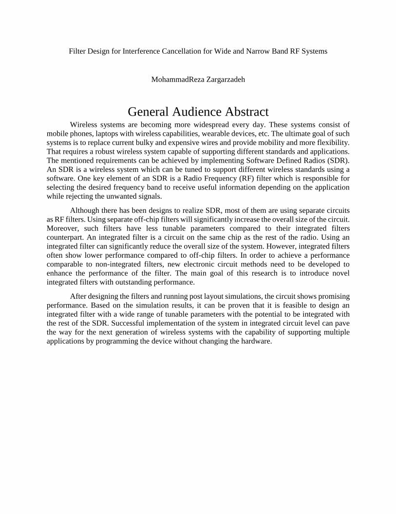
Filters are also needed in transmitters. Figure 2.2 shows a Heterodyne transmitter where a
band pass filter (BPF) is used after the second stage mixer. As can be observed from the figure,
the filter is proceeded by a power amplifier (PA) which is responsible for delivering the required
power to the antenna. The required power is usually set by the standard. If the output power of the
PA is large (for example 30 dBm), the input power of it may also be considerable since PA is only
5
capable of providing a limited gain. In this case, linearity of the filter plays a crucial role in the
transmitter chain. While the noise figure on the transmitter side is not a major concern, it has to be
kept below the maximum out of band level allowed by the standard.
Antenna
PABPF
Mixer 2
Mixer I1
Mixer Q1
I
Q
Figure 2.2 Heterodyne transmitter architecture
In a two-way communication, devices are designed to accomplish both receiving and
transmitting. In this case, if the transmitter (TX) and receiver (RX) send and receive at the same
time using the same frequency band, interference occurs and information loss takes place.
Consequently, methods called multiple access techniques are compulsory to make the
simultaneous transmit and receive feasible. There are three well-known multiple access
techniques. Time Division Multiple Access (TDMA) is a method where the same frequency band
is utilized by TX and RX concurrently. In order to avoid interference in this method, time slots are
assigned to each path where TX and RX are only active in their own allowed time. In TDD
transceivers, a switch is often used between TX and RX to avoid leakage. Code Division Multiple
Access (CDMA) is another method of multiple access which utilizes orthogonal codes for each
path in order to facilitate information transfer from different paths at the same time. Finally,
Frequency Division Multiple Access (FDMA) allocates different frequency spectrum to TX and
RX to avoid interference. FDMA makes it possible for the transceiver to transmit and receive at
the same time. However, due to the non-idealities of RF blocks, a portion of transmitted signal
may leak into the receiving path. This is demonstrated in Figure 2.3. This type of leakage is called
self-interference or in-band interference, and it can be avoided by placing a filter called duplexer
between TX, RX and antenna. The role of the duplexer is to allow passing of the signal from
antenna to RX and from TX to antenna while blocking any signal passage from TX to RX. [3]

6
RX
TX
To
Baseband
From
Baseband
Antenna
Duplexer
Figure 2.3 A transceiver with duplexer supporting FDMA
2.1.2. Performance Metrics Filters are categorized in five types of low pass (LPF), high pass (HPF), band pass (BPF),
band stop or notch (BSF) and all pass (APF). In this research, the focus is on BPF and BSF. The
first important metric for a BPF or BSF is the center frequency. When the center frequency of a
filter is determined, it is important to gain information on how wide the pass-band is and how sharp
the transition from band pass to band stop would be. The former is determined by 3-dB bandwidth
in a BPF, and the latter is characterized by the order of the filter. For BSF, the two mentioned
parameters are determined by its BPF counterpart which will be explained later in this section. A
BPF (or BSF) can be as low as second order and the general transfer function for a second order
BPF, which is what this research is mostly concentrated on, is as follows:
H(S) = Av
ω0Q
S
S2+ ω0Q
S+ ω02 (2.1.1)
Where Av is the pass band gain, ω0 is the center frequency and Q is the quality factor which is
proportional to the ratio of the center frequency divided by the bandwidth of the filter. The transfer
function of a BSF is derived by subtracting a constant equal to the gain of the BPF from its transfer
function. The transfer function of a second order BSF will then be:
H(S) = AvS2+ ω0
2
S2+ ω0Q
S+ ω02 (2.1.2)
The general form of BPF and BSF frequency response is shown in Figure 2.4. As can be observed
from the figure, all three mentioned parameters of BPF can be determined from its frequency
response. However, bandwidth (or Q) cannot be measured directly from the frequency response of
BSF. In order to measure Q for a BSF, an all pass response has to be subtracted from it.

7
Frequency
Gain
3-dB
Frequency
Gain
Figure 2.4 band pass filter (left) and band stop filter (right) frequency response and their
performance characteristics
At the presence of a blocker, it is important to adjust the center frequency of the band pass
filter and its bandwidth to select the desired band while rejecting the interferer. If the blocker level
is large, a band stop filter is used and its center frequency is placed in the frequency of the blocker
and its bandwidth is adjusted according to the blocker’s bandwidth. Therefore, the range of Q and
center frequency tunability are important performance metrics.
The metrics introduced in the previous paragraph are all linear metrics neglecting the
nonlinear effects. The assumption is valid if the filter used is a passive filter with no active
component. However, in order to make the filter frequency and Q tunable, nonlinear components
may be added to the system. Therefore, nonlinearity has to be quantified. There are two types of
nonlinearity in filters, out of band nonlinearity, which determines how blocker resilient the system
is and in band linearity defined to measure the linearity of the system when processing the desired
signal. Both in band and out of band linearity can be defined in terms of 1-dB compression point
or 3rd order intercept point (IP3). For 1-dB compression point, the input power is increased until
the gain is dropped by 1-dB. Depending on the frequency of the tone, it defines in or out of band
linearity. For IP3, two tones (in or out of band) are applied to the system and by applying the
following formula, IP3 can be obtained:
IP3 = P(main tone) + ∆P
2 (2.1.3)
Where ∆P is the power difference between the main tones and their third order products. This
method is called two tone test. 1-dB compression point and 3rd order intercept points are
demonstrated in Figure 2.5.

8
Input Power
Gain
1-dB
Frequency
Power
Input 1-dB
Compression
Main tones
∆
Figure 2.5 1dB-Compression point (left) and two tone test (right) for third order intercept point
calculation
When multiple stages are cascaded, the overall third order intercept point (or 1-dB
compression point) in term of IP3 of each stage can be approximated as:
1
AIP3,total2 =
1
AIP3,12 +
α12
AIP3,22 +
α12α2
2
AIP3,32 + ⋯ (2.1.4)
Where αi is the linear gain of each stage. It can be concluded from 2.1.4 that the linearity of the
last stages is more important than the linearity of the first stages and as the gain of a stage increases,
it imposes stricter requirements for the linearity of its proceeding stage. This can also be implied
by intuition. In a receiver, the first stage experiences a low intensity signal and hence remains in
its linear region. However, if it amplifies the signal with a large gain, the second stage may not
necessarily work only in its linear region around its bias point. In conclusion, if the target filter is
a duplexer or a band select filter appearing before the LNA the linearity is not of main concern.
However, for the channel select/image reject filters the effect of nonlinearity becomes more severe.
It is important to mention the relaxed linearity requirement for the first stage filters may not always
be true. While the signal level at the first stage is low in most cases, the interference level may not
be. Therefore, high out of band linearity may be required while low in band linearity could be
sufficient. Another important fact is that although the issue of out of band interference is not of
concern on the transmitter side, self-interference due to the nonlinear elements in a transmitter
could be detrimental to the receiver.
Noise is another issue which needs to be addressed in RF filter design since it determines
the sensitivity and the dynamic range of the receiver. Sensitivity is defined as the minimum
detectable signal with an acceptable quality and is calculated by the following formula:
Psensitivity = 174dBm
Hz+ NF + 10log(Bandwidth) + SNRmin
(2.1.5)
Where NF is the overall noise figure of the system and SNRmin is the acceptable signal to noise
ratio. The overall noise figure of the system is obtained using Friis equation:
NFtot = NF1 + NF2−1
AP1+ ⋯+
NFm−1
AP1…AP(m−1) (2.1.6)
9
Where AP is the power gain of each stage and m is the number of stages. If the gain of the first
stage is large, the overall noise figure is determined by the noise figure of the first stage and the
noise figure of the following stages will be negligible. Therefore, if a filter is not on the first stage
of a receiver, its noise figure requirement will be more relaxed.
As it will be explained in next chapter, a trade-off exists between NF and linearity.
Consequently, one can improve NF by degrading linearity and vice versa. However, this type of
improvement is not considered as an improvement in the system. In order to have a fair comparison
between different filter structures, dynamic range is defined as the maximum input level a receiver
can handle divided by the minimum level it can process. Therefore, even if NF is improved at the
cost of linearity the dynamic range remains constant. There are different standards for the
maximum power a system can handle. For this research, the focus is on linear dynamic range which
is defined by:
DRl = P1−dB Psenstivity (2.1.7)
Where P1−dB is the 1-dB compression point and Psensitivity can be obtained from equation 2.1.5.
[3]
2.2 Filter Topologies Filtering is a general mathematical concept independent of its actual implementation.
While mathematically, there is a singular way to define a second order band pass filter, the filter
implementation could be in multiple methods. In this work, the focus will only be on analog and
mixed-signal filters where the implementation is accomplished in electronic circuit level design.
The concept of analog filtering is an old concept dating back to 1915. However, the monolithic
filters became widespread after 1980. Using Integrated Filters for RF communication was
introduced after 1996 when active RLC prototypes were implemented [6]. Integrated filtering for
interference cancellation is an ongoing hot topic thanks to the invention of software defined radios
(SDR) where filter tuning using software becomes attractive.
Over the past decades, with the development of Integrated Circuit technology, high quality
active and passive components were realized which caused different filter topologies to emerge.
In this section, different filter topologies will be studied and their pros and cons will be
qualitatively discussed and the detailed quantitative comparison of the best achieved performances
will be left to section 2.3.
2.2.1. Passive Filters Passive filters in traditional way are the most basic type of filters. However, the term
passive can be applied to all filters where active elements are not an integral part of filtering
function. In this section, two types of passive filters will be discussed. The first type, traditional
passive filters are the design targets of this work and additional circuitry will be added to them to
boost the performance. Since the added circuits will have active elements, these type of filters are
regarded as active Q-enhanced LC filters. However, they are different than other types of active
filters which will later be discussed in this chapter.
The second type, N-path filter is another emerging filter in the state of the art RF tunable
filter design.

10
Traditional passive filters consist of pure passive elements to synthesize the desired transfer
function. The first design step of most type of filters starts by designing a passive prototype
and converting it to the desired active topology in later steps. Therefore, understanding
passive filters is not only essential for the designing of passive filters themselves but also
it is imperative to design a non-passive filter. The most basic types of passive filters are
RC and RL filters. An RC filter is demonstrated in Figure 2.6. The input-output transfer
function for a first order RC filter can be obtained as: Vout(S)
Vin(S)= H(S) =
1
1+SRC (2.2.1)
2.2.1 is a low pass filter with a cut-off frequency of 1 2𝜋𝑅𝐶⁄ . The high pass counter part
of the mentioned filter can be synthesized by substituting R and C which leads to the high
pass function with the same cut-off frequency.
LPF HPF
Figure 2.6 First order low pass (left) and high pass (right) filters
Low pass and high pass functions can also be implemented using R and L. The in common
characteristic between all the mentioned filters is that they are one pole systems. In a one
pole system the energy delivered from the source can be stored in one element and if the
source is turned off the stored energy starts dissipating in the resistor until it vanishes. In
order to realize a band pass function, at least one RLC tank has to be used. When L and C
are placed together in a circuit, they can exchange energy between each other. In this case,
the system becomes a two pole system. It is important to mention a two pole system can
also be synthesized by cascading two one pole systems. However, that doesn’t produce a
band pass function. In an RLC circuit, the stored energy in L or C starts a decaying
oscillation when the source of the energy is nulled. As R increases, the oscillation continues
to run for a longer period. The frequency of the oscillation is 1 2π√LC⁄ . The mentioned
phenomena can be translated into the Quality factor (Q) of the band pass transfer function.
When R is larger, the filter is more selective around the frequency of oscillation and
consequently leads to a higher Q. The basic diagram of RLC circuits are shown in Figure
2.7. The left diagram is when the tank input is a voltage source and the right diagram is
when the input of the tank is current. Both circuits show same behavior and they are
Thevenin/Norton equivalent of each other.

11
Figure 2.7 Thevenin (left) and Norton (right) second order band pass filters
The transfer function of the Thevenin circuit is:
Vout(S)
Vin(S)= H(S) =
1
RCS
S2+ 1
RCS+
1
LC
(2.2.2)
And for the Norton circuit:
Vout(S)
Iin(S)= H(S) = R
1
RCS
S2+ 1
RCS+
1
LC
(2.2.3)
The difference between 2.2.2 and 2.2.3 is that the pass band gain for the voltage driven
circuit is 1 while it is proportional to the tank resistance for the current driven case. The
practical pros and cons of each circuit will be discussed in detail in chapter 3. By comparing
2.2.2 with 2.1.1, Q can be derived as R (√L C⁄ )⁄ and by dividing the center frequency by
Q, the bandwidth of the filter will be 1 RC⁄ . In circuits of Figure 2.7, the center frequency
of the tank can be controlled by changing the capacitance (or the inductance) and the band
width (Q) of the circuit can be fully controlled by changing the resistance. However, this
is only valid when the Q of the capacitor and inductor are infinite. When the storing
elements (L and C) have finite Q, the Q of the tank is limited by the Q of the elements.
Figure 2.8 shows how finite Q of the elements impact the equivalent resistance of the tank
and consequently degrade the bandwidth of the circuit.
Figure 2.8 The effect of finite Q of the elements on the overall Q of the system
Where RL and RC are (Lω0) QL⁄ and 1 (QCCω0)⁄ respectively and QL and QC are the Q
of each component which depends on the technology used to fabricated them. By applying
series to parallel conversion at the center frequency of the tank, RL and RC
are derived as
(1 + QL2). RL and (1 + QC
2). RC. By assuming the Q of the components are large
enough, L and C remain unchanged after series to parallel conversion. After the conversion,
the new Q of the system will be Req (√L C⁄ )⁄ where Req = R||RL ||RC
. In practice,
capacitors have higher Q and the equivalent resistance of the tank will be the parallel of

12
tank resistance and inductor resistance. While R can be implemented as a variable resistor
by using CMOS transistors, the designer doesn’t have much control over the value of RL.
Therefore, the Q tuning using R will only be limited to the cases where the tank resistance
is significantly smaller than parallel inductor resistance. That limits the maximum
achievable Q to less than 15 in 4 to 8 GHz frequency range using IBM 0.13 µm BiCMOS
technology. It can be concluded that if only passive components are used in a filter, a very
selective filter cannot be implemented. In order to address the issue of low Q, Q-
enhancement techniques are used to boost the Q to higher values. While the
implementation of the Q-enhancement circuits varies, the basic of all of them is to design
a negative resistance circuit which can cancel out the finite resistance of the elements. Since
negative resistance is achieved by using active components, Q-enhanced filters are
regarded as active filters.
A band-stop filter has also been designed in this thesis. The circuit diagram of a band stop
filter is demonstrated in Figure 2.9. Similar to its band pass counterpart, a band stop filter
can be inputted with both voltage and current.
Figure 2.9 Thevenin (left) and Norton (right) second order band stop filters
The transfer function for the Thevenin circuit is:
Vout(S)
Vin(S)= H(S) =
S2+ 1
LC
S2+ R
LS+
1
LC
(2.2.4)
And for the Norton’s equivalent:
Vout(S)
Iin(S)= H(S) = R
S2+ 1
LC
S2+ R
LS+
1
LC
(2.2.5)
Comparing both of the equation with 2.1.2, the center frequency of the filter will be 1 √LC⁄
with the Q of (√L C⁄ ) R⁄ . For the voltage-driven circuit, the gain is unity while it is
proportional to the resistance for the current-driven one. In a band stop filter, in contrast to
band pass filter, the Q is inversely proportional to the resistance of the circuit. While this
may not be important in theory, it introduces serious practical issues for the implementation
of a band stop filter. For the proposed design, as it will be explained in next chapters, the

13
characteristic impedance of the tank which can be calculated from √L C⁄ is in the order of
10. As an example, if the value of the resistance is in the order of 1 Ω, the Q of the circuit
limits to the values less than 10. When laying out a circuit, the parasitic resistance of 100
mΩ and larger is typical. Even if the resistance is reduced by using thicker lines, the circuit
still needs a driver. For the voltage driven case, the typical value of the driver’s resistance
is tens of ohms. For current driven circuit, although driving with a very small resistance
might be possible, the gain is also proportional to the resistance meaning the gain has to be
compromised to achieve a large Q. If the circuit is designed to provide a 100 mΩ resistance,
a transconductance of at least 10 A V⁄ is required to keep the gain at 0 dB. This value is
impractical in BJT and CMOS circuits. Reducing the transconductance to any value less
than 10 A V⁄ makes the filter a lossy element and consequently the NF gets degraded.
Therefore, using only passive elements, it is not possible to achieve a high Q band stop
response. It will be explained in next chapters how the mentioned issue is going to be
addressed.
The invention of N-path filter which is another type of passive filters dates back to 1960.
N-path filter is an alternative approach to the traditional passive filters in order to realize
filter transfer functions [7]. The basic idea of N-path filter is conceptually demonstrated in
Figure 2.10 [4]:
p
p
p −
q
q
q −
Figure 2.10 Block diagram of an N-path filter architecture
In the figure, p(t) and q(t) are mixing functions aiming to up and down convert the signal,
T is the period of the mixing function and h(t) can be any arbitrary function depending on
the desired functionality of the system. The detailed analysis of N-path filters is beyond
the scope of this work. However, in order to compare the performance, a band pass filter
architecture is explained. A band pass N-path filter operation is shown in Figure 2.11. In
order for the system to act as a band pass filter, h(t) needs to be a low pass function. The

14
circuit down converts the signal to base band using p mixers. In baseband, a sharp low pass
function is implemented. After up conversion with q functions, the output is a band pass
filter with the center frequency equal to the frequency of mixing functions and the
bandwidth equal to the cut-off frequency of low pass h(t).
Frequency
Gain
Frequency
Gain
Frequency
Gain
∆
∆
Figure 2.11 Conceptual N-path frequency plots for a band pass filter
While each block in the filter can be implemented in different ways, the design presented
in [4] is the basic of all current N-path filter designs. The circuit schematic of a band pass
filter using N-path technique along with its simplified version is shown in Figure 2.12. The
low pass function is implemented using an RC circuit. Passive switches are used to realize
mixing functions. Since both p and q mixers are in phase for each path, the circuit sees an
RC when both are on and an open circuit when both are off. Therefore, they can be replaced
by one switch in order to simplify the circuit. Non-overlapping clocks have to be generated
for each path. As can be observed from the figure, all the elements used in an N-path filter
are passive elements. Therefore, N-path filters can be regarded as passive filters. However,
there are different from traditional passive filter in the sense that mixing function is used
in them which is a nonlinear function in order to realize a band pass filter while traditional
passive filters only use linear elements. N-path filters are capable of providing an
outstanding linearity due to the using of only linear elements and passive mixers. The
power consumed by the circuit is only coming from the clock generation part and it
increases as the frequency of operation increases. This fact makes N-path filters less
desirable at higher frequency ranges. Moreover, generating non overlapping clocks can be
extremely challenging at high frequencies. Another factor limiting the performance of N-
path filters is the resistance and parasitic capacitance of the switches. It can be shown the
mentioned non idealities of switch degrades selectivity of the filter.
15
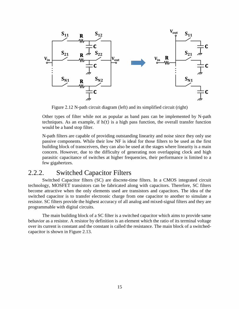
Figure 2.12 N-path circuit diagram (left) and its simplified circuit (right)
Other types of filter while not as popular as band pass can be implemented by N-path
techniques. As an example, if h(t) is a high pass function, the overall transfer function
would be a band stop filter.
N-path filters are capable of providing outstanding linearity and noise since they only use
passive components. While their low NF is ideal for those filters to be used as the first
building block of transceivers, they can also be used at the stages where linearity is a main
concern. However, due to the difficulty of generating non overlapping clock and high
parasitic capacitance of switches at higher frequencies, their performance is limited to a
few gigahertzes.
2.2.2. Switched Capacitor Filters Switched Capacitor filters (SC) are discrete-time filters. In a CMOS integrated circuit
technology, MOSFET transistors can be fabricated along with capacitors. Therefore, SC filters
become attractive when the only elements used are transistors and capacitors. The idea of the
switched capacitor is to transfer electronic charge from one capacitor to another to simulate a
resistor. SC filters provide the highest accuracy of all analog and mixed-signal filters and they are
programmable with digital circuits.
The main building block of a SC filter is a switched capacitor which aims to provide same
behavior as a resistor. A resistor by definition is an element which the ratio of its terminal voltage
over its current is constant and the constant is called the resistance. The main block of a switched-
capacitor is shown in Figure 2.13.
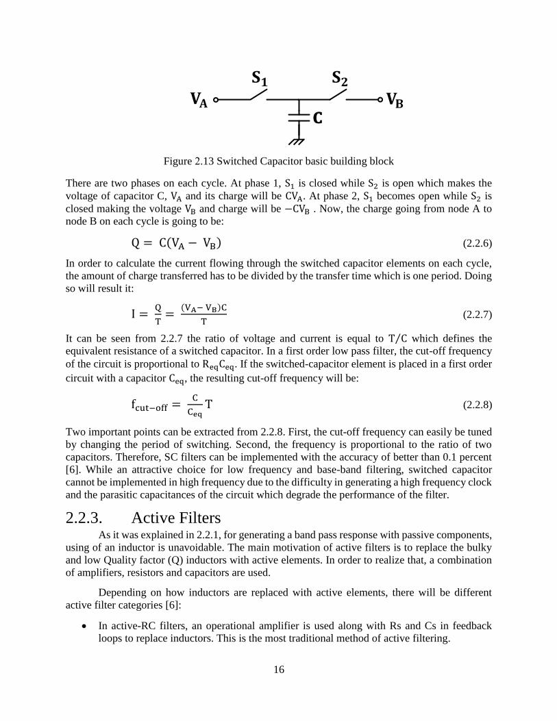
16
Figure 2.13 Switched Capacitor basic building block
There are two phases on each cycle. At phase 1, S1 is closed while S2 is open which makes the
voltage of capacitor C, VA and its charge will be CVA. At phase 2, S1 becomes open while S2 is
closed making the voltage VB and charge will be CVB . Now, the charge going from node A to
node B on each cycle is going to be:
Q = C(VA VB) (2.2.6)
In order to calculate the current flowing through the switched capacitor elements on each cycle,
the amount of charge transferred has to be divided by the transfer time which is one period. Doing
so will result it:
I = Q
T=
(VA− VB)C
T (2.2.7)
It can be seen from 2.2.7 the ratio of voltage and current is equal to T C⁄ which defines the
equivalent resistance of a switched capacitor. In a first order low pass filter, the cut-off frequency
of the circuit is proportional to ReqCeq. If the switched-capacitor element is placed in a first order
circuit with a capacitor Ceq, the resulting cut-off frequency will be:
fcut−off = C
CeqT (2.2.8)
Two important points can be extracted from 2.2.8. First, the cut-off frequency can easily be tuned
by changing the period of switching. Second, the frequency is proportional to the ratio of two
capacitors. Therefore, SC filters can be implemented with the accuracy of better than 0.1 percent
[6]. While an attractive choice for low frequency and base-band filtering, switched capacitor
cannot be implemented in high frequency due to the difficulty in generating a high frequency clock
and the parasitic capacitances of the circuit which degrade the performance of the filter.
2.2.3. Active Filters As it was explained in 2.2.1, for generating a band pass response with passive components,
using of an inductor is unavoidable. The main motivation of active filters is to replace the bulky
and low Quality factor (Q) inductors with active elements. In order to realize that, a combination
of amplifiers, resistors and capacitors are used.
Depending on how inductors are replaced with active elements, there will be different
active filter categories [6]:
In active-RC filters, an operational amplifier is used along with Rs and Cs in feedback
loops to replace inductors. This is the most traditional method of active filtering.

17
In some cases, the technology available to the designer is not capable of providing high
quality resistors. In those cases, the resistor can be replaced by a MOSFET transistor where
the new category is called MOSFET-C filters. Although MOSFET-C structure makes the
integration of the filter using traditional technologies possible, it comes with drawbacks.
MOSFET transistor is an active element in contrast to a simple resistor where voltage and
current relation is always linear. This introduces nonlinearities compared to the original
active-RC filter. In addition to the previous disadvantage, every MOSFET transistor
requires a certain gate to source voltage to realize a certain value of resistance. If that
voltage changes, the resistor will change. Therefore, the voltage swing will be limited in
MOSFET-C filter compared to active-RC.
Gm-C or OTA-C is another category of active filters. In contrast to the active filters
introduced so far where feedback loops are employed, Gm-C filters are open loop filters.
This makes Gm-C filters a more attractive solution compared to other types of active filters
for high frequency applications. Another advantage of this filter is unlike MOSFET-C, the
tuning and swing can be independent of each other. It will be explained in 2.3 that while
Gm-C filters are attractive for frequencies up to 1 GHz. Q-enhanced filter is still superior
for higher frequencies due to its higher dynamic range for the same Q.
In the design of each active filter, first, the type and order of the filter is determined based
on the design requirements. Second step is the passive realization of selected filter using Rs, Ls
and Cs. After this step, inductors are transformed to active elements depending on the type of
active filter to be used in the design.
Active filters are attractive solutions where high performance is needed in a moderate
frequency and the silicon area is limited. However, they suffer from lower accuracy compared to
switched capacitor filters. Therefore, a tuning circuitry is often used to reach an accuracy of better
than 1 percent. Another shortcoming which makes it impractical to design an active filter for this
research is lack of a practical method for Q tuning which is one of the design requirements of this
work.
2.3 Literature Review While one of the limitations of active-RC filters is the fact they are based on feedback
techniques, with the advent of new advanced technologies, their implementation in higher
frequencies becomes more feasible. [8] presents an active-RC filter for 0.8 to 2.2 GHz frequency
range. Due to the high NF of around 20 dB, the filter has to be used after an amplifier which can
be done since circuit shows outstanding in and out of band IIP3. While the active filter presented
in this paper achieves a promising performance, there is still lack of Q tuning technique for the
filter. Although there has been numerous effort to improve the performance of active-RC filters
for RF applications, the maximum operating frequency hasn’t been exceeded to more than 3 GHz
to the knowledge of the author.
The major focus of recent RF filter designs has been on N-path filters. As mentioned in the
previous section, the concept of N-path filtering is an old concept. However, [4] has revolutionized
the use and modeling of N-path filters for RF frequencies with tuning capabilities. There have been
efforts since then to implement different types of filters using the N-path technique. [9] presents
6th order filter using the N-path technique for 600 MHz to 850 MHz. The design provides an in-
band 1-dB compression point of 0 dBm with the NF of 8.6 dB. Q ranges from 40-90 along the

18
frequency range and it is not tunable. [10] develops a new filtering structure by combining the N-
path filter with gm-C resulting a 4th order band pass filter with the frequency ranging from 0.4 to
1.2 GHz. The filter has the in-band 1-dB compression point of -4.4 dBm and NF of 10 dB. The
bandwidth of the filter is 21 MHz and it is not tunable. [11] presents a 6th order band pass filter for
0.1 to 1.2 GHz frequency range with the NF of 2.8 dB and bandwidth of 8 MHz. There is no data
on the in-band linearity of the filter. However, the filter is capable of tolerating up to +7 dBm of
blockers.
Q-enhanced LC filters have also been developed for RF applications. In [12], a Q-enhanced
LC filter has been designed for 1.98 to 2.02 GHz frequency range with the NF of 15 dB and in-
band 1-dB compression point of -6.6 dBm. The filter provides 130 MHz of bandwidth for 2 GHz
center frequency and it is not bandwidth tunable. Although employing Q-enhanced LC structures
in the TRX chain is common, designing RF filters using the technique has not been a major focus
for RF designers. Recently, [5] has proposed a Q-enhanced 2nd order LC band pass filter capable
of both frequency and bandwidth tuning. The frequency operation of the circuit ranges from 2.25
to 4.5 GHz. Q is tunable from 5 to 150. NF ranges from 10 dB for the minimum Q and rises up to
18.5 dB for the highest achieved Q. 1-dB compression point is ranging from -8 dBm to 9 dBm. A
4th order version of [5] has been implemented in [13]
The second design in this work is a band stop filter (notch). Therefore, recent works on
notch has to be studied as well. The mentioned techniques for band stop filter can also be used to
create a notch. In [14], efforts have been done to design and model notch filters using N-path
concept. A tunable notch with the center frequency ranging from 0.1 to 1.2 GHz has been designed.
The notch is capable of providing up to 24 dB of rejection while imposing 1.6 dB to 2.5 dB of NF
with the 1-dB compression point of better than 2 dBm. No Q tenability has been reported for this
design.
[15] develops LC notch along with a low noise amplifier capable of achieving up to 35 dB
of rejection along its frequency range of 5 to 6 GHz. With the noise figure of better than 6.2 dB
the in band 1-dB compression point of the filter is better than -30 dBm.
Notch filter has also been developed using RF MEMS. [16] demonstrates a high
performance notch with 40 dB of rejection along 1.1 to 2.7 GHz frequency range with the
bandwidth of 125 MHz. Although the notch presented in the mentioned paper shows high
performance characteristics, it cannot be compared with CMOS and BiCMOS Integrated Circuits
since it is not capable of software based tuning.
[17] implements a band stop filter by subtracting a Q-enhanced filter response from an all
pass response. Two filters are designed for 2 to 4 GHz and 4 to 8 GHz ranges. The 2-4 GHz
prototype can provide as high as 50 dB rejection with the NF of 12.8 to 13.5 dB and 1-dB
compression point of -3 dBm to -1 dBm. For 4 to 8 GHz design, the numbers are 8 to 10.8 dB of
NF and -9 to -6 dBm of 1-dB compression point.
The designs mentioned so far are listed as band stop and band pass filters. There are other
systems called “interference cancelling” systems which are aimed to provide same functionality
of the mentioned filters by employing additional circuit techniques compared to traditional filters.
[18] categorizes the interference cancelling techniques into three categories of frequency
translational filtering, feedback filtering and feedforward filtering. The three mentioned techniques
are demonstrated in Figure 2.14.

19
RF
LO
LPF
BB BB
BSF
LNA
RF BB
BSF
LNA
RF
Figure 2.14 Interference Cancellation Techniques – Frequency translational filtering (left),
Feedforward filtering (middle) and Feedback technique (right)
Frequency translational technique is a technique where the signal is down-converted to the
low frequency and low pass-filtered to mitigate the blocker. It is more trivial to perform filtering
function in base band than RF. If the mixer used before the filter is a passive mixer, the system
will be highly linear at the cost of high NF. The technique can also be used to reject the leakage
from the transmitter to receiver. However, the noise imposed by transmitter to receiver has to be
carefully studied. In addition to all the mentioned characteristics, this structure has the pros and
cons of direct conversion receivers such as flicker noise and LO feedthrough to antenna.
Feedforward is a method where the signal is rejected in an alternative path and is then
subtracted from the main path in order to cancel the interferer. The notch in the alternative path
can be implemented using different methods. [19] proposes a new design based on the feedforward
technique. The notch is implemented in the paper using down-conversion and high pass filtering
followed by an up-conversion. While the architecture can show a promising performance, the noise
imposed by the alternative path has to be reduced. Moreover, since the interferer is not mitigated
at the input, the low noise amplifier (LNA) has to be able to handle large blockers without going
to saturation.
The third technique is called feed-back. Both of the designs in this work are based on this
method. In the feedback method, the notch is placed in the feedback path and by applying gain to
feedback, the out of band signal level is reduced while the level of in band signal remains
unchanged and consequently the system can provide large Q and high out of band rejection. The
advantage of the feedback system proposed in 2.14 is the blocker is cancelled before the LNA and
hence the linearity requirement of the amplifier will be more relaxed. In this method, the stability
of the circuit has to carefully considered since all feedback systems have the potential to become
unstable. Moreover, the noise penalty by the feedback path increases if a high rejection is desired.
This will be explained in the implementation of the system in next chapter. Same as feedforward
system, the implementation of the notch can vary. The notch can be synthesized by placing a band
pass filter in the main path and subtracting it from an all pass response as the filter implemented
in [17]. The output of the notch can then be fed back using a variable gain amplifier to control the
Q of the system.
2.4 Chapter Summary This chapter starts by introducing the basic concepts of RF filtering and its importance in
both transmit and receive chain. Then, the important parameters and performance characteristics
are introduced. After introducing the basics of filtering, three different types of passive, switched
capacitor (mixed-signal) and active filters are discussed. For each type of filter, the basics are
discussed and the advantages and disadvantages of each type of filter are reviewed. Lastly, the

20
most recent work on each type of filter is presented. Moreover, the concept of interference
cancelling and its different types of frequency translational, feed forward and feedback is
discussed. For each mentioned method, the pros and cons are mentioned. The proposed design in
this work will consist of Q-enhanced LC filter design as well as employing feedback based
interference cancelling technique to achieve a better performance.

21
3 Chapter
Proposed Designs There are two proposed designs for this work. Both of the systems are required to have a
wide center frequency and bandwidth tuning range. The most important requirement for an
interference canceller is to be able to tolerate strong interferers without going into nonlinear region.
Noise is another important factor that needs to be considered especially if the systems are meant
to be used in the receiving chain. High linearity and acceptable noise figure along with wide
bandwidth and center frequency tuning range is achieved by adding a feedback path to Q-enhanced
LC filters.
This chapter starts by defining the design requirements for the band pass and band stop
filters. Then, the block diagram of the proposed solutions will be introduced to gain a better
understanding of the techniques employed for this work. The circuit details of each design will
then be explained by mentioning component values. In order to model the nonlinearity of the LC
tank for the designs of this work, the Volterra nonlinearity analysis of the varactors along with
simulations verifying the analysis will be presented. A nonlinear feedback-based model of the LC
tank will also be introduced and compared with Volterra analysis.
3.1 Design Requirements The proposed BPF is an enhancement based on the system designed by Laya Mohammadi
[5]. While mentioned system is a second order Q-enhance LC filter designed for 2-4 GHz
frequency range, the target of this thesis is to design a BPF for 4-8 GHz with the Q ranging from
lower than 10 up to 150 and more. Q tuning is attractive since the position of the blocker in
frequency spectrum varies and higher Q may be required if the blocker is closer to the desired
signal.
In a Q-enhanced filter, the noise increases as Q increases [5]. Moreover, since a nonlinear
element is used to increase the Q of the filter, 1-dB compression point (in band) is increased for
the higher Q cases. As it has been shown in [5], 1-dB compression point can be as high 10dBm for
low Q and -10dBm for high Q. Minimum NF varies from 10 dB for low Q and 20 dB for the Q of
higher than 100.
The notch is designed for 4 - 8 GHz frequency range as well. The design is based on 0.13
µm BiCMOS where fT of CMOS transistors are limited to less than 100 GHz while HBT transistors
are capable of providing up to 200 GHz. However, if a more advanced CMOS technology is used,
the same idea can be implemented for higher frequency ranges. The minimum depth of the notch
is targeted to be at 40 dB. However, it should be adjustable for the cases where 40 dB is not
required. NF has to be lower than 8 to 10.8 dB, which is reported at [17], and 1-dB compression
point should be better than -6 dBm to -9 dBm, which is reported at [17]. Moreover, depending on
the bandwidth of the blocker, Q has to be tuned from values below 10 to 60 and higher.

22
As it will be explained later in this chapter, both of the systems proposed in this research
are feedback based where stability is a major issue. Therefore, K stability factor has to be simulated
and kept above 1 in order to ensure proper function of the systems.
3.2 Block Diagram
3.2.1. Band-Pass Filter The basic idea of this design originates from the notch proposed in [17]. In a negative feedback
system with the forward gain of AOL and loop gain of T, the input-output relationship is:
OUT = IN AOL
1+T (3.2.1)
Comparing it with an open-loop system where the input is only multiplied by AOL, it can be
concluded that the signal gets smaller by the factor of 1 (1 + T)⁄ in a feedback system compared
to an open-loop system if a circuit can be designed in a way that only out of band signals appear
in the feedback path, their magnitude can be reduced by increasing the loop gain. One method to
achieve the mentioned goal is to synthesize a notch using a Q-enhanced band-pass filter and an
all-pass filter and obtain the notch by subtracting the output of the two filter. The synthesized notch
then can be fed back to the input with a variable gain amplifier which controls the loop gain. The
mentioned system is shown in Figure 3.1.
BPF
APF
Frequency
Gain
Frequency
Gain
Figure 3.1 Synthesized notch based feedback interference cancelling system
As depicted, the notch is synthesized at the node Vnotch and is fed back using the gain block of AV.
If all the blocks used in Figure 3.1 are ideal, by increasing the loop gain, the out of band signal
will be rejected while the in band signal will remain unchanged. Using this method, the Q of the
filter can be adjusted to the desired value. Q-enhancement can also be proved mathematically. If
the transfer function of the band pass filter is assumed to be:

23
H(S) =
ω0Q
S
S2+ ω0Q
S+ ω02 (3.2.2)
Then the overall transfer function of the closed loop system of Figure 3.1 can be obtained as:
H(S) =
ω0Q(1+ AV)
S
S2+ ω0
Q(1+ AV)S+ ω0
2 (3.2.3)
By comparing 3.2.2 with 3.2.3, it can be concluded that the Q of the new filter has been scaled by
1 + AV without changing the pass band gain.
There are three main issues with the design mentioned in Figure 3.1. First, the gain of band
pass and all pass filter should be perfectly matched. If any mismatch occurs, there will be interferer
as well as signal in the feedback path. This will not only degrade the performance of filter in terms
of Q but it also degrades the linearity of the system. This happens due to the fact that the band pass
filter could experience a positive feedback if any gain mismatch occurs between all pass and band
pass filters. Second, in the actual implementation of the filter, each node in the feedback path has
its own parasitic capacitance. This can potentially lead the system to an unstable state since each
pole degrades the phase margin of the system if it gets close to the operating frequency of the
circuit. Third, as mentioned, in order to get higher Q, the loop gain of the filter has to be increased.
This leads to an increase in the input-referred noise proportional to feedback. Therefore, with
increasing the Q, the noise figure of the system degrades dramatically which also can be proven
mathematically. If the output noise of the band pass filter is modelled as vn,BPF2 , the input referred
noise of the system due to the band pass filter noise is going to be:
vn,BPF,in2 = |(1 + AV)
S2+ ω0Q
S+ ω02
ω0Q
S|
2
vn,BPF,in2 (3.2.4)
Since only the in-band noise is important, it can be concluded the input referred noise due to the
band bass filter is increased by 1 + AV factor. Moreover, the output noise of the variable gain
amplifier directly appears at the input and it increases as its gain increases.
The short comings introduced make the system of Figure 3.1 not practical for high Q
especially due to its noise behavior. The main source of the problem is the synthesized notch is
not capable of completely decouple the band pass signal and its noise from the feedback path. A
solution proposed to that problem is to use an LC notch instead of a synthesized one. The proposed
solution is demonstrated in Figure 3.2.

24
BPF
Frequency
Gain
Frequency
Gain
BSF
Figure 3.2 Interference cancelling system based on an LC notch
For this system, the in band output noise of the band pass filter is suppressed by the notch.
Moreover, if the depth of the notch is enough, there will be no signal in the feedback path and
positive feedback does not occur. Therefore, the linearity does not get degraded. The system
proposed in 3.2 still cannot reduce the noise effect caused by the amplifier in the feedback. In order
to solve this issue, it is preferable to add the gain stage before the notch so that its noise gets
cancelled. Therefore, a modified version of the system proposed in Figure 3.2 is introduced in
Figure 3.3.
BPF
Frequency
Gain
Frequency
Gain
BSF
1
Buffer
Figure 3.3 Proposed system of this thesis based on feedback cancellation technique
In the system proposed in Figure 3.3, the only important noise is the noise of the buffer which has
to be minimized. The use of buffer is unavoidable since the output of the notch cannot be directly
fed to the band pass filter. Another advantage of the system is that the output parasitic capacitance
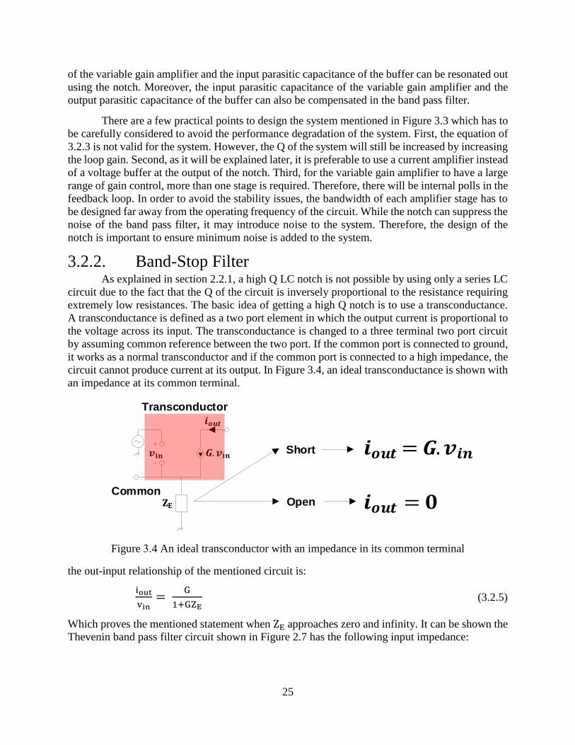
25
of the variable gain amplifier and the input parasitic capacitance of the buffer can be resonated out
using the notch. Moreover, the input parasitic capacitance of the variable gain amplifier and the
output parasitic capacitance of the buffer can also be compensated in the band pass filter.
There are a few practical points to design the system mentioned in Figure 3.3 which has to
be carefully considered to avoid the performance degradation of the system. First, the equation of
3.2.3 is not valid for the system. However, the Q of the system will still be increased by increasing
the loop gain. Second, as it will be explained later, it is preferable to use a current amplifier instead
of a voltage buffer at the output of the notch. Third, for the variable gain amplifier to have a large
range of gain control, more than one stage is required. Therefore, there will be internal polls in the
feedback loop. In order to avoid the stability issues, the bandwidth of each amplifier stage has to
be designed far away from the operating frequency of the circuit. While the notch can suppress the
noise of the band pass filter, it may introduce noise to the system. Therefore, the design of the
notch is important to ensure minimum noise is added to the system.
3.2.2. Band-Stop Filter As explained in section 2.2.1, a high Q LC notch is not possible by using only a series LC
circuit due to the fact that the Q of the circuit is inversely proportional to the resistance requiring
extremely low resistances. The basic idea of getting a high Q notch is to use a transconductance.
A transconductance is defined as a two port element in which the output current is proportional to
the voltage across its input. The transconductance is changed to a three terminal two port circuit
by assuming common reference between the two port. If the common port is connected to ground,
it works as a normal transconductor and if the common port is connected to a high impedance, the
circuit cannot produce current at its output. In Figure 3.4, an ideal transconductance is shown with
an impedance at its common terminal.
.
Common
Transconductor
Short
Open =
= .
Figure 3.4 An ideal transconductor with an impedance in its common terminal
the out-input relationship of the mentioned circuit is:
iout
vin=
G
1+GZE (3.2.5)
Which proves the mentioned statement when ZE approaches zero and infinity. It can be shown the
Thevenin band pass filter circuit shown in Figure 2.7 has the following input impedance:

26
Zin(S) = RS2+
1
RCS+
1
LC
S2+ 1
LC
(3.2.6)
The impedance of 3.2.6 approaches R at the frequency of zero and infinity and goes to infinity at
the center frequency of the tank, 1 √LC⁄ . Moreover, as RC gets larger, the transition from R to
infinity becomes more abrupt. It can be shown that if the tank is placed as ZE in Figure 3.4, a notch
can be formed at the output current. The proposed notch is demonstrated in Figure 3.5.
.
Common
Transconductor
+
+
+
Figure 3.5 Proposed notch
The output current in respect to the input voltage for the circuit of Figure 3.5 is:
iout
vin=
G
1+GR
S2+ 1
LC
S2+ G
1+GRCS+
1
LC
(3.2.7)
By assuming a large G and comparing 3.2.7 with 2.1.2, the out of band gain of the circuit is 1 R⁄
and the Q will be R (√L C⁄ )⁄ . As an example, if √L C⁄ which is the characteristic impedance of
the tank is 10, a resistance of 1 KΩ is needed to achieve the Q of 100. Using this amount of
resistance introduces two issues. First, a 1 KΩ resistance in an RF circuit can produce low
frequency poles to the system. Second, the out of band gain in this case is going to be 1 mmho
which requires a large resistance at the load to get larger than unity gain. Any load resistance
smaller than 1 KΩ causes the circuit to be lossy which degrades the noise figure of the system.
In order to enhance the behavior of the system, a feedback based notch is introduced. The
feedback is designed in a way it assists the circuit for large Q and it can be turned off for low Q to
avoid stability and noise issues. The basic idea of the feedback is the same as band pass filter. By
increasing the loop gain in the notch, the transition from its center frequency to pass band becomes
more abrupt. The block diagram of the feedback based notch is illustrated in Figure 3.6.

27
BSF
Frequency
Gain
Figure 3.6 Feedback assisted notch filter
The transfer function of the system of Figure 3.6 can be derived as:
Vout
vin=
1
1+AV
S2+ ω02
S2+ ω0
Q(1+ Av)S+ ω0
2 (3.2.8)
This equation states that the Q of the notch can be boosted by 1 + AV without having to change
the resistance of it. While the system in Figure 3.6 is capable of Q boosting, its gain is reduced by
1 (1 + AV)⁄ . This is not desirable since the gain of smaller than unity increases the noise figure
of the system. In order to address the issue, a Low Noise Amplifier (LNA) is added before the
system. This system which is implemented in this thesis is demonstrated in Figure 3.7.
BSF
LNA
Figure 3.7 Final version of the proposed feedback based notch consisting of a low noise
amplifier (LNA) to reduce the noise figure
One issue with adding an LNA is, while it reduces the noise figure, it degrades the overall linearity
of the system according to equation 2.1.4. However, since a feedback is used in this system, the
amount of linearity degradation is compensated by the loop gain.
It will be explained in section 3.3 that it is easier to add and subtract signal in the current
domain. Therefore, the subtraction in the system of Figure 3.7 is accomplished by subtracting the

28
output current of the LNA and variable gain amplifier. In consequence, the LNA and variable gain
amplifier will be transconductance amplifiers with a shared load. This causes noise degradation of
the system since LNA will not be able to suppress the noise imposed by the feedback path. In order
to avoid excessive noise by the feedback path, it should not be used with a large gain. As can be
concluded from the mentioned arguments, there exists a balance between the maximum Q obtained
from the open loop and its Q boosting by the feedback path in order to maximize the noise
performance.
It is also arguable that an adder in the voltage domain can solve the noise figure issue
caused by the feedback variable gain amplifier. However, adding more elements will add more
parasitic poles which is detrimental to a closed loop system in terms of stability. The design of the
LNA is another important issue since the amplifier has to be able to provide enough gain (around
20 dB) while keeping a low noise figure and high linearity to have minimum negative impact on
the overall system. As it will be discussed in section 3.3, since the circuit is implemented in the
differential configuration which makes the signals available in both positive and negative signs,
the subtracting block is embedded in the LNA and variable gain amplifier.
The block diagram of both of the systems designed in this work are explained in this
section. Both of the systems use feedback techniques with slightly different block diagrams. While
the implementation of the mentioned block diagrams may seem trivial, there are issues and
different methods to implement them. This will be fully discussed in the next section. The band
pass filter designed in this work operates in 4 to 8 GHz and is implemented using BiCMOS
technology. The notch is designed to work in 4 to 8 GHz and is implemented fully in CMOS.
3.3 Circuit Details In this section, the detailed schematic of each circuit will be discussed.
3.3.1. Band-Pass Filter The band pass filter is an improvement to the design proposed in [5] by adding extra
circuitry. A second order band pass filter is based on the schematic of Figure 2.7. In the integrated
circuit implementation, the Q of the inductor in 4 to 8 GHz frequency range is limited to less than
10. While by increasing R in Figure 2.7, the Q can be controlled, its maximum is limited to less
than 10 since all resistors need to be considered in determining the bandwidth. In order to
overcome the problem, a negative resistance has to be added in parallel with the LC tank to increase
the finite Q of the elements. A negative resistance can be as simple as a cross-coupled circuit.
However, a Darlington negative resistance is preferred to achieve larger negative resistance and
have better control resolution. The schematic of the Darlington negative resistance is demonstrated
in Figure 3.8.

29
Output
Figure 3.8 Darlington negative resistance
Based on the figure, there are two parts of fixed and variable resistances. The overall negative
resistance on each side assuming the current of each transistor is high can be calculated as
Rfixed||Rvar where Rvar can be varied to get the desired negative resistance depending on the
required Q.
Driving the LC tank is another important factor. The band pass filter of Figure 2.7 can be
voltage driven or current driven. When the circuit is voltage driven, the maximum achieved gain
is 1 while the gain of the circuit can be variable using the current driven circuit. A large gain in
the filter is important if a low noise figure is desired. This can be concluded from equation 2.1.6.
If the current driven circuit is going to be implemented, a common emitter can be used to create
the current. The current of the common emitter can be made variable by placing a variable
resistance at the emitter of the transistor. It can be verified that there is a trade-off between the gain
achieved by the transistor and its linearity. It is noteworthy to mention that the noise figure is not
always the main target of the design. If the interferer level at the input of the filter is large, the
circuit is required to have high linearity rather than a small noise figure. In this case, the voltage
driven band pass filter is used. The voltage driven circuit can be implemented by driving the
Thevenin equivalent of the tank with a common collector transistor. The common collector
configuration is capable of providing high linearity if it is biased at a fairly large current. The
circuit diagram of the band pass filter which is based on [5] is shown in Figure 3.9.

30
+ −
Figure 3.9 Q enhanced band pass filter using both voltage driven and current driven
configuration and Darlington negative gm cell to enhanced the Q
As seen from the figure, both voltage driven and current driven circuits are used and they can be
adjusted to compromise noise figure in order to get higher linearity.
In order to design the circuit working in 4 - 8 GHz range, the inductor value is designed to
be 650 pH differential meaning the circuit sees 325 pH on each side. The variable capacitor
(varactor) is designed in a way that its value can be varied between 1.23 pF and 4.2 pF. In the
design of the varactor, parasitic capacitance of the circuit has to be considered. The value of RQ is
set to change from very small value up to 350 Ω. While it is not considered in the schematic of
Figure 3.9, the circuit cannot provide 50 Ω matching at its input since the input of a BJT transistor
is a high impedance in this frequency range. In order to match the circuit for RF measurement, a
50 Ω resistance is placed between the base of input transistors and supply. This will significantly
degrade the noise figure of the system. However, it is necessary in order to perform RF
measurement. The size of the input transistors is also important in determining the noise figure of
the system. Although increasing the size of the transistors would introduce parasitic capacitance
at the input of the circuit which may degrade the performance, setting the size of them to the
minimum possible size will cause a large base resistance which is detrimental to the noise figure
of the system since it is on the first stage of the circuit.
If the finite resistance of the inductor and capacitor is fully compensated by the negative
resistance, the Q of the circuit can be determined by RQ √L C⁄⁄ . By plugging the design numbers
into the mentioned formula, the maximum Q achieved for this case ranges from 22 to 37. This is
clearly not enough for the design requirements of this work. Increasing the size of RQ to about four
times is not a practical solution. The only feasible solution is to increase the negative
transconductance further to increase the effective RQ. If the net negative resistance of the tank is
assumed to be Rtank, for the current driven path, the gain can be obtained by calculating the

31
parallel product of RQ and Rtank and multiplying that by the effective transconductance of the
transistor. For the voltage driven, the gain can be calculated as:
Vout
vin=
−Rtank
RQ−Rtank (3.3.1)
The magnitude of 3.3.1 can be greater than unity meaning the voltage driven path can potentially
provide gain in contrast to the case where the negative gm cell only cancels the tank resistance.
While having a gain of larger than one is usually desirable, for this case, it causes nonlinearity
since it is coming from the negative gm cell. Moreover, by increasing the strength of the negative
gm, the noise of the system increases significantly by causing both the noise current and the
effective resistance to rise. That is the main reason that a feedback is used to assist the circuit
achieve high Qs without compromising noise figure and linearity.
The next step is to design each building block of Figure 3.3. Careful design of each block
is necessary to avoid any negative impact on the performance of the band pass filter. Since the
proposed system is a feedback based system, the first step to ensure stability is to isolate the
feedback path from the feed forward. In order to achieve this, a buffer needs to be placed before
the gain stage in Figure 3.3. A common collector is used as a buffer in the design. The next stage
is going to be a voltage gain stage where the input resistance is relatively high. Therefore, a current
of 1.35 mA is enough for the buffer to maintain its unity gain.
Since a high range of Q control is desired in this design, the variable gain amplifier has to
provide a large high to low gain ratio. Another important issue is to avoid instability; the 3-dB gain
cut-off frequency of the amplifier needs to be larger than 8 GHz which is the highest operating
frequency of the circuit. In order to achieve the mentioned goals, a two stage amplifier is employed.
In the amplifier schematic, two identical common emitters with variable currents are used. The
overall gain of the two stage amplifier varies between -1.5 dB and 32 dB. In order to get the
mentioned gain range, the current consumption of two stages varies between 0.65 mA and 5.9 mA.
3-dB cut-off frequency is 13.5 GHz. The schematic of the gain stage and buffer is highlighted in
Figure 3.10.
To identical gain stage
+ −
Buffer Buffer
Gain stage
Figure 3.10 Buffer and gain stage in feedback

32
As presented, the identical gain stages are used. In order to reduce the miller effect caused by the
amplifier, a CASCODE configuration is employed.
The next stage following the variable gain amplifier is the band stop filter according to
figure 3.3. This comes with practical issues. The notch which will be introduced later in this section
has a low resistance. If the notch is directly connected to the variable gain amplifier, it significantly
degrades the performance of the system, Therefore, buffers have to be added between the gain
stage and the notch. The buffer would need to be biased with a large current since it has to be
capable of driving a low resistance without a significant loss. Any loss in the feedback path will
be translated into lower Q tuning range. The input resistance of a common emitter can be calculated
as β gm⁄ . The value of β in RF frequency can be approximated as fT f⁄ where fT is the transit
frequency of the BJT transistor and f is its operating frequency. In order to get a rough estimation,
if the transit frequency is assumed to be 200 GHz and the frequency of operation to be 5 GHz, the
β is going to be 40. In order to drive the notch, a current of around 2.5 mA is required. Therefore,
the input resistance of the transistor is going to be 400 Ω. This value will degrade the gain of the
variable gain amplifier by around 6 dB since it is in the order of RL. In order to avoid the issue of
gain reduction, two buffer stages have to be used. The first stage buffer can be designed with a
lower current since it doesn’t need to drive a low resistance load. The schematic of the buffer stage
is demonstrated in Figure 3.11.
Buffer 1
From VGA From VGA
To notch
Buffer 1Buffer 2 Buffer 2
Figure 3.11 post VGA buffers in feedback
For Buffer 1, the current is 0.7 mA using RBUF1 of 600 Ω. For Buffer 2, the circuit is biased so
that it can provide 2.7 mA of current. With this values, the overall loss is about 3 dB. The loss
could be reduced by increasing the current of the second buffer. However, that would lead to a
very high current consumption.
The next stage is the notch. There are two choices of voltage driven and current driven
notch. However, as it was explained in section 2.2.1, current driven cannot be a feasible choice
due to its low gain for high Q cases. Therefore, the notch implemented as a part of band pass filter
has to be a voltage driven notch. The basic schematic of a voltage driven notch has been
demonstrated in Figure 2.9. The resistance in the circuit is the loading effect of the previous buffer
which is preferred to be minimum to get a lower bandwidth notch. The capacitance at the notch
needs to be made variable so that the frequency of it can be tuned to the frequency of the band pass
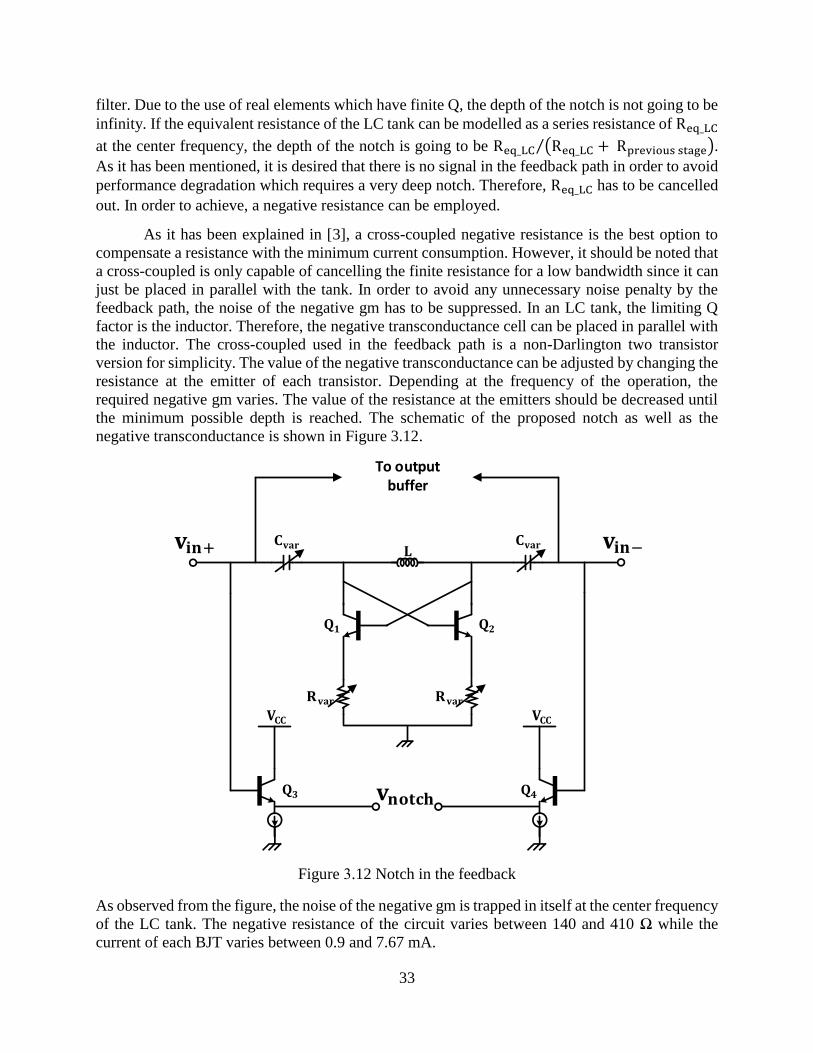
33
filter. Due to the use of real elements which have finite Q, the depth of the notch is not going to be
infinity. If the equivalent resistance of the LC tank can be modelled as a series resistance of Req LC
at the center frequency, the depth of the notch is going to be Req LC (Req LC + Rprevious stage)⁄ .
As it has been mentioned, it is desired that there is no signal in the feedback path in order to avoid
performance degradation which requires a very deep notch. Therefore, Req LC has to be cancelled
out. In order to achieve, a negative resistance can be employed.
As it has been explained in [3], a cross-coupled negative resistance is the best option to
compensate a resistance with the minimum current consumption. However, it should be noted that
a cross-coupled is only capable of cancelling the finite resistance for a low bandwidth since it can
just be placed in parallel with the tank. In order to avoid any unnecessary noise penalty by the
feedback path, the noise of the negative gm has to be suppressed. In an LC tank, the limiting Q
factor is the inductor. Therefore, the negative transconductance cell can be placed in parallel with
the inductor. The cross-coupled used in the feedback path is a non-Darlington two transistor
version for simplicity. The value of the negative transconductance can be adjusted by changing the
resistance at the emitter of each transistor. Depending at the frequency of the operation, the
required negative gm varies. The value of the resistance at the emitters should be decreased until
the minimum possible depth is reached. The schematic of the proposed notch as well as the
negative transconductance is shown in Figure 3.12.
+ −
To output buffer
Figure 3.12 Notch in the feedback
As observed from the figure, the noise of the negative gm is trapped in itself at the center frequency
of the LC tank. The negative resistance of the circuit varies between 140 and 410 Ω while the
current of each BJT varies between 0.9 and 7.67 mA.

34
The output of the notch has to go to a buffer so that the buffer can provide the necessary
current to be subtracted from the input current of the circuit and the feedback loop becomes closed.
The buffer can be a transconductance which provides current when a voltage is applied at its input.
In order to succeed isolation between the feedforward and feedback path, a CASCODE stage is
employed. It is necessary to mention that since the buffer is directly connected to the tank, the
noise of each transistor directly appears at the output of the circuit. This is unavoidable. However,
in order to minimize the noise effect of the circuit, it is desired that the least possible current is
assigned to the buffer while preceding stages are designed to provide a large gain to get high Q.
Depending on the design requirement, the designer can compromise Q for getting better noise
figure. The schematic of the output buffer is shown in Figure 3.13.
To BPF
+ −
Figure 3.13 Output buffer of the feedback path
The current of the circuit should be adjustable so that it can be turned off when the feedback path
is not needed in order to avoid noise figure penalty. For this design, when the circuit is turned on,
the current of each transistor is set to 1 mA.
As mentioned in this section, the proposed band stop filter employs two independent LC
tanks. The center frequency of the tanks can be tuned automatically by monitoring the output of
the band pass filter and notch and change the center frequency until highest possible Q is achieved
while the circuit is stable. However, designing the automatic tuning circuit is beyond the scope of
this research. The schematic simulation of the band pass filter as well as the layout and post layout
simulation will be presented in next chapter.
3.3.2. Band-Stop Filter The schematic of the band stop filter is based on Figure 3.5. For achieving a notch response,
a band pass filter tank is connected to the source of a common source amplifier. If the circuit is
ideal, the circuit output current will be a Q-tunable notch with the depth of infinity. However, due
to the finite Q of the inductor and capacitor, the rejection of the notch is limited to the equivalent
parallel resistance of the tank. Therefore, a negative resistance circuit can be used to compensate
for that. If the negative resistance of the cell is tunable, the depth of the notch can be adjustable
along its frequency range.
In order to implement a negative resistance, the cross-coupled circuit of Figure 3.12 can be
used in CMOS. In the BJT cross-coupled, the assumption is that the transconductance of each

35
transistor is large enough so that the negative resistance is proportional to Rvar. In CMOS, it is not
always practical to assume large transconductance. Therefore, the CMOS version has to be
implemented without the resistance on its source. In this case, the negative resistance of the circuit
is inversely proportional to the transconductance of the transistors. This was not desirable in a
BJT-based circuit due to its heavily nonlinear nature. However, in a CMOS circuit, it is acceptable
not to use degeneration for cross-coupled linearization. The circuit diagram of the notch with the
cross-coupled cell is demonstrated in Figure 3.14.
+ −
Notch Output
Figure 3.14 Preliminary CMOS notch
From the circuit, the frequency of the notch can be varied by changing Cvar and its Q is controlled
by RQ. The negative resistance can also be controlled by changing IBIAS VAR.
The circuit in Figure 3.14 has practical issues which has to be addressed. First, if the biasing
of M1 and M2 is accomplished using a current source, the depth of the notch will be limited by the
output parasitic capacitance of the source. If the source is designed to provide a large current, that
could significantly degrade the performance of the system. In order the avoid this issue, the gate
of the transistor can be biased using the voltage applied at the center tap of the symmetric inductor.
However, since the cross-coupled pair is also biased using the center tap of the inductor, the voltage
needs to be fairly large to give headroom to the cross-coupled in order to avoid saturation. The
voltage is usually set at the highest possible. This causes problem since it leaves no space for M1
and M2 to have positive gate to source bias. To solve bias problem, M3 and M4 can be changed to
PMOS so that they can be biased with a zero voltage at the center tap of the inductor. This leaves
space for the NMOS transistors of M1 and M2 to be biased at a positive voltage. In a CMOS
transistor, the drain current with a square law model is:
ID = μCOX
2
W
L(vGS VTH)2 (3.3.2)
Where μ is the mobility of the channel, COX is the oxide capacitance, W and L are the dimensions
of the transistor, vGS is the gate to source voltage and VTH is the threshold voltage. Therefore, the
transconductance of each transistor is going to be:

36
gm = √2μCOXW
LID (3.3.3)
The value of μ is larger for an NMOS transistor, therefore, in order to provide higher negative
transconductance, an NMOS cross-coupled is preferred. Consequently, the transistors of M1 and
M2 have to be changed to PMOS. Adding a load to the drain of PMOS transistor to get voltage
gain the notch is modified in Figure 3.15.
+ −
+ −
Figure 3.15 Proposed basic circuit of the notch
In order to get a large range of negative resistance, IBIAS VAR has to be dramatically changed since
the transconductance in a CMOS circuit is proportional to the square root of the bias current. This
is unavoidable due to the physical nature of CMOS transistors. Another issue with this circuit, is
in order to get a large Q, RQ has to be increased. This will lead to a large input referred noise and
consequently large noise figure since RQ directly appears at the input of the circuit. Moreover,
since the gain of the circuit is proportional to RD RQ⁄ if transconductance of the transistors is large
enough, the overall gain is going to be small which causes the noise figure of next stages to be
important as well. In order to address the issues mentioned, a low noise amplifier is added before
the notch. The schematic of the proposed low noise amplifier is demonstrated in Figure 3.16.

37
+ −
To Notch
Figure 3.16 Proposed LNA schematic
The proposed LNA without M3 and M4 is called feed forward LNA and it is introduced at [20]. It
can be shown the NF of the feedforward LNA of 3.16 without considering the load and M3 and
M4 is 1 + γ 2⁄ while its NF is 1 + γ without using the feedforward technique. In this case,
matching of 100 Ω is required for each transistor instead of 50 Ω which helps in the power
consumption as well. Adding of M3 and M4 improves the noise performance further by providing
a noise cancelling path to the circuit. The linearity of the circuit can be improved by adding
resistors at the gate source of each common gate transistor. However, that degrades the noise figure
of the system. In this design, no resistor is added due to the importance of noise figure for this
work. The current consumption of each transistor in the LNA design is 1.5 mA while the supply
of the circuit is 3.5 V to get more headroom. As it will be explained in the next chapter, the circuit
can also work with the supply of 2.8 V.
The overall system is based on Figure 3.6 where a feedback is used to enhance the Q of the
system. There are multiple options to implement a negative feedback. However, in order to make
the loop gain and Q adjustable, a common source amplifier with variable bias current is used. The
circuit is implemented using NMOS transistors. The overall schematic of the notch is shown in
Figure 3.17.

38
+ −
+ −
Figure 3.17 The complete schematic of the proposed notch
Based on the figure, the use of differential structures can make it possible to implement a negative
feedback without the need for a separate block for subtraction.
The feedback path and amplifier share the same load of RD. Therefore, the noise of the
feedback amplifiers cannot be suppressed by the LNA regardless of its gain. This adds an
unavoidable noise penalty to the circuit when the feedback path is on. Therefore, the feedback
current is adjustable so that it can be turned off in case the Q that the feedforward path can provide
is sufficient.

39
In order to perform RF testing, the circuits need to be matched to the impedance of the
cables. Therefore, a matched buffer has to be added to the circuit for measurement purposes. Since
linearity is an important factor in this design, the buffer has to be extremely linear. As the process
used in this work is BiCMOS, high current common collector BJT circuits are used to prevent
linearity degradation caused by the buffer. The output of the buffer has to be matched to 50 Ω.
This can be done by adjusting the transconductance of the transistor. However, a more linear
solution is to add a resistor in series with the emitter of the transistor and keep the transconductance
as high as possible. Consequently, the output buffer circuit is designed in a way it consumes 16.4
mA of current which is equally assigned to each output terminal.
As mentioned, the circuit is designed to work at 3.5 V. However, it can also work with 2.8
V supply if a low power operation is desired. With 3.5 V supply, the negative transconductance
branch consumes a current varied between 0 to 9.7 mA. The large range is due to the fact that the
equivalent parallel resistance of the tank varies dramatically in 4 - 8 GHz range where the
minimum is at lower frequencies and since the transconductance of a squared law model device is
proportional to the square root of the current, the large current range is unavoidable. The current
of the feedback is variable between 0 to 1.6 mA where the maximum is for the largest possible Q
and it is off when Q enhancement provided by the feedforward is sufficient. In overall, current
consumption varies between 30 mA and 41 mA where 41 mA is for the case when the lowest
frequency range is desired and the feedback is at its maximum strength. It is important to mention
that 16.4 mA current consumption of the output buffers have to be subtracted from the mentioned
values in order to have a better estimation of current consumption.
The schematic of each proposed circuit has been explained in this chapter. The schematic
simulation and layout and post layout simulations will be presented in next chapter. In the next
section, the linearity of the LC tank as an important part of the linearity of the system is studied
and nonlinear models will be developed in order to gain a better understanding of the nonlinear
mechanisms.
3.4 Linearity Theory The nonlinearity of the tank is a major issue in the nonlinearity of the systems using it. In
a Q-enhanced filter, there are two major sources of nonlinearity. First, the cross-coupled negative
transconductance cell is implemented by transistors as intrinsically nonlinear systems. The
nonlinearity of the negative gm can be easily modelled by power series. Second, the varactor is a
nonlinear element in nature. The nonlinearity of a varactor has a different characteristic than the
nonlinearity of the cross-coupled cell. Since the voltage applied to the varactor determines its
value, any nonlinear mechanism causes changes in varactor value which leads to changes in the
center frequency of the tank. As a result, the circuit experiences a different impedance at the linear
center frequency.
As mentioned, there are two nonlinear elements in a Q-enhanced nonlinear circuit. In this
section, a nonlinear model based on nonlinear feedback is presented to describe the nonlinearity
of the varactor which is also capable of demonstrating the nonlinearity of the negative gm cell. In
order to verify the model, Volterra series nonlinear representation is also presented. There are two
main assumptions in modelling the nonlinearity. First, the nonlinear model is only derived around
the center frequency of the tank. It is assumed that all nonlinear elements not around the center
frequency are rejected by the band pass filter. Second, it is assumed the negative gm cell

40
compensates all the finite equivalent resistance of the tank without changing the series resistance
of it. This way, the tank can be simplified to an ideal tank with a nonlinear negative gm cell.
3.4.1. Nonlinear Feedback Model A varactor is an element with nonlinear C-V characteristics. Without going into the
physical details of it, there are two flat regions and one nonlinear transition region in the
characteristic curve of a varactor. The most nonlinear regions of a varactor are in the transition
region where a small voltage change can cause dramatic capacitance change. It is important to
mention the concept of linearity here is completely different than the linearity of a varactor in a
Voltage Controlled Oscillator (VCO) where the middle of the transition region is considered the
most linear region. In order to characterize the nonlinearity of a varactor, it is necessary to write
Taylor’s series representation of its characteristic curve. By writing the series around the bias point
of the transistor, the first three terms can be represented as:
C(vCONT) = C0 + C1vcont + C2vcont2 (3.4.1)
Where vCONT is the total voltage and vcont is the small signal voltage across the capacitor, C0 is
the linear capacitor, C1 is the first order nonlinear capacitance and C2 is the second order with units
of F V⁄ and F V2⁄ .
The capacitors used as varactors are often small signal capacitors meaning their
capacitance is defined as the change in charge in respect to change in voltage rather than the
absolute value of charge and voltage. In this case, the capacitance is defined as dQ = CdV where
Q is the charge and V is the voltage across the capacitor. Consequently, the current of the capacitor
of equation 3.4.1 can be obtained as:
iC(vcont) =dQC(vcont)
dt= C(vcont) ∙
dvcont
dt
= Co ∙d
dtvcont + C1
2 ∙
d
dtvcont
2 + C23 ∙
d
dtvcont
3 (3.4.2)
As depicted, the equation consists of nonlinear terms of the control voltage and linear derivations
operator. For the complete representation of the current, the series coefficients can be obtained by
taking the derivatives of the C-V characteristics. The characteristic curve can be extracted from
simulation. Using Cadence to run AC simulation and input a capacitor with a voltage or current
source for a single frequency tone, the capacitance can be extracted by calculating i vω⁄ where ω
is the frequency of the simulation. The conceptual C-V characteristic of a varactor is shown in
Figure 3.18.

41
⁄
0
⁄
0
Figure 3.18 Linear and nonlinear coefficients of a varactor
As can be noticed from the figure, C1 sign is always negative or positive (depending on the sign
of vCONT). However, the sign of C2 changes over the control range. As it will be explained later,
this could cause an improvement in the linearity as the coefficients can be set to cancel each other.
The nonlinear model of the capacitor can be applied to the following figure:
Linear Non-linear
Figure 3.19 Varactor nonlinear modeling of an LC tank
The output voltage in this model is the same as the small signal control voltage of the varactor.
The linear impedance of the tank can be calculated as:
Ztank(S) = RP
ω0Q
S
S2+ ω0Q
S+ ω02 (3.4.3)
Where ω0 is the center frequency of the tank in the linear mode and Q is its quality factor. For a
nonlinear system, the output voltage and input current relationship can be modelled as following:
vout = α1is + α2is2 + α3is
3 (3.4.4)
Assuming that the input voltage-current relationship is vs = RPis and by knowing α coefficients,
the 1-dB compression point of the system can be calculated. The nonlinear feedback block diagram
model of the system can be observed in Figure 3.20.

42
Ztank = +
+
Figure 3.20 The nonlinear feedback model of the varactor
As seen from the figure, the nonlinearity of the varactor is modelled using a nonlinear negative
feedback. It is important to gain an intuitive understanding of the nonlinear process before deriving
formulas. Without the feedback, the system acts as a second order RLC network driven by a current
with voltage as the output. If an element (varactor in this case) is nonlinear in the RLC tank, it
starts to create current when a voltage is applied to its terminals and that current may increase or
decrease with the amount of voltage applied to it. The nonlinear current will then be subtracted
from the input current and it flows through the tank again and creates a new output voltage. This
process continues until it reaches a steady state which is the point of interest in this study. At the
steady state, the voltage is no longer equal to its linear case. This can cause gain compression if
the feedback is degenerative. If the feedback is regenerative similar to a VCO, the nonlinear
feedback process continues until it gets saturated, which may cause oscillation. In this study, it is
assumed the strength of negative gm cell is not high enough to start an oscillation.
The nonlinear terms are caused by the interaction of higher order terms in the nonlinear
polynomial equation of the system. If the input of the system is a single tone sinusoidal wave at
the frequency of ω0, a second order term (or a squared term) can cause a tone at the frequency of
2ω0. When the nonlinear terms are sampled at the output and fed back to the input, they see
different impedances of the tank since they are at different frequencies. Therefore, the impedance
of the tank is determined for different frequencies as:
Ztank(ω) =
RP, at 1ω0
j2
3
RP
Q, at 2ω0
RP, at 3ω0
(3.4.5)
It is important to mention that for the third order nonlinearity, only terms around ω0 are of interest;
therefore, it is assumed that the third order terms will later create tones around ω0 by interacting
with 2nd order terms.

43
The term of d dt⁄ is a linear operator and can be replaced by jω0. Applying this, the error
current can be obtained as:
ie = is jω0C1
2vout
2 jω0C2
3vout
3 (3.4.6)
Placing 3.4.4 into 3.4.6 leads to:
ie = is jω0C1
2(α1is + α2is
2 + α3is3)
2
jω0C2
3(α1is + α2is
2 +
α3is3)
3 (3.4.7)
In order to get input-output relationship, the following equation is used:
vout = ie. Ztank(ω) (3.4.8)
where Ztank is obtained from the equation of 3.4.5. By placing 3.4.8 into 3.4.7, α coefficients of
equation 3.4.4 can be found.
When developing the equation for 1-dB compression point, it is important to avoid double
counting of the same terms. If it is assumed the input of the circuit is a single tone current of
ejω0t + e−jω0t, the third order term can be calculated as:
(ejω0t + e−jω0t)3
= ej3ω0t + e−j3ω0t + 3ejω0t + 3e−jω0t =
6 cos𝜔0𝑡 + … (3.4.9)
where 6 cosω0t is the undesired in-band tone created by is3. The interaction between second order
and first order can also create in-band tones. Assuming the second order term is ej2ω0t + e−j2ω0t,
the unwanted terms can be calculated as:
(ejω0t + e−jω0t)(ej2ω0t + e−j2ω0t) + (ej2ω0t + e−j2ω0t)(ejω0t +
e−jω0t) = 2ejω0t + 2e−jω0t + 2ej3ω0t + 2e−j3ω0t = 4 cosω0t (3.4.10)
When the nonlinearity is not created through a feedback process, 3.4.10 terms will not appear.
Therefore, in the new system, both 3.4.9 and 3.4.10 need to be normalized by 6 which leads to
multiplying the second cosine term by 2 3⁄ when calculating 1-dB compression point. Using 3.4.7
and 3.4.8 will lead to:
vout = RPis [1
3(ω0C1)
α12RP
Q] is
2 j [2
3(ω0C1α1α2RP) +
1
3(ω0C2α1
3RP)] is3 (3.4.11)
Comparing the above equation with 3.4.4 results in:

44
αi =
α1 = RP
α2 = −1
3
RP3
Q(ω0C1)
α3 = j (2
9
RP5
Q(ω0C1)
2 1
3(RP
4ω0C2))
(3.4.12)
By applying vs = RPis to 3.4.4, the input-output voltage relationship will be:
vout = α1 vs + α2
vs2 + α3
vs3 =
α1
RPvs +
α2
RP2 vs
2 + α3
RP3 vs
3 (3.4.13)
By knowing Q = ω0RPC0 and employing the 1-dB compression formula of 0.145|α1 α3
⁄ |, the
1-dB compression point in terms of circuit parameters is going to be:
vP−1dB2 =
0.435
Q
C0
C2|1
2
3
C12
C0C2|−1
(3.4.14)
In order to take the nonlinearity of the negative gm cell into account, the system of Figure 3.20
can be modified in to the block diagram of Figure 3.21.
Ztank = +
+
Figure 3.21 The nonlinear feedback model of the tank
In the above figure, the voltage current relationship of the negative gm cell is assumed to be:
45
igm = gm1vout + gm3vout3 (3.4.15)
There are two assumptions in the modeling of equation 3.4.15 in Figure 3.21. First, the linear part
is responsible for compensating the finite Q of the tank. If it completely cancels the equivalent
resistance of the tank, it does not appear in the model. Second, the implementation of the circuit is
differential. Therefore, there is no second order term in the nonlinear modeling of the negative gm
cell. This assumption is not valid for the varactor as its characteristic is not symmetric and the
circuit is not a fully differential pair.
By applying the same procedure as modeling the nonlinearity of the varactor, the
nonlinearity equation of Figure 3.21 will be:
vP−1dB2 =
0.435
Q
C0
C2[(1
2
3
C12
C0C2)2
+ (3gm3
ω0C2)2
]
−0.5
(3.4.16)
In the next section, the same formula will be derived using Volterra series method.
Moreover, verifying Cadence simulations will also be performed to validate the model. Lastly,
tuning strategies will be suggested based on the formula of 3.4.16 to enhance the linearity of the
system.
3.4.2. Volterra Series Model The results obtained from the nonlinear feedback model can also be verified using Volterra
series. A linear system is a system where the output is the scaled version of the input with a transfer
function defined for the system. While the concept of transfer function is only defined for linear
systems, Volterra series is a method to find functions with similar characteristics as a transfer
function for nonlinear terms. Each transfer function is called kernel in Volterra series method.
Since the series is an approximation of a nonlinear function, it is only valid for weakly nonlinear
systems. The weakly nonlinear system is defined by the radius of convergence of the series which
is beyond the scope of this research [21][22].
Without getting too much into the mathematical details of Volterra series, the aim of this
session is to find kernels for the tank of Figure 3.19. The reason for finding kernels is to derive a
closed loop formula for 1-dB compression point of the circuit. There are two major methods to
calculate kernels of Volterra. In the first method, which is also called harmonic method, in order
to find n-th order kernel, the input is assumed to be a linear combination of n single tone signals.
The n tones are then applied to the differential equation of the system. By equating both sides of
the differential equation, the n-th order kernel can be found. While this method is capable of
finding any arbitrary kernel of the system, it may lead to lengthy calculations and it does not
provide any intuition into the nonlinear process taking place in the system. The second method is
called the method of nonlinear currents [23]. The method starts by calculating the first order Kernel
using linear KVL and KCL equations. For higher order Kernels, the nonlinear element is modelled
with a nonlinear current. KVL and KCL can then be written with the nonlinear current in the circuit
to obtain higher order Kernels. The calculation details of this method will be discussed later in this
section.
Starting from the 1st order kernel, it is the same as the linear transfer function. The
equivalent circuit of the 1st order kernel calculation is shown in Figure 3.22.

46
Figure 3.22 First order kernel circuit
As can be observed from the figure, the calculation is done for the Thevenin equivalent circuit of
the tank where C0 is the linear portion of the tank and negative gm cell fully cancelled the
equivalent parasitic resistance of the tank and does not appear at the first order kernel calculations.
By assuming a single tone at the input around the center frequency of the tank ω1, KCL at the
output node leads to:
1− H1(jω1)
RP= H1(jω1)(jω1C0) +
H1(jω1)
jω0L (3.4.17)
The voltages at this equation are normalized to the input voltage and H1(jω1) = vout vs⁄ . The
same method will be used to calculate higher order kernels. At the center frequency of the tank,
first order kernel is going to be:
At ω1: jω1C0 + 1
jω1L= 0 therefore H1(jω1) = 1 (3.4.18)
This is same as the linear transfer function and it states the linear relationship of input and output
for an ideal thevenin second order LC circuit is 1.
In order to calculate the second order kernel, two tones of ω1 and ω2 have to be assumed
around the center frequency of the tank. The second order kernel equivalent circuit is shown in
Figure 3.23.
Figure 3.23 Second order kernel circuit

47
From the figure, the only nonlinear term is iC1 since the negative gm cell is assumed to be perfectly
differential, where even order nonlinearities are zero. The input does not appear in the circuit since
only second order sources have to appear for the second order kernel calculation. The second order
nonlinear current of the varactor can be calculated by applying to tones to the differential equation
of the varactor as:
iC1 = j(ω1 + ω2)C1
2H1(jω1)H1(jω2) (3.4.19)
KCL can then be written at the output node which will lead to:
H2(jω1,jω2)
RP+ H2(jω1, jω2)j(ω1 + ω2)C0 +
H2(jω1,jω2)
j(ω1+ ω2)L+ iC1 = 0
(3.4.20)
By placing 3.4.19 into 3.4.20, the second order kernel can be calculated as:
H2(jω1, jω2) = (ω1+ ω2)2
RP− (ω1+ ω2)2RPLC0+j(ω1+ ω2)L
RPLC1
2 (3.4.21)
It is important to mention for the second order kernel calculation, the frequency is no longer the
center frequency of the tank and inductor and capacitor are not going to resonate with each other.
For the third order kernel, the circuit of Figure 3.24 is used for the calculations.
Figure 3.24 Third order kernel circuit
From the figure, igm3 is just gm3 while iC2
can be calculated using the same method as iC1:
iC2 = j(ω1 + ω2 + ω3)C2
3+ j(ω1 + ω2 +
ω3)C1
2[H1(jω1)H2(jω2, jω3) + H1(jω2)H2(jω1, jω3) +
H1(jω3)H2(jω1, jω2)] (3.4.22)
By assuming all three tones are around center frequency of the tank, the third order kernel can be
obtained as:

48
H3(jω1 = jω1, jω2 = jω1, jω3 = jω2) ≈ RPgm3 j (RPω1C2
3
2
9RPω1
3C12L) (3.4.23)
It is important to note the third order kernel is calculated for the specific case where the frequency
is 2ω1 ω2 rather than calculating it for the most general case since only the tones around the
center frequency of the tank are of concern.1-dB compression point can then be calculated by
applying the following formula:
vP−1dB2 = 0.145
|H1(jω1)|
|H3(jω1,jω1,−jω2)| (3.4.24)
After simplification, 1-dB compression point will be:
vP−1dB2 =
0.435
Q
C0
C2[(1
2
3
C12
C0C2)2
+ (3gm3
ω0C2)2
]
−0.5
(3.4.25)
which is the same as 3.4.16 where 1-dB compression point is derived by applying the nonlinear
feedback modeling.
In order to verify varactor nonlinearity modeling, the nonlinearity of the tank used in the
band pass filter design will be simulated using Cadence. When simulating, the negative gm cell is
assumed to be ideal and linear and it is assumed to compensate the tank in such a way that the
voltage-gain from input to output becomes unity.
Figure 3.25 verification of nonlinear model proposed in this work
As seen from the figure, the nonlinear method can model the nonlinear behavior of the system.
Based on equation 3.4.25, two methods of tuning can be recommended. In method one,
varactor tuning can be accomplished using two different control voltages. This can reduce

49
nonlinear coefficients if each of them is biased in a region where the coefficients can cancel each
other. This method is used at [5]. In method 2, more than one control voltage can be used. For
example, if four control voltages are used, three out of four can be biased at top or bottom flat
regions while the fourth can be used to do continuous frequency tuning [13]. Cadence simulation
for method one leads to the result of Figure 3.26.
Figure 3.26 Dual varactor control simulation
From the figure, up to 14 dB of improvement can be achieved using two varactor control voltages.
The issue with this control scheme is the complexity of automatic tuning implementation since a
look up table is needed in order for the tuning circuit to tune the varactor in order to get the best
possible linearity performance. Four control voltage method can also be simulated. It can be shown
using that method, the linearity of the system becomes limited by the negative gm cell rather than
the varactor. However, using more control voltages is translated into more DC pads which
increases the physical size of the circuit.
3.5 Chapter Summary This chapter is about proposed designs of this work. The chapter starts by introducing the
design requirements for each of the two proposed circuits. Then, the conceptual block diagram of
each design is introduced. The circuit details of each block as well as component values are
presented. At the end of the chapter, two linearity theories are presented to explain the nonlinear
behavior of the LC tank. In the first theory, a nonlinear feedback model is presented using
nonlinear block diagrams. In the second theory, Volterra series method is used to model the
nonlinearity of the varactor as well as the negative gm cell. While the same results are obtained
from both modeling methods, they both are validated by comparing the results extracted from the
models with cadence simulations. Two recommendations are made based on the obtained formulas
from the model.
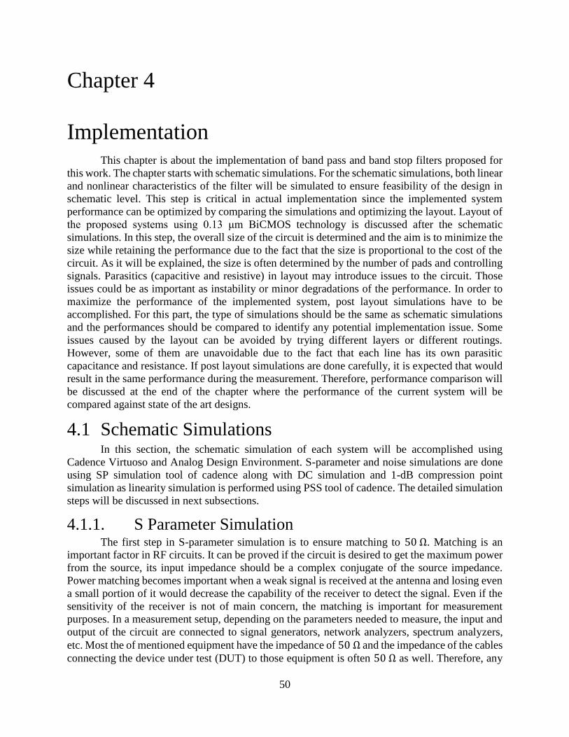
50
4 Chapter
Implementation This chapter is about the implementation of band pass and band stop filters proposed for
this work. The chapter starts with schematic simulations. For the schematic simulations, both linear
and nonlinear characteristics of the filter will be simulated to ensure feasibility of the design in
schematic level. This step is critical in actual implementation since the implemented system
performance can be optimized by comparing the simulations and optimizing the layout. Layout of
the proposed systems using 0.13 μm BiCMOS technology is discussed after the schematic
simulations. In this step, the overall size of the circuit is determined and the aim is to minimize the
size while retaining the performance due to the fact that the size is proportional to the cost of the
circuit. As it will be explained, the size is often determined by the number of pads and controlling
signals. Parasitics (capacitive and resistive) in layout may introduce issues to the circuit. Those
issues could be as important as instability or minor degradations of the performance. In order to
maximize the performance of the implemented system, post layout simulations have to be
accomplished. For this part, the type of simulations should be the same as schematic simulations
and the performances should be compared to identify any potential implementation issue. Some
issues caused by the layout can be avoided by trying different layers or different routings.
However, some of them are unavoidable due to the fact that each line has its own parasitic
capacitance and resistance. If post layout simulations are done carefully, it is expected that would
result in the same performance during the measurement. Therefore, performance comparison will
be discussed at the end of the chapter where the performance of the current system will be
compared against state of the art designs.
4.1 Schematic Simulations In this section, the schematic simulation of each system will be accomplished using
Cadence Virtuoso and Analog Design Environment. S-parameter and noise simulations are done
using SP simulation tool of cadence along with DC simulation and 1-dB compression point
simulation as linearity simulation is performed using PSS tool of cadence. The detailed simulation
steps will be discussed in next subsections.
4.1.1. S Parameter Simulation The first step in S-parameter simulation is to ensure matching to 50 Ω. Matching is an
important factor in RF circuits. It can be proved if the circuit is desired to get the maximum power
from the source, its input impedance should be a complex conjugate of the source impedance.
Power matching becomes important when a weak signal is received at the antenna and losing even
a small portion of it would decrease the capability of the receiver to detect the signal. Even if the
sensitivity of the receiver is not of main concern, the matching is important for measurement
purposes. In a measurement setup, depending on the parameters needed to measure, the input and
output of the circuit are connected to signal generators, network analyzers, spectrum analyzers,
etc. Most the of mentioned equipment have the impedance of 50 Ω and the impedance of the cables
connecting the device under test (DUT) to those equipment is often 50 Ω as well. Therefore, any

51
impedance other than 50 Ω would cause reflection and dependency of the system performance to
the length of the cable. In order to avoid this issue, all ports of the system have to be matched. The
quality of matching at any arbitrary port of “i” is determined by Sii and it is defined as following:
Sii(in dB) = 10 log (Zin,i−50Ω
Zin,i+50Ω) (4.1.1)
Where Zin,i is the input impedance seen at each port. It is usually desired to have Sii of better than
-10 dB.
An issue which has to be addressed before looking into the s-parameter simulation of the
circuit, is that the system designed for this work is a differential circuit, while the measurement
setup will be single ended. Therefore, a single to differential module also called 180 degree hybrid
coupler has to be placed between DUT and measurement instruments. A 180 degree hybrid
coupler is a four terminal device where two of the terminals are connected to DUT, one of them is
connected to a 50 Ω term and the fourth one is connected to the measurement instrument. The
coupler would subtract the DUT signals and feed them to the measurement instrument. Each
terminal of the coupler has to be matched. Therefore, a 1: √2 transformer is used to model the
coupler and realize matching at the input of the circuit in simulations. The schematic is illustrated
in Figure 4.1.
DUTFrom/To measurement
:
Figure 4.1 simulating hybrid coupler using an ideal transformer
As shown in the figure, using an ideal transformer, each port can be matched into 50 Ω.
For matching simulation of the band pass filter, according to the figure, there exist three
ports in our system, port one is the input port, port two is the output port where the band pass
response can be accomplished and port three is the notch monitoring port. As it has been explained,
monitoring the notch is necessary for frequency adjustment to get the highest possible Q from the
system. The matching s parameters of the system is shown in Figure 4.2. As it will be observed
from the figure 4.2, port 1 and port 3 are perfectly matched while port 2 matching is slightly worse

52
than 10 dB. However, since the stage coming after the filter, when implemented in a receiver chain
may not need an output matching, this is not going to be a critical issue. It is also worth mentioning
that the frequency of the notch seen for S11 can vary depending on the frequency the circuit is
tuned at. However, S parameters remain below -10 dB regardless of tuning condition.
Figure 4.2 Schematic matching simulation of the band pass filter
For the matching of the band stop filter, there are two ports in contrast to the band pass
filter where three ports existed in the system. Band stop filter of Figure 3.7 has two ports of input
and output. At the input, an LNA is placed to reduce the noise figure of the system. Based on the
noise and linearity performance, which will be explained in more details in next sections, another
low noise amplifier may be placed before the current system to improve the noise. However, if the
LNA of the proposed system is desired to be placed in direct contact with the antenna, the input
matching will not only be important for measurement purposes, it will also be important to get the
highest possible power from the antenna. Therefore, input matching is critical for this circuit and
it has to be kept below -10 dB. For the output, same as the band pass filter, the matching may not
be as critical as the input. However, for measurement, it is advised to be kept below -10 dB. In this
setup, port 1 is going to be the input while port 2 is the output. The matching of band stop filter is
demonstrated in Figure 4.3.

53
Figure 4.3 Schematic matching simulation of the band stop filter
As can be observed from the figure, both input and output matching are below -10 dB.
Both systems designed as a part of this work are feedback-based systems. A feedback
system with more than two poles has the potential to become unstable. For an analog system, phase
margin is used to determine how stable a system is. Phase margin is defined as the difference of
phase of the loop gain and -180 degrees where the circuit can become unstable. Larger phase
margin is proportional to better stability condition. In RF and microwave circuits, it is more
convenient to use K-stability factor and it is defined as:
K =1− |S11|2− |S22|2+ |Δ|2
2|S11S12| (4.1.2)
Where Δ = S11S22 S12S21. If K is greater than 1, the circuit is stable [24]. From the formula, it
can be understood that K factor can be obtained from S parameter simulation. It is important to
define input and output for the system to get K stability factor. For the band pass filter, input is
going to be port 1. The output of notch is not the main point of concern. Therefore, K factor is
calculated assuming the input is port 1 and output is port 2 where the band pass response is
achieved. The system has the potential to become unstable where feedback is on. Therefore, K
factor is simulated for only when the feedback is on with the highest possible loop gain which has
the highest potential to become unstable. Moreover, the feedback of the band pass filter is
frequency dependent since another LC tank is placed in the feedback loop to get the notch.
Therefore, K factor is simulated for three cases of low frequency which is around 4 GHz, mid
frequency which is around 5-6 GHz and high frequency which is around 8 GHz, the highest
operating frequency of the circuit. The K factor of the band pass filter is depicted in Figure 4.4.

54
Figure 4.4 K stability factor for low frequency (left), mid frequency (middle) and high frequency
(right) of the band pass filter
The low frequency case is where the center frequency of the tank is 4.63 GHz. For this case,
minimum K factor is 50. For mid frequency case, the center frequency is 5.31 GHz and minimum
K is 30. For high frequency case, the center frequency of the band pass filter is 7.62 GHz while
the minimum K factor is 50. As can be concluded from the mentioned results, the circuit is stable
for all cases.
For the band stop filter, the feedback path is not frequency dependent. Therefore, if K factor
is only simulated for one frequency, it can be concluded the circuit will not be unstable. It is
important to mention that the K factor simulation has been performed for all frequency range to
ensure stability. However, only one of the frequencies will be brought here for example. The K
factor simulation of the band stop filter is demonstrated in Figure 4.5.
Figure 4.5 K stability factor for the band stop filter

55
The minimum K for the band stop filter is around 1200 which means the circuit is stable. The K
factor is simulated for the case when the feedback is on and loop gain is at its maximum.
After ensuring the stability and matching, the functionality of each system has to be tested.
For the band pass filter, as it has been explained and demonstrated in Figure 3.3, the Q can be
increased by either increasing the negative transconductance cell in the main path or increasing
the loop gain to increase the Q. For lower Q cases, it is more efficient to increase Q by using the
main path since turning on the feedback path introduces a constant noise to the circuit. As a result,
the Q is increased to until 25 using the main path and negative feedback is used after that to further
increase the Q of the circuit. This test has to be performed for three frequency ranges the same as
simulating the K stability factor. The low Q band pass filter response is shown for three cases of
4.5 GHz, 5.18 GHz and 7.83 GHz in Figure 4.6.
Figure 4.6 Output response of the band pass filter for low Q cases of low frequency (left), mid
frequency (middle) and high frequency (right)
And the high Q response is shown in Figure 4.7.

56
Figure 4.7 Output response of the band pass filter for high Q cases of low frequency (left), mid
frequency (middle) and high frequency (right)
From the figure, the center frequencies are 4.63 GHz, 5.31 GHz and 7.62 GHz respectively while
the Qs are 500, 660 and 600. It will be shown in noise figure simulation in next section that adding
the feedback path impacts the noise figure of the system in about 1 dB. However, this increase
does not change when increasing the Q.
The same simulation for notch has to be done as well. For the first step, the notch has to be
simulated for three frequency ranges as the band pass filter while the feedback path is completely
off. This has been done in Figure 4.8.
Figure 4.8 Output response of the band stop filter for low Q cases of low frequency (left), mid
frequency (middle) and high frequency (right)
And for the high Q case, the simulation results are:

57
Figure 4.9 Output response of the band stop filter for high Q cases of low frequency (left), mid
frequency (middle) and high frequency (right)
The three frequencies are 4.4 GHz, 5.4 GHz and 8 GHz respectively. There is not much
frequency difference between high Q and low Q cases in contrast to band pass filter. For the high
Q case, the feedback is at its highest strength. For high Q-case, a small peaking is noticed.
However, that is not of main concern since the stability of the circuit has already been checked.
As the last part of S parameter simulation, the depth of the notch has to be simulated. As
mentioned previously, the notch is depth, frequency and Q tunable. When the level of the interferer
is not high, a deep notch may not be needed. The depth of the notch can be adjusted by changing
the strength of the negative gm cell. The response of the notch with different depth is highlighted
in Figure 4.10.
Figure 4.10 Notch depth tuning
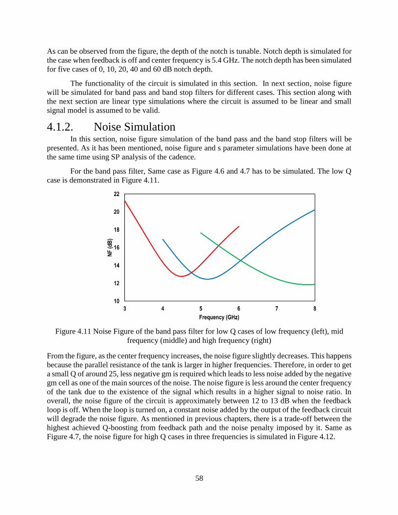
58
As can be observed from the figure, the depth of the notch is tunable. Notch depth is simulated for
the case when feedback is off and center frequency is 5.4 GHz. The notch depth has been simulated
for five cases of 0, 10, 20, 40 and 60 dB notch depth.
The functionality of the circuit is simulated in this section. In next section, noise figure
will be simulated for band pass and band stop filters for different cases. This section along with
the next section are linear type simulations where the circuit is assumed to be linear and small
signal model is assumed to be valid.
4.1.2. Noise Simulation In this section, noise figure simulation of the band pass and the band stop filters will be
presented. As it has been mentioned, noise figure and s parameter simulations have been done at
the same time using SP analysis of the cadence.
For the band pass filter, Same case as Figure 4.6 and 4.7 has to be simulated. The low Q
case is demonstrated in Figure 4.11.
Figure 4.11 Noise Figure of the band pass filter for low Q cases of low frequency (left), mid
frequency (middle) and high frequency (right)
From the figure, as the center frequency increases, the noise figure slightly decreases. This happens
because the parallel resistance of the tank is larger in higher frequencies. Therefore, in order to get
a small Q of around 25, less negative gm is required which leads to less noise added by the negative
gm cell as one of the main sources of the noise. The noise figure is less around the center frequency
of the tank due to the existence of the signal which results in a higher signal to noise ratio. In
overall, the noise figure of the circuit is approximately between 12 to 13 dB when the feedback
loop is off. When the loop is turned on, a constant noise added by the output of the feedback circuit
will degrade the noise figure. As mentioned in previous chapters, there is a trade-off between the
highest achieved Q-boosting from feedback path and the noise penalty imposed by it. Same as
Figure 4.7, the noise figure for high Q cases in three frequencies is simulated in Figure 4.12.

59
Figure 4.12 Noise Figure of the band pass filter for high Q cases of low frequency (left), mid
frequency (middle) and high frequency (right)
The noise figure for high Q cases ranges between 13 to 14 dB which turns into about 1 dB noise
degradation caused by the feedback.
For simulating the noise figure of the notch, it is not necessary to have as many simulations
as the band pass filter. For the band stop filter, the main source of the noise is feedback. There
isn’t any frequency tunable element in the feedback path. Moreover, the in band noise of the
negative gm cell goes to the ground, which is in contrast to the band pass filter. As it has been
mentioned, the band stop filter employs a low noise amplifier at its input. Therefore, it is expected
that the noise figure of the band stop filter would be smaller. The noise figure simulation of the
band stop filter is shown in Figure 4.13. The simulation has been done for two cases of completely
open loop system and maximum feedback strength. From the figure, the noise figure for the lower
band ranges from 4 to 6.6 dB and the noise figure for higher band changes from 5.5 to 7.2 dB. This
is because the CMOS transistors of the technology used are not high performance and
consequently, their performance is not constant along the frequency of operation.

60
Figure 4.13 Schematic simulation of the Noise Figure of the band stop filter for open loop and
closed loop cases
In the next sub-section, 1-dB compression point simulation of the circuit will be presented.
4.1.3. Linearity Simulation The linearity of the system is simulated using PSS analysis of cadence. For linearity test,
1-dB compression point is simulated. The tone for 1-dB compression point simulation has to be
placed at the center frequency of the filter. PSS analysis in contrast to SP analysis is a large signal
analysis meaning the small signal models will no longer be valid.
For the linearity of the band pass filter, the tone is placed around the center frequency of
the tank which is 4.63 GHz. The result is shown in Figure 4.14.

61
Figure 4.14 1-dB compression point simulation of the band pass filter
As seen from the figure, 1-dB compression point is around 6 dBm.
In order to simulate 1-dB compression point of the notch, the tone has to be placed out of
the notch frequency. Linearity of the system is simulated when the feedback path is on as well. As
the center frequency of the tank is set to mid frequency, the tone is placed at 2 and 4 GHz. While
2 GHz may seem far from the operating frequency of the system, it can be a good indication of the
linearity of the system when there is no effect of the notch. The result of 1-dB compression point
simulation is demonstrated in Figure 4.15.

62
Figure 4.15 1-dB compression point simulation of the band stop filter
From the figure, it can be concluded the input 1-dB compression point of the circuit for both 2
GHz and 4 GHz input is around -4 dBm.
In this section, the complete schematic simulation of both systems have been
accomplished. In the next section, the layout of each design will be discussed. After completion
of each layout, the post layout simulation has to be performed and compared to the schematic
simulation of the circuit. This is an iterative process which may take couple of iterations to get the
best layout. The results presented in this chapter are final results and the iterative result of each
step will be skipped.
4.2 Layout of the Designs The size of each layout is often determined by the number of the pads used. The pads are
consisting of signal pads which could be differential and DC pads of supply, ground and control
voltages. Therefore, the first step in each layout is floor planning. If the circuit has different
building blocks, each block can be laid out and tested separately to avoid complexity in debugging
of the system. In this section, the detailed layout of each design will be discussed and the related
pictures will be presented.
4.2.1. Band Pass Filter Layout As mentioned, the first step of the layout is floor planning. For the band pass filter, three
ports are required. Since each port is differential, it has to be in Ground-Signal-Signal-Ground
(GSSG) configuration. Based on the availability of the instruments, pitch of 100 μm is chosen for
each GSSG. If the larger pitch is selected, the size of the circuit is going to be larger while it gives
the benefit of easier probe landing and measurement. Since the input is always connected but port
two and three may not be at the same time, port 1 is placed at the left side of the layout and port 2

63
and 3 will be placed at the right side. This way, each port of 2 and 3 can be measured without the
need to change the measurement setup. Since port 2 and 3 are not going to be used simultaneously,
they can share one common ground to shrink the size of the circuit.
For DC voltages, the frequency of the band pass filter has to be tuned. In order to avoid an
increase in size, only one control voltage is assigned for controlling the varactor associated with
the main path. The voltage of the varactor varies between 1.5 and 3.5 volts and is named VCAP BPF.
If a very small Q is desired, the series resistance of the tank has to be tunable. Therefore, VRQ BPF
is assigned which can be changed from 2.5 to 3.5 volts. The lower voltage corresponds to open
and higher series resistance. While it was not much focused on, there is a trade-off between
linearity and noise for the main band pass filter and it can be adjusted by adjusting the gain.
Therefore, a DC voltage is assigned to change the gain of the main band pass filter. This voltage
is name VAv BPF and it can vary between 0 to 1.8 volts where the highest gain is achieved when the
voltage is set to 1.8. The circuit used as the main band pass filter is the same as [5]. Therefore, it
has its own supply. The supply voltage of the circuit which is named VCC BPF is set to 3.5 volts.
The strength of the negative gm cell in the main path has to be controlled in order to tune the Q.
Therefore, VGM BPF is placed to change the amount of negative gm cell depending on the required
Q from the main path. This voltage varies between 0 to 1.8 volts where 1.8 volts corresponds to
the highest possible strength of the negative gm cell. As it has been mentioned in previous sections,
feedback path may not be needed all the times especially when a low Q is sufficient. In this case,
in order to avoid noise penalty imposed by the feedback path, the path has to be completely turned
off. VON FB is designed to perform this task. This voltage is changed from 0 to 1.8 volts. The gain
of the feedback path has to be tunable in order to achieve Q tunability, therefore, VAv FB is put to
accomplish the mentioned goal. This voltage changes from 0 to 1 volt where 0 corresponds to the
highest possible gain. The feedback path has its own supply of 2.5 volts and its pad name is VCC FB.
The tank of the feedback is also tunable. Since the same tank as the band pass filter is used with a
slightly different configuration to get notch response, VCAP FB is assigned to tune the frequency of
the notch and its voltage varies from 1.5 to 3.5 volts which is similar to the main tank. Lastly, the
notch has its own negative gm cell and its strength is controllable by VGM FB which can be changed
from 0 to 1,8 volts.
The configuration for signal pads is almost predefined. Therefore, three GSSG
configurations are needed. However, for DC pads, it can have multiple configurations. As
mentioned, 10 DC voltages are needed not considering the grounds. Since the left and right of the
layout have already been occupied by GSSG pads, the DC pads have to be placed on top and
bottom of the layout. In order to save space and ease the landing of the probes and avoid probe
collision and based on the availability, a GPPPPPPPPPPG configuration (G for ground and P for
power) is chosen and it is placed on top of the layout. The floor planning of band pass filter is
shown in Figure 4.16.

64
Figure 4.16 Floor planning of the band pass filter layout
As illustrated in the figure, the overall size of the circuit is 675 μm by 1430 μm. It is important to
mention while using a GPPPPPPPPPPG probe facilitates the landing of the probes in terms of
using only one DC probe instead of two, landing of it should be done carefully to ensure all pads
are landed.
As mentioned, it is preferred to design the layout block by block so that the debugging after
post extraction simulation will be more trivial. The layout of the band pass filter has been ready
and it has not been redesigned except the grounding. The layout of the sub circuit of the Figure
3.10 is as following:
Figure 4.17 The layout of the buffer and gain stage of the feedback path
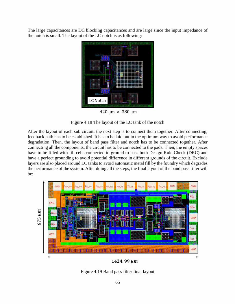
65
The large capacitances are DC blocking capacitances and are large since the input impedance of
the notch is small. The layout of the LC notch is as following:
Figure 4.18 The layout of the LC tank of the notch
After the layout of each sub circuit, the next step is to connect them together. After connecting,
feedback path has to be established. It has to be laid out in the optimum way to avoid performance
degradation. Then, the layout of band pass filter and notch has to be connected together. After
connecting all the components, the circuit has to be connected to the pads. Then, the empty spaces
have to be filled with fill cells connected to ground to pass both Design Rule Check (DRC) and
have a perfect grounding to avoid potential difference in different grounds of the circuit. Exclude
layers are also placed around LC tanks to avoid automatic metal fill by the foundry which degrades
the performance of the system. After doing all the steps, the final layout of the band pass filter will
be:
Figure 4.19 Band pass filter final layout

66
The distance between the output of the band pass filter and the output pad is around 600 μm. This
can cause problem if the line is not matched to 50 Ω. Therefore, by using Sonnet electromagnetic
simulation tool, a 50 Ω transmission line is designed between the output of the band pass filter and
the pads. All adjacent ground pads are connected using the top metal.
4.2.2. Band Stop Filter Layout The layout for the band stop filter, similar to the band pass filter, starts by floor planning.
As it will be explained, the layout of the band stop filter is not as complex as the band pass filter.
Therefore, it is not necessary to do the layout block by block.
For the band stop filter there are two ports of input and output and since both are
differential, two GSSG pads are needed. With the same pitch as the pads of band pass filter, the
input is placed on the right side of the layout while the output is placed on the left side.
For DC control voltages, VSupply is needed. The supply voltage of the circuit varies between
2.8 and 3.5 volts. However, in order to minimize the power at the cost of worse noise figure and
linearity, it is set to 2.8 volts. Since a negative gm cell is employed to control the depth of the
notch, a control voltage is needed for that. Therefore, VGM is assigned to accomplish this task and
it changes from 0 to 2.5 volts. The Q of the system can be controlled by the series resistance of the
LC tank similar to the band pass filter behavior. In order to tune Q, a variable resistance using an
NMOS switch is placed in parallel to the series resistance of the tank and its value can be changed
by changing a voltage called VRQ. This voltage can be changed from 0 to 1.8 volts. In order to tune
the frequency, a voltage control is needed to change the voltage across the varactor. VCAP is
assigned to perform this task and is changeable from 2.5 to 4.5 volts if the supply is 3.5 volts and
1.8 to 3.8 if the supply is 2.8 volts. Lastly, since one way to control the Q is to change the loop
gain, it has to be made variable. Using VFB Av and by changing it from 0 to 2.5 volts, the strength
of the feedback path can be controlled.
So far, there has been two GSSG pads which are placed at the right and left side of the
layout and five control voltages not considering the grounds. While all control voltages can be
placed on top or bottom like the band pass filter, it leads to increase in the overall size of the circuit.
Therefore, two pad sets are used at the top and bottom to shrink the overall size. On the top side,
three of the DC pads are placed in GPPPG configuration. For the remaining DC pads, a GPPG
configuration can be used. However, due to the availability of the probes in the measurement lab
a second GPPPG pad is used. However, since only two control voltages are needed, it will be used
as GGPPG. The floor plan of the band stop filter is shown in Figure 4.20.
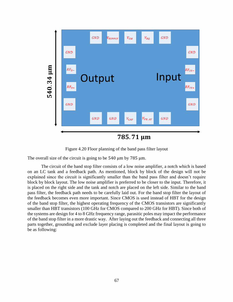
67
Figure 4.20 Floor planning of the band pass filter layout
The overall size of the circuit is going to be 540 μm by 785 μm.
The circuit of the band stop filter consists of a low noise amplifier, a notch which is based
on an LC tank and a feedback path. As mentioned, block by block of the design will not be
explained since the circuit is significantly smaller than the band pass filter and doesn’t require
block by block layout. The low noise amplifier is preferred to be closer to the input. Therefore, it
is placed on the right side and the tank and notch are placed on the left side. Similar to the band
pass filter, the feedback path needs to be carefully laid out. For the band stop filter the layout of
the feedback becomes even more important. Since CMOS is used instead of HBT for the design
of the band stop filter, the highest operating frequency of the CMOS transistors are significantly
smaller than HBT transistors (100 GHz for CMOS compared to 200 GHz for HBT). Since both of
the systems are design for 4 to 8 GHz frequency range, parasitic poles may impact the performance
of the band stop filter in a more drastic way. After laying out the feedback and connecting all three
parts together, grounding and exclude layer placing is completed and the final layout is going to
be as following:

68
Figure 4.21 Final layout of the band stop filter
In this section, the layout of both band pass and band stop filters are discussed along with the
configuration of the pads. This layout has to be matched to the schematic and its parasitic
capacitance and resistance have to be extracted. After this step, post layout simulation is done in
next section and the performance after the layout will be compared with the schematic
performance. If the post extraction is done carefully, the results obtained from post layout
simulation should be close to the results achieved from the actual measurement of the system.
4.3 Post Layout Simulations In this section, the simulation results after parasitic RC extraction of the layout will be
presented. In order to have a fair comparison with the schematic part, same simulation steps will
be followed and the results will be compared with the schematic. In addition to the results
mentioned in the schematic simulation, the power consumption of the circuit will be simulated as
well. After this section, a comparison will be made to the most recent designs in literature.
4.3.1. S Parameter Simulation Same simulations as the schematic simulation will be done for this part. For the band pass
filter, post layout matching is shown in Figure 4.22.

69
Figure 4.22 Post layout matching simulation of the band pass filter
Comparing with Figure 4.2, input and notch matching are still below -10 dB. Output matching is
degraded more is closed to -8 to -9 dB. However, as mentioned before, this is not of main concern.
The same simulations have to be done for the matching of the band stop filter. The results
will be demonstrated in Figure 4.23. From the figure, and by comparing to Figure 4.3 which is the
same simulation for schematic level, it can be concluded the overall matching of the circuit has
not been degraded significantly after post layout simulation. The output matching of the circuit is
slightly better than the input matching. However, as long as both of them are better than -10 dB,
there will be no concerns regarding the matching.
Figure 4.23 Post layout matching simulation of the band stop filter

70
Following the same steps as the schematic simulations, the stability of the systems has to
be studied. It is expected that the stability gets worse for the post layout simulations due to the
existence of layout parasitic poles.
For the stability of the band pass filter, the same simulations as Figure 4.4 has to be done
in three different frequencies. This is shown in Figure 4.24. The simulations are for three different
center frequencies of 4.58 GHz, 5.45 GHz and 7.45 GHz. These three frequencies are slightly
higher than their schematic simulations counterpart. This is due to the unavoidable frequency shift
imposed by the feedback path. As it will be explained, the values of Q are also degraded. The
minimum K factor for the three cases are 5, 7 and 8 respectively. This was expected since the
parasitic capacitance of the feedback play an important role in reducing the stability margin of the
circuit. Although the layout has significantly degraded the minimum K factor of the circuit, the
circuit is still stable since minimum K is larger than unity.
Figure 4.24 K stability factor for low frequency (left), mid frequency (middle) and high
frequency (right) of the band pass filter in post layout simulation
Same as Figure 4.5, the K stability factor for the band stop filter is shown in Figure 4.25.

71
Figure 4.25 K stability factor for the band stop filter after post layout simulations
As compared to the K factor of Figure 4.5, the minimum of K stability factor has been degraded
from 1200 to 28. However, the circuit is still stable.
The output response of the band pass filter for low Q after post layout is going to be:
Figure 4.26 Output response of the band pass filter for low Q cases of low frequency (left), mid
frequency (middle) and high frequency (right) after post layout
And for the high Q case:

72
Figure 4.27 Output response of the band pass filter for high Q cases of low frequency (left), mid
frequency (middle) and high frequency (right) after post layout
Comparing 4.26 with 4.6, the center frequency for low Q cases are 4.41, 5.2 and 7.37 GHz while
the Q for all cases is 25. These frequencies are smaller than the schematic since there is more
parasitic capacitance in the layout. However, frequency shift is in the other direction for high Q
cases as the center frequencies are 4.58, 5.45 and 7.45 GHz for the Qs of 270, 285 and 270. The Q
is almost degraded by half compared to the schematic simulation.
Following the same steps for the band stop filter, the output is going to be:
Figure 4.28 Output response of the band stop filter for low Q cases of low frequency (left), mid
frequency (middle) and high frequency (right) for post layout

73
Figure 4.29 Output response of the band stop filter for high Q cases of low frequency (left), mid
frequency (middle) and high frequency (right) for post layout
The center frequencies are not significantly different than the schematic. It is important to mention
that there are multiple methods to define the bandwidth of a band stop filter. In order to compare
the bandwidth in Figure 4.28 with Figure 4.29, it is assumed the bandwidth is defined at the points
where the gain is 3 dB less than the pass band gain. By defining the bandwidth as mentioned, for
Figure 4.28, bandwidth values from left to right are 180 MHz, 340 MHz and 710 MHz. These
values would be boosted to 80 MHz, 160 MHz and 500 MHz respectively when the feedback is
turned on. The reason the Q enhancement is higher for the lower frequencies is that the maximum
gain the CMOS transistors can provide at higher frequency degrades. If a more advanced CMOS
technology is employed, Q enhancement can be improved significantly.
As the last part of this sub section, the simulation of notch depth is shown in Figure 4.30.
Figure 4.30 Notch depth tuning for post layout

74
As can be seen from the figure, the depth is adjustable from very small values up to about 55 dB.
4.3.2. Noise Simulation The Noise Figure of the cases of Figures 4.26 and 4.27 is simulated in this section. The
results will then be compared to Figures 4.11 and 4.12. It will be shown that the noise degradation
due to post layout is not significant since it is still between 12 and 13 dB same as what has been
observed from Figure 4.11 for the low Q case.
Figure 4.31 Noise Figure of the band pass filter for low Q cases of low frequency (left), mid
frequency (middle) and high frequency (right) for post layout
For the high Q case, the noise figure is shown in Figure 4.32.
Figure 4.32 Noise Figure of the band pass filter for high Q cases of low frequency (left), mid
frequency (middle) and high frequency (right) for post layout

75
From the Figure, the Noise Figure is between 13 to 14 dB which is the same as schematic
simulation. In overall, it can be concluded there is no significant noise degradation in band pass
filter after post layout simulation.
The noise figure simulation for the band stop filter for two cases of open loop and closed
loop is shown in Figure 4.33.
Figure 4.33 Schematic simulation of the Noise Figure of the band stop filter for open loop and
closed loop cases for layout
The Noise Figure is changing from 4.4 to 7.9 dB for open loop and 6.7 to 8.8 for closed loop
simulations. While the Noise Figure degradation is negligible for low frequencies, it is higher than
1 dB for higher frequencies where 6.6 dB of schematic noise figure is compared to 7.9 dB of post
layout for open loop and 7.2 dB of schematic noise figure compared to 8.8 dB of post layout for
closed loop. The reason for this degradation is when more parasitic poles are added to the system,
the gain path will degrade which causes degradation in noise figure since signal is going to be
weaker. If the linearity is still high in post layout simulation, the noise figure can be reduced by
compromising the linearity by adding another low noise amplifier to the system.
4.3.3. Linearity Simulation Linearity simulation of the band pass filter leads to the following Figure for 1-dB
compression point of the circuit.

76
Figure 4.34 1-dB compression point simulation of the band pass filter for post layout
For the band stop filter:
Figure 4.35 1-dB compression point of the band stop filter for post layout
As can be seen the 1-dB compression point of band pass filter is around 2 dBm while this value is
-4 dBm for the band stop filter.
4.3.4. Power Consumption After post layout simulation, the main tank of band pass filter which has the voltage supply
of 3.5 volts consumes between 13.16 mA and 26.8 mA of current while the current of the notch
path varies between 0 to 30.83 mA and the supply of 2.5 volts.
For the band stop filter, DC current ranges from 14 mA to 25 mA and the supply voltage
is 2.8 volts.
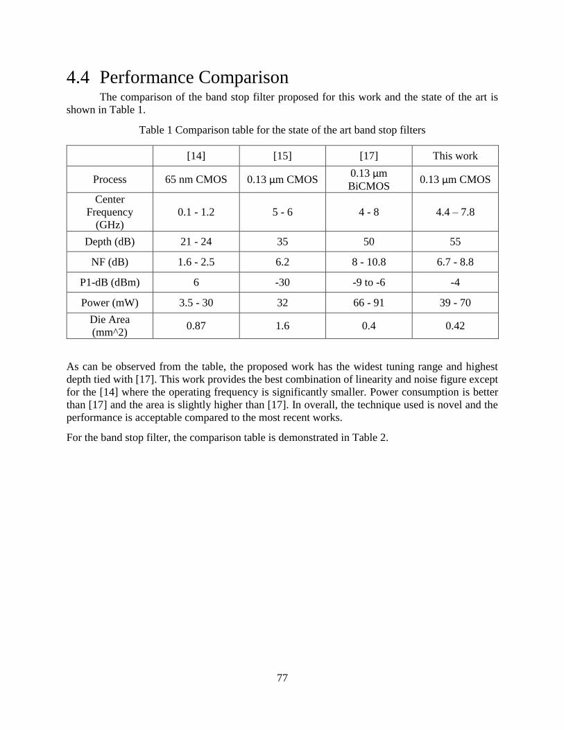
77
4.4 Performance Comparison The comparison of the band stop filter proposed for this work and the state of the art is
shown in Table 1.
Table 1 Comparison table for the state of the art band stop filters
[14] [15] [17] This work
Process 65 nm CMOS 0.13 µm CMOS 0.13 µm
BiCMOS 0.13 µm CMOS
Center
Frequency
(GHz)
0.1 - 1.2 5 - 6 4 - 8 4.4 – 7.8
Depth (dB) 21 - 24 35 50 55
NF (dB) 1.6 - 2.5 6.2 8 - 10.8 6.7 - 8.8
P1-dB (dBm) 6 -30 -9 to -6 -4
Power (mW) 3.5 - 30 32 66 - 91 39 - 70
Die Area
(mm^2) 0.87 1.6 0.4 0.42
As can be observed from the table, the proposed work has the widest tuning range and highest
depth tied with [17]. This work provides the best combination of linearity and noise figure except
for the [14] where the operating frequency is significantly smaller. Power consumption is better
than [17] and the area is slightly higher than [17]. In overall, the technique used is novel and the
performance is acceptable compared to the most recent works.
For the band stop filter, the comparison table is demonstrated in Table 2.

78
Table 2 Comparison table for the state of the art band pass filters
[4] [5] [8] [9] [10] [11] [12] This
work
Process 65 nm
CMOS
0.13 µm
BiCMOS BiCMOS
65 nm
CMOS
65 nm
CMOS
65 nm
CMOS
0.18µm
CMOS
0.13 µm
BiCMOS
Center
Frequency
(GHz)
0.1 - 1 2.25 - 4 0.8 - 2.4 0.6 -
0.85
0.4 -
1.2
0.1 -
1.2 2.03
4.4 –
7.45
Q 3 - 29 3 - 150 5.3 - 16 40 - 90 20 - 60 12.5 -
150 16 3 - 270
NF (dB) 3 - 5 10 - 18.5 19.26 -
21.24 8.6 10 2.8 15 10 - 14
P1-dB
(dBm) 2 -8 to 9
-13 to
-10 0 0 NA -6.6 2
Power
(mW) 2 - 16 43 - 66
350 -
400 75 21.4 15 - 48 16 46 - 171
Die Area
(mm^2) 0.07 0.476 0.15 1.2 0.127 0.27 0.81 0.97
This work has the highest frequency range of all and its tuning range is tied with [5]. The tuning
range of 3 to 270 is the highest of all designs and with the noise figure range of 10 dB to 14 dB
and best case 1-dB compression point of 2 dBm, it provides a reasonable combination of linearity
and noise. The reason for the large size is due to the using of 2 inductors and a complex circuit.
4.5 Chapter Summary This chapter is mainly about the implementation of the two proposed systems of this work.
The chapter starts with schematic simulations of the designs introduced in chapter 3. For each
design, linear simulations of S-parameters, stability and Noise Figure are presented as well as
nonlinearity simulations of 1-dB compression points. Following the schematic simulation, the
layouts of both designs are discussed. For the layout sections, the details of floor planning and
number of control voltages and input and outputs are reviewed. The final layout of each part is
presented along with its overall size. After the layout, the same simulations as the schematic
simulations are demonstrated and the results are compared to schematic simulations. At the end of
the chapter, the performances are compared to the state of the art in band pass and band stop filter
design.

79
5 Chapter
Conclusion This work is based on designing interference cancelling systems for different wideband
and narrowband applications. Filtering is a crucial part of RF communications. In the past, discrete
and mechanical filters were used to accomplish the goal of filtering in high frequency. The new
trend is to design integrated filters aiming to reduce the size and power consumption of the circuit.
Moreover, integrating may provide room for software tuning of the characteristics of the filters.
While current state of the art filter designs have been successful in achieving promising
performances comparable to discrete and mechanical filters, the issue of frequency and bandwidth
tunability is still an ongoing problem. The main purpose of this research is to design cutting edge
filters with outstanding performances and to add frequency and tuning capability to them.
The first design introduced as a part of this work is a band pass filter. The main core of the
filter is based on [5] where a second order RLC tank is employed along with a negative
transconductance cell to enhance the Q of the filter. The issue with [5] is large noise penalty added
to the system for high Q cases. The band pass filter of this research is based on feedback
interference cancelling techniques where the Q of the system can be boosted with minimum noise
penalty. Adding the feedback circuitry to [5] can provide both the advantage of an open loop
system and high Q without excessive noise.
The second design of this work is a band stop filter. The circuit is based on a Q-enhanced
band pass LC tank. The output current of the circuit is controlled by the LC tank and band stop
response can be accomplished by using MOS transistors as transconductances. Feedback is also
used for this design to get sharp transition from stop band to pass band. After final implementation
of the filter, it has the capability of wide frequency tuning as well as depth tuning and bandwidth.
Since an LC tank using a varactor as a variable capacitor in the tank is the main core of
both designs, the linearity of the varactor is a major focus of this study. Using two different
techniques of nonlinear modeling, the nonlinearity of the tank is modelled and schematic
simulations are performed to validate the developed models. After deriving a closed form formula,
different tuning techniques are suggested to enhance the linearity of the system.
There are suggestions for future work that can be done. In this study, the band stop filter
has been implemented using an old technology. Implementing it on a novel CMOS technology in
future research would significantly improve the performance and make it possible to test the idea
for higher frequency ranges. Second, none of the tuning techniques suggested in this work are
implemented in the band stop and band pass filter. Using multiple control voltages or cancelling
nonlinear coefficients by having more than one control voltage can significantly improve the
linearity of the system. Third, there is room to improve the linearity of the negative gm cell. Using
other negative gm generators, the noise and linearity performance of the system can be improved
significantly. Finally, a low noise amplifier (LNA) can be added to the band pass filter. Successful
implementation of an LNA with the band pass filter can give a practical low noise high linearity
receiver.

80
References
[1] J.H. Reed, "Software radio: a modern approach to radio engineering," Prentice Hall
Professional, 2002
[2] Alliance, N. G. M. N. "5G white paper," Next Generation Mobile Networks, White paper, 2015
[3] B. Razavi, "RF Microelectronics (second edition)," Prentice Hall Communications
Engineering and Emerging Technologies Series from Ted Rappaport, 2012
[4] A. Ghaffari, E.A.M. Klumperink, M. Soer, and B. Nauta, "Tunable high-Q N-path band-pass
filters: Modeling and verification," IEEE Journal of Solid-State Circuits, 46, no. 5 p 998-1010,
2011
[5] L. Mohammadi and K-J. Koh, "2–4 GHz Q-tunable LC bandpass filter with 172-dBHz peak
dynamic range, resilient to+ 15-dBm out-of-band blocker," IEEE Custom Integrated Circuits
Conference (CICC), pp. 1-4, 2015
[6] E. Sanchez-Sinencio, "ELEN 622 - Active Filter," Texas A&M
[7] L. E. Franks and I. W. Sandberg, "An Alternative Approach to the Realization of Network
Transfer Functions: The N‐Path Filter," Bell System Technical Journal 39, no. 5: 1321-1350, 1960
[8] Z. Xu, D. Winklea, T. C. Oh, S. Kim, S. T. W. Chen, Y. Royter, M. Lau et al, "0.8/2.2-GHz
Programmable Active Bandpass Filters in InP/Si BiCMOS Technology," IEEE Transactions on
Microwave Theory and Techniques, 63, no. 4: 1219-1227, 2015
[9] N. Reiskarimian and H. Krishnaswamy, "Design of all-passive higher-order CMOS N-path
filters," IEEE Radio Frequency Integrated Circuits Symposium (RFIC), pp. 83-86, 2015
[10] M. Darvishi, R. van der Zee, E.A.M. Klumperink, and B. Nauta. "Widely tunable 4th order
switched g-c band-pass filter based on n-path filters." IEEE Journal of Solid-State Circuits, 47, no.
12: 3105-3119, 2012
[11] M. Darvishi, R. van der Zee and B. Nauta. "A 0.1-to-1.2 GHz tunable 6th-order N-path
channel-select filter with 0.6 dB passband ripple and+ 7dBm blocker tolerance." IEEE
International Solid-State Circuits Conference Digest of Technical Papers (ISSCC), pp. 172-173,
2013
[12] B. Georgescu, I. G. Finvers and F. Ghannouchi, "2 GHz Q-Enhanced Active Filter With Low
Passband Distortion and High Dynamic Range," IEEE Journal of Solid-State Circuits, 41, no. 9:
2029-2039, 2006
[13] F. Amin, S. Raman and K. Koh, "A High Dynamic Range 4th-order 4-8 GHz Q-Enhanced
LC Band-Pass Filter with 2-25% Tunable Fractional Bandwidth," IEEE Int. Microwave
Symposium (IMS), 2016
[14] A. Ghaffari, E.A.M. Klumperink and B. Nauta, "Tunable N-path notch filters for blocker
suppression: Modeling and verification," IEEE Journal of Solid-State Circuits, 48, no. 6: 1370-
1382, 2013

81
[15] A. Vallese, A. Bevilacqua, C. Sandner, M. Tiebout, A. Gerosa and A. Neviani, "Analysis and
design of an integrated notch filter for the rejection of interference in UWB systems," IEEE
Journal of Solid-State Circuits, 44, no. 2: 331-343, 2009
[16] C. C. Cheng and G. M. Rebeiz, "A three-pole 1.2–2.6-GHz RF MEMS tunable notch filter
with 40-dB rejection and bandwidth control," IEEE Transactions on Microwave Theory and
Techniques, 60, no. 8: 2431-2438, 2012
[17] L. Mohammadi and K-J. Koh, "Integrated C-band (4–8 GHz) frequency-tunable &
bandwidth-tunable active band-stop filter in 0.13-µm SiGe BiCMOS," IEEE Int. Microwave
Symposium (IMS), pp. 1-4, 2015
[18] H. Krishnaswamy, P. Kinget and J. Zhou, "WSD: Active Low-Noise Self Interference
Cancellation in Software-Defined Radios," IEEE Radio Frequency Integrated Circuits
Symposium (RFIC) workshops, 2014
[19] H. Darabi, "A blocker filtering technique for SAW-less wireless receivers," IEEE Journal of
Solid-State Circuits, 42, no. 12: 2766-2773, 2007
[20] X. Li, S. Shekhar and D. J. Allstot, "G m-boosted common-gate LNA and differential Colpitts
VCO/QVCO in 0.18-μm CMOS," IEEE Journal of Solid-State Circuits, 40, no. 12: 2609-2619,
2005
[21] A. M. Niknejad, "ECE242: Advanced Integrated Circuits for Communications," UC
Berekeley
[22] P. Wambacq and W. Sansen, "Distortion analysis of analog integrated circuits," Vol. 451.
Springer Science & Business Media, 2013
[23] J. J. Bussgang, L. Ehrman and J. W. Graham, "Analysis of nonlinear systems with multiple
inputs." Proceedings of the IEEE 62, no. 8: 1088-1119, 1974
[24] D. M. Pozar, "Microwave engineering (third edition)," John Wiley & Sons, 2005