filip ronning - slac national accelerator laboratory · prof. zhang was in fact the one who...
TRANSCRIPT

SLAC-586
UC-404(SSRL-M)
AN ANGLE RESOLVED PHOTOEMISSION STUDY OF A
MOTT INSULATOR AND ITS EVOLUTION TO A HIGH
TEMPERATURE SUPERCONDUCTOR*
Filip Ronning
Stanford Synchrotron Radiation Laboratory
Stanford Linear Accelerator Center
Stanford University, Stanford, California 94309
SLAC-Report-586
October 2001
Prepared for the Department of Energy under contract number DE-AC03-76SF00515
Printed in the United States of America. Available from the National Technical Information Service, U.S. Department of Commerce,
5285 Port Royal Road, Springfield, VA 22161
* Ph.D. thesis, Stanford University, Stanford, CA 94309

AN ANGLE RESOLVED PHOTOEMISSION STUDY OF A
MOTT INSULATOR AND ITS EVOLUTION TO A HIGH
TEMPERATURE SUPERCONDUCTOR
a dissertation
submitted to the department of physics
and the committee on graduate studies
of stanford university
in partial fulfillment of the requirements
for the degree of
doctor of philosophy
Filip Ronning
September 2001

I certify that I have read this dissertation and that in
my opinion it is fully adequate, in scope and quality, as
a dissertation for the degree of Doctor of Philosophy.
Zhi-Xun Shen(Principal Adviser)
I certify that I have read this dissertation and that in
my opinion it is fully adequate, in scope and quality, as
a dissertation for the degree of Doctor of Philosophy.
Shoucheng Zhang
I certify that I have read this dissertation and that in
my opinion it is fully adequate, in scope and quality, as
a dissertation for the degree of Doctor of Philosophy.
Ingolf Lindau(Electrical Engineering)
Approved for the University Committee on Graduate
Studies:
iii

Abstract
One of the most remarkable facts about the high temperature superconductors is
their close proximity to an antiferromagnetically ordered Mott insulating phase. This
fact suggests that to understand superconductivity in the cuprates we must first
understand the insulating regime. Due to material properties the technique of an-
gle resolved photoemission is ideally suited to study the electronic structure in the
cuprates. Thus, a natural starting place to unlocking the secrets of high Tc would
appears to be with a photoemission investigation of insulating cuprates.
This dissertation presents the results of precisely such a study. In particular, we
have focused on the compound Ca2−xNaxCuO2Cl2. With increasing Na content this
system goes from an antiferromagnetic Mott insulator with a Neel transition of 256K
to a superconductor with an optimal transition temperature of 28K. At half filling we
have found an asymmetry in the integrated spectral weight, which can be related to
the occupation probability, n(k). This has led us to identify a d-wave-like dispersion
in the insulator, which in turn implies that the high energy pseudogap as seen by
photoemission is a remnant property of the insulator. These results are robust fea-
tures of the insulator which we found in many different compounds and experimental
conditions. By adding Na we were able to study the evolution of the electronic struc-
ture across the insulator to metal transition. We found that the chemical potential
shifts as holes are doped into the system. This picture is in sharp contrast to the case
of La2−xSrxCuO4 where the chemical potential remains fixed and states are created
inside the gap. Furthermore, the low energy excitations (ie the Fermi surface) in
metallic Ca1.9Na0.1CuO2Cl2 is most well described as a Fermi arc, although the high
binding energy features reveal the presence of shadow bands. Thus, the results in
iv

this dissertation provide a new avenue for understanding the evolution of the Mott
insulator to high temperature superconductor.
v

Acknowledgments
The last five years have personally been a wonderful learning experience for many
reasons and due to many people to whom I owe many thanks.
Scientifically, I would like to begin by thanking my advisor, Z.-X. Shen. ZX, has
created an exciting environment for learning and research by creating a lab which is at
the forefront of condensed matter physics and specifically the field of high temperature
superconductivity. Personally, as a first year student I immediately connected with
his inspirational words for the challenging research which lay ahead. I am indebted
to his generous support and encouragement throughout my graduate life. In addition
to ZX, I have received support at some point from what feels like virtually every
member of the Stanford physics and applied physics departments, which is one of the
things I will miss the most about Stanford. In particular I would like to thank Walter
Harrison and Paul McIntyre for being on my committee, and especially Shoucheng
Zhang and Ingolf Lindau for taking up the task of being my other “readers”. Prof.
Zhang was in fact the one who pointing me in ZX’s direction at a time when I was
first seeking some guidance.
Of course, research in ZX’s group, as in most experimental physics pursuits, is
truly a group effort. For all their help and discussions I thank the many Shen group
members whom I have had the privilege of working with: Peter Armitage, Pasha
Bogdanov, Andrea Damascelli, Hiroshi Eisaki, Donglai Feng, Stuart Friedman, Jeff
Harris, Zahid Hasan, Scot Kellar, Changyoung Kim, Alessandra Lanzara, Donghui
Lu, Anne Matsuura, Tchang-Uh Nahm, Anton Puchkov, Kyle Shen, Zhengyu Wang,
Barry Wells, Paul White, Teppei Yoshida, and Xing-Jiang Zhou. In particular,
Changyoung has also acted as an unofficial advisor, and I will forever be grateful
vi

for all his help. Stuart and Paul were the ones who showed me the ropes, back when
I couldn’t pick out swage-lock from pipe thread and had to be told where I could and
could not put my hands on a vacuum chamber. Hiroshi was incredible in providing
help with sample growth. I also have special thanks to the group within the group. In
Andrea, Changyoung, Peter, Donghui, Kyle, and Donglai I have found good friends
from whom I learned a great deal on everything ranging from phonons to the phrase
“Whatzow!”
There was also much help outside the confines of our lab walls for which I am
grateful. I am particularly indebted to the people who provided the samples for this
work. Lance Miller grew 80% of the samples which are presented in this dissertation,
and was always very helpful with all of my requests. Yuhki Kohsaka, Takao Sasagawa,
and Hide Takagi are responsible for providing the Na-doped Ca2CuO2Cl2 samples
which I believe will yield many key pieces of evidence for unlocking the mystery of
high Tc in the coming years. I also thank Walter Hardy, who took me under his wing
when I was rotating with ZX and taught me about penetration depth measurements.
Chris Bidinosti assisted in building a mutual probe in UBC. Transport measurements
which did not yield the results we had hoped for, but made us one experience richer,
could not have been done without the work of Danna Rosenberg. Finally, Mark
Gibson, Gloria Barnes, Marilyn Gordon, and Al Armes were invaluable during my
time here, for their extremely friendly help and willingness to assist in any matter.
This dissertation is also not just the result of five years in the lab. In this regard,
I would also like to thank two of my best friends from Cornell: Anthony Danese
and Shing Yin, who made doing problem sets until the early hours of the morning an
enjoyable experience, not to mention the many good times we had not thinking about
Physics (and I do have the pictures to prove it). I have also learned that the most
enjoyable ice-hockey I have ever played, was not in Canada, but surprisingly turned
out to be in California. Indeed, the ice hockey, soccer, and other activities which I
have enjoyed with my teammates and fellow Stanford classmates has certainly filled
the past five years with many fond memories.
Since the day I was born I have many reasons to thank my family. To my parents
and my brother, Alex, I would like to say: Vielen, vielen Dank! Wegen euch, bin Ich
vii

der Mann ihr sieht heutzutage. Ich konnte es nicht geschaft ohne alle eure hilfe, liebe,
und unterstutzung.
Finally, there is one person who embodies everything for which I am thankful, and
that is my lovely wife, Nicole. She is a part of every aspect of my life. Not only is
she the one cheering the loudest for me and continually inspiring me, but together we
are a team which feels invincible, whether it be in sports, academics, or any obstacles
life has in store for us. She both challenges me and helps me to do the best job
possible. I am so incredibly thankful to have found her. I have never met anyone else
so amazing, and she has made me happier than I ever thought imaginable.
This thesis research was carried out at the Stanford Synchrotron Radiation Lab-
oratory which is operated by the DOE Office of Basic Energy Science, Division of
Chemical Science, the Office’s Division of Materials Science provided funding for this
research.
viii

Contents
Abstract iv
Acknowledgments vi
1 Introduction 1
1.1 A General Overview . . . . . . . . . . . . . . . . . . . . . . . . . . . 1
1.2 Solving High Tc . . . . . . . . . . . . . . . . . . . . . . . . . . . . . . 6
1.3 Doping Evolution . . . . . . . . . . . . . . . . . . . . . . . . . . . . . 13
1.4 System of Choice . . . . . . . . . . . . . . . . . . . . . . . . . . . . . 16
2 ARPES 19
2.1 Photoemission Energetics . . . . . . . . . . . . . . . . . . . . . . . . 19
2.1.1 Measuring the Chemical Potential . . . . . . . . . . . . . . . . 21
2.2 ARPES . . . . . . . . . . . . . . . . . . . . . . . . . . . . . . . . . . 23
2.3 Correlations and Approximations . . . . . . . . . . . . . . . . . . . . 24
2.3.1 Sudden approximation versus the adiabatic limit . . . . . . . . 28
2.4 Analysis methods . . . . . . . . . . . . . . . . . . . . . . . . . . . . . 30
2.4.1 n(k) . . . . . . . . . . . . . . . . . . . . . . . . . . . . . . . . 30
2.4.2 MDC analysis . . . . . . . . . . . . . . . . . . . . . . . . . . . 30
2.4.3 Matrix elements . . . . . . . . . . . . . . . . . . . . . . . . . . 32
2.5 Practical issues . . . . . . . . . . . . . . . . . . . . . . . . . . . . . . 33
3 Remnant Fermi Surface/d-Wave-Like Dispersion 37
3.1 Background . . . . . . . . . . . . . . . . . . . . . . . . . . . . . . . . 38
ix

3.2 Experimental . . . . . . . . . . . . . . . . . . . . . . . . . . . . . . . 39
3.3 Methodology for analyzing the data . . . . . . . . . . . . . . . . . . . 40
3.4 Results from an insulator . . . . . . . . . . . . . . . . . . . . . . . . . 43
3.5 Implications of a remnant Fermi surface in a Mott insulator . . . . . 51
4 Electronic Structure of a CuO2 plane 54
4.1 Introduction . . . . . . . . . . . . . . . . . . . . . . . . . . . . . . . . 54
4.2 Experimental . . . . . . . . . . . . . . . . . . . . . . . . . . . . . . . 56
4.3 Sr2CuO2Cl2 and Ca2CuO2Cl2 . . . . . . . . . . . . . . . . . . . . . . 56
4.4 Ca2CuO2Br2 . . . . . . . . . . . . . . . . . . . . . . . . . . . . . . . . 58
4.5 Bi2Sr2ErCu2O8 and Bi2Sr2DyCu2O8 . . . . . . . . . . . . . . . . . . . 60
4.6 Sr2Cu3O4Cl2: Cu3O4 plane . . . . . . . . . . . . . . . . . . . . . . . . 63
4.7 La2−xSrxCuO4, Nd2CuO4, and Other Cuprates . . . . . . . . . . . . . 67
4.8 Discussion . . . . . . . . . . . . . . . . . . . . . . . . . . . . . . . . . 67
5 A Detailed Study of A(k, ω) at Half Filling 70
5.1 Experimental . . . . . . . . . . . . . . . . . . . . . . . . . . . . . . . 72
5.2 Eγ Dependence on E(k) and n(k) . . . . . . . . . . . . . . . . . . . . 72
5.2.1 Eγ Discussion . . . . . . . . . . . . . . . . . . . . . . . . . . . 83
5.3 Rounded Node . . . . . . . . . . . . . . . . . . . . . . . . . . . . . . 88
5.3.1 Dispersion Discussion . . . . . . . . . . . . . . . . . . . . . . . 91
5.4 Conclusions . . . . . . . . . . . . . . . . . . . . . . . . . . . . . . . . 93
6 Na-doped Ca2CuO2Cl2 94
6.1 Experimental . . . . . . . . . . . . . . . . . . . . . . . . . . . . . . . 95
6.2 Valence Band Comparison . . . . . . . . . . . . . . . . . . . . . . . . 95
6.3 Shadow bands . . . . . . . . . . . . . . . . . . . . . . . . . . . . . . . 99
6.4 Chemical potential shift . . . . . . . . . . . . . . . . . . . . . . . . . 102
6.4.1 Eγ dependence versus the Insulator . . . . . . . . . . . . . . . 106
6.5 Fermi Surface Arc . . . . . . . . . . . . . . . . . . . . . . . . . . . . . 107
6.6 Lineshapes and Dispersion . . . . . . . . . . . . . . . . . . . . . . . . 109
6.6.1 Temperature dependence of the peak-dip-hump . . . . . . . . 116
x

6.6.2 Self Energy, Σ . . . . . . . . . . . . . . . . . . . . . . . . . . . 117
6.7 Doping Evolution . . . . . . . . . . . . . . . . . . . . . . . . . . . . . 120
6.8 Temperature Dependence . . . . . . . . . . . . . . . . . . . . . . . . 121
6.9 Discussion with other Cuprates . . . . . . . . . . . . . . . . . . . . . 124
6.10 Conclusions . . . . . . . . . . . . . . . . . . . . . . . . . . . . . . . . 130
7 Conclusions and Future Prospects 132
7.1 Half-filling . . . . . . . . . . . . . . . . . . . . . . . . . . . . . . . . . 132
7.2 x�=0 . . . . . . . . . . . . . . . . . . . . . . . . . . . . . . . . . . . . 133
7.3 What Remains . . . . . . . . . . . . . . . . . . . . . . . . . . . . . . 134
Bibliography 136
xi

List of Figures
1.1 Crystal structure of A2CuO2Cl2 (A=Sr,Ca) . . . . . . . . . . . . . . . 2
1.2 Historical perspective of the maximum superconducting Tc . . . . . . 3
1.3 Cartoon of Angle Resolved Photoemission . . . . . . . . . . . . . . . 5
1.4 Phase diagram of the cuprates . . . . . . . . . . . . . . . . . . . . . . 7
1.5 Band structure results . . . . . . . . . . . . . . . . . . . . . . . . . . 9
1.6 Cartoon of a Zhang-Rice singlet . . . . . . . . . . . . . . . . . . . . . 12
1.7 n(k) for the Hubbard and t-J models . . . . . . . . . . . . . . . . . . 13
1.8 Doping evolution for band, Mott, and charge-transfer insulators . . . 14
1.9 Alternative scenarios for doping a Mott insulator . . . . . . . . . . . 16
2.1 Energetics of the photoemission process. . . . . . . . . . . . . . . . . 21
2.2 Experimentally determining µ by photoemission . . . . . . . . . . . . 22
2.3 Cartoon of band mapping by ARPES . . . . . . . . . . . . . . . . . . 25
2.4 Photoemission from a hydrogen molecule: A comparison between the
sudden and adiabatic limits. . . . . . . . . . . . . . . . . . . . . . . . 29
2.5 Effects of charging on photoemission spectra. . . . . . . . . . . . . . . 35
3.1 Illustration of the Fermi surface determination. . . . . . . . . . . . . 40
3.2 Fermi surface determination for Bi2212 and La3−xSrxMn2O7 . . . . . 42
3.3 ARPES spectra and n(k) plots on various cuts from Ca2CuO2Cl2 . . 44
3.4 A) and B) n(k) comparison of Ca2CuO2Cl2 to Bi2212. C) and D)
Dispersion of Ca2CuO2Cl2 . . . . . . . . . . . . . . . . . . . . . . . . 46
3.5 Cartoon comparing half-filling to optimal doping . . . . . . . . . . . . 48
3.6 High energy pseudogap comparison with the insulator . . . . . . . . . 50
xii
4.1 ARPES spectra of Sr2CuO2Cl2 and Ca2CuO2Cl2 . . . . . . . . . . . . 57
4.2 ARPES spectra of Ca2CuO2Br2 . . . . . . . . . . . . . . . . . . . . . 59
4.3 Polarization dependence of Bi2Sr2ErCu2O8 valence band . . . . . . . 60
4.4 ARPES spectra and second derivative plot of Bi2Sr2ErCu2O8 . . . . . 61
4.5 ARPES spectra and second derivative plot of Bi2Sr2DyCu2O8 . . . . 62
4.6 Cartoon comparison of CuO2 and Cu3O4 unit cells . . . . . . . . . . 64
4.7 Valence band spectra of Sr2Cu3O4Cl2 at high symmetry points . . . . 65
4.8 ARPES spectra of Sr2Cu3O4Cl2 . . . . . . . . . . . . . . . . . . . . . 66
4.9 Temperature dependence of Bi2Sr2ErCu2O8 valence band spectra . . 68
4.10 Comparison of the various half-filled cuprates . . . . . . . . . . . . . 69
5.1 Eγ dependence on Ca2CuO2Cl2 EDCs along Γ → (π, π) . . . . . . . . 74
5.2 Ca2CuO2Cl2 E(k) dependence on photon energy . . . . . . . . . . . . 75
5.3 Ca2CuO2Cl2 EDCs along Γ → (π, π) using 16.5eV to 17.5eV photons 76
5.4 An example of an asymmetric spectral intensity about (π/2, π/2) in
Ca2CuO2Cl2 . . . . . . . . . . . . . . . . . . . . . . . . . . . . . . . . 77
5.5 Eγ dependence of n(kx=ky) in Ca2CuO2Cl2 . . . . . . . . . . . . . . . 78
5.6 Eγ dependence of n(k) over the entire Brillouin zone . . . . . . . . . 80
5.7 ARPES spectra from the n(k) mappings of Ca2CuO2Cl2 . . . . . . . 82
5.8 Comparison of E(k) and n(k) dependence on Eγ ‖ and ⊥ to the anti-
ferromagnetic zone boundary . . . . . . . . . . . . . . . . . . . . . . . 83
5.9 Cartoons to illustrate differing ideas of the remnant Fermi surface . . 86
5.10 ARPES spectra of Ca2CuO2Cl2 along (π, 0) to (0, π) . . . . . . . . . 89
5.11 d-wave comparison of the detailed E(k) of Ca2CuO2Cl2 . . . . . . . . 90
5.12 Parameterizing the flattened dispersion near (π/2, π/2) . . . . . . . . 91
6.1 Valence band comparison of Ca2CuO2Cl2 and Ca1.9Na0.1CuO2Cl2 along
the nodal direction . . . . . . . . . . . . . . . . . . . . . . . . . . . . 97
6.2 Time dependence of Ca2−xNaxCuO2Cl2 valence band spectra . . . . . 98
6.3 Overview of spectral features in Ca1.9Na0.1CuO2Cl2 . . . . . . . . . . 100
6.4 Comparison of EDCs between 10% Dy-doped Bi2212 and 10% Na-
doped Ca2CuO2Cl2 . . . . . . . . . . . . . . . . . . . . . . . . . . . . 101
xiii

6.5 Dispersion of x=0 compared to x=0.10 of Ca2−xNaxCuO2Cl2 . . . . . 103
6.6 EDC comparison of the metal to the insulator . . . . . . . . . . . . . 105
6.7 Photon energy dependence comparison of the metal to the insulator . 106
6.8 Fermi surface of Ca1.9Na0.1CuO2Cl2 . . . . . . . . . . . . . . . . . . . 108
6.9 Two component structure in the EDCs near (π/2, π/2) . . . . . . . . 109
6.10 MDC analysis of Ca1.9Na0.1CuO2Cl2 . . . . . . . . . . . . . . . . . . . 111
6.11 Photon energy dependence of Ca2−xNaxCuO2Cl2 EDCs . . . . . . . . 112
6.12 Photon energy dependence of Ca2−xNaxCuO2Cl2 MDCs . . . . . . . . 113
6.13 The MDCs derived dispersion for Eγ=16.5 and 21.0eV . . . . . . . . 115
6.14 Temperature dependence of the peak-dip-hump in Ca2−xNaxCuO2Cl2 116
6.15 Temperature dependence of the MDC derived dispersion along kx=ky 117
6.16 Self Energy of Na-doped Ca2CuO2Cl2 . . . . . . . . . . . . . . . . . . 119
6.17 Fermi surface mappings of Ca2−xNaxCuO2Cl2 as a function of doping 120
6.18 EDCs of x=0.12 Na-doped Ca2CuO2Cl2 . . . . . . . . . . . . . . . . 122
6.19 Nodal direction temperature dependence of Ca2−xNaxCuO2Cl2 . . . . 123
6.20 Temperature dependence of the leading edge midpoint near the edge
of the Fermi arc in Ca2−xNaxCuO2Cl2 . . . . . . . . . . . . . . . . . 124
6.21 Theoretical Fermi surfaces obtained for a CuO2 plane . . . . . . . . . 129
xiv

Chapter 1
Introduction
1.1 A General Overview
Understanding high temperature superconductivity is an extremely complex and in-
teresting problem. In this section I will introduce this subject by reviewing some of
the basic properties of the high temperature superconductors. The remainder of this
introduction will present a more detailed picture of the current state of the field, and
will identify the specific questions which this dissertation addresses.
In normal materials a single electron will bump into other electrons over a million
times a second, but in superconducting materials, electrons have amazingly found a
way to avoid one another entirely. This dissertation is one part of a global effort to
understand how this phenomenon occurs in a particular class of materials called the
cuprates.
The term cuprates is used to describe all ceramic crystals that have the common
feature of layers of copper and oxygen atoms. (See figure 1.1) Before the discovery
of superconductivity in La2−xBaxCuO4 in 1986,[1] superconductivity could only be
found below 23 degrees Kelvin (-250C)[2] (see figure 1.2). In the cuprates, transitions
into the superconducting state have now been found as high as 138K(-135C) under
atmospheric conditions,[3] and can be pushed even higher by applying pressure to
the sample. The dramatic increase in transition temperature compared to previously
known crystals gave these materials the title of ”high temperature superconductors”.
1
Chapter 1. Introduction 2
Cu2+
Ca,
O
Apical Halide2+
2-
Sr,2+ Na+
Figure 1.1: Crystal structure of A2CuO2Cl2 (A=Sr,Ca), a typical cuprate. By substi-tuting Na for Ca one can create a high temperature superconductor. The complicatedstructure on the left can be simplified by considering only the CuO2 layers as relevant,and the remaining atoms, called charge reservoir layers, simply provide or remove elec-trons from the CuO2 planes. Due to the two dimensional nature of the cuprates thestructure can be further reduced to a simple single CuO2 unit cell shown on the right.
Although, to put this in perspective, this temperature still lies 46◦C below the coldest
temperature ever recorded on Earth(Antartica in 1983).[4] In 1956 J. Bardeen, L.N.
Cooper, and J.R. Schrieffer developed a model now known as BCS (after their last
names), which explains superconductivity from a microscopic point of view for the
lowest temperature superconductors.[5] However, under this theoretical framework
superconductivity at “high” temperatures is inconceivable. Obviously, a new micro-
scopic understanding is necessary. Over the past 15 years more research has been
Chapter 1. Introduction 3
1900 1920 1940 1960 1980 20000
20
40
60
80
100
120
140
160
180
200
liquid N2
Coldest Recorded Temperature
Hg-Ba-Ca-Cu-O
Tl-Ba-Ca-Cu-O
Bi-Sr-Ca-Cu-O
Y-Ba-Cu-O
La-Ba-Cu-O
Nb3Ge
Nb3SnNbN
NbPbHg
TC (
K)
Year of Discovery
Figure 1.2: A historical perspective of the rising maximum superconducting tran-sition temperature. “High Tc” began with the discovery of superconductivity inLa2−xBaxCuO4.[1] The dotted red line indicates the boiling point of liquid nitrogen,a relatively cheap coolant. For perspective the lowest temperature recorded on theearth’s surface (in Antartica, 1983) is also indicated. (Figure courtesy of D.H Lu)
done in this field than in any other area of physics. Despite many accomplishments,
the fact that we still lack an understanding of the cuprates hints at the complexity
of this problem.
The cuprates actually come in many varieties. One way to characterize them is by
the average number of conduction electrons per copper atom. Conduction electrons
are those electrons which are able to move throughout the solid. By chemically substi-
tuting the atoms which surround the copper-oxygen layers the number of conduction
electrons can be changed. Remarkably, when there is an average of one conduction
Chapter 1. Introduction 4
electron per copper atom, as in Ca2CuO2Cl2 (Calcium copper oxychloride), the ma-
terial is an electrical insulator; however, Ca1.85Na0.15CuO2Cl2, for example, has an
average value of 0.85 conduction electrons per copper atom and becomes supercon-
ducting at low enough temperatures. [See figure 1.4] To find that the best conductors
of electricity to date are so closely related to insulators was one of the most shocking
discoveries in this field.
Aside from the fundamental interest of this problem to physicists, the cuprates also
have great technological potential. It is hoped that by understanding the microscopic
mechanism of the cuprates, scientists will be able to synthesize new materials which
superconduct at room temperature and above. One could then easily exploit their
fantastic characteristics. For example, since superconducting electrons do not collide
with one another, they will not lose any energy. As a result, one could use energy much
more efficiently, and a natural consequence would be that the cost of electricity would
drop. Superconductors also have the potential to be great magnets, leading to, among
other things, faster trains, better computers, and more powerful scientific probes
including those used for medical diagnosis. In fact, anything that uses electricity or
magnetism has the potential for improvement. It should be noted that while some
applications may be more of a dream than potential reality, others are already in
use. As an example, high temperature superconductors are playing a large role in
improving cellular phones.
How then does one begin to attempt to understand the cuprates? For physicists,
one of the most important properties of a material is something called its electronic
structure. This structure contains a wealth of information, describing the physical
properties, such as the energy and momentum, of every electron inside the solid. From
this microscopic knowledge, many macroscopic physical properties can be understood.
Among other things, one can predict the color of a material, whether or not it is
fluorescent, transparent, or shiny, and how well it can conduct electricity. In fact,
all physical properties including superconductivity are dependent on the electronic
structure of a material in some way. For example, in the BCS model, in order to
calculate the temperature at which the electrons will begin to superconduct, one
needs to know the energy distribution of the electrons; this information is contained

Chapter 1. Introduction 5
E(k)
Sample
ElectronAnalyzer
Photon Source
Monochromater
Figure 1.3: A schematic of Angle Resolved PhotoEmission Spectroscopy(ARPES).While a synchrotron facility is often the preferred light source, there are many alter-natives. The wavelength of light is chosen by a monochromator. The photons arethen absorbed by the sample and electrons are thus emitted. An electron analyzermeasures the Kinetic energy of the out going electrons. From the position of thedetector and using the fundamental conservation laws of energy and momentum, onecan then extract the dispersion relation E(k) which gives the energy of an electroninside the sample as a function of its momentum. (For details see chapter 2)
in a materials electronic structure. So to discover the microscopic nature of the
high temperature superconductors, a good starting point would be to determine the
electronic structure of the cuprates.
The technique of Angle Resolved Photoemission (ARPES) is ideally suited for
this task. The origin of this technique can be traced to Hertz’s discovery of the
photoelectric effect.[6] By shining light with sufficient energy on a material, electrons
are emitted from the surface. We can detect the energy and momentum of these
out going electrons. Then by using fundamental laws of physics, we can deduce
the energy and momentum distribution of the electrons from when they were in the
sample, thereby directly probing its electronic structure. For a schematic illustration
of ARPES, see figure 1.3. Thus, by performing ARPES on cuprates we hope to
determine any peculiarities in their electronic structure that would result in such
high transition temperatures into the superconducting state.
This dissertation presents ARPES results on cuprates such as Ca2−xNaxCuO2Cl2
and related materials. I will demonstrate how the electronic structure changes when
a cuprate goes from an insulator to a superconductor. In following this evolution, I
Chapter 1. Introduction 6
have noticed that certain features of the electronic structure are remarkably similar
in both the insulator and the superconductor. We hope that this will provide a guide
to the theorists in developing a new theory of superconductivity.
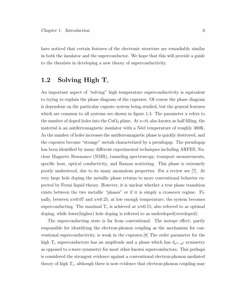
1.2 Solving High Tc
An important aspect of “solving” high temperature superconductivity is equivalent
to trying to explain the phase diagram of the cuprates. Of course the phase diagram
is dependent on the particular cuprate system being studied, but the general features
which are common to all systems are shown in figure 1.4. The parameter x refers to
the number of doped holes into the CuO2 plane. At x=0, also known as half filling, the
material is an antiferromagnetic insulator with a Neel temperature of roughly 300K.
As the number of holes increases the antiferromagnetic phase is quickly destroyed, and
the cuprates become “strange” metals characterized by a pseudogap. The pseudogap
has been identified by many different experimental techniques including ARPES, Nu-
clear Magnetic Resonance (NMR), tunneling spectroscopy, transport measurements,
specific heat, optical conductivity, and Raman scattering. This phase is extremely
poorly understood, due to its many anomalous properties. For a review see [7]. At
very large hole doping the metallic phase returns to more conventional behavior ex-
pected by Fermi liquid theory. However, it is unclear whether a true phase transition
exists between the two metallic “phases” or if it is simply a crossover regime. Fi-
nally, between x≈0.07 and x≈0.25, at low enough temperature, the system becomes
superconducting. The maximal Tc is achieved at x≈0.15, also referred to as optimal
doping, while lower(higher) hole doping is referred to as underdoped(overdoped).
The superconducting state is far from conventional. The isotope effect, partly
responsible for identifying the electron-phonon coupling as the mechanism for con-
ventional superconductivity, is weak in the cuprates.[8] The order parameter for the
high Tc superconductors has an amplitude and a phase which has dx2−y2 symmetry
as opposed to s-wave symmetry for most other known superconductors. This perhaps
is considered the strongest evidence against a conventional electron-phonon mediated
theory of high Tc, although there is now evidence that electron-phonon coupling may
Chapter 1. Introduction 7
T
AFI
d-wave SC
“strange” metal
x0 0.05 0.15
“normal” metal
Optimal doping
Underdoped Overdoped
Half-filled
Figure 1.4: A simplified phase diagram of the cuprates. At half filling the cuprates areantiferromagnetic insulators(AFI). As holes are doped into the CuO2 plane (increasingx) the system becomes a poor metal, which has been characterized by many unusualproperties. At very large hole doping more typical metallic properties associated witha Fermi liquid exist. The hashed line indicates the ambiguity as to whether there isa true phase transition between the two metallic regimes, or whether it is simply acrossover of differing energy scales. Red is the region of superconductivity, and someterminology is indicated at the bottom.

Chapter 1. Introduction 8
not necessarily compete against d-wave superconductivity [9, 10]. It should also be
noted that the weak isotope effect is not an open and shut case either. Crawford et
al.[11] showed using the LSCO and LBCO systems that there exists a considerable
doping dependence of the isotope effect which is greatest when the LTO to LTT struc-
tural phase transition is maximal. Aside from the electron-phonon coupling question,
attempts to explain superconductivity given any coupling mechanism within the con-
ventional BCS framework have failed [12]. The phase diagram is further complicated
when considering electron doping to the CuO2 plane(ie x<0; not shown). Qualita-
tively it appears symmetric with respect to half filling, but a closer inspection reveals
that this symmetry is only approximate. The antiferromagnetic phase is more robust,
and superconductivity is limited to a smaller doping range than on the hole doped
side. The symmetry or lack thereof is crucial to theories of high temperature super-
conductivity. Although many implicitly assume an electron-hole symmetry there is
clearly much to be understood on this issue.
The crystal structure of the cuprates at first glance is even more complicated
than the phase diagram. However, both experiments and theory agree that the low
energy physics of the cuprates is dominated by the CuO2 planes, which are common
to all cuprates. Thus the crystal structure can be thought of as layers of CuO2 planes
separated by charge reservoir layers, the details of which simply act to supply more or
less holes into the CuO2 plane. The extreme two dimensional nature of the cuprates
means that theoretically, we can focus our attention on a single CuO2 plane. This is
illustrated in figure 1.1. In this case the three relevant orbitals are the oxygen px, py
and copper dx2−y2 orbitals. Performing a simple tight binding calculation, one gets a
nonbonding band (Ek = εp) as well as bonding and antibonding bands of the form
Ek =εp + εd
2±
√(∆
2)2 + 4tpd(sin
2 kxa
2+ sin2 kya
2) (1.1)
where tpd is the hopping integral from a copper d orbital to a neighboring oxygen
p orbital, εp and εd represent the energy of putting an electron on the respective
orbitals, ∆ = εp − εd is the charge transfer energy, and a is the lattice constant. At
x=0 there are 5 electrons per unit cell to fill these bands, which results in a half-filled

Chapter 1. Introduction 9
antibonding band as shown in figure 1.5. A more complete band calculation also finds
a metal resulting from the CuO2 plane.[13] However, this is wrong! Experimentally, at
half filling these crystals are insulators with a charge gap of roughly 1.5 to 2eV.[14, 15]
Clearly, electron correlations which are neglected in the band calculations must be
taken into account. Specifically, the insulating nature is a result of the energy cost,
U, associated with putting two electrons in the copper dx2−y2 orbital. This can be
qualitatively understood by considering a chain of hydrogen atoms as described by
-6
-4
-2
0
2
4 tpd = 1.4eV
εp - εd = 3.5eV
B
NB
AB
Ener
gy
(eV)
(0,0) (0,0) (0,0) (0,0)(π,0) (π,π) (π,0) (π,π)
Figure 1.5: Band structure along high symmetry directions. Left is a simple tightbinding model using only Cudx2−y2 , Opx, and Opy orbitals as a basis. The relevantparameters are indicated in the figure. Right is the complete band structure calcula-tion of Ca2CuO2Cl2 using the linear augmented plane-wave method.[13] Clearly bothpredict a metal at half-filling.

Chapter 1. Introduction 10
Mott.[16] Band theory predicts the chain to be metallic independent of the separation
between atoms. However, in the limit of large atomic separation the electrons will
be localized on each atom resulting in an insulating state. As the hopping integral
becomes infinitesimally small at large separation, it is no longer valid to ignore the
energy associated with putting two electrons on a single atom (since it is comparable
to the kinetic energy, proportional to t). In the cuprates, the Cu d orbitals are highly
localized; hence, large atomic separation is not necessary for electron correlations to
be relevant.
Theoretically, we need a model which can capture the physics at hand. We begin
with one of the simpler models, the one band Hubbard model[17], which was first
argued by Anderson to capture the essential properties of the cuprates.[18]
H = t∑σ〈ij〉
(c†iσcjσ + H.c.) + U∑
i
ni↑ni↓ (1.2)
where c†iσ creates an electron with spin σ on the ith site of a square lattice (for now the
oxygen sites have been ignored). The first sum is over nearest neighbor sites 〈ij〉 only,
t is the effective hopping integral, U is the energy cost of putting two electrons on the
same site, and niσ=c†iσciσ is the electron occupation operator This simple Hamiltonian
is deceptively complex, and has only been solved for special cases. At half filling and
U=0 one recovers the tight-binding result, while for t=0, one can see that the ground
state is 2N degenerate with a single, localized electron per site. Since for large U ,
doubly occupied sites are energetically very costly, one can project out the doubly
occupied states for small t/U and arrive at an effective Hamiltonian, known as the
t-J model:
H = t∑σ〈ij〉
(c†iσ cjσ + H.c.) + J∑〈ij〉
(Si ·Sj − 1
4ninj)−
t2
U
∑σ〈ijk〉
(c†kσnj−σ ciσ − c†kσ c†j−σ cjσ ci−σ + H.c.) (1.3)
where ciσ = ciσ(1− ni−σ) is an electron creation operator which prevents double
occupation, J=4t2/U , Si=c†iασijcjβ with σij being the Pauli spin matrices, and where

Chapter 1. Introduction 11
the final term is a three site term which is usually neglected. Note that although c†iσrepresents the creation of an electron when possible, it no longer satisfies the fermionic
commutation relations. At half filling, hopping is not possible as every site contains
one spin, and double occupancy is not allowed. Thus for x=0, the t-J model reduces
to a spin 1/2 Heisenberg antiferromagnet. Indeed the half filled cuprates are one of
the best experimental realizations of the spin 1/2 Heisenberg antiferromagnet with
J=130meV determined by neutron and two magnon Raman scattering [19, 20].
However, photoemission experiments have shown that the Cud8 state is 8eV below
the Cud9L state, where L refers to the ligand(which in this case are the oxygen
atoms).[21] This is large with respect to ∆, and classifies the cuprates as charge
transfer insulators(∆ < U) rather than Mott insulators(∆ > U). Thus it is not
clear whether or not one may neglect the oxygen sites when constructing an effective
Hamiltonian for the low energy physics. So Emery proposed the more comprehensive
three band Hubbard model[22]:
H = εd
∑iσ
ndiσ + εp
∑jσ
npjσ + tpd
∑σ〈ij〉
(p†jσdiσ + H.c.) + tpp
∑σ〈jj′〉
(p†jσpj′σ + H.c.)+
Ud
∑i
ndi↑n
di↓ + Up
∑j
npj↑n
pj↓ + Upd
∑σ〈ij〉
ndiσn
pj−σ (1.4)
where p and d refer to oxygen p and copper d orbitals, respectively. Unfortunately, it
is not apparent how one reduces this Hamiltonian to the one band Hubbard model.
However, the pioneering effort by Zhang and Rice has made this Hamiltonian a man-
ageable starting place.[23] They applied the three band Hubbard model to a single
CuO4 cluster containing two holes (see figure 1.6). They found that one hole located
on the Cu site would hybridize most strongly with a hole located on a linear combina-
tion of the four surrounding oxygen hole states forming what they termed a singlet, a
nonbonding, and a triplet state. The large energy separation between the singlet and
the triplet, which has been calculated by Eskes and Sawatzky to be 3.5eV,[24] implied
that the triplet state could be projected out. Note that the Zhang-Rice singlet states

Chapter 1. Introduction 12
Figure 1.6: From ref. [23]. Schematicof the hybridization of a hole on theCu site with a hole on the four sur-rounding oxygens.
on neighboring sites are not orthogonal. An effective Hamiltonian can then be con-
structed to allow the “Zhang-Rice singlet” to hop over the entire CuO2 plane. The
impressive result is that the effective Hamiltonian is again the t-J model, which was
also the effective Hamiltonian for the single band Hubbard model. In this sense, it
is tempting to think of the Zhang-Rice singlet as forming an effective lower Hubbard
band, thus lending more credibility to starting from an effective one band Hubbard
model to begin with. Finally, we note that the one band Hubbard model possesses
electron hole symmetry while the three band Hubbard model does not which is rel-
evant in trying to understand the electron doped as well as hole doped side of the
phase diagram.
Early angle resolved photoemission results on Sr2CuO2Cl2 showed that the Hub-
bard model is indeed a reasonable starting point.[25] The overall bandwidth is sim-
ilar to the t-J prediction of 2.2J , which contrasts to the 8tpd prediction from band
theory. The discrepancy however lies in the dispersion from (π, 0) to (π/2, π/2)
The t-J model predicts all the states along the antiferromagnetic zone boundary,
(π, 0) to (0, π), to be degenerate. However, the actual dispersion is on the or-
der of the total band width. The solution to this problem has been to add sec-
ond and third nearest neighbor hopping terms, t′ and t′′ which lifts this degeneracy
[26, 27, 28, 29, 30, 31, 32, 33, 34, 35, 36].

Chapter 1. Introduction 13
Figure 1.7: From ref. [37]. Spectral weight(proportional to the radius of the circle)from exact diagonalization calculations of 16, 18, and 20 site clusters of the one bandHubbard (left) and t-J (right) models. U/t=10.
1.3 Doping Evolution
Although the Hubbard models correctly predict an antiferromagnetic insulator at
x=0 it is still unclear how the Mott insulator evolves across the metal to insulator
transition. For a material where band theory is valid, it is known that the Fermi
surface will shrink to a point and then disappear. For a Mott insulator though it
is still unknown. This is the main question which this dissertation addresses. The
Fermi surface is one of the most characteristic properties of a metal. How, then, does
it vanish as a system becomes an insulator? Numerical calculations show that in the
intermediate coupling regime of the Hubbard model, the occupation probability, n(k),
survives in the insulating state, while this is not true in the t-J model.[37, 38, 39](See
figure 1.7) Chapters 3 and 5 will investigate this issue from the experimental point of
view of angle resolved photoemission.
Alternatively, one can flip the question around, and ask how the insulator evolves
to the metal. In particular, how does the chemical potential shift upon doping? First
let us compare a band insulator, a Mott-insulator and a charge-transfer insulator
(shown in figure 1.8). Upon doping the band insulator with either holes or electrons

Chapter 1. Introduction 14
the chemical potential simply shifts. The Mott-insulator is similar, but with one
significant difference: when a hole is doped into the system it removes one doubly
occupied state. This is a state in the upper Hubbard band. A state from the lower
Hubbard band is also removed. Hence, spectral weight is transferred from the upper
and lower Hubbard bands as the chemical potential shifts to the lower hubbard band.
The situation is analogous when an electron is doped into the system. For a charge-
transfer insulator, the electron doped picture remains the same, although note that
the spectral weight which is lost still comes from the lower Hubbard band, not the
2N 2N
2N
2N 2N+1
2N-11
1
N N
N-1 N-1
N-1 N-1
2
2
N N2N
2N-11
N N
2NN-1 N-12
Semi-Conductor Mott-Hubbard Charge-Transfer
µ
µ
µ
µ
µ
µ
µ
µ
µ
U U∆
Figure 1.8: The effect of doping three kinds of insulators: A band-insulator, a Mott-insulator, and a charge-transfer insulator. The electron removal spectra (ie. photoe-mission) are indicated by the shaded regions, while the electron addition spectra (ie.inverse photoemission) are dotted. The top shows the undoped insulator while themiddle and bottom spectra are for a single doped hole or electron, respectively. (afterref [40])

Chapter 1. Introduction 15
charge transfer band. In the case of hole doping, an occupied state in the charge
transfer band simply becomes unoccupied, and nothing else happens. This is what
happened in the case of the band insulator. Thus there is a distinct asymmetry
between the effects of hole doping and electron doping. The charge-transfer scenario
was drawn in the limit of negligible hopping (tpd → 0). As the hybridization is
increased between the oxygen p and copper d orbitals, the charge-transfer band will
also transfer spectral weight, and thus look increasingly more like the lower hubbard
band[40]. Thus we again recover a scenario which appears more like the one band
Hubbard model out of the original charge-transfer insulator.
The above description however, fails to capture another possibility which appears
to have been realized in the cuprates. Namely, in the case of La2−xSrxCuO4 it is
believed that the chemical potential remains fixed inside the gap upon doping [41].
These states are presently believed to be related to stripe formation.[42] The addi-
tional scenario along with the case described above is shown in figure 1.9. Again,
we start at half filling where the chemical potential in the absence of any impuri-
ties is undefined as the energy to add an electron greatly differs from the energy to
remove an electron. However, upon doping one can imagine that states are created
which fix the chemical potential inside the gap. This is a strongly differing view from
the case where the chemical potential shifts upon doping. Note that in the scenario
where states are created inside the gap, it is assumed that by doping the system, one
changes the Hamiltonian of the system. Otherwise, this scenario is not possible. In
chapter 6 we will present ARPES results on Ca2−xNaxCuO2Cl2, which in contrast to
La2−xSrxCuO4, shows that the chemical potential shifts with doping akin to a band
material. We will discuss the remarkable finding that two similar systems could show
differing evolutions across the metal insulator transition.
Studying the evolution across the metal to insulator transition has also allowed
us to make several interesting observations on the origin of various aspects of the
electronic structure in the cuprates. Throughout this dissertation we will demon-
strate that the high energy pseudogap as seen by ARPES is indeed a property of the
insulator. This was first conjectured to be the case by Laughlin.[44] Furthermore,
in chapter 3 we find that the dispersion of the insulator can be characterized by a

Chapter 1. Introduction 16
µ
µ
µ
Ueffa)
b)
c)
Figure 1.9: Two possible evolutions of the chemical potential upon hole doping.a)The undoped Mott insulator. b) The chemical potential shifts upon doping causinga transfer of spectral weight. c) Doping creates states inside the gap which are filled.(After ref. [43])
d-wave like modulation, the details of which will be investigated in chapters 4 and
5. Thus, an interesting link between the antiferromagnetic insulator and the d-wave
superconductor is formed. A consequence of the chemical potential shift observed
in chapter 6 is the existence of shadow bands[45] in a hole doped sample; however,
the low energy excitations appear more well described as a Fermi arc[46] than as a
hole pocket centered about (π/2, π/2) as one would naively expect. We will conclude
with a discussion on some of the theoretical implications of our results, and other
prospects for future work in this exciting field.
1.4 System of Choice
As mentioned earlier, the cuprates come in many varieties. While each are unique in
their own way, they all share the common feature of CuO2 planes. So the first task is

Chapter 1. Introduction 17
to decide which system will be the most effective in answering the questions discussed
above. Bi2Sr2CaCu2O8+δ, with its high transition temperature and extremely good
cleavage plane, is almost the ideal system for photoemission. It has only a few minor
drawbacks. First is the presence of “superstructure” caused by a modulation in the
BiO layer, which clouds the interpretation of the data near (π, 0). The second is the
relatively poor spectral quality of the data as half filling is approached. The reason
for this is unclear, but may be due to the sample quality. This is a significant set back
for trying to address the issues concerning the metal to insulator transition. There
have been two approaches to fill this void. One is to study the La2−xSrxCuO4 system
which is grown equally well over the entire doping range. Unfortunately, it does not
have a very good cleavage plane, and the resulting spectra are also quite broad.1 The
alternative approach is to study the oxyhalide system, which until very recently had
not been successfully doped to produce single crystals. The later approach has been
taken in this dissertation.
The oxyhalide compounds, M2CuO2X2 (M=Sr,Ca,Ba; X=F,Cl,Br) and variations
thereof have been known since the 1970’s. For a review of the various structures see
ref [49]. The compound Sr2CuO2Cl2 is considered one of the best realizations of the
S=1/2 Heisenberg quantum antiferromagnet [50, 51]. The difference of these single
layer cuprates to others is the presence of an apical halide as opposed to an apical
oxygen for other hole doped cuprates. The discovery of superconductivity in the
oxyhalide, Sr2CuO2F2.6 (Tc=46K), suggested that the apical site was not intimately
connected with hole doped superconductivity [52]. Indeed we find, that the electronic
structure is independent of the apical atom (See chapter 4). The good cleavage plane
of the oxyhalides makes them a potentially ideal system to study with photoemission.
Indeed the ARPES data on (Sr,Ca)2CuO2Cl2 produces the highest quality spectra
from any half filled cuprate.[25, 26, 53, 54, 55] This facilitates a comparison across
the metal insulator transition with data from the Bi2Sr2CaCu2O8+δ system. After
attempts by many institutions, Kohsaka et al. have successfully produced hole doped
single crystals of Ca2−xNaxCuO2Cl2 [56]. The photoemission study of this compound
1Recent measurements on La2−xSrxCuO4 are now revealing sharper structure when the experi-mental conditions are properly tuned.[47, 48]

Chapter 1. Introduction 18
is presented in chapter 6. With the oxyhalide systems and the technique of angle
resolved photoemission we are now ideally prepared to tackle the issues of the insulator
to metal transition in the cuprates.

Chapter 2
ARPES: a technique to probe the
electronic structure
Angle Resolved Photoemission (ARPES) is a powerful tool for studying the electronic
structure of solids. Its origin can be traced back to Hertz’s discovery of the photo-
electric effect in 1887,[6] which was subsequently explained under the postulates of
quantum mechanics by Albert Einstein in 1905.[57] Today it is used in condensed
matter physics to probe the electronic structure of solids.
2.1 Photoemission Energetics
To illustrate the usefulness of photoemission to solid state physics we begin by demon-
strating how the electronic density of states can be obtained from a photoemission
experiment. In a photoemission experiment we illuminate a sample with monochro-
matic light of energy, hν. If this energy is greater than the work function of a material
then an electron will be emitted. Conservation of energy tells us that
Efinal = Einitial + hν (2.1)
Efinal(Einitial) is the final(initial) state of the entire N particle system. The final state
is a product of a free electron and the remaining N-1 particle system, ΨN−1. If we
19

Chapter 2. ARPES 20
assume a single particle picture, as is often done (although we will reexamine this
point shortly), then the energy of the N particle system can be described as the sum
of N individual states: EN =∑
k εk. Thus one will see that EN = εk + EN−1. So
equation 2.1 can now be rewritten as:
Ep.e. + EN−1 = EN + hν (2.2)
Ep.e. = εk + hν (2.3)
where p.e. stands for the photoelectron. Taking the chemical potential to be the zero
of energy we get
KEp.e. + Φ = εk + hν (2.4)
where KE is the kinetic energy of the emitted electron, and Φ is the work function
of the sample. If we further assume that the cross section for emitting an electron
is independent of it’s initial state and final momentum1 then we can see that the
ratio of the number of electrons emitted with KEA versus the number of electrons
emitted with KEB will be equal to the number of states at energy εk = KEA +
Φ − hν divided by the number of states at energy εk = KEB + Φ − hν. Thus it
is apparent that a photoemission spectra I(KE) will be proportional to the density
of electronic states which are occupied. This is illustrated in figure 2.1. In practice
these spectra, also known as angle integrated spectra, are obtained by collecting a
finite solid angle of electrons emitted from a polycrystaline surface. Note that in
the figure the photoemission spectra has additional weight indicated by the hashed
region. These electrons are termed secondary electrons and result from those which
incur multiple scattering events, and thus lose a fraction of their energy inside the
solid before they are emitted.
1This is an unjustified assumption. We will in see subsequent sections that photoemission crosssections have a large k dependence. Thus, one should always be wary of detailed fits to angleintegrated data.
Chapter 2. ARPES 21
Einitial
Efinal
Φ
EF
EVac
KineticEnergy
BindingEnergy
hν
Density of States
E
Figure 2.1: Energetics of the pho-toemission process showing howphotoemission maps out the den-sity of states. The hashed re-gion is due to “secondary” elec-trons which are the result of mul-tiple scattering events. Φ is thework function, and hν is the pho-ton energy.
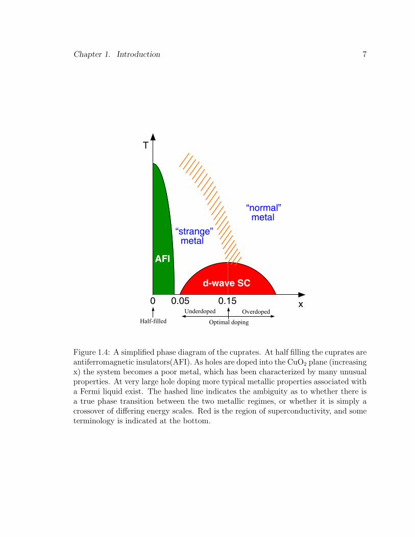
2.1.1 Measuring the Chemical Potential
From above we can see that the electron with the maximum kinetic energy will orig-
inate from the highest occupied orbital. However, one would often like to know
whether this electron lies at the chemical potential, or alternatively, if there is an
energy gap in the system. As work functions are not very precisely known, the ques-
tion of calibrating one’s photoemission spectra is an important yet subtle one. To
do so, we must first understand precisely what is measured in the experiment. An
illustration of this process is shown in figure 2.2. It is important that the sample and
the detector are in electrical contact, so that the chemical potential of the two will
be equal. It is entirely possible that the work functions of the two are different. In
this event a potential, VS−D, will be established between the sample and the detector.

Chapter 2. ARPES 22
KEinit KEmeasured
VS-D
ΦdetectorΦsample
µ µ
Sample Detector
Figure 2.2: An illustration of the energies involved in determining a reference energyin photoemission. Note that a potential VS−D is created to account for the differencein work functions between the sample and the detector. For this reason the chemicalpotential as measured for two different samples will be the same.
This prevents a violation to the law of conservation of energy. Otherwise, one can
see that if the work function of the sample and the detector are different, then in
the absence of the potential VS−D, an electron would lose an amount of energy =
Φsample when emitted by the sample and gain an energy = Φdetector �= Φsample when
absorbed by the detector. The potential, VS−D, causes the measured kinetic energy
to be different from the kinetic energy which the electron had as it left the sample by
an amount VS−D. Therefore the energy of the free electron can now be written as
Ep.e. = KEinit + Φsample = KEmeasured + Φdetector (2.5)
Thus using equation 2.3 we get
Einitial = KEmeasured + Φdetector − hν (2.6)
The importance of this is to note that the relevant work function is that of the
detector, and not of the sample. Thus, independent of what sample is emitting the
electrons, so long as the the detector is in electrical contact with the sample, the
reference point will be the same. In our case, we use a polycrystaline sample of gold
in electrical contact to form a reference. The acquired photoemission spectra from

Chapter 2. ARPES 23
the gold sample is fit to the Fermi-Dirac function:
I(KEmeasured) ∝ 1
(1 − exp (Einitial − µ)/kT(2.7)
where k is Boltzmann’s constant and T is the temperature of the gold sample. The fit
gives us the kinetic energy of an electron at the chemical potential = µ−Φdetector +hν,
which is independent of the sample being measured. Thus we can study a sample of
interest with the chemical potential predetermined by our gold reference. From now
on we will no longer make the distinction between the measured kinetic energy and
the kinetic energy of the electron as it is emitted from the sample. This distinction
was only necessary to understand how one can identify the chemical potential in a
photoemission experiment. On a side note, the fit to the Au spectra will also give us
a measure of our experimental energy resolution.
2.2 ARPES
We now turn our attention to Angle Resolved Photoemission. So far we have only
used the conservation of energy and have neglected the conservation of momentum.
In the photoemission process the component of momentum perpendicular to the sur-
face is not conserved; although there is a one-to-one correspondence of k⊥ inside the
sample to k⊥ outside the sample. A simple way to think of this is that the work
function creates a potential perpendicular to the surface, and thus a force is applied
in this direction to the electron as it escapes from the solid. As a result, momentum
conservation is no longer valid. However, assuming that the surface barrier is uni-
form across the sample, the inplane component of momentum is conserved up to a
reciprocal lattice vector G.
ki‖ + kγ‖ = kpe‖ + ksystem‖ + G‖ (2.8)
where the momentum of the photon, kγ , can be ignored for low photon energies (for
hν=20eV; |k|=0.01A which is roughly 1% of the Brillouin zone in cuprates). To
extract the inplane component of momentum one uses:

Chapter 2. ARPES 24
kpe‖ = kpesinθ =
√2meKE
hsin θ = 0.512
√E
A−1
eV
kpex = kpe‖ cos φ ; kpey = kpe‖ sin φ (2.9)
ARPES becomes even more powerful when studying one- or two-dimensional sys-
tems, since in this instance the dispersion is fully characterized by k‖ which, con-
trary to k⊥, is conserved in the photoemission process. Figure 2.3 demonstrates how
ARPES can be used to determine the electronic structure by again examining a sys-
tem of non-interacting particles, this time in two dimensions. The electron analyzer
measures the kinetic energy of the outgoing electron. From the position of the ana-
lyzer, the angles θ and φ are also known. From these two pieces of information and
using equations 2.4 and 2.9 the energy of the state εk is uniquely determined. By
changing the position of the analyzer relative to the surface normal the entire k-space
can be mapped out to give the full dispersion. Figure 2.3 also illustrates the typical
fashions in which photoemission data is presented. Kinetic energy scans at constant θ
and φ are called energy distribution curves (EDCs). Note that as long as the kinetic
energy range of the scan is small compared to the kinetic energy, then curves which
are taken at constant (θ, φ) are equivalent to a hypothetical scan taken at constant
(kx, ky). Alternatively, the energy can be held constant and the angle can be var-
ied. The resulting curves are known as momentum distribution curves (MDCs).[58]
In both cases the peak position of a curve gives us εk while the peak width gives
information on the interactions as will be discussed below.
2.3 Correlations and Approximations
Now having a general feel for the concepts used in photoemission we will construct
here a more formal approach to the subject. For a detailed derivation the reader is
referred to more comprehensive works such as the one by Almbladh and Hedin and
references therein [59]. In this way we can also begin to take electron correlations into
account. There are several approximations used in analyzing photoemission spectra
and for many of them there appears little justification other than the fact that the

Chapter 2. ARPES 25
k α sin θ (φ=0)
Ene
rgy
E
kx
ky
EF
EF
EF
Fermi surface n (k)
θφ
a) b)
MDC’s
ED
C’s
Figure 2.3: ARPES is an ideal technique for probing the electronic structure. Thisillustration assumes a non-interacting two dimensional electron gas shown in (a). Thedetector in photoemission measures the kinetic energy and angle of the photoemittedelectron. By scanning energy and changing angles one can generate an intensity plotas shown in (b) (yellow is maximum intensity). Using standard conservation laws thethe energy and momentum of the photoelectron yields the energy and momentum ofthe initial state from which it came. By performing many two dimensional cuts asthe one shown in (b) for different φ angles, one can reconstruct the full dispersioninformation presented in (a). The red and blue curves illustrate typical ways inwhich ARPES data is presented known as EDCs and MDCs respectively. The curvescorrespond to slices taken out of the neighboring image plot along the thin lines. Bytracking the peak position one can again recreate the dispersion seen in (a), in thiscase for ky=0.
resulting equations manage to describe the experimentally measured spectra quite
well. Specifically, we will work under the sudden approximation, where it is assumed
that the electron is removed quickly enough from the sample so that the system is
unable to adiabatically evolve into its new state.
Calculating the photoemission intensity is equivalent to determining the cross-
section for starting in an initial N particle state ΨNi and ending in a N particle final
state ΨNi which consists of a photoemitted electron and the remaining N-1 particle

Chapter 2. ARPES 26
system. This can be expressed as:
σfi =2π
h|〈ΨN
f |Hint|ΨNi 〉|2δ(EN
f − ENi − hν) (2.10)
This is the perturbative result where the bare Hamiltonian consists of the system
alone, and the delta function ensures energy conservation. In the presence of elec-
tromagnetic radiation the momentum operator changes from p → (p − ecA). For a
system where the potential terms only depend on x and not on p
H = Hsystem + Hint (2.11)
where
Hint =e
2mec(p · A − A · p) +
e2
c2A2 (2.12)
For current photoemission experiments, the amplitude, |A|, of the incident light is
small enough that one can ignore two photon processes and hence drop the A2 term.
Furthermore, if the wavelength of light is large compared to atomic dimensions then
one can use the commutation relation [p,A] = −ih∇ · A ≈ 0. Thus Hint reduces toe
mecA · p and the cross section can now be expressed as
σfi ∝ |〈ΨNf |A · p|ΨN
i 〉|2 (2.13)
This is commonly referred to as the dipole approximation. We note that there
is no reason for neglecting the ∇ · A term in photoemission. At the surface of the
sample, A will have a strong spatial variation, while for an electron with an energy
of 20eV the escape depth is only 5-10A.
We will now work out the formula for the photoemission intensity in terms of
the single particle spectral function, A(k, ω). First we assume that the final state
containing the photoelectron possesses the same boundary conditions as the time-
reversed LEED state, and thus can be written as:
|ΨNf 〉 = |k; N − 1, s〉 (2.14)

Chapter 2. ARPES 27
where s is an excited eigenstate of the N-1 particle system. Far from the solid, where
the photoelectron is detected this can be expanded as:
ΨNk,s(r, r1, r2, . . . , rN) ≈ 1√
N(eik·r + f−
s (k)e−ik·r
r)ΨN−1
s (r1, r2, . . . , rN) (2.15)
where f−s (k) is the usual scattered wave amplitude. Next, by using a second quanti-
zation approach, and using the field operator ψ(r) =∑
j ϕj(r)cj we can write [60]
〈ΨNf |Hint|ΨN
i 〉 =∫
dr〈k; N − 1, s|ψ†(r)ψ(r)|N, 0〉Hint(r) (2.16)
and by inserting a complete set of states of the N-1 system we get
〈ΨNf |Hint|ΨN
i 〉 =∑j
∫dr〈k; N−1, s|ψ†(r)|N−1, j〉〈N−1, j|ψ(r)|N, 0〉Hint(r) (2.17)
This equation is often broken up into two pieces. An “intrinsic” contribution is
obtained by setting j, j′ = s, while j, j′ �= s are considered “extrinsic” processes, and
can be thought of as the outgoing photoelectron changing the state of the N-1 system
from j to s. By considering only the intrinsic processes we arrive at the desired result
as the photoemission intensity can be written as [61]:
I(k,E) ∝∫ ∫
drdr′〈k; N − 1, s|ψ†(r)|N − 1, s〉Hint(r)A−(r, r′, E − hν)
Hint(r′)〈N − 1, s|ψ(r′)|k; N − 1, s〉 (2.18)
where A = A− + A+ is the spectral function:
A−(r, r′, E) =∑s
〈N−1, s|ψ(r)|N, 0〉〈N, 0|ψ†(r′)|N−1, s〉δ(E−(EN0 −EN−1
s ) (2.19)
Note that in this formulation creation and annihilation operators inherently imply

Chapter 2. ARPES 28
that we are operating under the sudden approximation, as the system is not permitted
to relax while the electron is being removed. In an independent particle picture the
above expressions reduce to
I(k, ω) = I0(k, ν,A)f(ω)A(k, ω) (2.20)
where f(ω) is the fermi function and I0 is termed the matrix element.
2.3.1 Sudden approximation versus the adiabatic limit
As the standard interpretation assumes the sudden approximation let us examine it
here in more detail. Physically, the sudden approximation says that the optically ex-
cited photoelectron does not interact with the remaining N-1 particle system. This is
certainly true for very high energy photons, but at lower energies it is not as clear. For
the moment let us consider the opposite extreme: the case where the photoelectron
moves so slowly through the sample that the N-1 particle system is able to fully relax
before the electron leaves the sample (the adiabatic limit). In this picture, if the initial
N particle state was in the ground state of the N particle Hamiltonian, then the final
state will also be in the ground state of the N-1 particle Hamiltonian. To illustrate
this idea, in figure 2.4 we consider the simple case of a H2 molecule. The full Hamil-
tonian will consist of two electrons, two nuclei, and all the interactions between them.
This however, is a complex many body problem to solve. We simplify the problem
by considering the nuclei as fixed and neglect the interactions between the electrons.
Thus the eigenstates {ψm(Ri)} will be solely due to the potential determined by the
positions of the nuclei {Ri}. Conversely, we must keep in mind that the equilibrium
position of the nuclei are determined by the potential created by the surrounding
charge density. Thus if the photoelectron is slowly leaving the molecule the nuclei
will have a chance to adjust to the potential which is slowly changing about them. In
turn, as long as the nuclei positions are changing adiabatically the eigenstates of both
the excited electron and the one remaining behind will adjust accordingly. This will
continue until the photoelectron is far enough removed from the molecule, that we
can consider the photoemission process over. If the H2 molecule (initial state of the N

Chapter 2. ARPES 29
ΨN-1i
ΨN-1f
a) b) c)
ΨNi ΨN-1
f
Figure 2.4: a) shows the initial state of a H2 containing two electrons. b) In the suddenlimit the photoelectron is removed so quickly that the hydrogen nuclei are unable torespond in time, and hence are left in an excited state of the H+
2 Hamiltonian. If wefurther assume that the excited state is equal to simply annihilating a single electronfrom the original H2 molecule then we are left with the frozen orbital approximation(bottom). c) In the adiabatic limit the H+
2 molecule has time to respond to thechanging potential created as the photoelectron slowly escapes from the system. Thusthe final state will end up in the ground state of the H+
2 Hamiltonian assuming thatthe molecule was in its ground state to begin with.
particle system) began in its ground state, then in the adiabatic limit just described,
the resulting H+2 molecule (final state of the N-1 particle system) will also be in its
respective ground state. Thus the photoemission spectra would consist of a single
peak at an energy E0H2
− E0H+
2+ hν.
Now let us consider the other extreme. If the electron is removed quickly enough,
the system will not have a chance to relax. In the H2 example the nuclei will remain
at their initial equilibrium position. The resulting final state will be in some excited
state. It is important to note that this excited state will most likely not even be
an eigenstate of the N-1 particle system. For the case where the electron of the
H+2 remains in the same state as it began we are considered to be in the frozen
orbital approximation (|ΨN−1f 〉 = c|PsiNi 〉). This corresponds again to a single peak
in the excitation spectrum, but in general the final state of the H+2 system will be in a
superposition of several excited states resulting in multiple peaks in the photoemission
spectra.

Chapter 2. ARPES 30
2.4 Analysis methods
2.4.1 n(k)
A consequence of the sudden approximation is that photoemission can be used to
measure the occupation probability, n(k), of a system. This can be seen by noting
that n(k)=∫ ∞−∞ A−(k, w)dw. In an actual experiment one must be careful, as the
photoemission intensity is modulated by the matrix element (See eq. 2.20). However,
for a Fermi liquid system there is a discontinuity in n(k) of magnitude Zk, at the Fermi
surface [62]. Zk is the renormalized quasiparticle weight. If the matrix elements can
be assumed to be smoothly varying functions of k then the contour of steepest descent
in n(k) as measured by photoemission will correspond to the Fermi surface, provided
that Zk is large enough. Note there is evidence that even in the case of correlated
systems, where the Fermi liquid picture is no longer valid, the contour of steepest
descent may still correspond to the tight binding Fermi surface before correlations
were turned on. This is indeed the case for a Luttinger liquid. We will use this type
of analysis for studying the Mott insulator Ca2CuO2Cl2 in chapter 3.
2.4.2 MDC analysis
As photoemission is directly related to the spectral function, it in principal can be
used to extract the real and imaginary parts of the self energy, which contains the
information on the interactions in the solid. To see how to do this we return to the
single particle spectral function, which can be expressed in terms of the self energy:
A(k, ω) =1
π
�mΣ(ω,k)
ω − εk + eΣ(ω,k))2 + �mΣ(ω,k)2(2.21)
εk is the bare electron energy before correlations were turned on (ie. the tight binding
solution). Thus, close to the chemical potential, εk can be expanded εk = vF (k−kF )+
β(k − kF )2. However, extracting Σ(ω, k) is still a non-trivial task. If the functional
form of the self energy is known apriori then the spectra can be fit to extract the
relevant parameters. The quality of the fit is thus indicative of the applicability of
the particular model to the system under investigation. This is done, for example,

Chapter 2. ARPES 31
in testing systems which are believed to be ideal Fermi liquids such as Mo and Be
surface states as well as in TiTe2 [63, 64, 65]. In these cases one typically assumes that
the scattering rate determined from the self energy can be broken into three separate
terms: Σ = Σel−el + Σel−ph + Σimp which refer to the electron-electron, electron-
phonon, and impurity contributions respectively. It is not clear that this separation
can still be done in highly correlated systems, nor are there any agreed upon models
for the self energy.
However, by making a few simplifications we can extract the general properties of
the self energy. We start by recalling our knowledge on Fermi liquid systems. Even
in these ideal cases, the ω dependence of Σ is non-trivial such that an expansion in ω
would necessarily contain many terms. Thus an EDC analysis (constant k scan) is not
particularly useful for extracting the self energy. However, unless there is significant
k dependence of the scattering potential, one can safely Taylor expand the real and
imaginary parts of the self energy in k. Σ(ω,k) = Σ(w, kF )+ (k− kF )Σ′(w, kF )+ . . ..
This can be inserted into equation 2.21.
Typically one retains only the zeroth order term (ie. no k dependence) of Σ and
a linear bare dispersion (β=0), resulting in
A(k, ω) =1
π
�mΣ(w, kF )
(ω − vF (k − kF ) + eΣ(w, kF ))2 + �mΣ(w, kF )2(2.22)
By setting ω=Ek=constant (as is the case for MDCs) a lorentzian lineshape is ob-
tained whose peak position, k, satisfies the equation: Ek = vF (k − kF ) + eΣ(ω, k).
Ek is the renormalized quasiparticle energy, and the half width at half maximum of
the lorentzian is equal to �mΣ/vF . Given that the high temperature cuprate super-
conductors are known to have d-wave pairing, it does not seem apparent that the
simplification performed above is valid. However, it turns out that the MDC line-
shapes in the cuprates are indeed well fit by lorentzians, which in turn is the strongest
justification for the validity of this analysis.
There are several explanations for a deviation from a perfect lorentzian. To begin
with one may need to include the higher order terms which were neglected. This will
clearly cause an asymmetric lineshape. The above analysis was also done under the

Chapter 2. ARPES 32
assumption that only a single band is involved. Bands which are similar in energy
including bands created by umklapp scattering will also need to be considered in the
fitting. Finally, we have neglected the matrix element in all of this. One would hope
that the variation of the matrix element is small. Again, the lorentzian lineshapes
support this claim, but observed deviations could easily be a result of the matrix
element.
It should also be kept in mind that due to causality the real and imaginary parts
of the Greens function are related by the standard Kramers Kronig relation. Thus
the real and imaginary parts of the self energy are similarly related. If the entire
spectral function were known (ie for −∞ < ω < ∞) then the self energy could be
extracted without the use any approximations or fits.[66] Although determining the
entire spectral function in this way can not be done with out some new assumptions.
2.4.3 Matrix elements
Equation 2.20 shows that the matrix element is the term which prevents the ARPES
intensity, I(k, ω), from being exactly proportional to the single particle spectral func-
tion, A(k, ω). However, the presence of matrix elements in photoemission is not
entirely bad news. In fact, they can be used to probe the symmetry of the initial
state wave function. Consider an experimental geometry where the detected outgo-
ing electron and the incident photon beam form a plane perpendicular to the surface
of the sample. Now examine each term in the general expression for the transition
probability shown in equation 2.10 with respect to this mirror plane. The outgoing
electron is of the form eik·r. Thus the final state is even with respect to this plane.
The A ·p term is even or odd depending on the polarization of the incoming radiation
(even if the polarization is in the plane; odd if it is perpendicular to it). Thus there
are two cases which will result in a vanishing cross section:
〈ΨNf |Hint|ΨN
i 〉 =
{ 〈+| − |+〉〈+| + |−〉
}⇒ σfi = 0 (2.23)
where +(−) indicates even(odd) symmetry with respect to the mirror plane defined
by the incident photon and outgoing electron. Thus by rotating the polarization

Chapter 2. ARPES 33
from even to odd, one can determine whether the symmetry of the initial state being
probed is even or odd with respect to the mirror plane defined by the orientation of
the crystal. If one does not have the capability of rotating the polarization of the
light, one can alternatively rotate the mirror plane by 90◦ by moving the analyzer (one
must also rotate the sample, if it is not 4 fold symmetric). This however requires that
the incident beam is at normal incidence, which is rarely the case for a photoemission
setup. In these situations, as the incident beam is moved off normal the selection
rules will become less rigorous. Although beamlines V-3 and V-4 at SSRL where the
work for this dissertation was performed falls into this latter category, we found that
the measurements on the cuprates were consistent with the above selection rules and
a dx2−y2 initial state.
2.5 Practical issues
In the analysis of photoemission spectra several practical issues must also be con-
sidered which we discuss here. As k‖ is determined by equation 2.9, the k-space
resolution due to the finite acceptance angle, ∆θ, of the analyzer is given by:
∆kpe‖ =
√2meKE
hcos θ∆θ (2.24)
From this it is clear that the momentum resolution is improved by reducing the kinetic
energy which is accomplished by reducing the photon energy. Lowering the photon
energy will also improve the energy resolution; however, it also creates some concerns.
Namely, the escape depth of an electron from a sample reaches a minimum of 5-10A
in the photon energy range from 20 to 100eV (the standard operating energies for
high resolution ARPES studies). Thus photoemission is probing only a small surface
layer. So in addition to signal from bulk excitations there can also be several other
excitation due to the surface. For example, there are electronic states which are
created due to the loss of translational symmetry and exist solely at the surface. The
short escape depth also implies that the sample surface must be atomically clean in
order to see anything. Note that a monolayer of “junk” will be deposited within one

Chapter 2. ARPES 34
hour at 10−9 torr assuming everything which hit the sample stuck to its surface. This
requires that measurements be done in Ultra High Vacuum (UHV) where pressures
are typically on the order of 10−11 torr. The low photon energy also brings into
question the validity of the sudden approximation, on which, the entire analysis above
was based. Fortunately, Randeria showed in YBCO that n(k) as determined by
ARPES was temperature independent using 19eV photons[67]. Although this does
not conclusively prove the validity of the sudden approximation it certainly does
provide support for it.
Assuming that the approximations are valid, and that the resulting signals are
truly bulk signals, we can ask what systems apriori appear promising for photoemis-
sion. In principle, dimensionality is not an issue, as methods have been developed to
compensate for the non-conservation of k⊥ in photoemission, although large amounts
of data are often required. Thus, lower dimensional systems are typically much eas-
ier to handle. In addition, the k⊥ dispersion of the hole created by photoemission
typically creates large widths in three dimensional systems, and thus the detailed
dispersion is difficult to extract. Clearly single crystals are also required to utilize
the angle resolved capability of photoemission. The photon beam at beamline V-4 of
SSRL is 0.2·1mm2. Thus a sample which has a cross-sectional area of roughly 1mm2
is considered ideal for photoemission. As mentioned above ARPES also requires flat,
atomically clean surfaces. Maintaining such a surface requires UHV conditions, but
the preparation of such a surface is also non-trivial. In situ annealing is a possi-
ble solution, provided that the high temperatures will not destroy the good vacuum
conditions. One must also be careful that the high temperatures do not alter the
chemical composition of the compound. In the cuprates the concern is over the loss
of oxygen which will alter the doping level. The alternative to annealing is to cleave
the sample. However, the average sample does not break to provide an atomically
flat surface. This is true, even for some two dimensional systems. However, some
systems do contain natural cleavage planes, where the bonding is very weak, such as
in the Bi-O layers of Bi2212. Thus, we conclude that in principle, photoemission is
the most powerful tool to study the electronic structure, but in practice, one needs
some luck to find a system which utilizes the full potential of ARPES. Fortunately,

Chapter 2. ARPES 35
the cuprates fall into this category.
Finally, it should be noted that when performing ARPES measurements on insu-
lators charging is a serious issue. By removing an electron from the sample photoe-
mission leaves a positively charge hole behind. If the sample resistance is high enough
a net positive charge will accumulate on the surface. Therefore when mounting sam-
ples care should be taken to minimize the contact resistance. This is accomplished
by freshly cleaving the sample prior to epoxying it to the metallic sample holder.
Also, since the resistance is linear with the thickness of the sample, a thinner sample
12.011.511.010.510.0
I0 = 1 I0 = 0.40 I0 = 0.23 I0 = 0.21; t = +2.5 hrs
1816141210
I0 = 1.00 I0 = 0.59 I0 = 0.19 I0 = 0.07
T = 300Khν = 22.4 eV(π/2, 0)
T = 372Khν = 16.5 eV(π/2, π/2)
Inte
nsity
(A
rb. u
nits
)
Kinetic Energy (eV)
Figure 2.5: Two samples of Ca2CuO2Br2 which were cleaved and measured at 300and 372K are shown in the left and right panels respectively. The height of eachspectra has been normalized to 1. To determine whether or not a sample is charging,one varies the photon flux incident on the sample∝I0 one checks if the spectra arepushed to lower kinetic energies with increasing flux. The sample on the left ischarging significantly, even causing the lineshape to be somewhat distorted as theflux is increased. The sample on the right shows much less charging, probably dueto the increased conductivity at higher temperature. One effect of aging is shown bythe spectra taken with the smallest flux, but is pushed to higher binding energy thanany other spectra.

Chapter 2. ARPES 36
will tend to have less charging problems than a thicker one. This is not a concern
for metals as the conductivity quickly fills the vacant hole. To check for charging
one must vary the incident photon flux and examine the effect on the photoemission
spectra. For a small amount of charging, increasing the flux will create a uniform
potential across the sample, and thus the spectra will simply shift to higher binding
energy. However, if the charging is non-uniform, which is typically the case when the
resistance is very high, the spectra will not only shift to higher binding energy, but
also become heavily distorted. An example of a sample which demonstrates charging
is shown in figure 2.5.

Chapter 3
Evidence for a Remnant Fermi
Surface and a d-Wave-Like
Dispersion in Insulating
Ca2CuO2Cl21
In this chapter an angle resolved photoemission study on Ca2CuO2Cl2, a parent
compound of high Tc superconductors is reported. Analysis of the electron occu-
pation probability, n(k), from the spectra shows a steep drop in spectral intensity
across a contour that is close to the Fermi surface predicted by the band calcula-
tion. This analysis reveals a Fermi surface remnant even though Ca2CuO2Cl2 is a
Mott insulator. The lowest energy peak exhibits a dispersion with approximately the
| cos kxa − cos kya| form along this remnant Fermi surface. Together with the data
from Dy doped Bi2Sr2CaCu2O8+δ these results suggest that this d-wave like disper-
sion of the insulator is the underlying reason for the pseudo gap in the underdoped
regime.
1The contents of this chapter were published in Science 282, 2067 (1998)
37

Chapter 3. Remnant Fermi Surface/d-Wave-Like Dispersion 38
3.1 Background
A consensus on the dx2−y2 pairing state and the basic phenomenology of the anisotropic
normal state gap (pseudo gap) in high-Tc superconductivity has been established[68],
partially on the basis of angle-resolved photoemission spectroscopy (ARPES) exper-
iments [69, 70, 71, 72], in which two energy scales have been identified in the pseudo
gap, a leading-edge shift of 20-25 meV and a high-energy hump at 100-200 meV.[71]
Both of these features have an angular dependence consistent with a d-wave gap.
For simplicity in the discussion below, we refer to these as low- and high-energy
pseudo gaps, respectively, in analogy to the analysis of other data.[73] The evolution
of these two pseudo gaps as a function of doping are correlated[74], but the micro-
scopic origin of the pseudo gap and its doping dependence are still unestablished.
Theoretical ideas of the pseudo gap range from pre-formed pairs or pair fluctuation
[75, 76, 77, 78, 79, 80, 81] and damped spin density wave (SDW) [82, 83] to the
evidence of the resonating valence bond (RVB) singlet formation and spin-charge
separation [84, 85, 86, 87, 44]. To further differentiate these ideas, it is important
to understand how the pseudo gap evolves as the doping is lowered and the system
becomes an insulator. We present experimental data from the insulating analog of
the superconductor La2−xSrxCuO4, Ca2CuO2Cl2 which suggest that the high energy
pseudo gap is a remnant property of the insulator that evolves continuously with
doping, as first pointed out by Laughlin.[44]
The compound Ca2CuO2Cl2, a half-filled Mott insulator, has the crystal structure
of La2CuO4[88] and it can be doped by replacing Ca with Na or K to become a high-
temperature superconductor.[89] As with the case of Sr2CuO2Cl2, Ca2CuO2Cl2 has
a much better surface property than La2CuO4 and thus is better suited for ARPES
experiments. Although the data from Ca2CuO2Cl2 are consistent with earlier re-
sults from Sr2CuO2Cl2,[25, 26, 54] the improved spectral quality obtainable from this
material allows us to establish that: (I) the Fermi surface, which is destroyed by the
strong Coulomb interactions, left a remnant in this insulator with a volume and shape
similar to what one expects if the strong electron correlation in this system is turned
off; (II) the strong correlation effect deforms this otherwise iso-energetic contour (the

Chapter 3. Remnant Fermi Surface/d-Wave-Like Dispersion 39
non-interacting Fermi surface) into a form that matches the | cos kxa− cos kya| func-
tion very well, but with a very high energy scale of 320 meV. Thus, a d-wave like
dispersive behavior exists even in the insulator.
Comparison with data from underdoped Bi2Sr2CaCu2O8+δ (Bi2212) with Tc’s of
0, 25 and 65 K indicates that the high energy d-wave like pseudo gap in the under-
doped regime originates from the d-wave like dispersion in the insulator. Once doped
to a metal, the chemical potential drops to the maximum of this d-wave like func-
tion, but the dispersion relation retains its qualitative shape, albeit the magnitude
decreases with doping. Thus, only the states near the d-wave node touch the Fermi
level and form small segments of the Fermi surface, with the rest of Fermi surface
gapped. In this way, the d-wave high energy pseudo gap in the underdoped regime is
naturally connected to the properties of the insulator. Since the high energy pseudo
gap correlates with the low energy pseudo gap which is likely to be related to su-
perconductivity [70, 71, 72, 74, 90], it is likely that the same physics that controls
the d-wave dispersion in the insulator is responsible for the d-wave like normal state
pseudo gap and the superconducting gap in the doped superconductors.
3.2 Experimental
Experiments were performed at beamline V-3 of the Stanford Synchrotron Radiation
Laboratory (SSRL). Ca2CuO2Cl2 single crystals grown by a flux method[88] were
oriented before the experiments by the Laue method and were cleaved in situ by
knocking off the top posts that were glued to the samples, giving flat fresh surfaces
suitable for ARPES experiments. The base pressure was better than 5x10⁻¹¹ torr.
With the photon energies used in the experiments, the total energy resolution was
typically 70 meV. The angular resolution was ±1◦. The spectra from Ca2CuO2Cl2
reported here were all taken at 100 K with 25.2 eV photons.
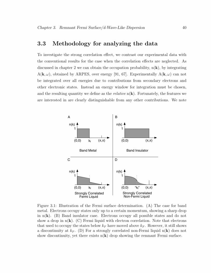
Chapter 3. Remnant Fermi Surface/d-Wave-Like Dispersion 40
3.3 Methodology for analyzing the data
To investigate the strong correlation effect, we contrast our experimental data with
the conventional results for the case when the correlation effects are neglected. As
discussed in chapter 2 we can obtain the occupation probability, n(k), by integrating
A(k, ω), obtained by ARPES, over energy [91, 67]. Experimentally A(k, ω) can not
be integrated over all energies due to contributions from secondary electrons and
other electronic states. Instead an energy window for integration must be chosen,
and the resulting quantity we define as the relative n(k). Fortunately, the features we
are interested in are clearly distinguishable from any other contributions. We note
(0,0) (π,π)
n(k)1
Band Metal Band Insulator
(0,0) (π,π)
n(k)1
Strongly Correlated Fermi Liquid
(0,0) (π,π)
n(k)1
kf
kf
A B
C D
(0,0) (π,π)
n(k)1
“kf”
Strongly Correlated Non-Fermi Liquid
Figure 3.1: Illustration of the Fermi surface determination. (A) The case for bandmetal. Electrons occupy states only up to a certain momentum, showing a sharp dropin n(k). (B) Band insulator case. Electrons occupy all possible states and do notshow a drop in n(k). (C) Fermi liquid with electron correlation. Note that electronsthat used to occupy the states below kF have moved above kF . However, it still showsa discontinuity at kF . (D) For a strongly correlated non-Fermi liquid n(k) does notshow discontinuity, yet there exists n(k) drop showing the remnant Fermi surface.

Chapter 3. Remnant Fermi Surface/d-Wave-Like Dispersion 41
that n(k) is a ground state property, and hence is different from the integration of
the single-particle spectral weight, A(k, ω), over energy. However, under the sudden
approximation integration of A(k, ω) as measured by ARPES gives n(k) [91, 67]. We
then use the drop in the relative n(k) to determine the Fermi surface as illustrated
in figure 3.1. For a metal with non-interacting electrons, the electron states are filled
up to the Fermi momentum, kF , and the n(k) shows a sudden drop(figure 3.1A).
As more electrons are added, the electron states are eventually filled and the system
becomes an insulator with no drop in n(k) (figure 3.1B). Therefore, the drop in
n(k) characterizes the Fermi surface of a metal with non-interacting electrons. When
correlation increases, n(k) begins to deform (figure 3.1C), although there is still some
discontinuity at kF when the correlation is moderate. Note that the electrons that
used to occupy states below kF have moved to the states that were unoccupied.
For a non-Fermi liquid with very strong correlation, n(k) drops smoothly without a
discontinuity(panel (D)). Several theoretical calculations using very different models
have found that n(k) of the interacting system mimics that of the non-interacting
system, even when the material is fully gapped[37, 38, 39, 92]. Hence we can recover
the remnant of a Fermi surface or an underlying Fermi surface by following the contour
of steepest descent of n(k) even when correlation is strong enough that the system
becomes a Mott insulator.2 The volume obtained by this procedure is consistent with
half-filling as expected in a Mott insulator.
We now apply this method to determine the Fermi level crossing of a real system.
The traditional way (figure 3.2A) is shown for the ARPES spectra on the (0,0) to
(π, π) cut taken from Bi2212 which is metallic. As we move from (0,0) toward (π, π),
the peak disperses to the Fermi level, EF . As the peak reaches EF and passes it, it
begins to lose spectral weight (this again is kF ). Alternatively, we simply integrate
the spectral function from 0.6 eV to -0.1 eV relative to the EF , and the resulting
relative n(k) is plotted in figure 3.2C. We can now define kF as the point of steepest
descent in the relative n(k). The same conclusion can be drawn here independent of
the method we use. Note that the n(k) also drops as we approach (0,0); this is a
2A key difference between a Mott insulator and a band insulator is that∑
k n(k)/(Brillouin zonevolume) equals 1 for a Mott insulator, and equals 2 for a band insulator.

Chapter 3. Remnant Fermi Surface/d-Wave-Like Dispersion 42
B D
1,0 1,1
rela
tive
n(k
)In
tens
ity (
arb.
uni
ts)
Binding Energy (eV)1 0
KF
0
.09
.18
.27
.36
.45
.54
.71
.89
.98
(π,yπ)
y =
C
0,0 1,0
1,1
KF
0,0 1,1
rela
tive
n(k
)
00.5
Binding Energy (eV)
Inte
nsity
(ar
b. u
nits
)
kx=ky= 0.19
.29
.33
.38
.43
.48
.57
.67
.71
.76
.86
kx=ky=
A
0,0 1,0
1,1
kF kF
KF
KF
Bi2212 La3-xSrxMn2O7
Figure 3.2: Application of the method described in figure 3.1. (A) Spectra alongthe (0,0) to (π, π) cut from Bi2212. The peak disperses towards the low energy sideand reaches the Fermi level at kF , (0.43π, 0.43π). (B) Spectra along the (π, 0) to(π, π) cut from metallic La3−xSrxMn2O7. The peak disperses toward the low energyside, but never reaches the Fermi energy. However, it loses intensity as it crosses theposition where the band calculation predicts the Fermi surface, showing an underlyingFermi surface. (C) and (D) plots of the relative n(k) for the data in (A) and (B),respectively, show a sudden drop around kF , essentially showing the two methodsgive the dame Fermi momentum kF .

Chapter 3. Remnant Fermi Surface/d-Wave-Like Dispersion 43
photoemission artifact, because the photoemission cross-section of the dx2−y2 orbital
vanishes due to symmetry.
We can show that the n(k) procedure is still valid for strongly correlated sys-
tems with gapped Fermi surface by presenting ARPES spectra on ferromagnetic
La3−xSrxMn2O7 on the (π, 0) to (π, π) cut (figure 3.2B)[93]. It shows a dispersive
feature initially moving toward EF and then pulling slightly back away from EF
around (π, 0.27π), but never reaching the EF . However, the feature suddenly loses its
spectral weight when it crosses (π, 0.27π) as if it crosses the Fermi surface as shown
in panel D. Furthermore, the Fermi surface determined by a local density approxima-
tion calculation coincides with the Fermi surface determined by the n(k) despite the
spectra of this ferromagnetic metallic state material having a significant gap. Thus,
the underlying Fermi surface can survive a strong interaction, and the n(k) method
is effective in identifying it even when the peak does not disperse across EF .
3.4 Results from an insulator
The low-energy feature along the (0,0) to (π, π) cut in Ca2CuO2Cl2 (figure 3.3A) has
the same origin as the low-energy peak seen in Bi2212, the Zhang-Rice singlet on the
CuO2 plane. As k increases from (0,0) toward (π, π), the peak moves to lower energy
and subsequently pulls back to higher energy as it crosses (π/2, π/2). Its spectral
weight increases as it moves away from the (0,0) point for the reason described earlier,
and then drops as it crosses (0.43π, 0.43π). These changes along the (0,0) to (π, π)
cut are consistent with the earlier reports on Sr2CuO2Cl2[25, 26, 54]. Similar to the
drop of n(k) across the Fermi surface seen in Bi2212, Ca2CuO2Cl2 also shows that
the intensity of the peak n(k) drops as if there is a crossing of EF even though the
material is an insulator. The intensity along the (0,0) to (π, 0) cut (figure 3.3B) goes
through a maximum around (2π/3, 0) as in Sr2CuO2Cl2. This behavior is also seen in
superconducting cuprates.[94] Earlier works on Sr2CuO2Cl2 show the spectral weight
along the (π, 0) to (π, π) cut is strongly suppressed. However, for Ca2CuO2Cl2, the
improved spectral quality allows us to clearly observe the spectral weight drop along

Chapter 3. Remnant Fermi Surface/d-Wave-Like Dispersion 44
ky=kx
0,0 1,1
kx=1
1,0 1,1
ky= 0
0,0 1,0
kx=ky= 0
kx=ky
A
01
0.19
0.29
0.38
0.43
0.48
0.57
0.81
0.90
1.000,0 1,0
1,1 E
Binding Energy Relative to the (π/2,π /2) peak position (eV)
Inte
nsity
(ar
b. u
nits
)
Rel
ativ
e n(
k) (
arb.
uni
ts)
0
C
0,0 1,0
1,1
ky= 0
0.10
0.19
0.29
0.38
0.48
0.57
0.81
ky=1
kx=1
1
B
0,0 1,0
1,1
kx=0
0.19
0.38
0.48
0.57
0.67
0.76
0.86
0.95
kx=1
ky= 0
01
ky=kx-.38
.38,0 1,.57
D
0,0 1,0
1,1
01
(.38
(.48,
(.57,
(.67,
(.76,
(1.0,
(kx,
.00)
ky)
.57)
.38)
.29)
.19)
.10)
Figure 3.3: (A) (0,0) to (π, π) cut. The peak disperses towards the low energy sideand loses intensity near the (π/2, π/2) point. (B) (0,0) to (π, 0) cut. The lowestenergy peak shows little dispersion. The spectral weight initially increases and thendecreases again after (0.67π, 0) as in the Sr2CuO2Cl2 case [26, 54]. However, notethat there is appreciable spectral weight at (π, 0) contrary to the Sr2CuO2Cl2 case.(C) (π, 0) to (π, π) cut. The spectral weight drops as we move to (π, π). (D) Anothercut (as marked in the inset) showing the n(k) drop. (E) relative n(k)s constructedfrom the spectra in panels A-D. The relative increase of spectral weight above 0 iscaused by emission from second order light. The insets and labels show where thespectra were taken in the Brillouin zone.
the (π, 0) to (π, π) cut (figure 3.3C)3. Note that the spectral weight drops as we move
toward the (π, π) point, which we attribute to the crossing of a remnant Fermi surface.
We also show another cut (figure 3.3D) which exhibits essentially the same behavior.
3As generally found in photoemission experiments, the change of photoemission cross-section foreach sample is hard to calculate quantitatively. At the qualitative level, data from Ca2CuO2Cl2 andSr2CuO2Cl2 are consistent with each other.

Chapter 3. Remnant Fermi Surface/d-Wave-Like Dispersion 45
The relative n(k)s of the cuts are summarized in figure 3.3E in arbitrary units. The
relative n(k) here and in figure 3.4 were obtained by integrating from 0.5 eV to -0.2
eV relative to the peak position at (π/2, π/2). All of the n(k)s show a drop (after
the maximum) as we cross the remnant Fermi surface. Here we emphasize that we
are using the same method as we do for metals, where the identification of a Fermi
surface is convincing.
The remnant Fermi surface can be identified in the relative n(k) contour plot of
Ca2CuO2Cl2 (figure 3.4A). The little crosses in the figure denote the k-space points
where spectra were taken. The data points here and in figure 3.4C have been reflected
about the line ky=kx to better illustrate the remnant Fermi surface. Again, it should
be emphasized that the suppressed n(k) near (0,0) comes from the vanishing photoe-
mission cross section due to the dx2−y2 orbital symmetry rather than a remnant Fermi
surface crossing. For the same reason, the photon polarization suppresses the overall
spectral weight along the (0,0) to (0, π) line as compared with the (0,0) to (π, 0) line.
In figure 3.4B we present the relative n(k) of an optimally doped Bi2212 sample in
the normal state. In this case the identification of the Fermi surface is unambiguous,
but the same matrix element effects that were seen in the insulator can be seen in the
metallic sample as well. However, for both samples, the drop in n(k) near the diago-
nal line connecting (π, 0) and (0, π) can not be explained by the photoemission cross
section. In the metallic case, the Fermi surface is clearly identified (the white-hashed
region in figure 3.4B). For the insulator, the drop is approximately where band theory
predicts the Fermi surface.[95] Therefore, we attribute the behavior in the insulator to
a remnant of the Fermi surface that existed in the metal. The similarity of the results
in the insulator and the metal makes the identification of the remnant Fermi surface
unambiguous. The white hashed area in figure 3.4A represents the area where the
remnant Fermi surface may reside as determined by the relative n(k). Although there
is some uncertainty in the detailed shape of this remnant Fermi surface, this does not
affect the discussion and the conclusions drawn below. The relative n(k) we presented
is a very robust feature. In metallic samples with partially gapped Fermi surfaces,
underlying Fermi surfaces have also been identified in the gapped region[93, 96, 97].
This effect is similar to what we report here in the insulator. The remnant Fermi

Chapter 3. Remnant Fermi Surface/d-Wave-Like Dispersion 46
20
15
10
5
0
20151050
20
15
10
5
0
20151050 π
πRelative n(k) (Arb. Units)
kyπ/2
kxπ/2
20
15
10
5
020151050 π
0
π
0
Relative n(k) (Arb. Units)
kx
kyπ/2
π/2
A B
300
200
100
0
Hig
h E
nerg
y ‘G
ap’
(mev
)
1 .00.80.60.40.20.0
|cos(kxa) - cos(kya)| /2
(0,0) (π,0)
(π,π)
π
0
π0
Peak Position(k)
kx
ky
-350 meV
0 meV
π/2
π/2
CD
Figure 3.4: Contour plot of the relative n(k). (A) n(k) from the spectra shown infigure 3.3. The color scale on the right represent n(k). The spectra were taken onlyin the first octant of the first Brillouin zone (crosses). The n(k) plot was folded tobetter represent the remnant Fermi surface. Note, the n(k) drops as we cross theapproximate diagonal line connecting (0, π) and (π, 0). The hashed area representsapproximately where the remnant Fermi surface exists. (B) An identical plot for anoptimally doped Bi2212 sample in the normal state. (C) Contour plot of the lowestenergy peak position from the spectra in figure 3.3 relative to the (π/2, π/2) peak.The hashed area is from (A), showing the remnant Fermi surface. The color scaleon the right indicates the relative binding energy of the peak. (D) The ’gap’ versus| cos kxa − cos kya|. The straight line shows the d-wave line. The inset is a moreillustrative figure of the same data as explained in the text.

Chapter 3. Remnant Fermi Surface/d-Wave-Like Dispersion 47
surface in the underdoped Bi2212 was also identified at similar locations to the n(k)
drop in these materials with a different criteria of minimum gap locus[96, 97]. Cal-
culations also show the Fermi surface defined by n(k) is robust in the presence of
strong correlation[37, 38, 92]. Given that there is a remnant Fermi surface as shown
by the white hashed lines in figure 3.4, A and C, the observed energy dispersion along
this line has to stem from the strong electron correlation. In other words, the elec-
tron correlation disperses the otherwise iso-energetic contour of the remnant Fermi
surface. This dispersion is consistent with the non-trivial d-wave | cos kxa − cos kya|form[84, 85, 86, 87, 44]. These results also support our identification of the remnant
Fermi surface in a Mott insulator.
Figure 3.4C plots the energy contour of the peak position of the lowest energy
feature of Ca2CuO2Cl2 referenced to the energy of (π/2, π/2) peak. The hashed area
indicates the remnant Fermi surface determined in figure 3.4A. The ’Fermi surface’ is
no longer a constant energy contour as it would be in the non-interacting case. Instead
it disperses as much as the total dispersion width of the system. In figure 3.4D we
plot the dispersion at different points on the remnant Fermi surface referenced to the
lowest energy state at (π/2, π/2). The dispersion of the peaks along the Fermi surface
is plotted against | cos kxa − cos kya|. The straight line shows the d-wave dispersion
function at the ’Fermi surface’ with a d-wave energy gap. The figure in the inset
presents the same data in a more illustrative fashion. On a line drawn from the center
of the Brillouin zone to any point either experimental (blue) or theoretical (red), the
distance from this point to the intersection of the line with the antiferromagnetic
Brillouin zone boundary gives the value of the ’gap’ at the k-point of interest. The
red line is for a d-wave dispersion along (π, 0) to (0, π). The good agreement4 is
achieved without the need for free parameters. This d-wave like dispersion can only
be attributed to the many-body effect. The relative energy difference between the
energy at (π/2, π/2) and (π, 0) has been referred to as a gap[44], which we follow.
This gap differs from the usual optical Mott gap (figure 3.5) and may correspond
to the momentum dependent gap once the system is doped. This gap monotonically
4The details on whether or not the dispersion near the d-wave node is a cusp is addressed inchapter 5. The motivation to compare the data with the d-wave function stems from the fact thatthe insulator is related to a d-wave superconductor (and thus a d-wave gap) by doping.

Chapter 3. Remnant Fermi Surface/d-Wave-Like Dispersion 48
Mott Gap
-400
-300
-200
-100
0
En
erg
y R
elat
ive
to V
alen
ce B
and
Max
imu
m (
meV
)
Quasi-particle Dispersion
Ca2CuO2Cl2
Bin
din
g E
ner
gy
(meV
)
00
-ππ
π-π
kxky
Fermi Surface Remnant
n(k)
00
-ππ
π-π
kxky
Fermi Surface
n(k)
Bi2212A B
d-wave gap
d-waveLike ‘Gap’
-400
-300
-200
-100
0
Quasi-particle Dispersion
EF
Figure 3.5: An illustration showing the two experimental features presented in thischapter on the insulator, and the similarity they show to a slightly overdoped Bi2212sample. (A) The bottom half shows the relative n(k), and above it lies the approxi-mate remnant Fermi surface derived from it. However, there is much dispersion overthe entire Brillouin zone, and the remnant Fermi surface is no longer an iso-energeticcontour as can be seen by the quasiparticle dispersion (energy relative to the valenceband maximum). Here the remnant Fermi surface is shown as a black and white linerunning over the visible portions of the dispersion contour. For clarity, a portion ofthe dispersion along the remnant Fermi surface is shown in the top half. Note theidea presented that the isoenergetic contour(dashed black line) is deformed by strongcorrelation to the observed red curve. The d-wave like ’gap’ referred to in the textis the quasiparticle energy deviation from the dashed black line set at the energy ofthe (π/2, π/2) point. The difference between this ’gap’ and the Mott gap can now beseen clearly. (B) For overdoped Bi2212, n(k) defines the actual Fermi surface. Thequasiparticle dispersion (binding energy) shows states filled to an isoenergetic Fermisurface. In the top panel one is reminded that below Tc, a d-wave superconductinggap opens. This is an intriguing similarity between the insulator and the metal.

Chapter 3. Remnant Fermi Surface/d-Wave-Like Dispersion 49
increases when we move away from (π/2, π/2) as also reported earlier[25]. As well
as summarizing the data presented, figure 3.5 also shows the intriguing similarity
between the data from the insulator and a slightly overdoped d-wave superconduc-
tor(Bi2212), and thus gives the reason for comparing the dispersion along the remnant
Fermi surface with the | cos kxa − cos kya| form. In the superconducting case, n(k)
helps determine the Fermi surface. The anisotropic gapping of this surface below
Tc reveals the d-wave nature of the gap. In the insulator, n(k) helps determine the
remnant Fermi surface. The k-dependent modulation along this surface reveals the
d-wave like dispersion. Whether this similarity between the insulator and the doped
superconductor is a reflection of some underlying symmetry principle is a question
which needs to be investigated [98, 99].
The above analysis is possible only because we now observe the remnant Fermi
surface. Although the dispersion for Sr2CuO2Cl2 was similar to the present case, the
earlier results did not address the issue of a remnant Fermi surface because the smaller
photoemission cross section along the (π, 0) to (π, π) cut prevented this identification.
Therefore the analysis shown above was not possible. With only the energy contour
information (such as in Fig 4C), it is plausible to think that the Fermi surface evolves
to a small circle around the (π/2, π/2) point.[100] However, with the favorable pho-
toemission cross section, the results from Ca2CuO2Cl2 show that the Fermi surface
leaves a clear remnant, although it may be broadened and weakened. Therefore, the
energy dispersion along the original Fermi surface of a non-interacting system is due
to the opening of an anisotropic ’gap’ along the same remnant Fermi surface.
The same analysis is shown in figure 3.6 for Bi2212 with different Dy dopings
together with Ca2CuO2Cl2 results. The corresponding doping level and Tc as a func-
tion of Dy concentration are also shown. The energy for Ca2CuO2Cl2 is referenced
to the peak position at (π/2, π/2) and that for Dy doped Bi2212 is to EF . However,
the two energies essentially refer to the same energy since the peak on the (0,0) to
(π, π) cut for all Bi2212 samples reaches the Fermi level. Note that the gaps for Dy
doped Bi2212 data also follow a function that is qualitatively similar to the d-wave
function with reduced gap sizes as shown with the (π, 0) spectra in figure 3.6B. This
result suggests that the d-wave gap originating in the insulator continuously evolves

Chapter 3. Remnant Fermi Surface/d-Wave-Like Dispersion 50
B
A
0.0 0.5 1.00
100
200
300
400H
igh
Ene
rgy
Gap
(meV
)
|cos(kxa) - cos(kya)| /2
10% Dy Tc=65K17.5% Dy Tc=25K35% Dy Tc=0KCa2CuO2Cl2
-1.0 -0.8 -0.6 -0.4 -0.2 0.0 0.2
Ca2CuO2Cl2 (insulator)
Tc=0K
Tc=25K
Tc=65K
Tc=85K
Inte
nsity
(arb
itrar
yun
it)
Energy relative to EF or peak at (π/2,π/2) (ev)
Figure 3.6: (A) Combined d-wave plot of the data from Ca2CuO2Cl2 and Bi2212with various Dy dopings. (B) The spectra at (π, 0), showing the evolution of the highenergy pseudo gap as a function of doping, as previously stressed by Laughlin[44].

Chapter 3. Remnant Fermi Surface/d-Wave-Like Dispersion 51
with doping, but retains its anisotropy as a function of momentum and that the high
energy pseudo gap in the underdoped regime is the same gap as the d-wave gap seen
in the insulator as discussed above. Of course, the high energy pseudo gap in the
underdoped regime is smaller than the gap in the insulator. In a sense, the doped
regime is a diluted version of the insulator, with the gap getting smaller with increas-
ing doping. The two extremes of this evolution are illustrated in the quasiparticle
dispersions shown in figure 3.5. The insulator shows a large d-wave like dispersion
along the remnant Fermi surface. In the overdoped case, no gap is seen in the normal
state along an almost identical curve in k-space; however, a d-wave gap is observed
in the superconducting state. Although their sizes vary, the d-wave superconducting
gap, and the d-wave ’gap’ of the insulator have the same non-trivial form, and are
thus likely to stem from the same underlying mechanism.
3.5 Implications of a remnant Fermi surface in a
Mott insulator
We do not know the full implications of the data we report, but can offer the following
possibilities. First, we compare the experimental dispersion with a simple spin-density
wave picture. Starting with the Hubbard model
H =∑σk
εkc†kσckσ + U
∑i
ni↑ni↓ (3.1)
with
εk = −2t(cos(kxa) + cos(kya)) − 4t′(cos(kxa)cos(kya))−
2t′′(cos(2kxa) + cos(2kya)) (3.2)
and adding a SDW picture, the following dispersion relation will be found
Chapter 3. Remnant Fermi Surface/d-Wave-Like Dispersion 52
Ek± ≈ −4t′(cos(kxa)cos(kya)) − 2t′′(cos(2kxa) + cos(2kya))
±[U/2 + J(cos(kxa) + cos(kya))2] (3.3)
with J = t2/U . With realistic values for t′ and t′′, and an experimental value for
J of -0.12 eV, 0.08 eV, and 0.125 eV respectively,[26] we find that the experimental
dispersion deviates significantly from this mean field result giving a bandwidth of
1.1 eV. It is crucial to note the observed isotropic dispersion around the (π/2, π/2)
point, with almost identical dispersions from (π/2, π/2) to (0,0) and from (π/2, π/2)
to (π, 0). This result is unlikely to be a coincidence of the parameters t′, t′′, and J as
suggested by the SDW picture above.
We now compare the data with numerical calculations that, unlike the mean
field SDW picture, appropriately accounts for the dynamics. Being mainly con-
cerned with the dispersion relation, we concentrate our discussion on the t-J model as
more extensive literature exists and as J can be independently measured.[38] Quali-
tatively, the same conclusion is expected for the Hubbard model[101], which has the
added advantage of yielding n(k), but has more uncertainty in the parameter U . Al-
though the t-J model correctly predicts [38] the dispersion along (0,0) to (π/2, π/2)
quantitatively[25], with the band width along this direction solely determined by J, it
incorrectly predicts the energy of (π, 0) to be nearly degenerate to (π/2, π/2). This is a
serious deficiency of the t-J model, because the evolution of the (π, 0) feature is crucial
to understand the d-wave-like pseudo gap. The inclusion of the next nearest neighbor
hoppings of t′ and t′′ can resolve this problem [101, 32, 102, 29, 103, 27, 104, 28, 33, 31].
In fact, the t-t′-t′′-J model can account for both the dispersion and lineshape evolu-
tion over all doping levels, which is a remarkable success of this model.[26, 32] With
a J/t ratio in the realistic range of 0.2 to 0.6, the t-t′-t′′-J model shows that the
dispersion from (π/2, π/2) to (0,0) and to (π, 0) are equal and scaled by J .[105, 106]
This result supports the notion that the isotropic dispersion is controlled by a single
parameter, J , as stressed by Laughlin.[44]
The above discussion indicates that we have a model, when solved by Monte
Carlo or exact diagonalization, that can account for the data, but what does the

Chapter 3. Remnant Fermi Surface/d-Wave-Like Dispersion 53
data fitting the non-trivial | cos kxa − cos kya| function so well mean? As pointed
out [26], the key to the inclusion of t′ and t′′ is that the additional hole mobility
destabilizes the one-hole Neel state with the hole at (π, 0) and makes the system with
one-hole move closer to a spin liquid state rather than to a Neel state that is stable
in the t-J model. This point is relevant to some early literature of the resonating
valence bond(RVB) state[18, 107]. Anderson conjectured that the ground state of
the insulator at half filling is a RVB spin liquid state.[18] This idea was extended in
the context of a mean field approach to the t-J model that yields a d-wave RVB or
flux phase solution.[84, 85, 86] The mean-field solution also predicts a phase diagram
similar to what is now known about the cuprates, with the d-wave like spin gap in
the underdoped regime being the most successful example. The problem with the
mean-field solution of the t-J model is that it does not agree with exact numerical
calculation results[38], and the half-filled state was found by neutron scattering to
have long range order[108, 109]. If these numerical calculations are right then the
d-wave RVB is not the right solution of the t-J model. However, the d-wave RVB
like state may still be a reasonable way to think about the experimental data that
describes the situation of the spin state near a hole[110]. It is just that one has to
start with a model where the single hole Neel state is destabilized, as in the t-t′-t′′-J
model. We leave this open question as a challenge to theory.
The presence of d-wave like dispersion along the remnant Fermi surface shows that
the high energy pseudo gap is a remnant of the d-wave ’gap’ seen in the insulator.
The details of the evolution of this gap, and its connection to the low energy pseudo
gap (which is likely due to pairing fluctuations) as well as the superconducting gap is
unclear at the moment. However, we believe that there has to be a connection between
these gaps of the similar | cos kxa− cos kya| form, as their presence is correlated with
each other[74].

Chapter 4
Universality of the Electronic
Structure from a Half Filled CuO2
Plane
4.1 Introduction
One approach to unraveling the mysteries of the High Tc superconductors is to under-
stand how the electronic structure evolves from an antiferromagnetic insulator to a su-
perconductor upon doping. La2−xSrxCuO4(LSCO) is the one system which has been
successfully grown from half filling to heavily overdoped; however, Angle Resolved
Photoemission (ARPES) results on these crystals remain somewhat controversial due
to the poor surface quality obtained in the experiments. YBa2Cu3O6+δ(YBCO),
which can cover the range of half-filling to optimal doping, might appear as the next
suitable candidate, but the presence of a surface state and the existence of one di-
mensional chains has clouded the interpretation of its bulk electronic structure. In
this regard, the Bi2Sr2CaCu2O8+δ(Bi2212) system, with its extremely good cleavage
plane, has been ideal for ARPES. For precisely this reason, the majority of ARPES
data on the High Tc’s to date have come from Bi2212. Unfortunately, high quality
Bi2212 crystals at very low dopings have not been achieved. On the other hand,
A2CuO2Cl2 (A=Sr,Ca) also cleaves extremely well and gives high quality ARPES
54

Chapter 4. Electronic Structure of a CuO2 plane 55
data comparable to that seen in optimally doped Bi2212, but in this case, single crys-
tals have only been available at half filling. As a result there exists no single system
to study the electronic structure from the antiferromagnetic insulator to the heavily
over doped metal.1
The solution to this problem has been to make the reasonable assumption, that
the low energy physics of the Bi2212 and A2CuO2Cl2(ACOC) systems are identi-
cal due to the fact that the CuO2 planes are common to both structures. Thus
the entire doping range can be studied. However, these two systems also have sev-
eral differences. Bi2212 is a bilayer system compared with the single CuO2 plane
per unit cell of ACOC. (Although the single layer compound Bi2Sr2CuO6+δ(Bi2201)
can also be studied, but has similar problems to Bi2212.) Sr2CuO2Cl2(SCOC) and
Ca2CuO2Cl2(CCOC) have a Cu-O-Cu distance of 3.97A and 3.87A respectively[49],
compared to 3.83A for Bi2212 [111], and they also do not possess any orthorhombic
distortion or superstructure effects which plague Bi2212. Finally, the most striking
difference in ACOC is that the apical oxygen has been replaced with a halide atom,
in this case chlorine. Given these differences, it is important to test whether or not
they can have an effect on the low energy electronic structure.
In this chapter I will justify the assumption that low energy ARPES data on
the oxychlorides are representative of photoemission from a generic, half-filled CuO2
plane, and thus may be reasonably compared with ARPES data on hole doped Bi2212.
This will be done by showing that replacing the apical chlorine with bromine has no
effect on the low energy electronic structure. Furthermore, it will also be shown that
heavily underdoped Bi2212, near half filling, despite having relatively poor spectral
quality is qualitatively consistent with the results on the oxyhalides. Finally, ARPES
on Sr2Cu3O4Cl2, which contains an additional copper atom in every other CuO2
plaquette, demonstrates that the Zhang-Rice singlet is surprisingly unaffected by
even a seemingly large modification of the CuO2 plane.
1Recently, hole doped Ca2−xNaxCuO2Cl2 single crystals have been grown[56]. ARPES resultson these crystals will be presented in chapter 6.

Chapter 4. Electronic Structure of a CuO2 plane 56
4.2 Experimental
A2CuO2X2 (A=Sr, Ca; X=Cl, Br) and Bi2Sr2MCu2O8 (M=Er, Dy) single crystals
were grown by a flux method described elsewhere.[88, 112] ARPES experiments were
performed at beamlines V-3 and V-4 of SSRL. Crystals were oriented prior to the
experiment by Laue back reflection, and cleaved in situ at a base pressure better than
5 x 10⁻¹¹ torr. The energy and angular resolution was ≤70meV and ±1◦, respectively.
The measurement temperature differs between samples to account for charging issues,
and the photon flux was then varied to determine whether or not the sample was
charging. Slight charging was in fact observed for the presented Ca2CuO2Br2 and
Sr2Cu3O4Cl2 samples, but the results were reproducible and the spectra simply shifted
to higher binding energy with increased flux indicating a uniform potential barrier
due to charging.
4.3 Sr2CuO2Cl2 and Ca2CuO2Cl2
Figure 4.1 presents a comparison between SCOC and CCOC along the high symmetry
directions. The two are almost identical. This is to be expected as Sr and Ca are
isovalent and lie in the charge reservoir layer. Along (0,0) to (π, π) both show a
feature which emerges from the background, disperses towards the chemical potential,
reaches a maximum at (π/2, π/2) and then loses weight rapidly as it pushes back to
higher binding energy. We note that the centroid of the feature at (π/2, π/2) still lies
well below the chemical potential, indicative of the fact that these crystals are Mott
insulators. The precise value ranges from 0.3eV to 1.8eV depending on where the
chemical potential has been pinned for a particular cleave of the insulator. Along the
(0,0) to (π, 0) cut a more intense and significantly more asymmetric peak is observed.
Under certain experimental conditions it becomes clear that this strong asymmetry
is due to the presence of a second feature which lies approximately 600meV below
the main band.[26] The dispersion of this second feature appears similar to that of
the lower binding energy feature, although the intensity is not. The features along
the (π, 0) cuts do not show much dispersion, and lie approximately 300meV below

Chapter 4. Electronic Structure of a CuO2 plane 57
75
6758504233170%
83
Γ Γ
83
67
50
33
17
0%
100
1.0 0.5 0.0
7567
58
50
4233170%
Γ (π,0)
(π,π)
1.0 0.5 0.0
(0,0)
(π,0)
(π, π)(0,0)
1.0 0.5 0.0 1.0 0.5 0.0
(π,0)
(2π/3,0)
(π/2, π/2)
48
10
202938
0%
57
1.0 0.5 0.0 1.0 0.5 0.0
(0,0)
(π,0)
(0,0)
1.0 0.5 0.0 1.0 0.5 0.0
(π,0)
(π/2, π/2)
0%2 02 93 8
4 8
5 7
8 1
9 0100
0%3 84 85 76 77 6
8 6
9 5
100
100
81
350 meV
350 meV
(π,0)
(π,π)
(π,0)
(π,π)
Γ ΓΓ (π,0)
(π,π)
(π,0)
(π,π)
(π,0)
(π,π)
Binding Energy Relative to the Valence Band Maximum (eV)
Binding Energy Relative to the Valence Band Maximum (eV)
Inte
nsity
(A
rb.
units
)In
tens
ity (
Arb
. un
its)
a)
b)
(π, π)(π, π)
(π, π)
Figure 4.1: EDCs of Sr2CuO2Cl2(a) and Ca2CuO2Cl2(b) along the high symmetrydirection indicated in the insets. The final panel indicates the magnitude of the d-wave-like dispersion seen in the oxyhalides, and the difference in lineshape exhibitedas a function of k. The measurement conditions were T=150K, Eγ=22.4eV andT=100K, Eγ=25.2eV for Sr2CuO2Cl2 and Ca2CuO2Cl2, respectively.

Chapter 4. Electronic Structure of a CuO2 plane 58
the maximum in dispersion at (π/2, π/2). The one significant difference between
SCOC and CCOC is the observed spectral weight at (π, 0) in CCOC which is absent
in SCOC. On going from (π, 0) to (π, π) it can be seen that this weight vanishes
quickly. Although it is not clear why the matrix elements would favor CCOC over
SCOC in the (π, 0) region, it is this difference which facilitated the identification of
a remnant Fermi surface in CCOC which was not observed in previous studies on
SCOC. One of the most significant features of the insulator is the dispersion between
(π/2, π/2) and (π, 0). The right panels makes a clear illustration of this. There are
two aspects to notice here. The most important of which is clearly the difference of
roughly 350meV in dispersion. This is the magnitude of the d-wave-like modulation
seen in the insulator. The second is the strong difference in lineshape. At (π/2, π/2)
the spectra show a clear peak which resembles a quasiparticle like peak, albeit with
a very large width, while at (π, 0), the spectra merges more continuously into the
high energy background, somewhat resembling a step function. These will be the
benchmarks to which the other compounds will be compared in determining whether
or not the data from SCOC and CCOC are representative of a single CuO2 plane.
4.4 Ca2CuO2Br2
The biggest difference between ACOC and other high Tc cuprates is the presence of
chlorine as opposed to oxygen in the apical site. To see whether or not the apical
site has an effect on the electronic structure we present in figure 4.2 ARPES data
from Ca2CuO2Br2 where bromine has replaced chlorine in the apical site. On the cut
from (0,0) to (π, π) a dispersive feature is clearly observed with a minimum in binding
energy at (π/2, π/2) and an overall bandwidth of approximately 300 meV. In panel (b)
the spectra at (π/2, π/2) and (π, 0) are compared. This data looks almost identical
to CCOC which was shown in figure 4.1. Specifically, the lineshape at (π/2, π/2) is
quite sharp and well defined compared with the broad feature seen at (π, 0). The
energy difference of 270 meV is also consistent with that seen in CCOC. We also took
a limited amount of data on Sr2CuO2Br2. The general features were consistent with
that of the other oxyhalides, although significant charging was observed. The data

Chapter 4. Electronic Structure of a CuO2 plane 59
12.011.511.010.510.0 12.011.511.010.510.0
Kinetic Energy (eV)
Inte
nsity
(A
rb. U
nits
)
270 meV(0,0)
(π,0)
(π,π)
(0,π)
(π,0)
(π/2,π/2)
(0,0)
(π,π)
Figure 4.2: a) EDCs of Ca2CuO2Br2 from (0,0) to (π, π) taken with 16.5eV photonsat T=372K. b) Comparison of (π/2, π/2) and (π, 0).
on the oxybromides is strong evidence that the low energy excitations are relatively
independent of the apical atoms and the observed spectral function in ACOC thus
originates from the half filled CuO2 plane. Consequently, the comparison of ARPES
data on ACOC at x=0 with Bi2212 data at finite doping is valid.

Chapter 4. Electronic Structure of a CuO2 plane 60
4.5 Bi2Sr2ErCu2O8 and Bi2Sr2DyCu2O8
Of course the ideal scenario to examine the doping evolution is to study the same
system through the entire doping range. Therefore, we also present Er and Dy doped
Bi2212 crystals grown near half filling. Figure 4.3 shows the valence band of Er doped
Bi2212 at (0.63π, 0) and (0, 0.63π). The valence band spectra are comparable to those
of Bi2212 at various other dopings[113]. The spectra have been normalized only by
the incident flux, and one clearly sees that the low energy spectral weight within
1.5eV of EF is suppressed in the (0, 0.63π) spectra relative to the (0.63π, 0) spectra.
As these two locations are at equivalent points in the CuO2 Brillouin zone, one can
conclude that the wave function at (0.63π, 0) is symmetric with respect to a mirror
plane parallel to the Cu-O bond direction. [For a more complete description of such
an analysis, see chapter 2.] This is consistent with results on the oxychlorides and
Bi2212[114, 113], and is the expected result for a wavefunction with dx2−y2 symmetry.
Inte
nsity
(A
rb. U
nits
)
181614121086
Kinetic Energy (eV)
(0,0) (π,0)
(0,π) (π,π)
E
(0,0.63π) (0.63π,0)
Figure 4.3: Valence band spectra of Bi2Sr2ErCu2O8 at equivalent k points (0.63π, 0)and (0, 0.63π). The inplane polarization is indicated in the figure. Eγ=22.4eV andT=230K.

Chapter 4. Electronic Structure of a CuO2 plane 61
The lack of a complete suppression at (0, 0.63π) may be due to a combination of
superstructure effects, a non zero out of plane component of the vector field, and
hybridization with alternative symmetry states.
Figures 4.4 and 4.5 show the EDCs for these samples along the high symmetry
directions. The low energy features are not nearly as well defined as in the oxyhalides;
-1.0
-0.8
-0.6
-0.4
-0.2
0.0
Bin
ding
Ene
rgy
(eV
)
-1.5 -1.0 -0.5 0
Inte
nsity
(A
rb. U
nits
)
-1.5 -1.0 -0.5 0 -1.5 -1.0 -0.5 0-1.5 -1.0 -0.5 0Binding Energy (eV)
(0,0)
(π,π) (π,0)
(0,0)
(π,π)
(π,0) (π,0)
(π/2,π/2)
(0,0)(π,π) (π,π)(π,0) (π,0) (π/2,π/2)
(0,0) (π,0)
(π,π)
(0,0) (π,0)
(π,π)
(0,0) (π,0)
(π,π)
(0,0) (π,0)
(π,π)
Figure 4.4: EDCs of Bi2Sr2ErCu2O8 along the high symmetry directions as indicatedin the cartoons. Below is a plot of the second derivative of the above EDCs, fromwhich one can trace out the dispersion. Eγ=22.4eV and T=100K.

Chapter 4. Electronic Structure of a CuO2 plane 62
-1.0
-0.8
-0.6
-0.4
-0.2
0.0
Bin
ding
Ene
rgy
(eV
)
-1.5 -1.0 -0.5 0-1.5 -1.0 -0.5 0
Binding Energy (eV)
-1.5 -1.0 -0.5 0
(0,0) (π,0)
(π,π)
(0,0) (π,0)
(π,π)
(0.6π,0.6π) (0,0) (π,0)
(0,0) (π,0)
(π,π)
0 %
27
36
45
53
62
0 %
27
54
67
81
(π,0)
118
(π/2,π/2)
(π,0)
220 meV
Inte
nsity
(A
rb. U
nits
)
Figure 4.5: EDCs of Bi2Sr2DyCu2O8 along the high symmetry directions as indicatedin the cartoons. Below is a plot of the second derivative of the above EDCs, fromwhich one can trace out the dispersion. Eγ=22.4eV and T=75K.
however, a clear shoulder does emerge from the background. The poor definition of
these features is consistent with previous studies on underdoped Bi2212 which show
that the low energy excitation spectra become smeared out as one proceeds toward
half filling.[71, 113] In fact, this is precisely the reason why ARPES data on the
oxychlorides has been so valuable to the study of high Tc superconductivity. The
reason for the relatively poor spectral quality of heavily underdoped Bi2212 is an
open question, although it is possibly simply an issue of sample quality.
Chapter 4. Electronic Structure of a CuO2 plane 63
Examining the low energy spectra from (0,0) to (π, π) of Er doped Bi2212 we see
that the shoulder is most pronounced at (π/2, π/2) with a minimum binding energy
of -0.27 eV. From (0,0) to (π, 0) the shoulder develops at higher binding energy with
a value of -0.49 eV at (π, 0) and then disappears again as one travels from (π, 0) to
(π, π). Although there is significant ambiguity in identifying the binding energy of
these features, the fact that the shoulder has a dispersion of roughly 0.22eV between
(π, 0) and (π/2, π/2) can be clearly seen in the final panel. Another way to attempt
to systematically track the dispersion is with the use of a second derivative plot also
shown in figure 4.4. One will notice that the dispersion found with this method
reproduces the above description. Results on Dy doped Bi2212 shown in figure 4.5
clearly mimic the behavior seen in the Er doped Bi2212 including the 0.22eV difference
in energy between (π/2, π/2) and (π, 0). The overall features of the dispersion and
the resulting energy difference of roughly 220 meV between (π/2, π/2) and (π, 0)
in Er and Dy doped Bi2212 is qualitatively consistent with the dispersion and the
350 meV d-wave-like modulation seen in CCOC. Thus, despite the poor definition,
the electronic structure is still qualitatively consistent between the oxyhalide and
Bi2212 systems. This result along with our data on CCOB justifies the long standing
assumption that the ARPES data from SCOC and CCOC are representative of a half
filled CuO2 square lattice.
4.6 Sr2Cu3O4Cl2: Cu3O4 plane
Sr2Cu3O4Cl2 is a particularly remarkable example of the apparent robustness of the
Zhang-Rice singlet. This system deviates from the other cuprates due to an additional
Cu atom located in every other CuO2 plaquette resulting in an in-plane stoichiom-
etry of Cu3O4. The resulting crystal structure has a unit cell twice as large as in
Sr2CuO2Cl2 and rotated by 45 degrees (see figure 4.6). Thus (π, 0) of the CuO2 unit
cell is now equivalent to (π, π) in the Cu3O4 system, and similarly (π/2, π/2) for
Sr2CuO2Cl2 is equivalent to (π, 0) for Sr2Cu3O4Cl2. However, instead of presenting
results in the new Cu3O4 basis, we will continue to present all momentum values in
the original CuO2 basis. This will make for a simpler comparison between the two

Chapter 4. Electronic Structure of a CuO2 plane 64
CuA
CuB
O
aπ/a kx
ky
CuO2 Brillouin Zone
Cu3O4 Brillouin Zone
π/aa) b)
Figure 4.6: Real space(a) and Reciprocal space(b) cartoons of the unit cell ofCu3O4(dashed line). The unit cell of the CuO2(solid line) is shown for comparison.
systems.
Sample valence band spectra at four high symmetry points of Sr2Cu3O4Cl2 are
shown in figure 4.7. Note the strong momentum dependence of the features. In
fact these spectra are quite similar to the valence band of Sr2CuO2Cl2 [114]. We
will however, continue to focus on the low energy excitations contained in the “foot”
of the valence band and expanded in the following panel for clarity. Note that the
spectra at (+π/2,−π/2) shows a clear suppression of weight with respect to the
equivalent Brillouin zone location of (+π/2, +π/2). As the polarization of the incident
light is horizontal, this suppression of spectral weight at (+π/2,−π/2) relative to
(+π/2, +π/2) indicates that the wave function at (π/2, π/2) is odd with respect to a
mirror plane at 45◦ to the Cu-O bond direction. As would be expected for a Zhang-
Rice singlet state, this observation is consistent with a dx2−y2 orbital character.
In figure 4.8, two perpendicular cuts through (π/2, π/2) are shown. Note that the
lowest energy feature is most well defined near (π/2, π/2), the dispersion is isotropic
about its minimum at (π/2, π/2), and as can be seen in the final panel, (π, 0) lies ap-
proximately 320 meV below (π/2, π/2). From the image plot normalized at high bind-
ing energy along the antiferromagnetic zone boundary one can observe that the lowest
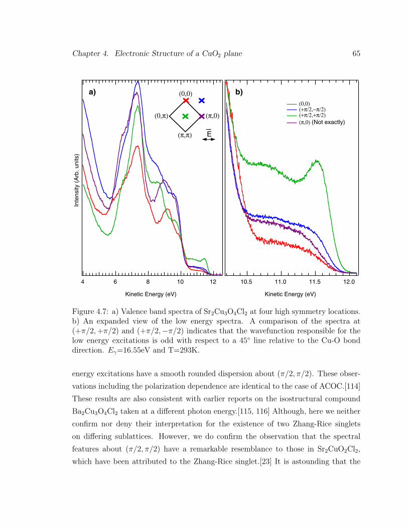
Chapter 4. Electronic Structure of a CuO2 plane 65
Inte
nsity
(A
rb. u
nits
)
1210864
Kinetic Energy (eV)
12.011.511.010.5
Kinetic Energy (eV)
(0,0) (+π/2,−π/2) (+π/2,+π/2) (π,0) (Not exactly)
E
(0,0)
(π,π)
(π,0)(0,π)
a) b)
Figure 4.7: a) Valence band spectra of Sr2Cu3O4Cl2 at four high symmetry locations.b) An expanded view of the low energy spectra. A comparison of the spectra at(+π/2, +π/2) and (+π/2,−π/2) indicates that the wavefunction responsible for thelow energy excitations is odd with respect to a 45◦ line relative to the Cu-O bonddirection. Eγ=16.55eV and T=293K.
energy excitations have a smooth rounded dispersion about (π/2, π/2). These obser-
vations including the polarization dependence are identical to the case of ACOC.[114]
These results are also consistent with earlier reports on the isostructural compound
Ba2Cu3O4Cl2 taken at a different photon energy.[115, 116] Although, here we neither
confirm nor deny their interpretation for the existence of two Zhang-Rice singlets
on differing sublattices. However, we do confirm the observation that the spectral
features about (π/2, π/2) have a remarkable resemblance to those in Sr2CuO2Cl2,
which have been attributed to the Zhang-Rice singlet.[23] It is astounding that the
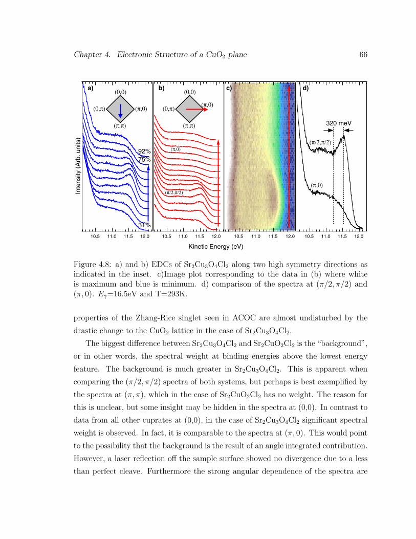
Chapter 4. Electronic Structure of a CuO2 plane 66
Inte
nsity
(A
rb. u
nits
)
12.011.511.010.5 12.011.511.010.512.011.511.010.5 12.011.511.010.5
320 meV
(0,0)
(π,π)
(π,0)(0,π) (0,π)
(0,0)
(π,0)
(π,π)
(π/2,π/2)
(π,0)(π/2,π/2)
(π,0)
31%
75%92%
Kinetic Energy (eV)
a) b) c) d)
Figure 4.8: a) and b) EDCs of Sr2Cu3O4Cl2 along two high symmetry directions asindicated in the inset. c)Image plot corresponding to the data in (b) where whiteis maximum and blue is minimum. d) comparison of the spectra at (π/2, π/2) and(π, 0). Eγ=16.5eV and T=293K.
properties of the Zhang-Rice singlet seen in ACOC are almost undisturbed by the
drastic change to the CuO2 lattice in the case of Sr2Cu3O4Cl2.
The biggest difference between Sr2Cu3O4Cl2 and Sr2CuO2Cl2 is the “background”,
or in other words, the spectral weight at binding energies above the lowest energy
feature. The background is much greater in Sr2Cu3O4Cl2. This is apparent when
comparing the (π/2, π/2) spectra of both systems, but perhaps is best exemplified by
the spectra at (π, π), which in the case of Sr2CuO2Cl2 has no weight. The reason for
this is unclear, but some insight may be hidden in the spectra at (0,0). In contrast to
data from all other cuprates at (0,0), in the case of Sr2Cu3O4Cl2 significant spectral
weight is observed. In fact, it is comparable to the spectra at (π, 0). This would point
to the possibility that the background is the result of an angle integrated contribution.
However, a laser reflection off the sample surface showed no divergence due to a less
than perfect cleave. Furthermore the strong angular dependence of the spectra are
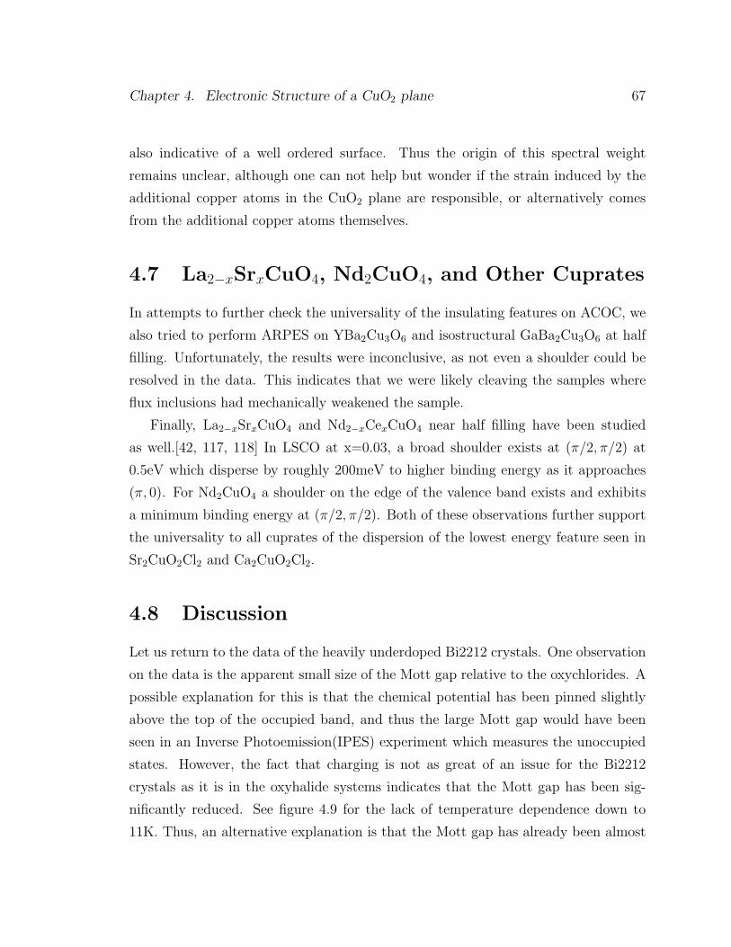
Chapter 4. Electronic Structure of a CuO2 plane 67
also indicative of a well ordered surface. Thus the origin of this spectral weight
remains unclear, although one can not help but wonder if the strain induced by the
additional copper atoms in the CuO2 plane are responsible, or alternatively comes
from the additional copper atoms themselves.
4.7 La2−xSrxCuO4, Nd2CuO4, and Other Cuprates
In attempts to further check the universality of the insulating features on ACOC, we
also tried to perform ARPES on YBa2Cu3O6 and isostructural GaBa2Cu3O6 at half
filling. Unfortunately, the results were inconclusive, as not even a shoulder could be
resolved in the data. This indicates that we were likely cleaving the samples where
flux inclusions had mechanically weakened the sample.
Finally, La2−xSrxCuO4 and Nd2−xCexCuO4 near half filling have been studied
as well.[42, 117, 118] In LSCO at x=0.03, a broad shoulder exists at (π/2, π/2) at
0.5eV which disperse by roughly 200meV to higher binding energy as it approaches
(π, 0). For Nd2CuO4 a shoulder on the edge of the valence band exists and exhibits
a minimum binding energy at (π/2, π/2). Both of these observations further support
the universality to all cuprates of the dispersion of the lowest energy feature seen in
Sr2CuO2Cl2 and Ca2CuO2Cl2.
4.8 Discussion
Let us return to the data of the heavily underdoped Bi2212 crystals. One observation
on the data is the apparent small size of the Mott gap relative to the oxychlorides. A
possible explanation for this is that the chemical potential has been pinned slightly
above the top of the occupied band, and thus the large Mott gap would have been
seen in an Inverse Photoemission(IPES) experiment which measures the unoccupied
states. However, the fact that charging is not as great of an issue for the Bi2212
crystals as it is in the oxyhalide systems indicates that the Mott gap has been sig-
nificantly reduced. See figure 4.9 for the lack of temperature dependence down to
11K. Thus, an alternative explanation is that the Mott gap has already been almost

Chapter 4. Electronic Structure of a CuO2 plane 68
Inte
nsity
(A
rb. u
nits
)
16128
T=232 K T=11 K
18.518.017.517.0
T=232 K T=11 K
Kinetic Energy (eV)
(0,0) (π,0)
(π,π)
(a) (b)
Figure 4.9: Temperature dependence of the valence band(a) and low energy(b) spectraof Bi2Sr2ErCu2O8 normalized by the incident photon flux. Note the lack of temper-ature dependence in the low energy spectra down to 11K. This is also evidence thatthe system is not charging. Eγ=22.4eV
completely destroyed by doping simply a few holes into the system. This is somewhat
counterintuitive if the samples are truly at half filling, as one would not expect the
Mott gap, which is created by strong electron correlations to be destroyed so easily
with the addition of a few holes. However, this becomes much more plausible when
considering that there is a reasonable amount of uncertainty as to the exact doping
level particularly at the surface of doped Bi2212 samples.[112, 119] This may also ex-
plain why the d-wave-like modulation is smaller in Er and Dy doped Bi2212 relative
to ACOC, as it has been shown that the high energy pseudogap originates as the
d-wave modulation in the insulator whose magnitude decreases upon doping.[74, 53]
Furthermore, the Er doped crystals seem to have a smaller Mott gap than the Dy

Chapter 4. Electronic Structure of a CuO2 plane 69
Relative Binding Energy
Inte
nsity
(A
rb.
units
)
(π,0)
(π/2, π/2)
(π,0)
(π/2, π/2)
(π,0)
(π/2, π/2)(π,0)
(π/2, π/2)(π,0)
(π/2, π/2)
(π,0)
(π/2, π/2)
1eV
Sr2CuO2Cl2 Ca2CuO2Cl2 Ca2CuO2Br2 Bi2Sr2ErCu2O8 Sr2Cu3O4Cl2Bi2Sr2DyCu2O8
Figure 4.10: A comparison of the various half-filled cuprates taken from the figuresthroughout this chapeter.
doped crystals, as evidenced by the minimum binding energy at (π/2, π/2) of -0.27
eV for the Er doped Bi2212 sample compared with -0.41 eV for the Dy doped Bi2212
sample. This may be accidental as the absolute value of the gap is known to vary
from cleave to cleave in insulators, but is consistent with previous work measuring the
dielectric constant indicating that the Dy crystals are indeed closer to half filling than
the Er doped Bi2212 crystals.[119] We have found that the oxychlorides typically have
a minimum binding energy at (π/2, π/2) which varies from -0.5eV to -0.8eV between
different samples. The reason for this is unknown, but may have to do with differing
pinning sites on the surface and the overall crystal quality.
To summarize, we have studied the Mott-insulating cuprates: Ca2CuO2Br2,
Bi2Sr2ErCu2O8, Bi2Sr2DyCu2O8, and Sr2Cu3O2Cl2. The lowest energy excitations
measured by ARPES are the same in these compounds as for the prototypical insula-
tors: Sr2CuO2Cl2 and Ca2CuO2Cl2. The spectra from (π/2, π/2) and (π, 0) for each
sample are compiled in figure 4.10. Other studies on La2−xSrxCuO4 and Nd2CuO4
produce similar results.[42, 117, 118] This shows that the low energy excitations are
indeed independent of the apical atom, and that the results from Sr2CuO2Cl2 and
Ca2CuO2Cl2 are truly representative of a half-filled CuO2 plane.

Chapter 5
A Detailed Study of A(k, ω) at Half
Filling
Having shown that the ARPES results of the half filled Mott insulating cuprate are not
system dependent, we turn our attention to the physics of the half filled CuO2 plane
contained in the single particle spectral function, A(k, ω). Unfortunately, extracting
the single particle spectral function from ARPES measurements is complicated by
the fact that the measured photoemission intensity is a product of the single particle
spectral function and the matrix element (See chapter 2). In interacting electron
systems, it is impossible to calculate the matrix element exactly, thus further compli-
cating the ARPES analysis. Although we note that symmetry arguments can be very
powerful in understanding some properties of the matrix element.[114] In general it
is a function of the experimental geometry, photon energy, and the electronic wave
function. Since its details are not well understood, the objective in a given photoe-
mission study must be to focus on only those features of the data which are robust
against variations in the matrix element.
With this in mind let us review the general features of the oxychlorides by previous
ARPES studies which have assumed that the matrix elements are not responsible for
the gross aspects which they report. The first studies on SCOC showed that the low-
est energy excitations consist of a broad feature whose width and overall dispersion
70

Chapter 5. A Detailed Study of A(k, ω) at Half Filling 71
are both approximately 300meV. [25, 55, 26] The dispersion is isotropic about its min-
imum at (π/2, π/2). An important characteristic of the dispersion of the insulator is
that the energy at (π, 0) lies approximately 300meV below (π/2, π/2). The t-J model
which successfully accounted for the overall bandwidth of the insulator, required the
addition of next nearest neighbor hopping terms to account for this fact.[26] Subse-
quently, we found in CCOC that the n(k) pattern determined by ARPES was not
isotropic about (π/2, π/2), rather it beared a striking resemblance to that seen in
optimally doped Bi2212.[53] Thus we were able to identify a “remnant” Fermi surface
in the insulator. Much of this could be seen in figure 4.1 which presented ARPES
data on SCOC and CCOC along the high symmetry directions. Each of the studies
referenced above used only a single photon energy and experimental geometry. Thus,
individually they could not determine whether or not the matrix element has an ef-
fect, but no two studies of those referenced above were taken with the same photon
energy thus suggesting that the agreement between the different studies implies that
matrix element effects are negligible.
However, photon energy dependent studies designed specifically to test the influ-
ence of the matrix element on both the dispersion, E(k),[120, 114] and the intensity,
n(k),[121] have conflicting reports on the magnitude of variations caused by matrix el-
ements. It is important to clarify this issue before extracting physics from the spectra
of the half-filled insulator. So to test whether or not the dispersion and the remnant
Fermi surface are impressive manifestations of matrix element modulations we have
performed ARPES n(k) mappings over the entire Brillouin zone for 5 different photon
energies, and examined the (0,0) to (π, π) cut for 14 photon energies. We find that the
dispersion is independent of photon energy as one might expect, and that with few
exceptions, the remnant Fermi surface is robust despite observing strong variations
in spectral weight caused by matrix elements.
With an understanding of the matrix element we can finally turn our attention
to the physics contained in the ARPES spectral function. Specifically, we will focus
on the d-wave-like dispersion found in the insulator.[53] This observation allows for a
natural connection between the d-wave form of the high energy pseudogap seen in un-
derdoped Bi2212 and the dispersion of the insulator as first suggested by Laughlin.[44]

Chapter 5. A Detailed Study of A(k, ω) at Half Filling 72
This connection is particularly intriguing in light of the fact that the high energy pseu-
dogap and low energy pseudogap appear to be correlated.[74] The latter of which is
directly related to the superconducting gap, thus linking antiferromagnetism which
is responsible for the dispersion of the insulator to d-wave superconductivity. The
original data on CCOC however left some ambiguity as to whether or not the disper-
sion near the node exactly fit the d-wave functional form. A linear dispersion away
from the node of the form E(π/2, π/2)−E(k) ∝ ||k− (π/2, π/2)|| is highly nontrivial
and several theories which attempt to connect the insulator to the superconductor
predict precisely such a nonanalytic behavior in the vicinity of the node[44, 122, 123].
However, the t-J model with next nearest neighbor hopping terms, t′ and t′′, has a
functional form of cos2kxa + cos2kya which is analytic at kx=ky. To investigate this
issue we performed ultra high resolution ARPES experiments along the antiferro-
magnetic Brillouin zone(AFBZ) to determine the exact nature of the dispersion near
kx=ky. From this we find that the dispersion near the node is non-linear and thus
can not be fit by the simple d-wave functional form of |coskxa − coskya|.
5.1 Experimental
A2CuO2Cl2 (A=Sr, Ca) single crystals were grown by a flux method described else-
where [88]. ARPES experiments were performed at beamlines V-3 and V-4 of SSRL.
Crystals were oriented prior to the experiment by Laue back reflection, and cleaved
in situ at a base pressure better than 5 x 10⁻¹¹ torr. The energy and angular resolu-
tion indicated in the first figure caption for each data set presented was better than
70meV and 1◦, respectively. The measurement temperature differs between samples
to account for charging issues, and the photon flux was then varied to ensure that
the sample was not charging.
5.2 Eγ Dependence on E(k) and n(k)
Here we present a photon energy dependence study of this issue to extract the in-
trinsic E(k) and n(k) structure from the raw data which can be affected by matrix

Chapter 5. A Detailed Study of A(k, ω) at Half Filling 73
elements. In figure 5.1 EDCs from a single cleave of CCOC taken along the nodal
direction through (π/2, π/2) for fourteen different photon energies are presented. The
morphology of the spectra are consistent, of which there are two features to be noted.
First, is that the minimum binding energy occurs near (π/2, π/2) for all the photon
energies studied, and second, with a few exceptions the intensity profile begins to lose
weight before the minimum in binding energy is reached. We will address the latter
point in more detail below. To determine if the dispersion is indeed independent of
photon energy we plot the peak position versus k for each photon energy in figure 5.2.
The peak positions were found by taking the minimum of the second derivative of each
spectra. One can see that to within our experimental limits, which were determined
by the reproducibility of the dispersion on subsequent scans under identical condi-
tions, the dispersion is independent of photon energy. This agrees with most of the
previous reports on SCOC[25, 55, 26] including one very detailed, recent study[114],
but contrast with the results from Ref. [54, 121], the latter of which report that the
minimum binding energy position shifts by approximately 10% of the (0,0) to (π, π)
distance to (0.39π, 0.39π) when using 35eV photons. (note that this is outside of
our error bars) They attribute this change to matrix elements whose binding energy
dependence varies as a function of photon energy.
Aside from indicating the expected two dimensional nature of the dispersion,
our photon energy dependence has also clearly resolved the presence of a second
component in the low energy electronic structure of the half filled insulator.[26] Figure
5.3 presents EDCs in the nodal direction for six photon energies from 16.5eV to
17.5eV. Aside from the feature typically associated with the Zhang-Rice singlet, a
second component is observed at approximately 600meV higher binding energy. In
the nodal direction this feature is most clearly resolved at 17eV. From this data
it is clear that when attempting to model the data on the insulator, one can not
simply treat the high energy spectral weight as a featureless incoherent background.
Although the dispersion of this feature is difficult to track it appears to mimic the
dispersion of the low energy feature. This may be the first experimental data that
clearly show features predicted by string resonances. String resonances occur when a
hole, created in an antiferromagnetic background, experiences a confining potential

Chapter 5. A Detailed Study of A(k, ω) at Half Filling 74
-1.5 -1.0 -0.5 0.0-1.5 -1.0 -0.5 0.0 -1.5 -1.0 -0.5 0.0 -1.5 -1.0 -0.5 0.0 -1.5 -1.0 -0.5 0.0
-1.5 -1.0 -0.5 0.0 -1.5 -1.0 -0.5 0.0 -1.5 -1.0 -0.5 0.0 -1.5 -1.0 -0.5 0.0 -1.5 -1.0 -0.5 0.0
-1.5 -1.0 -0.5 0.0 -1.5 -1.0 -0.5 0.0 -1.5 -1.0 -0.5 0.0 -1.5 -1.0 -0.5 0.0
Binding Energy (eV)
Inte
nsity
(A
rb. U
nits
)14.5eV 15.5eV 16.5eV 18.5eV 19.5eV
20.5eV 21.5eV 22.5eV 23.5eV 24.5eV
25.5eV 26.5eV 32eV 33eV
(0,0)
(π,π)
(π,0)(0,π)
Figure 5.1: EDCs from a single cleave of CCOC along Γ → (π, π) for 14 differentphoton energies indicated in each panel, respectively. The bold spectra indicates(π/2, π/2). The angular separation between the top and bottom spectra in eachpanel is 11.4◦ with an energy resolution, ∆E ≤ 50meV. T=200K.
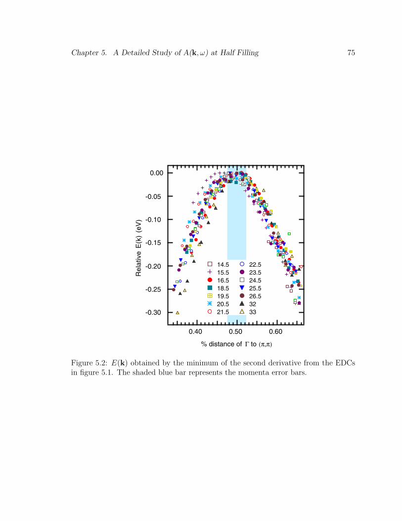
Chapter 5. A Detailed Study of A(k, ω) at Half Filling 75
-0.30
-0.25
-0.20
-0.15
-0.10
-0.05
0.00
0.600.500.40
14.5 22.5 15.5 23.516.5 24.5 18.5 25.519.5 26.5 20.5 3221.5 33
Rel
ativ
e E
(k)
(eV
)
% distance of Γ to (π,π)
Figure 5.2: E(k) obtained by the minimum of the second derivative from the EDCsin figure 5.1. The shaded blue bar represents the momenta error bars.

Chapter 5. A Detailed Study of A(k, ω) at Half Filling 76
12.011.010.0 12.011.0 12.011.0 12.011.0 12.011.0 13.012.011.0
Kinetic Energy (eV)
Inte
nsity
(A
rb. U
nits
)
16.5eV 16.7eV 16.9eV 17.1eV 17.3eV 17.5eV
Figure 5.3: EDCs from a single cleave of CCOC along the nodal direction forEγ=16.5eV to Eγ=17.5eV as indicated in each panel. The bold spectra indicates(π/2, π/2). The angular separation between the top and bottom spectra in eachpanel is 13◦ with an energy resolution, ∆E = 70meV. T=293K.
due to the energy cost associated with disrupting the antiferromagnetic order as
it hops away from its original location. The lowest energy state for the hole in
this potential corresponds to the Zhang-Rice singlet, while the first excited state is
predicted to lie roughly 1.8(J/t)2/3 ≈ 0.5eV higher in energy.[124] Although we are
not certain of the origin of the higher energy feature, the string resonance concept
provides an intriguing possibility for further study.
Having examined the dispersion, we now look at the more difficult problem of
extracting the underlying n(k) structure. It is of particular interest to determine

Chapter 5. A Detailed Study of A(k, ω) at Half Filling 77
-1.5 -1.0 -0.5 0.0-1.5 -1.0 -0.5 0.0
% d
ista
nce
from
Γ
to (
π,π)
Inte
nsity
(A
rb. u
nits
)
Binding Energy (eV)
36%
71%
Min Max
(π/2,π/2)
(a)
(b)
Figure 5.4: a) EDCs and b) corresponding image plot of CCOC taken along the nodaldirection with 23.5eV photons from figure 5.1. The bold spectra indicates (π/2, π/2).T=200K.
whether or not the underlying intensity profile of A(k, ω) has an asymmetry with
respect to the antiferromagnetic zone boundary as this would put constraints on
the valid coupling regime for different models. In figure 5.1 we noticed that for the
majority of photon energies the intensity of the lowest energy excitation begins to
lose weight before (π/2, π/2). This can be seen even more clearly in an image plot
for a characteristic set of data in figure 5.4. This has also been observed previously
by several authors with isolated photon energies.[25, 55, 54, 26, 120] In figure 5.5 the
n(k) curves obtained by integrating the EDCs in figure 5.1 from -0.5 to 0.3eV relative
to the valence band maximum for each photon energy are shown.1 Clearly, with the
1the energy integration window was chosen so as to minimize the contribution from the secondcomponent seen at higher binding energy, but we note that the results are independent of the specificenergy window chosen

Chapter 5. A Detailed Study of A(k, ω) at Half Filling 78
0.600.500.40
14.5 22.515.5 23.516.5 24.518.5 25.519.5 26.520.5 3221.5 33
% distance of Γ to (π,π)
Rel
ativ
e n(
k)
Figure 5.5: n(k) obtained by integrating the EDCs in figure 5.1 from -800meV to EF .The maxima of each curve were normalized to each other for display. The blue barrepresents the momenta error bars.
exception of 16.5, 32, and 33eV the intensity profile peaks well before (π/2, π/2),
which can also be seen from the EDCs themselves. This is evidence that a true
asymmetry exists in the data. This differs from the conclusions of a similar study
on SCOC, which used five photon energies from 20 to 24eV.[121] They observe the
intensity profile to be more heavily weighted towards (0,0) at Eγ=24eV which then
gradually shifts until at Eγ=20eV the profile is more heavily weighted towards (π, π).
From this one would conclude that the matrix elements are strong enough that the
true underlying n(k) can not be determined. However, the data from Figure 5.5 and
the majority of single photon energy studies on SCOC[25, 55, 54, 26, 120] suggests
otherwise.
As all of the above studies were only from a single cut through the Brillouin zone
we now examine a more global perspective of the intensity profile. Figure 5.6b)-f),

Chapter 5. A Detailed Study of A(k, ω) at Half Filling 79
presents relative n(k) patterns of CCOC over a Brillouin zone quadrant for five differ-
ent photon energies while panel a) is of an optimally doped Bi2212 sample. Spectra
are taken at the crosses and except for panel (c), the data has been symmeterized
about kx=ky and the geometry of the experimental setup was identical. The first two
panels reproduce the original comparison of metallic Bi2212 and insulating CCOC
from which the initial identification of a “remnant Fermi surface” was made.[53] For
a state with dx2−y2 orbital symmetry the suppression of weight as one approaches the
line kx=0 is expected. In Bi2212 the only drop in intensity which is not naturally
explained by matrix elements is where a Fermi surface crossing has occurred. As
seen in the figure the intensity drop matches the traditional method for determining
a Fermi surface crossing by following the dispersion by eye and is indicated by the
dots. A similar drop in intensity is observed in the insulator. Although the feature
is less well defined here, the striking resemblance it bears to the metal suggests that
the origin is similar, and hence it was qualitatively described as a remnant Fermi
surface.[53] [Note that the remnant Fermi surface is fully gapped by the large Mott
gap.]
Here we examine the effect of changing the photon energy. From panels (b)
through (f) one immediately notices that the intensity pattern varies tremendously
for the five photon energies: 25.2, 16.5, 29, 32.3, and 41eV. However, the variations
appear predominantly parallel to the (π, 0) to (0, π) direction, while perpendicular to
this there exists relatively little variation as we noted above in figure 5.2. The exact
shape of the remnant Fermi surface may change, but at all photon energies used there
is a loss of spectral weight as one crosses the approximate antiferromagnetic zone
boundary from (0, π) to (π, 0). It may appear that the remnant Fermi surface is more
hole-like or electron-like depending on the photon energy chosen, but the broadness
and the variability due to matrix elements prevent one from clearly identifying the
intensity profile as either case. However, the point which is clear from the data is
that globally, there is always an asymmetry in intensity stronger towards (0,0) than
towards (π, π) as one crosses the region spanned by the black lines in the Brillouin
zone which is also coincident with the antiferromagnetic zone boundary.

Chapter 5. A Detailed Study of A(k, ω) at Half Filling 80
c) 16.5eV d) 29eV
e) 32.3eV f) 41eV
a) Bi2212 b) 25.2eV
Γ (π,0)
(π,π)
Min.
Max.
Figure 5.6: (color) Integrated spectral weight. The crosses indicate where spectrawere taken. Except for (C) the data is symmetrized about the kx=ky line. Red ismaximum. (A) optimally doped Bi2212 at Eγ=22.4eV. The white hashed region indi-cates the approximate location of the Fermi surface determined from n(k). The dotsillustrate the position of the Fermi surface as determined by the traditional methodfor analyzing ARPES data. (B) CCOC shows a striking similarity of the insulator tothe metal allowing the identification of the white hashed region as a remnant Fermisurface. Comparison of (B) through (F) show CCOC taken at photon energies of25.2, 16.5, 29, 32.3, and 41eV. The intensity maxima varies between different pan-els, but the loss of intensity as one approximately crosses the antiferromagnetic zoneboundary is a consistent feature. The cumulative boundary of the remnant Fermisurface is drawn with black lines on panels (B) through (F). ∆E ≤ 70meV.

Chapter 5. A Detailed Study of A(k, ω) at Half Filling 81
Although the n(k) image plots can provide a wealth of information and are ex-
tremely good for summarizing data, it is important to look at the raw data to fully
appreciate the information being given by the image plots. This is done in Figure 5.7.
Panels (a) and (b) plot respectively, the EDCs from (0,0) to (π, π) and (π/2, π/2)
to (π, 0), from the data sets used to create the intensity maps in figure 5.6b)-f). We
find the spectra are qualitatively similar. This is true even at 41eV where the peak is
poorly defined throughout the zone. To examine them more closely, Figure 5.8 plots
both the dispersion of the peak position and n(k) together for all the cuts shown in
figure 5.7. As we saw before only slight differences exist in E(k) and n(k) among the
five different photon energies along (0,0) to (π, π). This however, contrasts sharply
with the (π, 0) to (0, π) cut. While the dispersion is again identical, the intensity
varies seemingly randomly. In the extreme case between 25.2eV and 29eV the inten-
sity is increasing as one approaches (π/2, π/2) for the former, and decreasing for the
latter.
Even for the case of a single two dimensional plane, the wavefunctions will have
some finite extent in the z-direction. Thus, the outgoing photoelectrons resulting
from photons with different wavelengths will necessarily have a different overlap, and
hence different cross-section, with the initial wavefunctions of the system. This is
impossible to avoid unless the initial wavefunctions z dependence were unrealistically
proportional to δ(z). The ideal way to eliminate such matrix element effects is to
average over all possible photon energies, and experimental geometries. Here we have
observed large variations along the antiferromagnetic zone boundary that are mani-
festations of the matrix element, while the asymmetric shift of weight towards (0,0)
with respect to the (π, 0) to (0, π) line is found to be a robust feature of the under-
lying spectral function. Our initial report implied that the underlying n(k) structure
matched that of the LDA Fermi surface at half filling without correlations.[53] It is
now clear, that the matrix elements are strong enough to make such a precise identi-
fication nearly impossible. However, we still conclude that an underlying asymmetry
exists in the spectral function about the antiferromagnetic zone boundary which is
robust despite variations with photon energy. Whether it truly lies along the LDA
Fermi surface, the antiferromagnetic zone boundary, or some other contour is an open

Chapter 5. A Detailed Study of A(k, ω) at Half Filling 82
-1 0
-1 0
-1 0-1 0-1 0-1 0
-1 0-1 0-1 0-1 0
Eγ = 16.5eV Eγ = 25.2eV Eγ = 29eV Eγ = 32.3eV Eγ = 41eV
Eγ = 16.5eV Eγ = 25.2eV Eγ = 29eV Eγ = 32.3eV Eγ = 41eV
Inte
nsity
(A
rb. u
nits
)
Binding Energy Relative to Valence Band Maximum (eV)
Binding Energy Relative to Valence Band Maximum (eV)
Inte
nsity
(A
rb. u
nits
)
a)
b)
0%
19
29
39
44
49
59
83
93
103
0%
11
32
43
53
64
75
86
96
107
21
0%
11
34
46
51
57
69
80
91
103
23
0%
13
39
53
66
79
92
105
26
98
10
39
0%
20
78
107
43
0%
21
86
64
0% 0%
0%
5%
11
34
57
80
103
26
53
79
105
17
28
39
50
61
71
82
93
43
88
65
22
Figure 5.7: (color) ARPES spectra along 2 cuts, (0,0) to (π, π) and (π/2, π/2) to(π, 0), and 5 different photon energies (16.5, 25.2, 29, 32.3, and 41eV). The intensitiesof the features vary, but the dispersion remains the same.

Chapter 5. A Detailed Study of A(k, ω) at Half Filling 83
-0.8
-0.6
-0.4
-0.2
0.0
-0.6
-0.4
-0.2
0.016.5eV25.2eV29eV32.3eV41eV
Rel
ativ
e E
(k)
(eV
)
Relative n(k) (A
rb. units)
Rel
ativ
e E
(k)
(eV
)
Relative n(k) (A
rb. units)
a) b)
(0,0) (π,π) (π,0) (0,π)(π/2,π/2) (π/2,π/2)
Figure 5.8: (color) Plots the peak position and n(k) from the spectra in figure 5.7.For both cuts the dispersion is independent of photon energy. The data along (π, 0)to (0, π) has been symmetrized. Along (0,0) to (π, π) the intensity has minor shifts,but is overall consistent indicating robustness of the remnant Fermi surface. For(π/2, π/2) to (π, 0) the intensity varies randomly indicating that this modulation in
intensity is due to matrix elements. Filled symbols indicate E( k) while open symbolsare for n(k).
question.
5.2.1 Eγ Discussion
What is the significance of this underlying intensity modulation? The question of
how a metal evolves into an insulator is one of the most fundamental in solid state
physics, and information on the evolution of n(k) would certainly provide insight
on this issue. For the case of non-interacting electrons, the Fermi surface shrinks
and eventually disappears as a band is filled. When electron-electron interactions
dominate, the situation is less clear. By considering the strong Coulomb interaction,

Chapter 5. A Detailed Study of A(k, ω) at Half Filling 84
Mott qualitatively described how a material predicted by band theory to be a metal
would in fact be an insulator.[16] However, it remains unclear as to how the details
of the electronic structure evolve from a half-filled metal to a Mott insulator. As the
Fermi surface which can be defined by the surface of steepest descent in the electron
momentum distribution function, n(k), is a characteristic features of any metal, an
equivalent question to the one above is how does the Fermi surface of a metal vanish
as strong electron correlations drive the system into an insulator?
In the context of specific many-body models such as the Hubbard model, it has
been shown that a structure in n(k) survives even when the on site Coulomb U drives
the system insulating, albeit the discontinuity in n(k) which existed in the metal has
been washed out.[38, 37, 39] This effect is linked to the fact that n(k) reflects the
underlying Fermi statistics of the electronic system. For the specific case of a two
dimensional square lattice that resembles the CuO2 planes of the cuprates, there is a
drop in n(k) across a line that is close to the antiferromagnetic zone boundary.[38, 37]
This is contrary to generalized t-J models where the structure in n(k) is washed
out.[37, 34]
By presenting n(k) we have implicitly used the sudden approximation to extract
the momentum distribution function, n(k), from ARPES data via the relation n(k)
=∫
A( k, ω)f(ω)dω where f(ω) is the Fermi function.[67] In the metallic state of opti-
mally doped Bi2212 the steepest descent of n(k) gives a Fermi surface consistent with
traditional ARPES analysis methods, despite the complication of matrix elements as
shown in figure 5.6. The intriguing result is that the n(k) pattern of the insulator,
CCOC, is strikingly similar to the n(k) pattern seen in Bi2212.[53] This realization,
coupled with many-body theoretical calculations on various forms of the Hubbard
model[38, 37], suggests that the insulator pattern contains information that is related
to a Fermi surface which has been destroyed by strong electron-electron interactions
thus giving a qualitative concept of a remnant Fermi surface as the surface of steepest
descent in n(k). In this chapter we have found that the remnant Fermi surface acts
to emphasize a robust feature which we observe in the insulator, although its precise
shape is uncertain. While this may not be a rigorous definition, as the Fermi surface
is only defined for a metal, this idea allows a practical connection from the pseudogap

Chapter 5. A Detailed Study of A(k, ω) at Half Filling 85
seen in underdoped cuprates to the properties of the insulator.[44]
However, the fact that the antiferromagnetic Brillouin zone boundary is quite
similar to the underlying Fermi surface (See figure 5.9a) will mean that the true origin
of this asymmetry will be uncertain. Therefore we suggest here a few ideal tests for
the RFS. One idea is to find a system whose non-interacting Fermi surface is radically
different from the antiferromagnetic Brillouin zone. For a hypothetical example see
figure 5.9b. To find such a single band strongly correlated two-dimensional system
compatible with ARPES may be a dream, particularly when considering that the
magnetic properties are a result of the electronic structure, but should at least be
kept in mind. Perhaps a more realistic approach will be to find a system similar to
the cuprates, but where the antiferromagnetic correlations are much smaller, such
that, at the measured temperature effects due to antiferromagnetic correlations could
be ruled out. We leave this as a hope for the future.
Returning to the photon energy dependence of the cuprates, we know they are
generally believed to be two dimensional electronic systems. However, as mentioned
above, only in the artificial case where the wavefunctions of each plane are propor-
tional to δ(z) will the electronic states probed by ARPES be independent of photon
energy. In reality the wavefunctions have some finite z extent, and even if they are
highly localized will have some finite overlap with neighboring planes. In fact such a
coupling must be present to create the observed three dimensional long range magnetic
order seen at half filling. Thus there exist several reasons which could cause E(k) to
depend on photon energy. Certainly, if the wave function overlap were large enough
to create a small dispersion as a function of kz such an effect would be expected. Al-
ternatively, if the matrix element had a significant dependence in the binding energy
of the feature which varied with photon energy, a photon energy dependent dispersion
would also result. Along similar reasoning, if there are multiple excitation branches
there is no reason to expect that the matrix elements dependence on photon energy
would be the same for each branch. Most likely an observed variation with photon
energy would be caused by a combination of several of these factors. However, in
figures 5.2 and 5.8 we have shown that the dispersion of the insulator is indepen-
dent of photon energy to within our experimental uncertainty. Three dimensionality

Chapter 5. A Detailed Study of A(k, ω) at Half Filling 86
a) CuO2 plane
b) Ideal test system
Band Theory U=0
A true remnant Fermi surface
Magnetism
U = 0OR
U = 0OR
Figure 5.9: Cartoons to illustrate differing ideas of the remnant Fermi surface ascorrelations are turned on (U�=0). Shaded regions indicate larger occupancy. Exper-imentally it is difficult to distinguish in the CuO2 plane whether the Fermi surfacesimply becomes washed out or whether the asymmetric n(k) is solely due to theantiferromagnetism present in the system. b) is a hypothetical case which couldeasily distinguish between the two cases, although it is questionable whether such astructure could even produce an antiferromagnetic ground state.
may still play a role in causing a small shift in dispersion with photon energy, but
it is a safe assumption to treat the electronic structure of the half filled insulator as
essentially two dimensional.
Recently, the role of the matrix element effects is also under examination regarding
the Fermi surface of Bi2212.[125, 126, 127] Several groups have reported the existence
of an electron-like Fermi surface centered at (0,0).[125] These groups report a subtle
change of dispersion near the flat band region around (π, 0), causing a change in the

Chapter 5. A Detailed Study of A(k, ω) at Half Filling 87
shape of the Fermi surface. Largely due to the difficulty in understanding the effects
caused by photoelectron matrix elements, there is no consensus in attempting to re-
solve this issue.[126] However, it would be very surprising to find the matrix element
purely responsible for causing an apparent change of the Fermi surface from hole-like
to electron-like with varying photon energy. More likely explanations include: disper-
sion in kz, bi-layer splitting[128, 129, 130], and phase separation. With the exception
of Pb doped samples Bi2212 also has the additional complication of superstructure in
the Bi-O planes. In Bi2212, it would be surprising for the dispersion in kz to have a
large effect considering the two dimensional nature of the cuprates. In reality though,
it is likely that all of these effects play roles which result in a potentially very complex
picture.
Interestingly, models which have multiple component electronic structures where
the wavefunctions and dispersions differ could have a simple explanation for the ob-
served controversy.[128, 129, 130] In such a case, variations in the matrix element
could now lead to different interpretations of the observed ARPES spectra at differ-
ent photon energies. This is possible because there may now be a different matrix
element for each component, and each matrix element may vary differently with pho-
ton energy. Thus causing one component to be more dominant at one photon energy
while hidden at another. This would naturally lead to different interpretations as a
function of photon energy. Thus we see that matrix element effects are not unique
to the oxychlorides, and care must be taken to extract the underlying single particle
spectral function from the ARPES data.
We have shown that the loss in intensity as one crosses the antiferromagnetic
zone boundary is a robust feature of the insulator, Ca2CuO2Cl2, which can not be
explained solely by matrix element effects. However, the photon energy dependence
does underscore the qualitative rather than quantitative nature of the remnant Fermi
surface concept. We argue that much physics can be learned in spite of the effect
which matrix elements can have in ARPES, as long as care is taken to properly sort
out the intrinsic versus the extrinsic physics. In particular, the resulting connection
between the d-wave like dispersion and the pseudogap in the underdoped regime is
robust.

Chapter 5. A Detailed Study of A(k, ω) at Half Filling 88
5.3 Rounded Node
Indeed, the greatest significance of the remnant Fermi surface as it pertains to the
high temperature superconductors is that a d-wave-like dispersion was identified in
the insulator, which could thus provide a natural connection between antiferromag-
netism and d-wave superconductivity. However, the earlier study on CCOC left some
ambiguity as to the precise nature of the dispersion near the nodal line, kx=ky.[53] A
simple d-wave dispersion proportional to | cos kxa − cos kya| would produce a linear
dispersion with a discontinuous derivative perpendicular to the nodal direction at
kx=ky. This is most easily seen by the fact that along the antiferromagnetic zone
boundary the above function reduces to | sin(kxa−π/2)|. Such a non-analytic disper-
sion is non-trivial, and hence the presence or absence of such a dispersion is of great
significance to theories which attempt to unify the antiferromagnetic insulator with
the d-wave superconductor.
In figure 5.10 we present EDCs taken at 0.6◦ intervals along the antiferromagnetic
zone boundary and through (π/2, π/2). One observes a smooth round dispersion
through (π/2, π/2). This is even more evident in the image plot of the same data.
To compare with the d-wave functional form we must quantify the dispersion seen
in the raw spectra. From the data one can see that the low energy features seen in
the insulator are inherently very broad. The half width at half max at (π/2, π/2)
is 100meV, which is on the order of the total dispersion seen in this material. Due
to this and the fact that the higher energy spectral weight is also dispersive and of
unknown origin, the significance of any particular fit to the data is questionable. For
this reason we have chosen to quantify the dispersion using three methods: the peak
maximum, the location of maximum curvature, and the leading edge midpoint. We
compare these quantites against | cos kxa − cos kya| in figure 5.11. The straight line
represents the simple d-wave scenario. Near the node it is clear that the dispersion is
rounded in each case.
One plausible explanation for the flatness of the dispersion near (π/2, π/2) could
be the dirty d-wave scenario. Previous ARPES work on underdoped Bi2212 samples
also found a flattened dispersion near the node of the superconducting and normal
Chapter 5. A Detailed Study of A(k, ω) at Half Filling 89
-1.5 -1.0 -0.5 0.0 -1.5 -1.0 -0.5 0.0
Binding Energy (eV)
Inte
nsity
(A
rb. u
nits
)Min. Max.
(π/2,π/2)
(a)
(b)
Figure 5.10: EDCs and corresponding image plot of Ca2CuO2Cl2 data taken alongthe antiferromagnetic zone boundary at 0.6◦ intervals. (π/2, π/2) is indicated by thebold EDC and the dotted line in the image plot. Data was taken at T=200K, 25.5eVphotons, ∆E = 40meV, and 0.8◦ angular resolution
state low energy pseudo gap [70, 97, 131]. In the earlier works this was mentioned to be
consistent with dirty d-wave since a finite density of states with zero excitation energy
would result in a flattening of the node region. However, Mesot et al. argue that the
flattening due to impurities can be ruled out since the pair breaking due to impurities
would cause the overall magnitude of the gap to decrease, while they observe the
opposite.[131] In other words, as the node region becomes flatter the maximum gap
value increases. Furthermore, we note that ACOC is very stable and must be very

Chapter 5. A Detailed Study of A(k, ω) at Half Filling 90
-0.4
-0.3
-0.2
-0.1
0.0
Rel
ativ
e B
indi
ng E
nerg
y (e
V)
1.00.80.60.40.20.0
|coskxa - cosk ya|/2
2nd Derivative Peak Position Leading Edge Midpoint Ronning et al. Science '98
Figure 5.11: Three methods for characterizing the dispersion of the data in figure5.10 plotted with the original data from ref. [53]. A straight line corresponds to asimple d-wave dispersion. Each curve was offset to zero at the node. Note that thed-wave-like gap is in addition to the Mott gap which is not shown. The increasedscatter as one approaches (π, 0) is indicative of the increased difficulty in tracing thedispersion away from (π/2, π/2).
chemically pure as evidenced by many unsuccessful attempts by many institutions to
dope the oxychlorides under atmospheric conditions[56]. The broadness of the peaks
can not be used as evidence for impurities since the same feature seen to be almost
equally broad in Bi2212 samples contain nearly resolution limited quasiparticle peaks
in their spectra in the superconducting state.[132] So, although one can not rule out
the possibility that the observed dispersion is due to impurities we will suffice it to
say that it remains a possibility, and will now focus our attention for the remainder
of this chapter on the more interesting assumption, that the observed rounding is
intrinsic to the undoped insulator.
In an attempt to quantify the deviation from a simple d-wave picture we fit the
data to ∆|B cos(2φ)+(1−B) cos(6φ)| in figure 5.12, where φ is described in the figure.

Chapter 5. A Detailed Study of A(k, ω) at Half Filling 91
-0.4
-0.3
-0.2
-0.1
0.0
Rel
ativ
e B
indi
ng E
nerg
y (e
V)
6040200ϕ (degrees)
(π,π)
(π,0)(0,π)
(0,0)
ϕ
2nd Derivative Peak Position Leading Edge Midpoint B=0.81; ∆=390meV B=0.82; ∆=410meV B=0.81; ∆=330meV
Figure 5.12: Fits of the data in figure 5.11 to ∆|B cos(2φ) + (1 − B) cos(6φ)| whereφ is indicated in the figure. B characterizes the deviation from a simple d-wave.
cos(2φ) is approximately | cos kxa−cos kya| and cos(6φ) is the next allowable harmonic
for d-wave symmetry. An increase in the cos(6φ) term (smaller B) corresponds to a
flatter nodal region. We find B=0.81± 0.01. This is smaller than any underdoped
sample measured by Mesot et al., and thus is consistent with their interpretation that
the rounding is a result of increasing antiferromagnetic correlations.[131]
Finally we note that the above data was taken at Eγ=25.5eV. Identical results
were obtained at Eγ=29eV, on a second cleave of CCOC at Eγ=25.5eV, and on SCOC
using 22.4eV photons. Improving the angular resolution by a factor of 4 by narrowing
the slits of our analyzer also had no effect.
5.3.1 Dispersion Discussion
We now address the significance of the rounded dispersion at (π/2, π/2). On simple
grounds, a sharp feature in k-space implies long range interactions in real space.
Considering that we are dealing with an antiferromagnet below the Neel temperature,

Chapter 5. A Detailed Study of A(k, ω) at Half Filling 92
this is what one might expect. However, we have found this not to be the case for
the dispersion in the nodal region. As a result, the photoemission spectrum, which
measures an excited state property, seems more to resemble a spin liquid state, where
the short range antiferromagnetic interactions are extremely important.
Numerical calculations show that the t-J model describes the dispersion from
(0,0) to (π, π) well, but incorrectly predicts the energy at (π/2, π/2) and (π, 0) to
be equal [38]. The addition of t′ and t′′ corrects this problem, and furthermore, for
realistic values of these parameters, shows that the dispersion is isotropic and scaled
by a single parameter, J .[105] The effect of adding t′ and t′′ to calculations is to
destabilize the single hole Neel state about (π, 0). The resulting state appears to be
a spin liquid state which may display spin charge separation, but this only occurs
about (π, 0).[105, 106] Perhaps this explains why RVB theories, which assume spin
charge separation throughout the entire zone, incorrectly predict a cusp at (π/2, π/2)
in the spinon dispersion while still correctly describing the overall dispersion on a
qualitative level.[44, 122]
The mean field treatment in a simple SDW applied to the Hubbard model which
includes up to third nearest neighbor hopping, fails.[105] The dispersion along (π, 0)
to (0, π) is much too great for realistic values. However, the dispersion does contain a
rounded node region. If one can argue why one should renormalize these parameters
as done by Nunez-Regueiro then it is possible to obtain a very good fit to the experi-
mental data.[133] Furthermore, they show that the magnitude of the overall dispersion
decreases with doping as has been seen in the high energy pseudogap. Alternatively
a diagramatic expansion of the Hubbard model containing t′ and t′′ also reproduces
the observed dispersion.[134] Finally, the SO(5) theory predicts a | cos kxa − cos kya|dispersion for the insulator when the superconductor has simple d-wave pairing.[123]
However, in the projected SO(5) the observed flattening of the node in the insulator is
consistent with a flattened dispersion observed near the node of the superconducting
gap as well.[99]

Chapter 5. A Detailed Study of A(k, ω) at Half Filling 93
5.4 Conclusions
In conclusion, our photon energy dependent study to extract the intrinsic spectral
function shows that the dispersion is indeed independent of photon energy, and that
despite a few exceptions an asymmetry exists in the n(k) about the line from (π, 0)
to (0, π). We also find that the dispersion along this contour does not fit a simple
d-wave dispersion, but is flattened near (π/2, π/2) consistent with similar rounding
observed in underdoped Bi2212 samples.[70, 97, 131] Numerical calculations on the t-
t′-t′′-J model which match all aspects of the insulator dispersion including the rounded
nodal region, show that the antiferromagnetic correlations are destroyed near (π, 0),
indicating that a spin liquid picture may be more appropriate for interpreting the
ARPES data.[105, 106] However, generalized t-J models fail to reproduce the observed
asymmetric intensity profile which is produced in the Hubbard model.[37, 38] Possibly
the Hubbard model including next nearest neighbor hopping terms [134] will be able
to capture all the physics of a single hole in the half-filled CuO2 plane.

Chapter 6
Na-doped Ca2CuO2Cl2
This chapter presents Angle Resolved Photoemission (ARPES) results on the doped
oxy-halide system, Ca2−xNaxCuO2Cl2. This is an ideal system to study the evolution
of the electronic structure across the metal to insulator transition, which may be the
key to unlocking the mystery of why the high temperature superconductors originate
as antiferromagnetic insulators. Due to material limitations La2−xSrxCuO4(LSCO) is
the only system to have been studied across the metal to insulator transition to date.
In this case, a two component electronic structure is observed, which is attributed
to microscopic phase separation.[42] It is currently still controversial whether the
behavior seen in LSCO is general to all the cuprates. Due to its superior surface
quality, the doped oxy-halides are a more natural choice to investigate these issues.
From ARPES we have found that Na-doped Ca2CuO2Cl2 contains fingerprints of
the parent insulator. This manifests itself in the form of “shadow bands”, a chemical
potential shift to the top of the valence band, and an extremely large pseudogap. In
addition, the low energy excitations (ie the Fermi surface) are best characterized as
a Fermi arc about (π/2, π/2). We also find evidence for an additional energy scale of
roughly 50meV in the hole-doped oxychloride.
94

Chapter 6. Na-doped Ca2CuO2Cl2 95
6.1 Experimental
Na-doped CCOC single crystals were grown by a flux method under high pressure, by
using a cubic anvil type pressure apparatus.[56] A powder mixture of Ca2CuO2Cl2,
NaCl, NaClO4, and CuO (1:0.2:0.2:0.1 molar ratio), sealed in a gold tube, was heated
up to 1250◦C and then slowly cooled down to 1050◦C under a high pressure (on the
order of 4 GPa). Uniform samples of varying Na concentration were achieved by using
different pressures during the synthesis. Crystals with a maximum dimension of 1.5
· 1.5 · 0.1 mm3 were obtained and cleaved easily in situ. The Na content, x, was esti-
mated by comparing the c-axis lattice constant with powdered ceramic samples.[89]
Magnetization measurements of Tc gave results consistent with the assigned doping
concentration. The Na concentrations used in this study were x=0.10(Tc=13) and
x=0.12(Tc=22K), which lie in the underdoped regime. As a reference, optimal Tc in
powder samples has been found to be 28K.[89] ARPES measurements were performed
solely on beamline 5-4 of SSRL. The measurement conditions are indicated in the first
caption of each new cleave which is presented.
6.2 Valence Band Comparison
Our investigation on Na-doped Ca2CuO2Cl2 begins with a comparison of the valence
band of the half-filled insulator and the metallic sample. In figure 6.1 valence band
spectra along the nodal direction are compared for x=0 and x=0.1. The data on
the insulator is consistent with previous reports,[114, 55] while the data for the Na-
doped Ca2CuO2Cl2 was reproduced on multiple cleaves. The low energy excitations
within 1eV of the chemical potential which the bulk of this chapter will focus on are
barely visible in this expanded scale. Generally, the two data sets are quite similar,
although differing relative intensities for a few of the bands about (0,0) can be seen.
The other difference is that the insulator is sharper than the metal, particularly near
(π, π). Perhaps this is an indication that the surface of Na-doped Ca2CuO2Cl2 is
not as well ordered as the pure sample grown under atmospheric conditions. Panel
6.1c plots the second derivative of the above spectra, which can be used to identify

Chapter 6. Na-doped Ca2CuO2Cl2 96
the dispersion of various features in the data. This method agrees with the visually
determined dispersion of the various bands in the insulator and the metal as shown
in panel 6.1d. With one minor exception, the resolved bands appear to have shifted
to lower binding energy with doping, as would be expected if this were a simple band
material. The discrepancy is from the metallic band at 5.5eV binding energy near
(0,0). However, due to the broadness of the metallic features, it is likely that this
band is a superposition of several peaks, and can not be rigorously compared to the
insulator. Note that several insulating bands are resolved in this same region. Thus,
the overall picture from the valence band data is suggestive of a chemical potential
shift with doping. The most convincing demonstration for this is at (π, π) where the
peaks for both hole concentrations are most clearly resolved. Here, the peak positions
indicate that the insulator is shifted to higher energy by roughly 300meV relative to
the metal. The naive expectation based on band structure calculations, which are
shown in figure 1.5, is a shift of roughly 100meV for an increased hole concentration
of 10%.[13, 95] The specific value of 300meV depends on which insulating data set is
used, since the chemical potential in the insulator can vary as much as the magnitude
of the Mott gap due to different pinning sites which exist for the different cleaved
surfaces. One could imagine that if the chemical potential of the insulator were pinned
at the peak position of the Zhang-Rice singlet at (π/2, π/2) then there would be no
shift of the chemical potential upon doping. However, this scenario is unphysical, as
the broad lineshapes of the insulator would then extend above the chemical potential,
which would imply that the system is metallic. This is clearly not the case. Thus,
a shift of 300meV is actually the minimum value one could get by comparing an
insulating data set to the data of the doped metallic sample presented in figure 6.1.
The valence band of our Na-doped CCOC crystals has a final peculiarity not
illustrated in the spectra discussed thus far. Namely, from 8 to 13eV binding energy
there exists several pronounced features which vanish extremely quickly with time.
This is shown in figure 6.2. The spectra from the cleave where these features were most
prominent is shown in the top panel. Features at 9, 10, and 12eV are visible which
we have never observed in the parent compound, CCOC. These features, however, do
not survive very long. 6.2b reveals that within 90 minutes following the initial cleave,
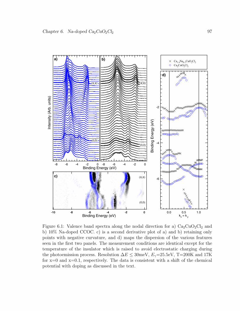
Chapter 6. Na-doped Ca2CuO2Cl2 97
-8 -6 -4 -2 0
-6
-4
-2
1.00.50.0
Ca1.9Na0.1CuO2Cl2 Ca2CuO2Cl2
-8 -6 -4 -2 0
kx = k y
(0,0) (0,0)
(π,π) (π,π)
-10 -8 -6 -4 -2 0-10 -8 -6 -4 -2 0
(0,0)
(π,π)
Inte
nsity
(A
rb. u
nits
)
Bin
ding
Ene
rgy
(eV
)
Binding Energy (eV)
Binding Energy (eV)
a) b)
c)
d)
Figure 6.1: Valence band spectra along the nodal direction for a) Ca2CuO2Cl2 andb) 10% Na-doped CCOC. c) is a second derivative plot of a) and b) retaining onlypoints with negative curvature, and d) maps the dispersion of the various featuresseen in the first two panels. The measurement conditions are identical except for thetemperature of the insulator which is raised to avoid electrostatic charging duringthe photoemission process. Resolution ∆E ≤ 30meV, Eγ=25.5eV, T=200K and 17Kfor x=0 and x=0.1, respectively. The data is consistent with a shift of the chemicalpotential with doping as discussed in the text.

Chapter 6. Na-doped Ca2CuO2Cl2 98
02 04 0
NaClO4
NaCl
a)
b)
c)
d)
Inte
nsity
(A
rb. u
nits
)
-16 -14 -12 -10 -8 -6 -4 -2 0
Binding Energy (eV)
(0,0)
(π/2,π/2) t = + 10 min t = + 90 min
t = + 20 min
Ca1.9 Na0.1 CuO2Cl2
Figure 6.2: a) reveals three features, at 9, 10, and 12eV, in Na-doped CCOC notpresent in the pure sample. the time elapsed between the initial cleave and the timethe spectra were recorded is indicated in the figure. b) illustrates, with a differentcleave, how the features vanish within 90 minutes of the initial cleave. The photonenergy was 25.5eV and the temperature was 10K and 20K for panels (a) and (b)respectively. The Fermi cutoff on the low energy spectral weight is too small to bevisible in this expanded scale. For comparison XPS spectra of NaClO4 (c) and NaCl(d) are also shown (from ref [135]), which are used in excess in the sample growth.
these features have vanished. For binding energies less than 7eV no change in the
spectra was ever observed over these time scales where particularly close attention
was paid to the near EF features. The photon energy was adjusted to ensure the high
binding energy features were not excited by a contribution of second order light from
the monochromator. Comparing the spectra in panels a) and b) suggests a dispersive
nature of these features. However, it was also observed that these features shift to
lower binding energy as they age. We tentatively assign the origin of these features to
molecules, such as NaCl and NaClO4 which are used in excess during the synthesis.
These loosely bound molecules are subsequently photodesorbed following the cleave.
Despite the uncertain nature of these high energy features, the fact that the low
energy features of the spectra have no variation over the short time scale where the
high energy features vanish, gives us confidence in our results on the Na-doped CCOC
crystals which follow below.

Chapter 6. Na-doped Ca2CuO2Cl2 99
6.3 Shadow bands
We now focus on an examination of the raw low energy spectral weight of a repre-
sentative cleave, which contain the features common to all cleaves. In this case the
Na concentration, x, is 0.10, which results in a Tc of 13.5K (∆Tc = 3.5K). The spec-
tra taken along (0,0) to (π, π) with a photon energy of 25.5eV are plotted in figure
6.3a. One can observe a broad feature develop near (0,0) and disperse toward the
Fermi level with increasing k. The crystal momentum with maximal intensity at the
Fermi energy occurs at (0.43π, 0.43π) which naturally coincides with the observed
sharp Fermi cutoff in the EDC. This coupled with a loss of spectral weight at larger k
values is representative of a band crossing the Fermi energy. However, this is not the
end of the story. Instead, as indicated by the tick marks, a feature is observed which
disperses away from the Fermi level as it loses weight rapidly. This feature is identi-
fied as a shadow band as it resembles the half filled insulator in which a band folding
about (π/2, π/2) occurs due to the long range antiferromagnetic ordering which exists
at half filling. In the insulator the magnetic order doubles the size of the unit cell
which, in turn, reduces the Brillouin zone by a factor of two. In actuality, the term
shadow band originates from calculations which show a similar folding of a band as
expected for long range order in a model where only short range correlations were
included.[45] Previously, Aebi et al. reported evidence for shadow bands in under-
doped Bi2212.[136] However, one is unable to distinguish whether or not the features
they observe result from a structural distortion or from underlying antiferromagnetic
fluctuations.[137] By contrast, to our knowledge, no structural distortion has ever
been reported on any of the doped or undoped oxy-halides.
Further examining the features about (π/2, π/2), figure 6.3b presents an image
plot of the data shown in figure 6.3a. One will notice, as seen in the EDCs, that there
is substantial weight after the Fermi crossing. Figure 6.3d shows MDCs at 300 and
600meV binding energy taken from the image plot in figure 6.3b. From this it is clear
that a single lorentzian will not suffice to properly fit the data. A second lorentzian is
necessary, indicating that the band disperses back as the separation between the two
lorentzians grows with increasing binding energy. Finally, the shadow band will also

Chapter 6. Na-doped Ca2CuO2Cl2 100
-1.2 -0.8 -0.4 0.0-0.6 0.0-1.2 -0.8 -0.4 0.0
-0.6 eV
-0.3 eV
E-EF (eV) E-EF (eV)E-EF (eV)
Inte
nsity
(A
rb. u
nits
)
Inte
nsity
(A
rb. u
nits
)
(0,0) (π,0)
(π,π)(0,π)
(0,0) (π,π)
(0,0)
(π,π)(π,π)
(0,0)
(π,0)
(a) (b) (c)
(d)
Figure 6.3: a) and c) EDCs of Na-doped CCOC along high symmetry directions asshown in the cartoon. b) An intensity plot from the spectra shown in a). d) MDCsalong (0,0) to (π, π) revealing a band dispersing back. Resolution ∆E ≤ 23meV,x=0.10, T=10K, and Eγ=25.5eV

Chapter 6. Na-doped Ca2CuO2Cl2 101
Inte
nsity
(A
rb. u
nits
)
-0.8 -0.6 -0.4 -0.2 0
Binding Energy (eV)
(0.4π,0.4π)
(π,0)
(π,0.3π)
10% Na doped CCOC10% Dy doped Bi2212
Figure 6.4: Comparison of EDCs at selected k points of 10% Dy-doped Bi2212 (takenfrom ref [71] and 10% Na-doped CCOC (from figure 6.3). The Na-doped CCOCsystem suggests a much larger pseudogap than in Bi2212, both for the low energypseudogap (thick bars) and the high energy pseudogap (triangles).
be apparent in the second derivative plot shown in figure 6.5. This demonstrates that
a broad feature in Na-doped CCOC pulls back and loses weight rapidly after reaching
a maximum near (π/2, π/2), which we identify as evidence for a shadow band.
Along with the unusual features from (0,0) to (π, π) we also find some surprises in
the data from (0,0) to (π, 0) to (π, π) which are displayed in figure 6.3c. Although a
broad feature is apparent, it never seems to reach the Fermi energy. Instead it simply
appears to lose weight as it reaches (π, 0) and vanishes completely on its approach to
(π, π). This is in sharp contrast to the data along the nodal direction where a clear
Fermi cutoff indicating a Fermi level crossing is observed. In comparison with other

Chapter 6. Na-doped Ca2CuO2Cl2 102
cuprates, the lack of a Fermi cutoff would normally be identified as an extremely large
pseudogap, the origin of which, remains as a longstanding question. In an attempt
to quantify this suppression of weight, we compare 10% Na-doped CCOC to 10% Dy
doped Bi2212[71] in figure 6.4. One clearly observes the loss of spectral weight at the
Fermi energy for the Fermi momentum of (π, 0.3π) when compared to the respective
Fermi crossings along the nodal direction near (0.4π, 0.4π). There are two common
methods for characterizing the pseudogap with ARPES. The first, is by the shift of the
leading edge midpoint of a spectra to higher binding energy relative to the chemical
potential as indicated by the dashed lines. This is typically referred to as the low
energy pseudogap. For Dy-doped Bi2212 this is reasonably well defined, and gives
a value of 30 meV. For the Na-doped CCOC sample, we find a value of 65 meV at
(π, 0.3π) and 130 meV at (π, 0). However, this result is a bit tenuous, as the Na-doped
CCOC spectra in figure 6.4 do not provide us with a clear leading edge. In this case
we are more inclined to characterize the pseudogap by the high energy pseudogap
which is the identification a larger energy scale in the spectra about (π, 0), and is
sometimes referred to as a “hump”.[74] Here, we find a high energy pseudogap of
roughly 300meV for Na-doped CCOC, compared with 120meV for Dy doped Bi2212
as indicated by the triangles in figure 6.4. Independent of the method chosen, the
pseudogap for Na-doped CCOC appears significantly larger than that of Bi2212 at
a comparable doping level. Notice though, that the pseudogap of 300meV at (π, 0)
in Na-doped CCOC is comparable to the d-wave gap modulation seen in the half-
filled insulator. Indeed, the overall features observed in Na-doped CCOC are quite
reminiscent of the features of the insulator.
A final characterization of the data, is that in the vicinity of (π/2, π/2), the spectra
indicate the presence of two components as noted by the tick marks. We will come
back to this point in the section on lineshapes.
6.4 Chemical potential shift
As the Na-doped CCOC data suggests a similarity to the half filled insulator we
now focus on a more detailed comparison of the doped and undoped oxy-chloride.

Chapter 6. Na-doped Ca2CuO2Cl2 103
-1.0
-0.5
0.0
-1.5
-1.0
Bin
ding
Ene
rgy
(eV
)
Γ (π,0)(π,π) Γ
Figure 6.5: Second derivative intensity plots of the x=0.10 data shown in figure 6.3and of a half filled sample taken from ref [53]. The dispersion is nearly identical asidefrom the fact that the insulator lies roughly 700meV below the chemical potential.This suggests a shift of the chemical potential upon doping the antiferromagneticinsulator.
Figure 6.5 plots the second derivative in gray scale of the doped sample first shown
in figures 6.3a and 6.3c along side the second derivative of the undoped data in color
originally presented in ref [53]. Immediately one will notice that the dispersion is
nearly identical. Along (0,0) to (π, π) a band disperses towards the Fermi level, is
maximum near (π/2, π/2), and loses weight rapidly as it pulls back to higher binding
energy. Meanwhile, the minimum binding energy along (0,0) to (π, 0) to (π, π) lies
roughly 300meV below the minimum of the nodal direction. In fact, the only difference
between the insulator and the metal seems to be that the band in the metal intersects
the Fermi energy near (π/2, π/2) while the minimum binding energy of the insulator
at (π/2, π/2) lies 700meV below the chemical potential. It appears that the broad
features seen in the metal originate from the insulator.
To further support this idea figure 6.6 presents spectra along the entire (0,0) to
(π, 0) and (0,0) to (π, π) lines, with the chemical potential of the insulator shifted by
650meV. Along (0,0) to (π, 0) the spectra are remarkably similar. In many instances
fine details of the line shape match perfectly. For example, a second broad component
in the electronic structure can be observed at roughly 600meV higher binding energy

Chapter 6. Na-doped Ca2CuO2Cl2 104
from the first feature.1 This indicates that upon doping, the chemical potential
simply drops to the top of the valence band similar to the case of an ordinary band
material. This would naturally explain the large high energy pseudogap seen at (π, 0)
as a remnant property of the insulator as first suggested by Laughlin.[44, 53] The
apparent discrepancy between 650meV and 300-400meV obtained by the low energy
and valence band spectra, respectively, is due to different pinning sites for different
insulating data sets as discussed earlier.
Along (0,0) to (π, π) the situation is less clear. As the feature moves towards lower
binding energy a sharp Fermi cutoff appears in the metallic samples, as anticipated
by the large peak at the Fermi level from the energetically shifted spectra of the
insulating sample. However, the match between the spectra becomes increasingly
worse as (π/2, π/2) is approached. The weight at (π/2, π/2) is simply suppressed
relative to the insulator, perhaps simply indicating that a Fermi crossing has indeed
occurred before (π/2, π/2). The Na-doped CCOC sample was even rotated by 45
degrees for the (0,0) to (π, π) cut relative to the other three sets of data so as to
maximize the cross section along the nodal direction for an initial state with dx2−y2
symmetry. Perhaps this indicates that increased scattering which could effectively
smear out the k resolution, and thus have the greatest effect where the dispersion is the
steepest, is responsible for this suppression. However, this would require a nontrivial
scattering mechanism, which does not simply produce an angle averaged background.
Also, the cleavability of the Na-doped compounds is the same as the parent insulator,
and laser reflections from the sample indicate flat surfaces, which argue against angle
averaging as the cause for the observed suppression of weight. Typically, highly angle
dependent valence band spectra as shown in figure 6.1 are indicative of a good surface,
although the Na-doped valence band features are somewhat broader than in the case
of the insulator. In this regard, a broadened feature at (π/2, π/2) is not unexpected
considering the observation by Pothuizen et al. who noted that in SCOC the lineshape
of the 2eV binding energy peak at (π, π) is identical to the lineshape of the Zhang-Rice
singlet at (π/2, π/2).[55] This suggests that the small differences between the doped
system and the half filled insulator may indeed result from a difference in sample
1A brief discussion on this high energy feature is in chapter 5

Chapter 6. Na-doped Ca2CuO2Cl2 105
-1.2 -0.8 -0.4 0.0-1.2 -0.8 -0.4 0.0
Ca2CuO2Cl2 Ca1.9Na0.1CuO2Cl2
Γ −> (π,0) Γ −> (π,π)
Binding Energy (eV)
Inte
nsity
(A
rb. u
nits
)
19%
38%
48%
57%
67%
76%
86%
95%
105%
19%
38%
48%
57%
29%
81%
90%
100%
0%
43%
Figure 6.6: EDCs of Ca2CuO2Cl2 (blue) taken from ref [53] are shifted by 650meV andare compared with EDCs of 10% Na-doped CCOC(black). The overlap is extremelygood with the exception of the features near (π/2, π/2). The data is normalized athigh binding energy for comparison. The slight rise in spectral weight above EF ob-served in some EDCs of CCOC is due to the presence of a core level excited by secondorder light. This is not present in the metallic sample where the second order lightcontribution is heavily suppressed by the use of a normal incidence monochromator asopposed to a grazing incidence monochromator for the insulating data. Eγ=25.5eV,T=100K and 10K for x=0 and x=0.1, respectively.

Chapter 6. Na-doped Ca2CuO2Cl2 106
quality.
6.4.1 Eγ dependence versus the Insulator
Considering that the features of hole doped CCOC track the dispersion of the fea-
tures in the half filled insulator, one might wonder exactly how similar the electronic
states are for the two doping levels. As previously discussed in this dissertation,
the spectral function of interest is modulated by a matrix element which under the
dipole approximation can be written as |〈Ψf |A · p|Ψi〉|2 where Ψi,f are the initial
and final state wavefunctions, and A · p is the perturbing Hamiltonian (See chapter
12.512.011.511.0 13.513.012.512.0 12.011.511.010.5 13.012.512.011.5
Ca1.9Na0.1CuO2Cl2 Ca2CuO2Cl2
Kinetic Energy (eV)
Inte
nsity
(A
rb. u
nits
)
16.5eV 17.5eV
Kinetic Energy (eV)
Inte
nsity
(A
rb. u
nits
)16.5eV 17.5eV
Γ
(π,π)
(0,π)
Figure 6.7: Photon energy dependence along the nodal direction forCa2−xNaxCuO2Cl2 for x=0.1 and x=0. For each doping, the same k range is shown,while the photon energy is indicated in each panel. T=10K and 293K for x=0.1 and0.0, respectively. Notice, that the modulation of intensity varies with photon energyin a similar fashion for both dopings.
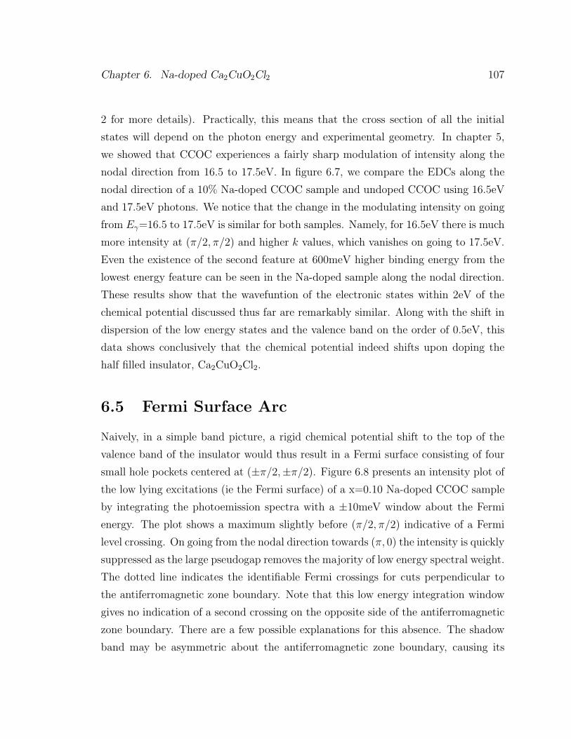
Chapter 6. Na-doped Ca2CuO2Cl2 107
2 for more details). Practically, this means that the cross section of all the initial
states will depend on the photon energy and experimental geometry. In chapter 5,
we showed that CCOC experiences a fairly sharp modulation of intensity along the
nodal direction from 16.5 to 17.5eV. In figure 6.7, we compare the EDCs along the
nodal direction of a 10% Na-doped CCOC sample and undoped CCOC using 16.5eV
and 17.5eV photons. We notice that the change in the modulating intensity on going
from Eγ=16.5 to 17.5eV is similar for both samples. Namely, for 16.5eV there is much
more intensity at (π/2, π/2) and higher k values, which vanishes on going to 17.5eV.
Even the existence of the second feature at 600meV higher binding energy from the
lowest energy feature can be seen in the Na-doped sample along the nodal direction.
These results show that the wavefuntion of the electronic states within 2eV of the
chemical potential discussed thus far are remarkably similar. Along with the shift in
dispersion of the low energy states and the valence band on the order of 0.5eV, this
data shows conclusively that the chemical potential indeed shifts upon doping the
half filled insulator, Ca2CuO2Cl2.
6.5 Fermi Surface Arc
Naively, in a simple band picture, a rigid chemical potential shift to the top of the
valence band of the insulator would thus result in a Fermi surface consisting of four
small hole pockets centered at (±π/2,±π/2). Figure 6.8 presents an intensity plot of
the low lying excitations (ie the Fermi surface) of a x=0.10 Na-doped CCOC sample
by integrating the photoemission spectra with a ±10meV window about the Fermi
energy. The plot shows a maximum slightly before (π/2, π/2) indicative of a Fermi
level crossing. On going from the nodal direction towards (π, 0) the intensity is quickly
suppressed as the large pseudogap removes the majority of low energy spectral weight.
The dotted line indicates the identifiable Fermi crossings for cuts perpendicular to
the antiferromagnetic zone boundary. Note that this low energy integration window
gives no indication of a second crossing on the opposite side of the antiferromagnetic
zone boundary. There are a few possible explanations for this absence. The shadow
band may be asymmetric about the antiferromagnetic zone boundary, causing its

Chapter 6. Na-doped Ca2CuO2Cl2 108
1.0
0.5
0.0
k y (
π/a)
1.00.50.0kx (π/a)
Γ (π,0)
(π,π)(0,π)
Figure 6.8: Intensity Plot of the low energy excitations. (red is maximum) The dottedline is a guide to the eye, indicating where a clear Fermi cutoff was identified. Theblack lines mark high symmetry directions through the Brillouin zone. Resolution∆E ≤ 14meV, x=0.10, T=22K, the integration window is ±10meV about the Fermienergy, and HeIα radiation (Eγ=21.2eV) was used as the photon source.
Fermi crossing to occur at the same momenta as the main band. Alternatively, the
coherence factors associated with the shadow band are possibly such that the second
crossing is indistinguishable from the background signal.[45] The latter scenario would
be surprising considering that the shadow band is clearly evident at higher binding
energies. This suggests that perhaps the shadow band and the low energy excitations
responsible for the image in Figure 6.8 result from two separate components of the
spectral function: a high energy one associated with the observed shadow band, and
a separate component responsible for the Fermi surface which is most well described

Chapter 6. Na-doped Ca2CuO2Cl2 109
as a Fermi Arc about (π/2, π/2). Below we will see more evidence for this picture.
6.6 Lineshapes and Dispersion
We begin an examination of the lineshapes with another look at the spectra near
(π/2, π/2). From the earlier cleave presented in figure 6.3 we alluded to the existence
of two components in the electronic structure near (π/2, π/2). Figure 6.9 presents
EDCs perpendicular to, and along the Fermi arc shown in figure 6.8. Now, in the
-0.4 -0.2 0.0-1.0 -0.8 -0.6 -0.4 -0.2 0
Γ (π,π)Γ (π,π)
(π,0)
Binding Energy (eV)
Inte
nsity
(A
rb. u
nits
)
Figure 6.9: EDCs perpendicular to and along the Fermi arc of figure 6.8, as indicatedby the cartoon above the respective stack of EDCs. Note that two components can beseen for the spectra in the vicinity of kF along the nodal direction. x=0.10, T=22K,and HeIα radiation (Eγ=21.2eV) was used as a photon source.

Chapter 6. Na-doped Ca2CuO2Cl2 110
vicinity of the Fermi crossing in the nodal direction, two components in the EDCs
are clearly observed. The higher energy feature loses weight rapidly as it pulls back
away from the Fermi surface in a fashion reminiscent to the insulating feature as
discussed earlier, while the sharper, lower energy feature appears to have a more
conventional behavior associated with a Fermi crossing. From (0,0) to (π, π) this
feature emerges from the higher energy feature on its approach towards (π/2, π/2),
sharpens, and then, crosses the Fermi level. The loss of the two component structure
as one approaches (π, 0) is again indicative of the observed large pseudogap, which
precludes the identification of any similar structure in the low energy excitations
near (π, 0). The reason for the difference in clarity of this structure between cleaves
is unknown, but may be due to a variation of inhomogeneities and experimental
conditions between different cleaves. Note, that the presence of the sharp low energy
feature is a tribute to the high quality of these samples.
An alternative method to study the electronic structure is through the use of
MDCs. In figure 6.10a we present MDCs along the nodal direction for the same data
presented in figure 6.9 as EDCs. The red curves show the quality of single lorentzian
fits to selected MDCs. Similar good agreement in other cuprates has been used as
justification for extracting self energies from the fit parameters, as discussed in chapter
2 [138, 139, 140]. In the following section we will perform a similar analysis, but here
they simply serve as a method for parameterizing the observed dispersion. Figures
6.10b and 6.10c plot the peak positions and widths as a function of the binding energy
of the corresponding MDCs. A change of slope in the dispersion of the peak positions
at 56meV is indicated by the arrow. This value is attained from the intersection of two
linear fits ranging from 0 to 30meV and 100 to 200meV. We shall refer to this feature
as a “kink”. A similar kink in other cuprate systems has received significant attention
in recent ARPES literature.[139, 140, 141, 142] Another change in slope at roughly
350meV is ignored as it is likely to be an artifact of matrix elements and contributions
from a broad band roughly 600meV higher in binding energy. Note, that the width
of the peak is roughly linear at very high energy, but there also appears to be a more
rapid change in width at approximately 80meV binding energy.
A peculiar feature of the MDCs in figure 6.10 is that the shadow band which we

Chapter 6. Na-doped Ca2CuO2Cl2 111
0.14
0.12
0.10
0.08
0.06
Hal
f-w
idth
(fr
actio
n of
Γ
−> (π
,π)
cut)
-0.5 -0.4 -0.3 -0.2 -0.1 0.0
Binding Energy (eV)
Inte
nsity
(A
rb. u
nits
)
0.60.50.40.3
distance from Γ −> (π,π)
0.460.440.420.400.38
Peak Position (% of Γ −> (π,π) cut)
-0.5
-0.4
-0.3
-0.2
-0.1
0.0
Bin
ding
Ene
rgy
(eV
)
EF
-0.5 eV
(a)(b)
(c)
Figure 6.10: a) Sample MDCs of the nodal direction data from figure 6.9. Singlelorentzian fits to selected MDCs are overlayed in red. Respectively, b) and c) givethe peak positions and widths (half width at half maximum) from the MDC analysis.The arrow in b) indicates the kink energy, as discussed in the text.

Chapter 6. Na-doped Ca2CuO2Cl2 112
had discussed before is not evident in this set of data. To understand this, one must
realize that the photon energy was different between the two cleaves shown in figure
6.3 and figure 6.9. This indicates that matrix elements are responsible for determining
the relative intensity between the main band and the shadow band. Thus, by varying
the photon energy we may hope to bring to light all the different excitations in the
system even if they are not all present at one single photon energy. In figure 6.11
EDCs of yet another cleave, this time a x=0.12 Na-doped CCOC sample, is presented
along the nodal direction for two different photon energies. At Eγ=16.5eV the peak-
dip-hump structure is clearly observed, while at Eγ=21.0eV the hump is suppressed
-0.3 -0.2 -0.1 0.0-0.3 -0.2 -0.1 0.0
Binding Energy (eV)
Eγ = 16.5 eV Eγ = 21 eV
Inte
sity
(A
rb. u
nits
)
30%
56%
32%
50%
Figure 6.11: EDCs from a x=0.12 sample along the nodal direction for two differentphoton energies. Note that the broad high energy hump is suppressed upon changingto the higher photon energy. The dashed lines mark the dip position in the Eγ=16.5eVdata, and are redrawn on the Eγ=21.0eV data. Resolution ∆E ≤ 15meV, and T=8K.Other than the photon energy and an adjustment of the outgoing electron angles inorder to measure the same k range, the measurement conditions are identical.

Chapter 6. Na-doped Ca2CuO2Cl2 113
to the extent that a dip is no longer observed at kF . Although we can not distinguish
whether the hump feature has been suppressed or the sharp peak has been enhanced,
it is clear that the ratio of the two peaks varies significantly with photon energy.
Next, let us examine the MDC analysis which further illustrates the differences
between the two photon energies. From the MDCs in figure 6.12 it is clear that two
lorentzians are necessary for a reasonable fit to the Eγ=16.5eV data, while a single
lorentzian is sufficient at Eγ=21.0eV. Again we see an instance where the shadow
band is present under one set of experimental conditions and not the other. What is
remarkable is that the shadow band in the Eγ=16.5eV data becomes weaker as one
approaches the Fermi energy, while the main band sharpens and is more well defined.
This is completely counterintuitive. One would expect that the coherence factors
0.50.40.30.20.50.40.30.2
distance of Γ −> (π,π)
Inte
sity
(A
rb. u
nits
)
Eγ = 16.5 eV Eγ = 21 eV
EF
-0.4eV-0.4eV
EF
Figure 6.12: Sample MDCs from the data in figure 6.11. Fitting curves are in color.Note that two lorentzians are necessary to fit the Eγ=16.5eV data, while a singlelorentzian is sufficient for the Eγ=21.0eV data.

Chapter 6. Na-doped Ca2CuO2Cl2 114
which regulate the intensity of the shadow band to become stronger, not weaker,
as the Fermi energy is approached. Thus, either the low and high energy parts of
the shadow bands have different origins, or their wave functions have significantly
different character which permits one to find a photon energy where the low energy
portion of the shadow band is suppressed relative to the high energy part. In the
latter case, one would expect that by searching hard enough one should be able to
find a situation where the converse is true, which to this point we have not. In any
event, this certainly is not a typical shadow band.
From the MDCs one can extract the dispersion of the various features by fitting the
peaks to one or more lorentzians. The peak positions from the fits to the data in figure
6.12 are shown in figure 6.13. If one could legitimately identify the peak positions
with a single dispersing band with a corresponding shadow, then the Eγ=16.5eV data
would be quite remarkable. It shows a kink in the main band near 50meV as observed
before, while the shadow band exhibits a much steeper dispersion, a Fermi crossing
which is not symmetric to the main band with respect to the antiferromagnetic zone
boundary, and a possible kink, which is very difficult to identify if it exists at all.
Meanwhile, the MDC data in figure 6.10 and the Eγ=21.0eV data in figure 6.12 lack
the second component expected for a band which is bending back. A second lorentzian
indicating the existence of a shadow band can not be ruled out, but the quality of
the single lorentzian fits implies that the matrix elements conspire such that it does
not give a significant contribution under these experimental conditions. Note that
when using polarized 21eV photons, the sharp feature which appears to cross the
Fermi energy is significantly enhanced relative to the hump like feature as seen by the
EDCs in figure 6.11. This fortuitous photon energy is thus the best opportunity for
an MDC analysis to examine the details of the dispersion of this seemingly isolated
band. In figure 6.13 the Eγ=21.0eV peak position data also show a rounded kink
at 50meV. This suggests that an energy scale of roughly 50meV indeed exists in Na-
doped CCOC as indicated earlier in figure 6.10. It is remarkable that despite the
tremendous variation in photon energy which calls into question the assignment of a
single feature in the MDC analysis, particularly at Eγ=16.5eV, the kink in the main
band lies at the same energy independent of the conditions.

Chapter 6. Na-doped Ca2CuO2Cl2 115
0.550.500.450.400.35-0.30
-0.25
-0.20
-0.15
-0.10
-0.05
0.00
0.440.420.400.38-0.30
-0.25
-0.20
-0.15
-0.10
-0.05
0.00
Eγ = 16.5 eV Eγ = 21 eVB
indi
ng E
nerg
y (e
V)
Bin
ding
Ene
rgy
(eV
)
distance of Γ −> (π,π) distance of Γ −> (π,π)
Figure 6.13: Peak positions of the lorentzian fits of the MDCs shown in figure 6.12for a x=0.12 sample. The blue lines are guides to the eye. Note the “kink” positionof roughly 50meV in the main band dispersion at both photon energies, while theshadow band has a significantly steeper dispersion. The dashed lines are the same asthose in figure 6.11 where they were marking the boundary of the dip location in theEγ=16.5eV data. Here they serve well to mark the approximate kink position of themain band.
The k dependence of the kink is not clear. It appears to be washed out as one
moves away from the nodal direction, but this may be a combination of two effects.
First, the dispersion flattens out at higher energy as one approaches the Van Hove
singularity, and second the high energy pseudogap removes spectral weight which
prevents a clear identification of the dispersion near EF . Samples where the high
energy pseudogap is not as imposing will be necessary to elucidate the k dependence
of the kink.

Chapter 6. Na-doped Ca2CuO2Cl2 116
6.6.1 Temperature dependence of the peak-dip-hump
The peak-dip-hump structure in Na-doped CCOC may remind one of the peak-dip-
hump structure first seen in Bi2212[143, 144], and now in YBCO[145] and Bi2223[146]
as well. The striking aspect of this feature in Bi2212, Bi2223, and YBCO is that the
peak appears to turn on at Tc. However, one should note that the peak-dip-hump
structure observed here is along the nodal direction, while in the others it is seen at
(π, 0). So one would like to know if the peak-dip-hump structure observed in Na-
doped CCOC is at all related with Tc. Figure 6.14 shows a temperature dependence
of EDCs along the nodal direction which display the peak-dip-hump structure at
10K. It is clear that this structure survives well past the transition temperature of
22K all the way to 75K, after which it becomes smeared out. The temperature was
then cycled back down to 10K to ensure that the broadening was not due to an aging
-0.3 -0.2 -0.1 0.0 -0.3 -0.2 -0.1 0.0 -0.3 -0.2 -0.1 0.0 -0.3 -0.2 -0.1 0.0 -0.3 -0.2 -0.1 0.0 -0.3 -0.2 -0.1 0.0
Binding Energy(eV)
Inte
nsity
(A
rb. u
nits
)
T=10K T=25K T=45K T=75K T=120K T=10K
Figure 6.14: Temperature dependence of EDCs along kx=ky taken with Eγ=16.5eV,and ∆E ≤ 15meV. The spectra were taken from left to right as a function of time.As Tc=22K for this x=0.12 Na-doped CCOC sample, we see that the two componentstructure observed here is not related to superconductivity.

Chapter 6. Na-doped Ca2CuO2Cl2 117
sample. Therefore the peak-dip-hump structure in the nodal direction of Na-doped
CCOC is certainly not a result of superconductivity. The MDC analysis of this data
is similar to the Eγ=16.5eV data shown in figures 6.12 and 6.13. The peak position
of the main band as a function of temperature is shown in figure 6.15, from which, it
can be seen that the kink is also unaffected through Tc.
k
-0.25
-0.20
-0.15
-0.10
-0.05
0.00
Bin
ding
Ene
rgy
(eV
)
T = 10 K T = 25 K T = 45 K T = 75 K T = 120 K T = 10 K
Figure 6.15: Peak positions of the main band in an MDC analysis of the data shownin figure 6.14. They have been offset in k for clarity, and the second band necessaryfor a reasonable fit to the data is not shown. The solid lines are guides to the eye,and the dashed lines give estimated limits for the energy of the “kink”, and the datawere taken from left to right as a function of time.
6.6.2 Self Energy, Σ
As the Eγ=21.0eV data suggests that only a single component has a significant contri-
bution to the observed spectra, it is tempting to assign the lorentzian fit parameters
to expressions containing the real and imaginary parts of the self energy, as discussed
in chapter 2. To do this one must first make an assumption on the form of the
bare dispersion, εk. Here, we let εk = vF · (k − kF ), and determine vF by setting
ReΣ(−0.2eV ) = ReΣ(EF ) = 0. The choice of -0.2eV is arbitrarily chosen so as to

Chapter 6. Na-doped Ca2CuO2Cl2 118
lie at a higher binding energy than the kink energy scale, but at energies less than
where the fits give a non-sensical dispersion. This choice is consistent with previous
studies [140, 142], where -0.2eV is chosen because at higher binding energy a single
lorentzian no longer produces a satisfactory fit. The quality of the single lorentzian
fits here up to 500meV is likely to be accidental, as a second high energy component
exists. The fact that we can not identify a clear point at which the MDC analysis
begins to fail brings into question the validity of this procedure as a whole. However,
we proceed on the assumption that setting ReΣ = 0 as done for Bi2212 and LSCO
is also reasonable for Na-doped CCOC. This gives vF = 4.93eV A, and the resulting
real and imaginary parts of the self energy are shown in figure 6.16.
From ReΣ we see the effect of the kink near 60meV, and the arbitrary nature of
setting ReΣ = 0 at -0.2eV. Note however, that setting ReΣ = 0 at any other value
would not affect the qualitative features observed here. Now, let us assume that we
can break up the self energy into three terms: electron-electron, electron-phonon and
impurity scattering. For the imaginary part of the self energy we can take the impurity
contribution to be a constant, and in a simple model the electron-phonon term will
also be a constant above the Debye frequency. Thus electron correlations are solely
responsible for the high energy part of ImΣ under these approximations. In figure
6.16 we fit the imaginary part of Σ from -0.2 to -0.3eV with both a quadratic term
and a linear term. The former being representative of a Fermi liquid scenario, while
the latter is expected for a marginal Fermi liquid. Aside from the constant impurity
term determined by ImΣ(EF ), the residual contribution, given by the dotted lines,
is presumably purely an electron-phonon scattering term. Interestingly, the point
of steepest descent of the electron-phonon contribution, independent of using the
quadratic or linear fit, is roughly 50meV, which is equal to the kink energy which
we identified earlier. The near linear scattering rate seen here in ImΣ up to high
energies is reminiscent of marginal Fermi liquid behavior.[147] However, if a pure
marginal Fermi liquid picture were responsible for the observed behavior of the self
energy then a sharp kink can not exist as there is no additional energy scale associated
with such a picture. The sharpness of the kink is currently under debate in the Bi2212
system,[140, 142, 148] and unfortunately, is equally unclear here. Note that although

Chapter 6. Na-doped Ca2CuO2Cl2 119
0.4
0.3
0.2
0.1
0.0
Σ Im (
eV)
-0.30 -0.20 -0.10 0.00Binding Energy (eV)
ω2 fit ω fit
-80
-60
-40
-20
0
20
40
60
Σ Re (
meV
)
-0.30 -0.20 -0.10 0.00Binding Energy (eV)
(a) (b)
Figure 6.16: Self energy extracted from the lorentzian fits of the Eγ=21.0eV MDCsshown in figure 6.12. The bare dispersion was taken to be εk = 4.93eV A(k−kF ). Thesolid blue and red curves are quadratic and linear fits, respectively, to ImΣ from -0.3to -0.2eV, and the dashed curves are the residual contributions taking into accounta constant impurity scattering term and shifting the solid fit curves to 0 at EF . Asdiscussed in the text, the solid and dashed curves refer to the electron-electron, andelectron-phonon scattering terms respectively.
both electron-phonon scattering and marginal Fermi liquid have been proposed to
explain the MDC dispersion separately, they are not mutually exclusive.
Finally, in comparing the ImΣ from Na-doped CCOC and that of Bi2212 we find
that the magnitude of the scattering rate is much larger in the oxychloride. There are
two reasons for this. The first is clearly that the MDC width is somewhat broader
than in Bi2212. The larger widths are also apparent in an EDC comparison. However,
as great a factor as the broad widths, is the value for vF . The dispersion here is much
steeper than that found in Bi2212, by almost a factor of 2. Since ImΣ = vF ·∆k this
will result in significantly larger scattering rates. It is amazing that the present value
of 4.93eVA is roughly equal to the band calculation result of 5eVA[13, 95]. Typically,
smaller values will be found when using data sets where the shadow band is seen
clearly. This suggests that the shadow band may act to give a steeper dispersion if
one is forced to use only a single lorentzian to fit the broad MDCs.

Chapter 6. Na-doped Ca2CuO2Cl2 120
6.7 Doping Evolution
We now focus on the limited doping dependence data we have. The two concentra-
tions studied aside from the half filled insulator were x=0.10 and x=0.12 samples
with superconducting transitions of 13K and 22K respectively. The results are so
similar that they have been used interchangeably in the previous sections. Figure
6.17 compares EF intensity plots for the two different dopings under identical ex-
perimental conditions. The plots were oriented by symmeterizing dispersive features
about high symmetry points. The three local maxima near (+π/2, +π/2) for x=0.12
is an artifact of the linear interpolation used to generate the plots. Otherwise, they
(π,0)
(π,π)
(0,0)
(π,0)
(π,π)
(0,0)
Min. Max.
x = 0.10
x = 0.12
Figure 6.17: Intensity plots of the low energy excitations for two different dopingsindicated in the plots. The bold lines mark the Brillouin zone boundary, while thethinner lines are guides to the Γ to (π, 0) direction. The integration window forthe x=0.10(x=0.12) sample was ±20meV(±15meV) about the Fermi energy, and thesampling density was roughly 3000pts/(2π/a)2. The two sets of data were taken at10K with 25.5eV photons and with the in-plane component of the electric field alongthe horizontal axis.
Chapter 6. Na-doped Ca2CuO2Cl2 121
give nearly identical results. Even the asymmetry of intensity about (0,0) to (π, π)
due to the matrix elements is the same. An interesting difference is that the maxi-
mum intensity along the nodal direction occurs at 43% of the cut for x=0.10 and at
41% for x=0.12. This may be a fortuitous result given the uncertainty in orienting
the samples, but none the less, is consistent with an increased hole concentration. In
figure 6.18 EDCs for the x=0.12 sample are compared with the x=0.10 data shown in
figure 6.3 taken under identical conditions. From (0,0) to (π, 0) to (π, π) the spectra
are similar, while indicating that the pseudogap is closing for increased hole doping
as is seen universally in the cuprates. For (0,0) to (π, π), the x=0.12 sample shows
a more well defined Fermi crossing and more intense structure at kF . Also, the sup-
pression of the shadow band like feature with increased hole doping is consistent with
the idea that it originates from the antiferromagnetic correlations which are reduced
with doping. Finally, the MDC analysis showed no difference in vF , the kink position,
or the widths over this very limited doping range.
6.8 Temperature Dependence
The lack of temperature dependence of the peak-dip-hump like structure through Tc
has already been discussed. Here we make a careful comparison to see if any temper-
ature dependence can be observed other than the expected thermal broadening. The
data in figure 6.19 shows that there is no temperature dependence up to 150K along
(0,0) to (π, π) other than thermal broadening of the Fermi cutoff. This observation
is consistent with the idea that the temperature dependence which is observed in
the insulator is a result of antiferromagnetic correlations causing a transfer of spec-
tral weight observable with changing temperature.[149] In this picture the amount of
temperature dependence should decrease with decreasing correlations as observed. In
reality, other factors are also necessary to account for the full temperature dependence
observed.
As a longshot, we tried to find evidence for a gap opening with Tc at the edge of
the Fermi arc, which might distinguish the superconducting gap from the pseudogap.
This is the most likely location to find such a dependence as further towards (π, 0)

Chapter 6. Na-doped Ca2CuO2Cl2 122
-1.2 -0.8 -0.4 0.0 -1.2 -0.8 -0.4 0.0
-1.2 -0.8 -0.4 0.0
-0.6 -0.4 -0.2 0
(0.4π,0.4π)
(π,0)
(π,0.3π)
10% Na doped CCOC10% Dy doped Bi221212% Na doped CCOC
Inte
nsity
(A
rb. u
nits
)
Binding Energy (eV)
Γ
(π,π)
(π,0)(0,π)
x = 0.12x = 0.10
Inte
nsity
(A
rb. u
nits
)
Binding Energy (eV)
Binding Energy (eV)
a) b) c)
d)
Figure 6.18: a) and b) EDCs of a Na-doped Ca2CuO2Cl2 sample with x=0.12(Tc=22K) along high symmetry directions. The measurement conditions were identi-cal as for the data presented in figure 6.3 on a sample with x=0.10 which is comparedalong the nodal direction in c) by normalizing at -0.7eV. For x=0.12 the Fermi levelcrossing along the nodal direction is more well defined, and the shadow band likefeature is more difficult to detect. d) demonstrates that the high energy pseudo-gap closes with increased doping, but is still much larger than the Dy-doped Bi2212sample with Tc=65K.

Chapter 6. Na-doped Ca2CuO2Cl2 123
Inte
nsity
(A
rb. u
nits
)
-1.2 -1.0 -0.8 -0.6 -0.4 -0.2 0.0 0.2
Binding Energy (eV)
Γ
(π,π)
(π,0)(0,π)
T = 10K T = 150K
Figure 6.19: Temperature dependence through kF along the nodal direction of ax=0.10 Na-doped CCOC. The broadened spectral features relative to other cleavespresented in this chapter indicate that this surface was not as clean or well-orderedas the others. The photon energy was 25.5eV, and ∆E ≤ 20meV.
the large pseudogap prevents us from identifying a well defined leading edge, while
along kx = ky no gap is detected as would be expected if Na-doped CCOC is indeed
a d-wave superconductor. Figure 6.20 shows the lack of temperature dependence on
the leading edge of the spectra at the edge of the Fermi arc. The small size of the
Fermi step is a result of examining the Fermi crossing away from the nodal direction.
Had we moved any further towards (π, 0) the high energy pseudogap would have
suppressed all the weight at the chemical potential, and no Fermi cutoff would be
visible.

Chapter 6. Na-doped Ca2CuO2Cl2 124
Inte
nsity
-40 -20 0 20
Binding Energy (meV)
(0,0)
(π,0)
(π,π)
(0,π)
x = 0.10
T = 20K T = 8K
Figure 6.20: Temperature dependence of the leading edge midpoint at kF near theedge of the arc(as illustrated by the cross in the cartoon). Tc=13K and the photonenergy was 25.5eV, and ∆E ≤ 15meV.
6.9 Discussion with other Cuprates
There are several unusual features in the photoemission data of Ca2−xNaxCuO2Cl2.
In this discussion we will focus on the large pseudogap, the origin of the peak-dip-
hump like structure in the nodal direction, the observation of shadow bands with
some strange features, as well as the chemical potential shift as a function of doping,
and the resulting Fermi surface. We begin with the extremely large pseudogap in
Ca2−xNaxCuO2Cl2 as seen in figure 6.4. What is the implication for such a large
pseudogap relative to the Bi2212 system at comparable doping? The high energy
pseudogap may simply indicate that the Van Hove singularity is located at higher
binding energy in Na-doped CCOC compared with Bi2212. If the condensation energy
for superconductivity is acquired by the gapping of low energy states near (π, 0), then
this would result in superconductivity being less favorable as evidenced by the smaller
optimal Tc(28K and 90K for NaCCOC and Bi2212, respectively). With regards to the
low energy pseudogap, some believe that its existence is a result of preformed Cooper
pairs which lack the phase coherence necessary for superconductivity.[150, 75, 78] In
contrast with the aforementioned optimal transition temperatures for the two systems,

Chapter 6. Na-doped Ca2CuO2Cl2 125
a simple BCS picture expects that stronger pairing leads to a larger Tc. However,
the low energy pseudogap in the cuprates has been observed to increase even though
Tc decreases in the underdoped regime. Thus the larger low energy pseudogap in
Ca2−xNaxCuO2Cl2 is also consistent with the phenomenology of the cuprates. We
note that a smaller low energy pseudogap in the data is still quite conceivable, as
the high energy pseudogap may have completely suppressed all low energy spectral
weight near (π, 0). Only after the high energy pseudogap vanishes could one then
clearly identify the low energy pseudogap. This obviously would necessitate differing
origins for the high and low energy pseudogap. We leave this as an open question.
The high energy pseudogap seen in Bi2212 was first conjectured by Laughlin
to be a result of the d-wave-like modulation of the dispersion which is seen in the
insulating oxy-halides.[44, 53] Due to the observed shift of the chemical potential it
is clear that the high energy pseudogap indeed directly results from the dispersion
seen in the parent compound, although it appears that the energy scales of the high
energy pseudogap have a small system dependent variation. Furthermore, the doping
dependence reveals that the high energy pseudogap in Na-doped CCOC is closing
with increased hole concentration in agreement with previous observations.[74]
Along (0,0) to (π, π) an increasingly more common feature in ARPES data on
cuprates was found, namely, a peak-dip-hump structure. We now address the possi-
ble origins for such a feature. Pure macroscopic phase separation can be ruled out,
since the insulating feature would not have shifted to the chemical potential in this
case. Furthermore, unless a specific doping level were energetically favorable one
would expect that a distribution of doping levels would prevent any sharp features.
The spin density wave picture presented by Kampf and Schrieffer suggests an ap-
pealing candidate. They find a sharp, coherent peak growing with doping, while the
incoherent features at half filling slowly vanish.[45] This result is similar to the re-
cent phase string calculations done by Muthukumar, Weng, and Sheng.[151] In this
sense, the two components would hint at a balance between the antiferromagnetic
insulator and the drive for the system to become metallic. An alternative scenario is
that the peak-dip-hump structure is the result of coupling to a collective mode, which
would also naturally explain the presence of the kink. A kink in the nodal direction

Chapter 6. Na-doped Ca2CuO2Cl2 126
is now seen almost universally in the cuprates,[140] and is surprisingly robust in Na-
doped CCOC given the spectral variation as a function of photon energy. Although
still controversial, Lanzara et al. propose that the kink is due to electron-phonon
coupling.[140] In this regard, it is interesting to note that the phonon breathing mode
is expected to be roughly 10meV less for CCOC on the basis of its a-axis lattice
constant than in the case of insulating Bi2212 or LSCO as determined by optics,[152]
while the kink energy determined by ARPES is less by roughly the same amount.
Distinguishing between these two scenarios will be difficult. The problem with the
picture from Kampf and Schrieffer would be that the kink would have to be explained
as an artifact of the MDC analysis due to the multiple electronic features which are
not individually resolved. The main problem with the coupling scenario, is that it can
not easily explain why the shadow band is not observed at EF . The coherence factors
predominantly responsible for the intensity of the shadow band should get stronger,
not weaker, as the Fermi energy is approached. It is possible that the matrix elements
have masked the low energy portion of the shadow band, which will be revealed if
the proper photon energy is used, but this is yet to be found. Finally, there is a
possibility to combine these two pictures, which would resolve both of these issues.
Namely the fact that only a single coherent band crosses the Fermi energy explains
why the shadow band is absent at EF , while the coupling to a collective mode creates
the observed kink. Unfortunately, the present data can not distinguish between these
three possibilities, and we must leave this as an opportunity for future experiments
to investigate.
Independent of the origin of the electronic structure observed in the Na-doped
CCOC data, the implications for the electronic evolution across the metal to insulator
transition differ markedly from those found in the La2−xSrxCuO4+δ (LSCO) system.
Most notably, the doping dependence of LSCO suggests that the chemical potential
remains fixed, while states are created inside the gap upon doping.[42] Here the
fingerprints of the antiferromagnetic insulator in the Na-doped samples can naturally
be explained by a shift of the chemical potential to the top of the valence band.
However, as Na-doped CCOC samples between x=0 and x=0.1 are not yet available,
we can not discern whether the chemical potential shifts continuously, in a single

Chapter 6. Na-doped Ca2CuO2Cl2 127
discontinuous jump, or by a manner which lies between these two extremes.
Aside from the difference in doping dependence, LSCO and Na-doped CCOC su-
perconducting samples have another dramatic difference in their electronic structure.
The predominance of low energy spectral weight in LSCO occurs near (π, 0).[42, 47]
This situation is similar in Bi2212 crystals.[153] The low energy spectral weight in
Na-doped CCOC is strikingly different, as shown in figures 6.8 and 6.17, where the
predominance of weight occurs near (π/2, π/2). This is partially due to the large
pseudogap seen in this material about (π, 0). In LSCO the one dimensional structure
of the intensity maps near (π, 0), are attributed to dynamical stripes, a form of spin
and charge ordering.[42, 47] These are the states which have been created inside the
charge transfer gap. However, in Na-doped CCOC, the fingerprints of the insula-
tor which reveal the chemical potential shift indicate that the low energy excitations
should be found near (π/2, π/2). We note that there may be some ambiguity in the
exact doping level used in this study, but regardless, a difference between LSCO and
Na-doped CCOC will remain. For instance, if the doping is less than x=0.10, then
one would expect to clearly see the two components in the electronic structure sepa-
rated by a large energy as is the case in LSCO which indicated that states are created
inside the gap[42]. On the other hand, if the doping level is as we believe or larger
then the pseudogap is extremely large compared with similar doping levels of LSCO
and Bi2212.
Why is the oxychloride system so strikingly different compared to other cuprates
such as LSCO and Bi2212? Structurally, the main difference lies in the apical site
(chlorine versus oxygen). Na-doped CCOC also retains its tetragonal nature much
better than LSCO2 or Bi2212, implying larger hopping integrals.[155] Perhaps these
slight structural differences help stabilize various different phases with respect to one
another. Such a dependence, particularly on the apical site, would be surprising
considering that it is generally accepted that the physics of the cuprates is dominated
2Although the LTT phase of LSCO is tetragonal at low temperature, it differs from the hightemperature tetragonal phase which is observed in Na-doped CCOC down to 10K. The later hasa space group of I4/mmm, while the former has a space group of P42/ncm which results fromadditional tilting of the CuO6 octahedra causing a four-fold increase of the unit cell in the a-bplane.[154]
Chapter 6. Na-doped Ca2CuO2Cl2 128
by the CuO2 planes. Such high sensitivity to seemingly insignificant details could
necessitate the explanation that these systems lie in close proximity to a quantum
critical point. This would naturally explain how stripes could be favored in one system
and not another system which is almost identical.
As the electronic evolution apparently differs from LSCO, we comment briefly here
on a few alternative theories for the Fermi surface evolution which are illustrated
in figure 6.21. The LDA Fermi surface gives a hole-like Fermi surface centered at
(π, π) which is destroyed as electron correlations are turned on. In a theory where
umklapp scattering is believed to create gaps in both the spin and charge channels
when the umklapp surface (equivalent to the antiferromagnetic zone boundary in this
case) intersects with the underlying Fermi surface, Fermi arcs have been predicted
for the underdoped cuprates which appear consistent with the Na-doped CCOC data
presented in figure 6.8.[46] However, the shadow bands demonstrated in figure 6.3
seem to escape this formalism. Alternatively, the RVB flux phase,[156] or the more
general arguments made by Chakravarty et al. [157] naturally contain shadow bands.
In this case the Fermi surface is predicted to appear as four hole pockets centered
about (±π/2,±π/2), which would continuously transform into the large hole-like
Fermi surface in heavily overdoped samples. It is possible that the coherence factor
for the shadow band prevents the identification of a second Fermi crossing, but then
it is surprising that we observe this feature at higher binding energy. The Na-doped
CCOC system provides a new playground for these other theories, which previously
seemed less compatible with the cuprates.
Finally, here we speculate on a few ways to reconcile the outstanding differences
in the LSCO and Na-doped CCOC systems. As mentioned above, the path of the
chemical potential shift in Na-doped CCOC is unknown. The only way to reconcile
the chemical potential shift with the lack thereof in the data from LSCO,[41] is to
claim that the chemical potential jumps to the top of the valence band the moment
a few holes are doped into the system, and that the LSCO which has been studied at
“x=0” actually has a few holes already doped into it. The latter claim is reasonable
considering that LSCO is relatively easy to dope, while the oxy-halides have only been
doped with extremely high pressure synthesis techniques, and may therefore be truly

Chapter 6. Na-doped Ca2CuO2Cl2 129
(π,0)
(0,π) (π,π)(a)
Γ
(b)
(c) (d)
Figure 6.21: Theoretical Fermi surfaces obtained for a CuO2 plane from a) LDA[113],b) truncation of a 2D Fermi surface due to umklapp scattering[46], c) RVB/fluxphase approach[156], and d) stripe models from vertical and horizontal domains ofdisordered stripes[158]. (Figure from ref. [159])
regarded as half-filled. In a band insulator, the addition of a single hole indeed causes
the chemical potential to jump to the top of the valence band. Similar behavior in
the case of the cuprates is initially counterintuitive based on the fact that the Mott
gap is created by electron correlations which are not easily destroyed. However, naive
expectations of a Hubbard model would also expect a jump in the chemical potential.
Similarly, Quantum Monte Carlo calculations of a projected SO(5) also predict such
a behavior while reproducing the chemical potential vs doping curve for LSCO [160].
Note that in these cases, the system could still be insulating as the doped holes
would remain localized by the strong antiferromagnetic correlations. The problem
associated with the picture presented here, is that the top of the valence band, refers
in Na-doped CCOC to the centroid of the feature at (π/2, π/2) which has shifted to
the Fermi energy. Meanwhile, in LSCO at x=0, a structure similar to that seen in
CCOC, lies roughly 0.5eV below EF . If the chemical potential has already shifted to
the top of the valence band in this LSCO sample, then why is this feature, identified
with the insulator, at such high binding energy? In the case of undoped CCOC

Chapter 6. Na-doped Ca2CuO2Cl2 130
multiple electronic components were identified with strong matrix element variations,
opening the possibility that the features in LSCO may not be identical to those
seen in the oxy-halides (See chapter 5). This, however, requires more investigation.
Interestingly, the tail of the -0.5eV feature in LSCO only vanishes once it reaches the
chemical potential. The origin of this spectral weight is unknown, but may explain
why the chemical potential is unable to shift any further in the LSCO system. Lastly,
it is interesting to note that in both LSCO and Na-doped CCOC it appears that
states are created at the chemical potential with doping. The difference is that in
LSCO the states are created near (π, 0) while in the oxy-chloride they appear near
(π/2, π/2). Hopefully, the improving spectral quality of LSCO and the increase of
available doping levels for Na-doped CCOC will resolve these issues.
6.10 Conclusions
This has been the first ARPES measurement on a doped single crystal oxychloride
cuprate. The chemical potential is observed to shift to the top of the valence band
upon doping. This results in the observed shadow band and a large pseudogap charac-
terized by a 130meV leading edge midpoint at (π, 0). Remarkably the shadow bands
have little weight at the Fermi energy, and thus the low energy excitations are more
well described as a Fermi arc than as hole pockets. Surprisingly, the results in this
chapter appear to present a different evolution across the metal to insulator transi-
tion than what was found in LSCO where the chemical potential remained fixed with
doping. Furthermore, a two component structure near (π/2, π/2) is also observed.
While coupling to a collective excitation could give such a structure, and explain the
observed kink in dispersion at 50meV attained by an MDC analysis, this does not
immediately explain why the shadow band loses intensity as it approaches the Fermi
level. Alternatively, the two components may be the result of coherent states being
created on top of the incoherent background of the insulator, but this does not have
a satisfactory explanation for the observed kink. Unexpectedly, we have found that
the Na-doped CCOC system casts a new paradigm in the experimentally observed
electronic structure evolution of the cuprates. As more doping levels become available

Chapter 6. Na-doped Ca2CuO2Cl2 131
many of the open questions left in this chapter should be resolved.

Chapter 7
Conclusions and Future Prospects
7.1 Half-filling
We are now at a point where we can assess all the photoemission data on the half-filled
cuprates, and decide which models are valid descriptions of the physics. Certainly,
the photon energy dependence has shown that A2CuO2Cl2 (A=Sr,Ca) can indeed
be treated as a two dimensional CuO2 plane. In this regard, we have found that
the t-t′-t′′-J model calculations accurately describe the overall dispersion including
the flattened dispersion about (π/2, π/2), the bandwidth of 2.2J , and the d-wave-
like modulation along the antiferromagnetic zone diagonal.[36] We note that all the
aspects of the dispersion described above have also been correctly described in a dia-
grammatic expansion of the Hubbard model when second and third nearest neighbor
hopping terms are included[134]. The t-t′-t′′-J calculations also found that t′ and t′′
cause spin charge separation in the momentum region about (π, 0)[105, 106]. This
suggests that RVB and flux-phase models may be an appropriate way to think of
the excited states even though the ground state at x=0 is clearly a Neel antiferro-
magnet [108, 109]. However, the t-J calculations fail to produce the asymmetry in
n(k) about the diagonal from (π, 0) to (0, π). Meanwhile, this is captured in exact
diagonalization[37, 38] and Monte Carlo[39] results of the one band Hubbard model,
from which the t-J model can be derived by projecting out doubly occupied states.
The biggest failure however, of the t-J numerical calculations, is the sharp lineshapes
132
Chapter 7. Conclusions and Future Prospects 133
which they predict. The broadness of the photoemission spectra can not be under-
stated. The half width at half maximum of the sharpest spectra found at (π/2, π/2)
is still 300meV, which is roughly equal to the total bandwidth. It is certainly wrong
to think of the dispersive features in terms of quasiparticles in the usual sense. In-
stead the spectra are perhaps more properly described as revealing structure in the
incoherent part of the spectral function. Certainly, the correlation which created an
insulator out of a metal must also be responsible for the broad lineshapes. In fact,
in some scenarios it is believed that the insulator is better described as a continuum
of excitations. Along this reasoning, Laughlin suggested that the dispersion of the
insulator actually represented the edge of a spinon branch.[44]. This is in analogy
with results from one dimension where spinons are well defined theoretically, and this
type of behavior has also been observed experimentally by ARPES.[161] This is also
similar to the phase string results of Weng et al.[122] With this knowledge we are
now ready to tackle the doped case.
7.2 x�=0
The study of the insulator is of course motivated by the hope of learning about the true
origins of the superconducting state. The high energy pseudogap of Bi2Sr2CaCu2O8+δ
is believed to originate from the features of the insulator. This claim hinged on the
fact that we can treat the features of A2CuO2Cl2 as being truly representative of the
spectral function from CuO2 plane, which we have shown to be true. Furthermore,
a high energy pseudogap is also seen in Na-doped Ca2CuO2Cl2. When put together
with the observed chemical potential shift in this system, it leaves no doubt, that the
high energy pseudogap seen in angle resolved photoemission is a remnant property of
the electronic structure of the insulator. Although, the connection between the high
energy pseudogap and the low energy pseudogap, which appear correlated[74], is still
an open question.
The chemical potential shift we observe in Na-doped Ca2CuO2Cl2 is very infor-
mative on the nature of the metal to insulator transition in the cuprates. From the
shift of the chemical potential to the top of the insulating valence band, one would

Chapter 7. Conclusions and Future Prospects 134
expect that the Fermi surface would consist of small hole pockets centered about
(±π/2,±π/2). In fact, the broad, low energy features of the insulator are observed
to approach the chemical potential in the doped samples, and pull back while los-
ing weight rapidly after crossing the antiferromagnetic zone boundary. This is the
shadow band behavior expected from short range antiferromagnetic correlations.[45]
However, a small integration window about EF and a sharp peak along the nodal
direction which becomes more pronounced with increased doping, suggest that the
low energy excitations are more properly defined as a Fermi arc as opposed to a hole
pocket about (±π/2,±π/2). Whether the shadow Fermi surface has been missed
by the present set of experiments or is a theoretical shortcoming for describing the
cuprates will need to be answered by future experiments.
A rigid chemical potential shift is perhaps expected when leaning on the familiarity
of band theory, but is particularly surprising when considering the lack of chemical
potential shift in La2−xSrxCuO4.[41] In the case of La2−xSrxCuO4 it is believed that
states are created inside the gap upon doping. It is remarkable that there appear to be
two different paths for the electronic structure evolution across the insulator to metal
transition. Although it is possible to construct a single electronic structure evolution
across the metal/insulator boundary given the existing data, this will require further
investigation.
7.3 What Remains
Clearly, as more doping levels become available for Na-doped Ca2CuO2Cl2 we will
be able to answer many questions. With low dopings, particularly those very near
half-filling, we will be able to address precisely how radically different the chemi-
cal potential as a function of doping is compared to the La2−xSrxCuO4 system. At
higher dopings we will hopefully be able to observe the vanishing of the high energy
pseudogap, and whether or not the low energy pseudogap still persists. Also, one
will be able to determine whether the broadness of the features in the underdoped
regime relative to the overdoped regime, as observed in Bi2212, is intrinsic or sim-
ply due to sample preparation. Furthermore, if with higher dopings the low energy
Chapter 7. Conclusions and Future Prospects 135
excitations become more well defined, then one can further examine the low energy
electronic structure with regards to the “kink” in the dispersion; presently a subject
of significant controversy. Finally, the technique of using high pressure synthesis to
produce single crystals provides hope for being able to study the bi-layer compound,
(Ca,Na)2CaCu2O4Cl2 (powders of which have been synthesized under pressure) [162].
Presumably, this system would also be tetragonal and free from superstructure as the
single layer compound. This system could then be used to further elucidate the
fascinating yet controversial nature of the electronic excitations near (π, 0).
Expanding our discussion to consider the unoccupied states, inelastic X-Ray scat-
tering on A2CuO2Cl2 indicates that the Mott-Hubbard gap is indirect.[163] By per-
forming angle resolved inverse photoemission one will hopefully be able to present a
unified picture of the electronic structure. Due to the poor quantum efficiency of in-
verse photoemission relative to photoemission such a study necessitates slightly doped
samples, which could overcome the charging problems experienced when measuring
the insulator. Finally, the doping dependent study using inverse photoemission is
necessary to have complete information on the evolution of the insulator to metal.
Theoretically, there are many open questions regarding photoemission and high
Tc in general. Meanwhile, the Na-doped Ca2CuO2Cl2 system has opened up a new
testing ground for many theories previously believed to be incompatible with the
cuprates. A comprehensive theory will have to sort through the system dependent
details, but certainly can not neglect the broad spectral functions observed. Although
it sometimes feels like an exhaustive search has already been performed, new experi-
mental results appear almost daily, and our theoretical understanding is continually
improving. Certainly one can conclude that contrary to popular myth: high Tc is not
dead.

Bibliography
[1] J.G. Bednorz and K.A. Muller, Z. Phys. B 64, 189 (1986)
[2] J.R. Gavaler, Appl. Phys. Lett. 23, 480 (1973); L.R. Testardi, J.H. Wernick, and
W.A. Royer, Solid State Commun. 15, 1 (1974)
[3] http://www.superconductors.org/ and references therein
[4] http://www.antarcticconnection.com/antarctic/weather/
[5] J. Bardeen, L.N. Cooper, and J.R. Schrieffer, Phys. Rev. 108, 1175 (1957)
[6] H. Hertz, Ann. Phys. 17, 983 (1887)
[7] T. Timusk and B. Statt, Rep. Prog. Phys. 62, 61 (1999)
[8] B. Batlogg et al., Phys. Rev. Lett. 58, 2333 (1987)
[9] M.L. Kulic, Phys. Rep. 338, 1 (2000)
[10] Z.-X. Shen, A. Lanzara, and N. Nagaosa, cond-mat/0102244
[11] M.K. Crawford et al., Science 250 1390 (1990)
[12] M.L. Cohen and P.W. Anderson, AIP Conf. Proc. 4, Superconductivity in d- and
f- Band Metals p17 (1972)
[13] L.F. Mattheiss, Phy. Rev. B 42, 354 (1990)
[14] J.D. Perkins et al., Phys. Rev. Lett. 71, 1621 (1993)
136

Bibliography 137
[15] S. Uchida et al., Phys. Rev. B 43, 7942 (1991)
[16] N.F. Mott, Proc. Phys. Soc. A 62 416 (1949).
[17] J. Hubbard, Proc. Roy. Soc. (London) 68A, 976 (1955); Proc. Roy. Soc. (London
A 276, 238 (1963)
[18] P.W. Anderson, Science 235, 1196 (1987)
[19] S.M. Hayden et al., Phys. Rev. B 42, 10220 (1990)
[20] R.R.P. Singh et al., Phys. Rev. Lett. 62, 2736 (1989)
[21] Z.-X. Shen et al., Phys. Rev. B 36, 8414 (1987)
[22] V.J. Emery, Phys. Rev. Lett. 58, 2794 (1987)
[23] F.C. Zhang and T.M. Rice, Phys. Rev. B 37, 3759 (1988)
[24] H. Eskes and G.A. Sawatzky, Phys. Rev. Lett. 61, 1415 (1988); Phys. Rev. B
44, 9656 (1991)
[25] B.O. Wells et al., Phys. Rev. Lett. 74, 964, (1995)
[26] C. Kim et al., Phys. Rev. Lett. 80, 4245, (1998)
[27] A. Nazarenko et al., Phys. Rev. B 51, 8676 (1995)
[28] B. Kyung and R.A. Ferrel, Phys. Rev. B 54, 10125 (1996).
[29] T. Xiang and J.M. Wheatley, Phys. Rev. B 54, R12653 (1996).
[30] V.I. Belinicher, A.L. Chernyshev, and V.A. Shubin, Phys. Rev. B 54, 14914
(1996).
[31] T.K. Lee and C. T. Shih, Phys. Rev. B 55, 5983 (1997).
[32] R. Eder, Y. Ohta, and G.A. Sawatzky, Phys. Rev. B 55, R3414 (1997).
[33] P.W. Leung, B.O. Wells, and R.J. Gooding, Phys. Rev. B 56, 6320 (1997).

Bibliography 138
[34] F. Lema and A.A. Aligia, Phys. Rev. B 55, 14092 (1997)
[35] O.P. Sushkov et al., Phys. Rev. B 56, 11769 (1997)
[36] T. Tohyama and S. Maekawa, Supercond. Sci. Tech. 13 R17 (2000)
[37] H. Eskes and R. Eder, Phys. Rev. B 54, 14226 (1996)
[38] E. Dagotto, Rev. Mod. Phys. 66, 763, (1994)
[39] N. Bulut, D.J. Scalapino, and S.R. White, Phys. Rev. Lett. 73 748 (1994).
[40] M.B.J. Meinders, H. Eskes, and G.A. Sawatzky, Phys. Rev. B 48, 3916 (1993)
[41] A. Ino et al., Phys. Rev. Lett. 79, 2101, (1997)
[42] A. Ino et al., Phys. Rev. B 62 4137 (2000)
[43] M.A. van Veenendal, G.A. Sawatzky, and W.A. Groen, Phys. Rev. B 49, 1407
(1994)
[44] R.B. Laughlin, Phys. Rev. Lett. 79, 1726 (1997)
[45] A. Kampf and J.R. Schrieffer, Phys. Rev. B 42, 7967, (1990)
[46] N. Furukawa, T.M. Rice, and M. Salmhofer, Phys. Rev. Lett. 81, 3195, (1998);
N. Furukawa and T. M. Rice, J. Phys. Cond. Matter 10, L381. (1998)
[47] T. Yoshida et al., Phys. Rev. B 63, 220501(R) (2001)
[48] X.J. Zhou et al., Phys. Rev. Lett. 86, 5578 (2001)
[49] B. Grande and H. Muller-Buschbaum, Z. Anorg. Allg. Chem. 417 68 (1975)
[50] D. Vaknin et al., Phys. Rev. B 41, 1926 (1990)
[51] M. Greven et al., Z. Phys. B 96, 465 (1995)
[52] M. Al-Mamouri et al., Nature 369, 382 (1994)

Bibliography 139
[53] F. Ronning et al., Science 282, 2067 (1998). Also presented in chapter 3 of this
dissertation.
[54] S. LaRosa et al., Phys. Rev. B 56, R525, (1997)
[55] J.J.M. Pothuizen et al., Phys. Rev. Lett. 78, 717, (1997)
[56] Y. Kohsaka, Masters Thesis, University of Tokyo (2001)
[57] A. Einstein, Ann. Phys. 31, 132 (1905)
[58] T. Valla et al., Science 285, 2110 (1999)
[59] C.O. Almbladh and L. Hedin, Handbook on Synchrotron Radiation vol. 1B, ed.
E.E. Koch (North Holland), 607 (1983)
[60] W. Bardyszewski and L. Hedin, Physica Scripta 32, 439 (1985)
[61] J.E. Inglesfield and E.W. Plummer, Angle Resolved Photoemission, ed. S.D. Ke-
van (Elsevier Science Publisher, Amsterdam) 15 (1992)
[62] P. Fulde, Electron Correlations in Molecules and Solids (Springer-Verlag, Berlin)
(1995)
[63] T. Valla et al., Phys. Rev. Lett. 83, 2085 (1999)
[64] S. LaShell, E Jensen, and T. Balasubramanian, Phys. Rev. B 61, 2371 (2001);
M. Hengsberger et al., Phys. Rev. Lett. 83, 592 (1999)
[65] R. Claessen et al., Phys. Rev. Lett. 69, 808 (1992)
[66] M.R. Norman et al., Phys. Rev. B 60, 7585 (1999)
[67] M. Randeria et al., Phys. Rev. Lett. 74, 4951 (1995)
[68] B.G. Levi, Physics Today, 46(5), 17 (1993); Physics Today, 49(1), 19 (1996);
Physics Today, 49(6), 17 (1996).
[69] Z.-X. Shen et al., Phys. Rev. Lett. 70, 1553 (1993)

Bibliography 140
[70] A.G. Loeser et al., Science 273, 325 (1996)
[71] D.S. Marshall et al., Phys. Rev. Lett. 76 4841 (1996)
[72] H. Ding et al., Nature, 382, 51 (1996)
[73] B. Battlog and V.J. Emery, Nature, 382, 20 (1996).
[74] P.J. White et al., Phys. Rev. B 54, R15669 (1996)
[75] S. Kivelson and V. Emery, Nature 374, 434 (1995)
[76] C.A.R. de sa Melo, M Randeria, and J. Engelbrecht, Phys. Rev. Lett. 71, 3202
(1993)
[77] N. Trivedi and M. Randeria, Phys. Rev. Lett. 75, 312 (1995)
[78] S. Doniach and M Inui, Phys. Rev. B 41, 6668 (1990)
[79] A.J. Millis, L.B. Ioffe, and H. Monien, J. Phys. Chem. Solids 56, 1641 (1995).
[80] B. Janko, J. Maly, and K. Levin, Phys. Rev. B 56, R11407 (1997).
[81] Y. J. Uemura, et al., Phys. Rev. Lett. 62, 2317 (1989); Y. J. Uemura, High-Tc
Superconductivity and the C60 family, edited by Sungi Feng and Hai-Cang Ren,
Gordon and Breach Publishers (1994).
[82] J. Schmalian, D. Pines, and B. Stojkovic, Phys. Rev. Lett. 80, 3839 (1998); J.
Schmalian, D. Pines, and B. Stojkovic, Phys. Rev. B 60, 667 (1999).
[83] A.V. Chubukov and D.K. Morr, cond-mat/9806200.
[84] T. Tanamoto, K. Kohno, and H. Fukuyama, J. Phys. Soc. Jpn. 61, 1886 (1992).
[85] Y. Suzumura, Y. Hasegawa, and H. Fukuyama, J. Phys. Soc. Jpn. 57, 2768
(1988).
[86] G. Kotliar and J. Liu, Phys. Rev. B 38, 5142 (1988)

Bibliography 141
[87] P.A. Lee and X.-G. Wen, Phys. Rev. Lett. 78, 4111 (1997).
[88] L. L. Miller et al., Phys. Rev. B 41, 1921 (1990)
[89] Z. Hiroi, N. Kobayashi, and M. Takano, Nature, 371, 139 (1994); Z. Hiroi, N.
Kobayashi, and M. Takano, Physica C, 266, 191(1996)
[90] Z.-X. Shen and J. R. Schrieffer, Phys. Rev. Lett. 78, 1771 (1997).
[91] S. Hufner, Photoelectron spectroscopy: principles and application, New York:
Springer-Verlag, c1995.
[92] W.O. Putikka, M.U. Luchini, and R.R.P. Singh, Phys. Rev. Lett. 81, 2966 (1998)
[93] D.S. Dessau, et al., Phys. Rev. Lett. 81, 192 (1998).
[94] D.S. Dessau et al., Phys. Rev. Lett. 71, 2781 (1993)
[95] D.L. Novikov, A.J. Freeman, and J.D. Jorgensen, Phys. Rev. B 51, 6675 (1995).
[96] H. Ding et al., Phys. Rev. Lett. 78, 2628 (1997).
[97] J.M. Harris et al., Phys. Rev. B 54, R15665 (1996)
[98] S.C. Zhang, Science 275, 1089 (1997)
[99] M.G. Zacher et al., Phys. Rev. Lett. 85, 824 (2000)
[100] A.V. Chubukov, D.K. Morr, and K.A. Shakhnovich, Philos. Magazine B 74,
563 (1996)
[101] R. Preuss, W. Hanke, and W. von der Linden, Phys. Rev. Lett. 75, 1344 (1995)
[102] T. Tohyama and S. Maekawa, Phys. Rev. B. 49, 3596 (1994)
[103] T. Tanamoto et al., J. Phys. Soc. Jpn. 62, 717 (1993)
[104] R. Gooding et al., Phys. Rev. B 50, 12866 (1994)
[105] T. Tohyama et al., J. Phys. Soc. Japan 69, 9 (2000)

Bibliography 142
[106] G.B. Martins, R. Eder, and E. Dagotto, Phys. Rev. B 60, R3716 (1999)
[107] S.A. Kivelson, D.S. Rokhsar, and J.P. Sethna, Phys. Rev. B 35, 8865 (1987).
[108] S. Chakravarty, B.I. Halperin, and D.R. Nelson, Phys. Rev. Lett. 60, 1057
(1988).
[109] R.J. Birgeneau and G. Shirane, in Physical Properties of High Temperature
Superconductor I, D.M. Ginsberg, Ed.(World Scientific, Singapore, 1989), p151.
[110] H. Eskes H. Tjeng, and G. A. Sawatzky, Mechanisms of High-Temperature Su-
perconductivity, H. Kamimuna and A. Oshiyama, Eds. (Springer Verlag, Berlin,
1989)
[111] D.W. Lynch and C.G. Olson, Photoemission Studies of High-Temperature Su-
perconductors Cambridge University Press, Cambridge (1999)
[112] T. Kitajima et al., J. Phys. Condens. Matter 11, 3169 (1999)
[113] Z.-X. Shen and D. S. Dessau, Phys. Rep. 253, 1 (1995)
[114] C. Durr, et al., Phys. Rev. B 63, 014505 (2000)
[115] M.S. Golden et al., Phys. Rev. Lett. 78, 4107 (1997)
[116] H.C. Shmelz et al., Phys. Rev. B 57, 10936 (1998)
[117] T. Yoshida, private communication
[118] N.P. Armitage, private communication
[119] T. Takayanagi et al., Conference: 12th International Symposium on Supercon-
ductivity, T. Yamashita, K. Tanabe Eds.(Springer-Verlag, Tokyo, 1999), p203
[120] S. Haffner et al., Phys. Rev. B 61, 14378 (2000)
[121] S. Haffner et al., Phys. Rev. B 63, 212501 (2001)
[122] Z.Y. Weng et al., Phys. Rev. B 63, 075102 (2001)

Bibliography 143
[123] S. Rabello et al., Phys. Rev. Lett. 80, 3586 (1998)
[124] E. Dagotto et al., Phys. Rev. B 41, 9049 (1990); Z. Liu and E. Manousakis,
Phys. Rev. B 45, 2425 (1992)
[125] N.L. Saini et al., Phys. Rev. Lett. 79 3467 (1997). Y.-D. Chuang et al., Phys.
Rev. Lett. 83 3467 (1999). A.D. Gromko et al., cond-mat/0003017 (2000), P.V.
Bogdanov et al., cond-mat/0004349 (2000).
[126] H.M. Fretwell et al., Phys. Rev. Lett. 84 4449 (2000). S.V. Borisenko et al.,
Phys. Rev. Lett. 84 4453 (2000).
[127] A. Bansil and M. Lindroos, Phys. Rev. Lett. 83 5154 (1999)
[128] D.L. Feng et al., Phys. Rev. Lett. 86 5550 (2001);D.L. Feng et al., cond-
mat/0107073
[129] Y.D. Chuang et al., cond-mat/0102386; Y.D. Chuang et al., cond-mat/0107002
[130] P. Bogdanov et al., unpublished
[131] J. Mesot et al., Phys. Rev. Lett. 83, 840 (1999)
[132] A. Kaminski et al., Phys. Rev. Lett. 84, 1788 (2000)
[133] M.D Nunez-Regueiro, Euro. Phys. J. B 10 197 (1999)
[134] P. Brune and A.P. Kampf, Eur. Phys. J. B 18, 241 (2000)
[135] B.C. Beard, Surf. Sci. Spectra 2, 91 (1994); Surf. Sci. Spectra 2, 97 (1994).
[136] P. Aebi, et al., Phys. Rev. Lett. 72, 2757. (1994)
[137] S. Chakravarty, Phys. Rev. Lett. 74, 1885 (1995) and Reply by P. Aebi et al.
[138] T. Valla et al., Phys. Rev. Lett. 85 828 (2000)
[139] P. Bogdanov et al., Phys. Rev. Lett. 85 2581 (2000)

Bibliography 144
[140] A. Lanzara et al., Nature 412 510 (2001)
[141] A. Kaminski et al., Phys. Rev. Lett. 86 1070 (2001);
[142] P.D. Johnson et al., cond-mat/0102260
[143] D.S. Dessau et al. Phys. Rev. Lett. 66, 2160 (1991)
[144] Y. Hwu et al. Phys. Rev. Lett. 67, 2573 (1991)
[145] D.H. Lu et al. Phys. Rev. Lett. 86, 4370 (2001)
[146] D.L. Feng et al. cond-mat/0108386
[147] C.M. Varma et al., Phys. Rev. Lett. 63, 1996 (1989)
[148] M. Norman et al., cond-mat/0105563
[149] C. Kim et al., submitted to Phys. Rev. B (2001)
[150] Y.J. Uemura, et al., Phys. Rev. Lett. 66, 2665 (1991),
[151] V.N. Muthukumar, Z.Y. Weng, and D.N. Sheng, cond-mat/0106225
[152] S. Tajima et al., Phys. Rev. B 43, 10496 (1991)
[153] D.L. Feng et al. cond-mat/9908036
[154] J.D. Axe et al. Phys. Rec. Lett. 62, 2751 (1989).
[155] T. Tohyama and S. Maekawa, J. Phys. Soc. Jpn. 65 667, (1996)
[156] X.-G. Wen and P.A. Lee, Phys. Rev. Lett. 76, 503, (1996)
[157] S. Chakravarty et al., Phys. Rev. B 63, 094503, (2001)
[158] M.I. Salkola, V.J. Emery, and S.A. Kivelson, Phys. Rev. Lett. 77, 155(1996)
[159] A. Damascelli, D.H. Lu, and Z.-X. Shen, J. Electron Spectr. Relat. Phenom.
117-118 165 (2001)

Bibliography 145
[160] A. Dorneich et al. cond-mat/0106473
[161] C. Kim et al., Phys. Rev. Lett. 56, 589 (1997)
[162] Y. Zenitani et al., Physica C 248, 167 (1995).
[163] Z. Hasan et al., Science 288, 1811 (2000)