files.valinonline.com...master device i/o port the modbus master device must be equipped with an...
TRANSCRIPT

PROGRAMMING GUIDE Revision B1 Rapid City, SD, USA, 09/2008
MODEL CIO-MB, CIO-120-MB MODBUS-RTU I/O MODULES
Buy: www.ValinOnline.com | Phone 844-385-3099 | Email: [email protected]

Overview This guide is addressed to systems integrators who will be developing software for a Modbus master device to communicate with the CIO-MB family of products. Experienced programmers should note that Table 1 contains the CIO-MB memory map. Because the CIO-MB provides the ability to work in conjunction with the SymCom 777-P and 777-P1 overloads, Appendix A – 777-P/P1 Modbus Memory Maps contains the 777-P/P1 memory map. All 777-P/P1 Modbus registers are accessible through the CIO-MB. A Modbus master device for this application is typically a Programmable Logic Controller (PLC) or a Personal Computer (PC) that provides the ability to communicate with one or more slave devices. A majority of PLC’s have the Modbus command protocols and Cyclic Redundancy Check (CRC) word calculation routines built into them; personal computers do not. Most master controllers must be programmed to periodically poll the slave devices for data and initiate write requests. Once the CIO-MB responds to a request, the master controller is responsible for determining that the information arrived correctly with no communication errors. The master controller is responsible for reissuing commands to the slave device if there has been a communication error or time-out waiting for a response. The master controller is also responsible for processing valid received data and displaying it to an operator, if applicable. Modbus Protocol on an RS-485 Network The CIO-MB uses the Modbus protocol in Remote Terminal Unit (RTU) mode to receive commands and send information as a slave device on an RS-485 network. The RTU mode essentially means that the characters sent between master and slave devices are binary numbers and not ASCII digits. In RS-485, a differential voltage signal is used to represent the zeros and ones. The RS-485 standard allows a single network to contain up to 4000 feet of shielded twisted-pair network cable. The cable only needs to be 22 or 24 gauge to transmit 4000 feet at 9600 baud. The Modbus standard allows for up to 255 devices on a single network. However, it is difficult to scan more than 20 or 30 devices in a timely manner.
Special Hardware The CIO-MB was designed to operate seamlessly with the SymCom Model 777-P/P1 overloads and adds RS-485 functionality to the 777-P/P1. As an important note, the nine-pin connectors on the Model 777-P/P1 and CIO-MB are not RS-232 connectors! The CIO-MB provides electrical isolation from the high voltages present in the Model 777-P/P1. The Model CIO-MB provides two important functions when connected to a 777-P/P1. First, the module electrically isolates the communication network from the high voltages present in the Model 777-P/P1. Secondly, the CIO-MB converts the communication signals from the microcontroller’s 5 volt levels into RS-485 levels. More information about the 777-P/P1 overloads can be found in the respective programming guides and installation manuals, located at
IMPORTANT DO NOT PLUG A MODEM OR ANY OTHER PC-COMPATIBLE SERIAL DEVICE INTO THE 9-PIN CONNECTOR OF THE CIO-MB!
Buy: www.ValinOnline.com | Phone 844-385-3099 | Email: [email protected]

Master Device I/O Port The Modbus master device must be equipped with an RS-485 port. If the master device has only RS-232 ports and/or USB ports, converters are fairly inexpensive and easy to find. When selecting a converter, ensure that the master device can obtain control of the Request-To-Send (RTS) line or that the converter automatically turns on the RS-485 line whenever a command is being sent.
Communication Parameters The default communications parameters are:
Parameter Name Parameter Value 777-P Baud Rate 9600 CIO-MB Baud Rate 19200 Parity EvenData Bits 8 Stop Bits 1 777-P Modbus Address 1 CIO-MB Modbus Address 1 if standalone
Flex if connected to 777-P (same as 777-P)
Modbus Memory and Data Location Terminology / Register vs. Address The Modbus standard defines a memory location in terms of registers and addresses. The “register” numbering system starts Xxxxxx1 and goes up to X65536, where the leading X is a reference number that designates a register type. The “address” numbering system starts at 0 rather than 1 and does not contain a prefix. The prefix indicates which read and write functions should be used to get or set the corresponding location. The Modicon Modbus Protocol Reference Guide implements these prefixes as XX references. For example, the prefix of ‘4X’ is used for holding registers in the reference guide. The MODBUS standard that is found at MODBUS website, however, does not make use of the XX references.
Older standards and products tend to use a 5-digit numbering system for registers. (Ex: 40,001 for the first holding register). Most new documentation, however, is written using a 6-digit numbering system to utilize the fact that Modbus supports registers up to 65536. (Ex: 400,001 for the first holding register).
The “address” numbering system is defined in the standard to describe the message that is actually sent to the physical communications bus. Starting the addresses at 0 rather than 1 and truncating the register type prefix or reference maximizes the number of usable memory or data locations. This document will use the terms “address” and “location” interchangeably to refer to the actual address placed on the bus to get the intended piece of data.
Buy: www.ValinOnline.com | Phone 844-385-3099 | Email: [email protected]
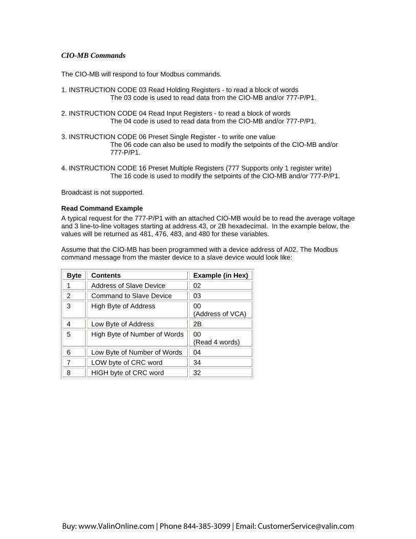
CIO-MB Commands The CIO-MB will respond to four Modbus commands. 1. INSTRUCTION CODE 03 Read Holding Registers - to read a block of words The 03 code is used to read data from the CIO-MB and/or 777-P/P1. 2. INSTRUCTION CODE 04 Read Input Registers - to read a block of words The 04 code is used to read data from the CIO-MB and/or 777-P/P1. 3. INSTRUCTION CODE 06 Preset Single Register - to write one value
The 06 code can also be used to modify the setpoints of the CIO-MB and/or 777-P/P1.
4. INSTRUCTION CODE 16 Preset Multiple Registers (777 Supports only 1 register write) The 16 code is used to modify the setpoints of the CIO-MB and/or 777-P/P1. Broadcast is not supported.
Read Command Example A typical request for the 777-P/P1 with an attached CIO-MB would be to read the average voltage and 3 line-to-line voltages starting at address 43, or 2B hexadecimal. In the example below, the values will be returned as 481, 476, 483, and 480 for these variables. Assume that the CIO-MB has been programmed with a device address of A02. The Modbus command message from the master device to a slave device would look like:
Byte Contents Example (in Hex) 1 Address of Slave Device 02 2 Command to Slave Device 03 3 High Byte of Address 00
(Address of VCA) 4 Low Byte of Address 2B 5 High Byte of Number of Words 00
(Read 4 words) 6 Low Byte of Number of Words 04 7 LOW byte of CRC word 34 8 HIGH byte of CRC word 32
Buy: www.ValinOnline.com | Phone 844-385-3099 | Email: [email protected]
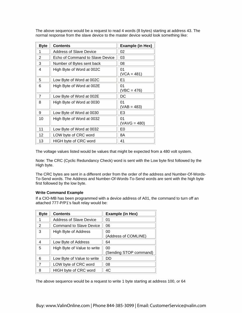
The above sequence would be a request to read 4 words (8 bytes) starting at address 43. The normal response from the slave device to the master device would look something like:
Byte Contents Example (in Hex) 1 Address of Slave Device 02 2 Echo of Command to Slave Device 03 3 Number of Bytes sent back 08 4 High Byte of Word at 002C 01
(VCA = 481) 5 Low Byte of Word at 002C E1 6 High Byte of Word at 002E 01
(VBC = 476) 7 Low Byte of Word at 002E DC 8 High Byte of Word at 0030 01
(VAB = 483) 9 Low Byte of Word at 0030 E3 10 High Byte of Word at 0032 01
(VAVG = 480) 11 Low Byte of Word at 0032 E0 12 LOW byte of CRC word 8A 13 HIGH byte of CRC word 41
The voltage values listed would be values that might be expected from a 480 volt system. Note: The CRC (Cyclic Redundancy Check) word is sent with the Low byte first followed by the High byte. The CRC bytes are sent in a different order from the order of the address and Number-Of-Words-To-Send words. The Address and Number-Of-Words-To-Send words are sent with the high byte first followed by the low byte.
Write Command Example If a CIO-MB has been programmed with a device address of A01, the command to turn off an attached 777-P/P1’s fault relay would be:
Byte Contents Example (in Hex) 1 Address of Slave Device 01 2 Command to Slave Device 06 3 High Byte of Address 00
(Address of COMLINE) 4 Low Byte of Address 64 5 High Byte of Value to write 00
(Sending STOP command) 6 Low Byte of Value to write DD 7 LOW byte of CRC word 08 8 HIGH byte of CRC word 4C
The above sequence would be a request to write 1 byte starting at address 100, or 64
Buy: www.ValinOnline.com | Phone 844-385-3099 | Email: [email protected]

hexadecimal, which is the address of the command word, COMLINE. Refer to Appendix A – 777-P/P1 Modbus Memory Maps for more information about 777-P/P1 commands. The normal response from the CIO-MB is an echo of the same byte sequence back to the master device. This is a confirmation that the command was properly executed.
CRC Testing CRC calculations may be verified by generating the above STOP command and comparing the generated CRC bytes with the CRC bytes listed above. Sending the above command string should result in the 777-P/P1’s display showing “oFF”. The 777-P/P1 will ONLY respond correctly if the CRC bytes, along with the first six bytes, are identical to the above sequence. Invalid CRC bytes received by the 777-P/P1 will result in a communication error and the 777-P/P1 will NOT turn off its relay. NOTE: If an oscilloscope is used to capture the sequence of bits that are being transmitted, note that the MODBUS RTU mode specifies that the LEAST significant bit of each byte is transmitted first. The sequence above would begin with a start bit, followed by the bit sequence: high, low, low, low, low, low, low, low, parity, stop for the first byte (01 hex) sent.
Buy: www.ValinOnline.com | Phone 844-385-3099 | Email: [email protected]

Similarly, the command to reset a 777-P/P1 with an attached CIO-MB would be:
Byte Contents Example (in Hex) 1 Address of Slave Device 01 2 Command to Slave Device 06 3 High Byte of Address 00
(Address of COMLINE) 4 Low Byte of Address 64 5 High Byte of Value to write 00
(Sending RESET command) 6 Low Byte of Value to write AA 7 LOW byte of CRC word 48 8 HIGH byte of CRC word 6A
Number of Write Operations The setpoints in the CIO-MB and 777-P/P1 are stored in non-volatile memory, meaning there are a finite number of writes allowed before the memory is unable to store new values. SymCom recommends that no more than 100,000 writes be performed on non-volatile memory locations. The CIO-MB and 777-P/P1 setpoints can be read indefinitely without degradation of the non-volatile memory.
Special Notes When Using the 4X Addresses Some software packages, such as Human-Machine-Interface (HMI) software packages for PLCs, can only utilize the registers from 400001 to 465536 in the Modbus 03 and 06 commands. If this is the case, add 400001 to the addresses in the tables to select the start of the data to read. Many of these software packages will automatically subtract the 400001 from the address before sending the actual address in the Modbus command. CIO-MB Modbus Memory Map Table 1 - CIO-MB Modbus Memory Map
16 Bit Modbus Address Hex Dec Modicon
R/W Lower Limit
Upper Limit Description Notes
0x2400 9216 49217 R N/A N/A Device Status Bits Bit 0: Trip status Bit 1: Warning status Bit 2: Output A logic Bit 3: Output B logic Bit 4: Input 1 logic Bit 5: Input 2 logic Bit 6: Input 3 logic Bit 7: Input 4 logic Bit 8: Remote reset status Bit 9: CIO-Overload Comm. Watchdog Trip Bit 10: Network-CIO Comm. Watchdog Trip Bit 11: CIO-Overload Comm. Status
0x2401 9217 49218 R N/A N/A Software Revision The revision of the software in the CIO-MB
0x2402 9218 49219 R N/A N/A Product Identifier Product ID of the CIO • CIO-MB = 3000 • CIO-EN = 3100
0x2403 9219 49220 R N/A N/A 777-P Average Current
Raw current read from the overload multiplied by 10
0x2404 9220 49221 R N/A N/A 777-P L1 Current Raw current read from the overload multiplied by 10
0x2405 9221 49222 R N/A N/A 777-P L2 Current Raw current read from the overload multiplied by 10
0x2406 9222 49223 R N/A N/A 777-P L3 Current Raw current read from the overload multiplied by 10
0x2407 9223 49224 R N/A N/A 777-P Ground Fault Current
Raw current read from the overload multiplied by 10
0x2412 9234 49235 R/W 0 3 Digital Output Control Bits
Bit 0: Output A Bit 1: Output B
Buy: www.ValinOnline.com | Phone 844-385-3099 | Email: [email protected]
16 Bit Modbus Address Hex Dec Modicon
R/W Lower Limit
Upper Limit Description Notes
0x2413 9235 49236 R/W 0 7 Digital Output 'On' Control Bits
Setting any of the following bits will turn the corresponding output 'On' without affecting the state of the other outputs. Bit 0: 1 = Output A On Bit 1: 1 = Output B On Bit 2: 1 = Reset Fault Relay
0x2414 9236 49237 R/W 0 7 Digital Output 'Off' Control Bits
Setting any of the following bits will turn the corresponding output 'Off' without affecting the state of the other outputs. Bit 0: 1 = Output A Off Bit 1: 1 = Output B Off Bit 2: 1 = Turn off Fault Relay
0x2415 9237 49238 R/W 0 1023 Network communication configuration bits
Bit 0: 1 = Parity is transmitted (Network-CIO) Bit 1: 1 = Even Parity, 0 = Odd Parity (Network-CIO) Bit 2: 1 = 19200 Baud, 0 = 9600 Baud (Network-CIO) With High Baud Range Enabled, 1 = 57600 Baud, 0 = 38400 Baud Bit 3: 1 = High Baud Range Select Bit 4: 1 = Front Porch Enabled Bit 5: 1 = Back Porch Enabled Bit 6: 1 = Parity is transmitted (CIO-Overload) Bit 7: 1 = Even Parity, 0 = Odd Parity (CIO-Overload) Bit 8: 1 = 19200 Baud, 0 = 9600 Baud (CIO-Overload) Bit 9: 1 = Modbus-RTU Flex Addressing Enabled
0x2416 9238 49239 R/W 0 65535 Back Porch Time Back porch time delay (For advanced users only)
0x2417 9239 49240 R/W 0 65535 Front Porch Time Front porch time delay (For advanced users only)
0x2418 9240 49241 R/W 1 255 Network Modbus address
Modbus address of the CIO (default = 1)
0x2419 9241 49242 R/W 1 255 Back Door address Back door Modbus address of the CIO (default = 127)
0x241A 9242 49243 R/W 1 255 Overload Modbus address
Modbus address of attached 777-P/P1 (default = 1)
0x241B 9243 49244 R/W 0 3 Output invert control bits
Bit 0: 1 = Invert Output A operation Bit 1: 1 = Invert Output B operation
0x241C 9244 49245 R/W 0 3 Output A control functionality
0 = Value set over network only 1 = Value set by link to fault status 2 = Value set by link to warning status 3 = Value set by logic block
0x241D 9245 49246 R/W 0 3 Output B control functionality
0 = Value set over network only 1 = Value set by link to fault status 2 = Value set by link to warning status 3 = Value set by logic block
0x241E 9246 49247 R/W 0 3 Input 1 control functionality
0 = Report value only 1 = Use as remote reset 2 = Use as remote trip 3 = Use as inhibit setting for 777-P
0x241F 9247 49248 R/W 0 2 Input 2 control functionality
0 = Report value only 1 = Use as remote reset 2 = Use as remote trip
0x2420 9248 49249 R/W 0 2 Input 3 control functionality
0 = Report value only 1 = Use as remote reset 2 = Use as remote trip
0x2421 9249 49250 R/W 0 2 Input 4 control functionality
0 = Report value only 1 = Use as remote reset 2 = Use as remote trip
0x2422 9250 49251 R/W 0 2 Remote reset control functionality
0 = Use as remote reset 1 = Use as general input only (report value only) 2 = Use as remote trip
0x2423 9251 49252 R/W 0 65535 Fault Link Mask A Fault link mask for Output A
0x2424 9252 49253 R/W 0 65535 Fault Link Mask B Fault link mask for Output B
0x2425 9253 49254 R/W 0 65535 Warning Link Mask A
Warning link mask for Output A
0x2426 9254 49255 R/W 0 65535 Warning Link Mask B
Warning link mask for Output B
0x2427 9255 49256 R/W 0 31 Logic Block ‘OR’ Mask A
Output A ‘OR’ Mask Bit 0: Input 1 Bit 1: Input 2 Bit 2: Input 3 Bit 3: Input 4 Bit 4: Remote Reset Input
0x2428 9256 49257 R/W 0 31 Logic Block ‘OR’ Mask B
Output B ‘OR’ Mask Bit 0: Input 1 Bit 1: Input 2 Bit 2: Input 3 Bit 3: Input 4 Bit 4: Remote Reset Input
0x2429 9257 49258 R/W 0 31 Logic Block ‘AND’ Mask A
Output A ‘AND’ Mask Bit 0: Input 1 Bit 1: Input 2
Buy: www.ValinOnline.com | Phone 844-385-3099 | Email: [email protected]

16 Bit Modbus Address Hex Dec Modicon
R/W Lower Limit
Upper Limit Description Notes
Bit 2: Input 3 Bit 3: Input 4 Bit 4: Remote Reset Input
0x242A 9258 49259 R/W 0 31 Logic Block ‘AND’ Mask B
Output B ‘AND’ Mask Bit 0: Input 1 Bit 1: Input 2 Bit 2: Input 3 Bit 3: Input 4 Bit 4: Remote Reset Input
0x242B 9259 49260 R/W 0 31 Logic Block ‘NOR’ Mask A
Output A ‘NOR’ Mask Bit 0: Input 1 Bit 1: Input 2 Bit 2: Input 3 Bit 3: Input 4 Bit 4: Remote Reset Input
0x242C 9260 49261 R/W 0 31 Logic Block ‘NOR’ Mask B
Output B ‘NOR’ Mask Bit 0: Input 1 Bit 1: Input 2 Bit 2: Input 3 Bit 3: Input 4 Bit 4: Remote Reset Input
0x242D 9261 49262 R/W 0 31 Logic Block ‘NAND’ Mask A
Output A ‘NAND’ Mask Bit 0: Input 1 Bit 1: Input 2 Bit 2: Input 3 Bit 3: Input 4 Bit 4: Remote Reset Input
0x242E 9262 49263 R/W 0 31 Logic Block ‘NAND’ Mask B
Output B ‘NAND’ Mask Bit 0: Input 1 Bit 1: Input 2 Bit 2: Input 3 Bit 3: Input 4 Bit 4: Remote Reset Input
0x242F 9263 49264 R/W 0 15 Logic Block ‘CMB’ Mask A
Output A ‘CMB’ Mask Bit 0: OR Bit 1: NOR Bit 2: AND Bit 3: NAND Combines logic functions
0x2430 9264 49265 R/W 0 15 Logic Block ‘CMB’ Mask B
Output B ‘CMB’ Mask Bit 0: OR Bit 1: NOR Bit 2: AND Bit 3: NAND Combines logic functions
0x2431 9265 49266 R/W 0 65535 Inhibit Mask 777-P Inhibit mask for Input 1
0x2432 9266 49267 W 0 7 CIO Configuration Bits
Bit 0: 1 = Reset settings to defaults Bit 1: 1 = Reset min/max values2 Bit 2: 1 = Reset file system2
0x2433 9267 49268 R/W 0 63 Watchdog Trip Control Bits
Bit 0: 1 = Network-CIO Comm. restored, send START command to overload Bit 1: 1 = Network-CIO Comm. watchdog, send OFF command to overload Bit 2: 1 = Network-CIO Comm. watchdog, turn off Output B Bit 3: 1 = Network-CIO Comm. watchdog, turn off Output A Bit 4: 1 = CIO-Overload Comm. watchdog, turn off Output B Bit 5: 1 = CIO-Overload Comm. watchdog, turn off Output A
0x2434 9268 49269 R/W 0 15 Real-time Storage Block Configuration
Bit 0: 1 = Real-time Block 1 stored in CIO-MB RAM Bit 1: 1 = Real-time Block 2 stored in CIO-MB RAM Bit 2: 1 = Real-time Block 3 stored in CIO-MB RAM Bit 3: 1 = Real-time Block 4 stored in CIO-MB RAM Storing real-time data from an attached overload in the RAM of the CIO-MB decreases latency in upstream Modbus requests.
0x2435 9269 49270 R/W 0 65535 Real-time Block 1 Start Address
The starting Modbus address at which real-time block 1 requests data from an attached overload
0x2436 9270 49271 R/W 0 30 Real-time Block 1 Number of Words
The number of words that are requested for storage in real-time block 1
0x2437 9271 49272 R/W 0 65535 Real-time Block 2 Start Address
The starting Modbus address at which real-time block 2 requests data from an attached overload
0x2438 9272 49273 R/W 0 30 Real-time Block 2 Number of Words
The number of words that are requested for storage in real-time block 2
0x2439 9273 49274 R/W 0 65535 Real-time Block 3 Start Address
The starting Modbus address at which real-time block 3 requests data from an attached overload
Buy: www.ValinOnline.com | Phone 844-385-3099 | Email: [email protected]

16 Bit Modbus Address Hex Dec Modicon
R/W Lower Limit
Upper Limit Description Notes
0x243A 9274 49275 R/W 0 30 Real-time Block 3 Number of Words
The number of words that are requested for storage in real-time block 3
0x243B 9275 49276 R/W 0 65535 Real-time Block 4 Start Address
The starting Modbus address at which real-time block 4 requests data from an attached overload
0x243C 9276 49277 R/W 0 30 Real-time Block 4 Number of Words
The number of words that are requested for storage in real-time block 4
0x243D 9277 49278 R/W 0 15 Limit Storage Block Configuration
Bit 0: 1 = Limit Block 1 stored in CIO-MB RAM Bit 1: 1 = Limit Block 2 stored in CIO-MB RAM Bit 2: 1 = Limit Block 3 stored in CIO-MB RAM Bit 3: 1 = Limit Block 4 stored in CIO-MB RAM Storing limit data from an attached overload in the RAM of the CIO-MB decreases latency in upstream Modbus requests.
0x243E 9278 49279 R/W 0 65535 Limit Block 1 Start Address
The starting Modbus address at which limit block 1 requests data from an attached overload
0x243F 9279 49280 R/W 0 30 Limit Block 1 Number of Words
The number of words that are requested for storage in limit block 1
0x2440 9280 49281 R/W 0 65535 Limit Block 2 Start Address
The starting Modbus address at which limit block 2 requests data from an attached overload
0x2441 9281 49282 R/W 0 30 Limit Block 2 Number of Words
The number of words that are requested for storage in limit block 2
0x2442 9282 49283 R/W 0 65535 Limit Block 3 Start Address
The starting Modbus address at which limit block 3 requests data from an attached overload
0x2443 9283 49284 R/W 0 30 Limit Block 3 Number of Words
The number of words that are requested for storage in limit block 3
0x2444 9284 49285 R/W 0 65535 Limit Block 4 Start Address
The starting Modbus address at which limit block 4 requests data from an attached overload
0x2445 9285 49286 R/W 0 30 Limit Block 4 Number of Words
The number of words that are requested for storage in limit block 4
0x2446 9286 49287 R/W 0 65535 Fault Register Modbus Address
The Modbus address of the register that contains the attached overload fault status (777-P/P1 Default = 0x0006 Trip Reason)
0x2447 9287 49288 R/W 0 65535 Pending Fault Register Modbus Address
The Modbus address of the register that contains the attached overload pending fault status (777-P/P1 Default = 0x0005 Overload Status)
0x2448 9288 49289 R/W 0 65535 Warning Status Register Modbus Address
The Modbus address of the register that contains the attached overload warning status (777-P/P1 Default = 0x001C Warning Status)
0x2449 9289 49290 R/W 0 65535 Command Line Register Modbus Address
The Modbus address of the register that is used for start/stop commands in the overload (777-P/P1 Default = 0x0064 Command Line)
0x244A 9290 49291 R/W 0 65535 Command Line – Start Command
The START command sent to an overload via the command line (777-P/P1 Default = 0x00AA)
0x244B 9291 49292 R/W 0 65535 Command Line – Stop Command
The STOP command sent to an overload via the command line (777-P/P1 Default = 0x00DD)
0x2478 9336 49337 R/W 0 65535 Modbus Assembly 502 Parameter 1
Modbus register to access in Modbus Assembly 502
0x2479 9337 49338 R/W 0 65535 Modbus Assembly 502 Parameter 2
Modbus register to access in Modbus Assembly 502
0x247A 9338 49339 R/W 0 65535 Modbus Assembly 502 Parameter 3
Modbus register to access in Modbus Assembly 502
0x247B 9339 49340 R/W 0 65535 Modbus Assembly 502 Parameter 4
Modbus register to access in Modbus Assembly 502
0x247C 9340 49341 R/W 0 65535 Modbus Assembly 502 Parameter 5
Modbus register to access in Modbus Assembly 502
0x247D 9341 49342 R/W 0 65535 Modbus Assembly 502 Parameter 6
Modbus register to access in Modbus Assembly 502
0x247E 9342 49343 R/W 0 65535 Modbus Assembly 502 Parameter 7
Modbus register to access in Modbus Assembly 502
0x247F 9343 49344 R/W 0 65535 Modbus Assembly 502 Parameter 8
Modbus register to access in Modbus Assembly 502
0x2480 9344 49345 R/W 0 65535 Modbus Assembly 502 Parameter 9
Modbus register to access in Modbus Assembly 502
0x2481 9345 49346 R/W 0 65535 Modbus Assembly 502 Parameter 10
Modbus register to access in Modbus Assembly 502
0x2482 9346 49347 R/W 0 65535 Modbus Assembly 502 Parameter 11
Modbus register to access in Modbus Assembly 502
0x2483 9347 49348 R/W 0 65535 Modbus Assembly 502 Parameter 12
Modbus register to access in Modbus Assembly 502
0x2484 9348 49349 R/W 0 65535 Modbus Assembly 502 Parameter 13
Modbus register to access in Modbus Assembly 502
Buy: www.ValinOnline.com | Phone 844-385-3099 | Email: [email protected]
16 Bit Modbus Address Hex Dec Modicon
R/W Lower Limit
Upper Limit Description Notes
0x2485 9349 49350 R/W 0 65535 Modbus Assembly 502 Parameter 14
Modbus register to access in Modbus Assembly 502
0x2486 9350 49351 R/W 0 65535 Modbus Assembly 502 Parameter 15
Modbus register to access in Modbus Assembly 502
0x2487 9351 49352 R/W 0 65535 Modbus Assembly 502 Parameter 16
Modbus register to access in Modbus Assembly 502
0x2488 9352 49353 R/W 0 65535 Modbus Assembly 502 Parameter 17
Modbus register to access in Modbus Assembly 502
0x2489 9353 49354 R/W 0 65535 Modbus Assembly 502 Parameter 18
Modbus register to access in Modbus Assembly 502
0x248A 9354 49355 R/W 0 65535 Modbus Assembly 502 Parameter 19
Modbus register to access in Modbus Assembly 502
0x248B 9355 49356 R/W 0 65535 Modbus Assembly 502 Parameter 20
Modbus register to access in Modbus Assembly 502
0x248C 9356 49357 R/W 0 65535 Modbus Assembly 502 Parameter 21
Modbus register to access in Modbus Assembly 502
0x248D 9357 49358 R/W 0 65535 Modbus Assembly 502 Parameter 22
Modbus register to access in Modbus Assembly 502
0x248E 9358 49359 R/W 0 65535 Modbus Assembly 502 Parameter 23
Modbus register to access in Modbus Assembly 502
0x248F 9359 49360 R/W 0 65535 Modbus Assembly 502 Parameter 24
Modbus register to access in Modbus Assembly 502
0x2490 9360 49361 R/W 0 65535 Modbus Assembly 502 Parameter 25
Modbus register to access in Modbus Assembly 502
0x2491 9361 49362 R/W 0 65535 Modbus Assembly 502 Parameter 26
Modbus register to access in Modbus Assembly 502
0x2492 9362 49363 R/W 0 65535 Modbus Assembly 502 Parameter 27
Modbus register to access in Modbus Assembly 502
0x2493 9363 49364 R/W 0 65535 Modbus Assembly 502 Parameter 28
Modbus register to access in Modbus Assembly 502
0x2494 9364 49365 R/W 0 65535 Modbus Assembly 502 Parameter 29
Modbus register to access in Modbus Assembly 502
0x2495 9365 49366 R/W 0 65535 Modbus Assembly 502 Parameter 30
Modbus register to access in Modbus Assembly 502
0x2496 9366 49367 R/W 0 65535 Modbus Assembly 502 Parameter 31
Modbus register to access in Modbus Assembly 502
0x2497 9367 49368 R/W 0 65535 Modbus Assembly 502 Parameter 32
Modbus register to access in Modbus Assembly 502
0x2498 9368 49369 R/W 0 65535 Modbus Assembly 502 Parameter 33
Modbus register to access in Modbus Assembly 502
0x2499 9369 49370 R/W 0 65535 Modbus Assembly 502 Parameter 34
Modbus register to access in Modbus Assembly 502
0x249A 9370 49371 R/W 0 65535 Modbus Assembly 502 Parameter 35
Modbus register to access in Modbus Assembly 502
0x249B 9371 49372 R/W 0 65535 Modbus Assembly 502 Parameter 36
Modbus register to access in Modbus Assembly 502
0x249C 9372 49373 R/W 0 65535 Modbus Assembly 502 Parameter 37
Modbus register to access in Modbus Assembly 502
0x249D 9373 49374 R/W 0 65535 Modbus Assembly 502 Parameter 38
Modbus register to access in Modbus Assembly 502
0x249E 9374 49375 R/W 0 65535 Modbus Assembly 502 Parameter 39
Modbus register to access in Modbus Assembly 502
0x249F 9375 49376 R/W 0 65535 Modbus Assembly 502 Parameter 40
Modbus register to access in Modbus Assembly 502
Notes: 1 May not be available in all models 2 Reserved for future use
Buy: www.ValinOnline.com | Phone 844-385-3099 | Email: [email protected]

Real-time Values
Device Status Bits The device status bits display status information about the CIO-MB and an attached overload (if applicable). Table 2 defines each bit in the device status register. Table 2 - Network Communication Configuration Bits
Bit Name Description 0 Trip status 1 = an attached overload has tripped due to a fault 1 Warning status 1 = an attached overload has a warning 2 Output A logic 0 = Output A is opened
1 = Output A is closed 3 Output B logic 0 = Output B is opened
1 = Output B is closed 4 Input 1 logic 0 = Input 1 is off
1 = Input 1 is on 5 Input 2 logic 0 = Input 2 is off
1 = Input 2 is on 6 Input 3 logic 0 = Input 3 is off
1 = Input 3 is on 7 Input 4 logic 0 = Input 4 is off
1 = Input 4 is on 8 Remote reset
status 0 = Remote reset input is off 1 = Remote reset input is on
9 CIO-Overload comm. watchdog trip
1 = A 5 second communications watchdog has occurred between the CIO and attached overload
10 Network-CIO comm. watchdog trip
1 = A 5 second communications watchdog has occurred between the CIO and an upstream device
11 CIO-Overload comm. status
1 = The CIO is successfully communicating with an attached overload
Overload Currents The CIO-MB provides real-time current values read from an attached overload (if applicable) that are always scaled by 10. This provides current values that are scaled by a fixed value, eliminating the need for the user to manually scale the currents by the adjustable scalar native to the overload. As an important note, the overload's scalar and current register addresses must be stored in the real-time configuration blocks (discussed later in this document) in order for them to update correctly.
Buy: www.ValinOnline.com | Phone 844-385-3099 | Email: [email protected]

Network Communication
Network Communication Configuration Bits The network communication configuration bits provide configuration for the CIO-MB serial communication settings. The default values and their descriptions are listed in Table 3. Table 3 - Network Communication Configuration Bits
Bit Default Setting
Description
0 1 1 = a parity bit is expected in Network-CIO communications 1 1 1 = even parity is expected in Network-CIO communications
0 = odd parity is expected in Network-CIO communications Note: Bit 0 must be set to enable Bit 1
2 0 0 = 9600 Baud rate in Network-CIO communications (38400 with High Baud Range enabled) 1 = 19200 Baud rate in Network-CIO communications (57600 with High Baud Range enabled)
3 0 0 = High Baud Range Disabled 1 = High Baud Range Enabled
4 1 1 = Network-CIO communications front porch enabled (linked to front porch time setting)
5 1 1 = Network-CIO communications back porch enabled (linked to back porch time setting)
6 1 1 = a parity bit is transmitted in CIO-Overload communications 7 1 1 = even parity is transmitted in CIO-Overload communications
0 = odd parity is transmitted in CIO-Overload communications Note: Bit 5 must be set to enable Bit 6
8 0 0 = 9600 Baud rate in CIO-Overload communications 1 = 19200 Baud rate in CIO-Overload communications
9 1 1 = Flexible addressing enabled Note: The settings for the CIO-MB must match the settings for the network and for the overload in order to establish communication. Changing CIO-MB communications settings may affect upstream and/or downstream communications.
Flexible Addressing By default, flexible addressing is enabled in the CIO-MB. This means that the address of the CIO-MB will always automatically match the Modbus address of an attached overload. Disabling flexible addressing could result in the CIO-MB and attached overload having different Modbus addresses.
Front/Back Porch Times A communications front porch is simply a method of biasing a communications signal before actually transmitting a message. Biasing the communications signal provides the intended receiver with an indication that a message is being sent; this allows the receiver time to prepare for message reception. A back porch works in a similar fashion, signaling the end of a message. The front and back porch time settings represent character times as opposed to actual time values, and should not be changed unless required.
Buy: www.ValinOnline.com | Phone 844-385-3099 | Email: [email protected]
I/O Functionality
Digital Output Control The states of the output relays can be changed at any time from a Modbus master. Bit 0 provides network control over Output A and bit 1 provides network control over Output B. Setting a bit will turn on an output relay whereas clearing a bit will turn off an output relay. As an important note, network control is overridden when outputs are linked to logic, fault status, or warning status.
Digital Output 'On' Control The digital output 'on' control register provides the ability to turn on an output relay without affecting the state of the other outputs. Bit 0 provides network control over Output A, bit 1 provides network control over Output B, and bit 2 provides network control over an attached 777-P/P1. As an important note, network control is overridden when outputs are linked to logic, fault status, or warning status.
Digital Output 'Off' Control The digital output 'off' control register provides the ability to turn off an output relay without affecting the state of the other outputs. Bit 0 provides network control over Output A, bit 1 provides network control over Output B, and bit 2 provides network control over an attached 777-P/P1. As an important note, network control is overridden when outputs are linked to logic, fault status, or warning status.
Output Invert Control Bits The output invert control register provides the ability to invert the logic of the output relays. Setting bit 0 inverts the logic of output A and setting bit 1 inverts the logic of output B.
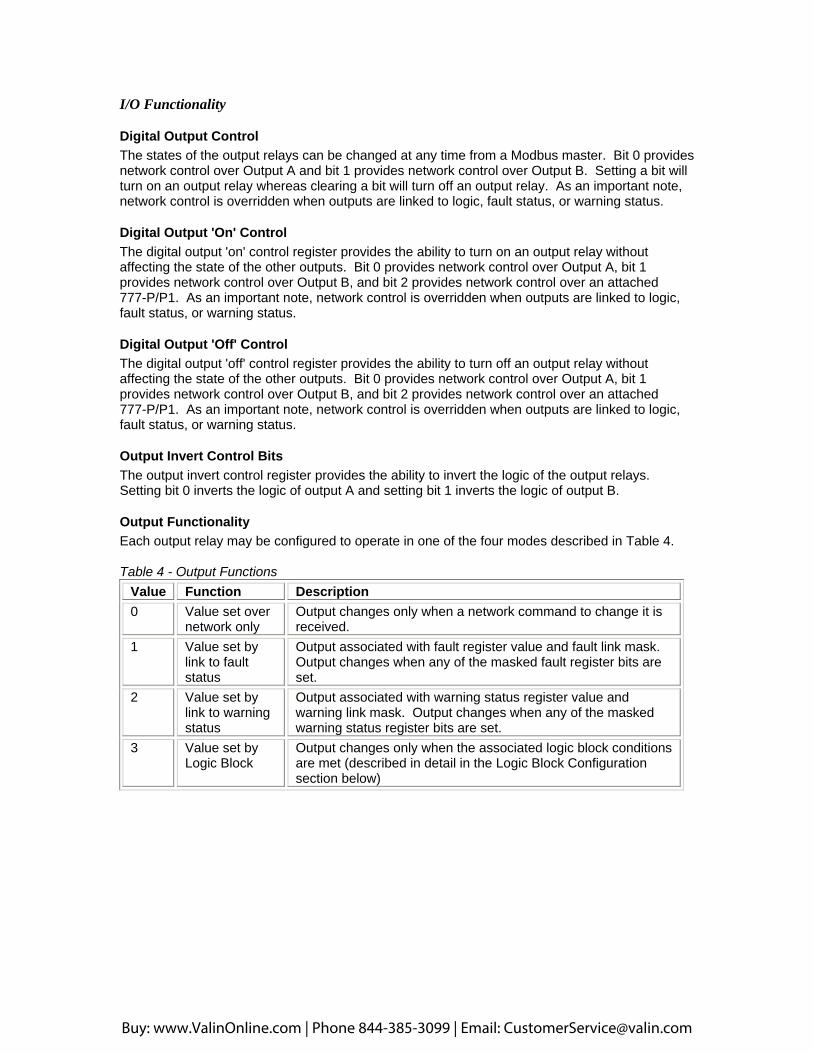
Output Functionality Each output relay may be configured to operate in one of the four modes described in Table 4. Table 4 - Output Functions
Value Function Description 0 Value set over
network only Output changes only when a network command to change it is received.
1 Value set by link to fault status
Output associated with fault register value and fault link mask. Output changes when any of the masked fault register bits are set.
2 Value set by link to warning status
Output associated with warning status register value and warning link mask. Output changes when any of the masked warning status register bits are set.
3 Value set by Logic Block
Output changes only when the associated logic block conditions are met (described in detail in the Logic Block Configuration section below)
Buy: www.ValinOnline.com | Phone 844-385-3099 | Email: [email protected]
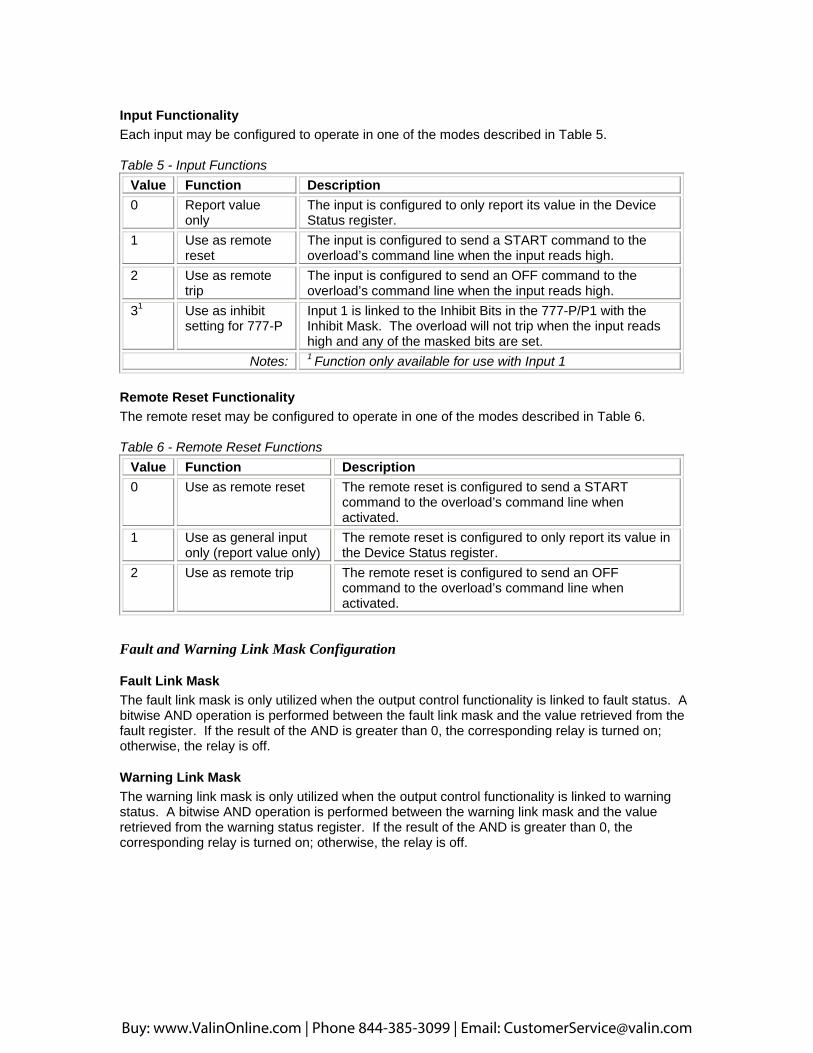
Input Functionality Each input may be configured to operate in one of the modes described in Table 5. Table 5 - Input Functions
Value Function Description 0 Report value
only The input is configured to only report its value in the Device Status register.
1 Use as remote reset
The input is configured to send a START command to the overload’s command line when the input reads high.
2 Use as remote trip
The input is configured to send an OFF command to the overload’s command line when the input reads high.
31 Use as inhibit setting for 777-P
Input 1 is linked to the Inhibit Bits in the 777-P/P1 with the Inhibit Mask. The overload will not trip when the input reads high and any of the masked bits are set.
Notes: 1 Function only available for use with Input 1
Remote Reset Functionality The remote reset may be configured to operate in one of the modes described in Table 6. Table 6 - Remote Reset Functions
Value Function Description 0 Use as remote reset The remote reset is configured to send a START
command to the overload’s command line when activated.
1 Use as general input only (report value only)
The remote reset is configured to only report its value in the Device Status register.
2 Use as remote trip The remote reset is configured to send an OFF command to the overload’s command line when activated.
Fault and Warning Link Mask Configuration
Fault Link Mask The fault link mask is only utilized when the output control functionality is linked to fault status. A bitwise AND operation is performed between the fault link mask and the value retrieved from the fault register. If the result of the AND is greater than 0, the corresponding relay is turned on; otherwise, the relay is off.
Warning Link Mask The warning link mask is only utilized when the output control functionality is linked to warning status. A bitwise AND operation is performed between the warning link mask and the value retrieved from the warning status register. If the result of the AND is greater than 0, the corresponding relay is turned on; otherwise, the relay is off.
Buy: www.ValinOnline.com | Phone 844-385-3099 | Email: [email protected]

Logic Block Configuration
Setting for Logic Block OR mask If all bits are ZERO, the OR function is ignored (OR function value is 0). If any bit is set to 1 and the corresponding input pin reads high, the OR function value is 1. Table 7 - Logic Block OR
Bit Number Associated Input Bit 0 Input 1 Bit 1 Input 2 Bit 2 Input 3 Bit 3 Input 4 Bit 4 Remote Reset Input
Setting for Logic Block NOR mask If all bits are ZERO, the NOR function is ignored (NOR function value is 0). If any bit is set to 1 and the corresponding COMPLEMENTED input pin reads high, (i.e. the input pin itself reads low) the NOR function value is 1.
Table 8 - Logic Block NOR
Bit Number Associated Input Bit 0 Input 1 Bit 1 Input 2 Bit 2 Input 3 Bit 3 Input 4 Bit 4 Remote Reset Input
Setting for Logic Block AND mask If all bits are ZERO, the AND function is ignored (AND function value is 0). If all bits that are set to 1 match the value (high) of the corresponding input pins, the AND function value is 1.
Table 9 - Logic Block AND
Bit Number Associated Input Bit 0 Input 1 Bit 1 Input 2 Bit 2 Input 3 Bit 3 Input 4 Bit 4 Remote Reset Input
Buy: www.ValinOnline.com | Phone 844-385-3099 | Email: [email protected]

Setting for Logic Block NAND mask If all bits are ZERO, the NAND function is ignored (NAND function value is 0). If all bits that are set to 1 match the value (high) of the corresponding COMPLEMENTED input pins, the NAND function value is 1.
Table 10 – Logic Block NAND
Bit Number Associated Input Bit 0 Input 1 Bit 1 Input 2 Bit 2 Input 3 Bit 3 Input 4 Bit 4 Remote Reset Input
Setting for Logic Block COMBINATION mask If any bit is ZERO, the corresponding outputs of the logic blocks are OR'ed together. If the result is high, the COMBINATION function value is 1. If all bits that are set to 1 match the value (high) of the corresponding logic block, the COMBINATION function value is 1.
Table 11 – Logic Block CMB
Bit Number Associated Logic Operation Bit 0 OR function Bit 1 NOR function Bit 2 AND function Bit 3 NAND function
Inhibit Mask Configuration
Inhibit Mask The inhibit mask is used only when Input 1 control functionality is set to “Use as inhibit setting for 777-P”. The inhibit mask is directly linked to the 777-P/P1’s Inhibit Bits register. Setting any of the mask bits high enables Input 1 to inhibit the overload from tripping on that corresponding fault. CIO Configuration
Reset settings to defaults Setting bit 0 will reset all CIO-MB limit/setpoint data to factory default values. Note: Setting this bit will erase all existing CIO-MB settings!
Buy: www.ValinOnline.com | Phone 844-385-3099 | Email: [email protected]

Watchdog Trip Control Configuration
Watchdog Trip Control Bits The functionality of the watchdog trip control bits is described in Table 12. Table 12 – Watchdog Trip Control Bits
Bit Function Description 0 Network-CIO Comm. restored, send
START command to overload The CIO-MB will send a START command to the attached overload when communication is reestablished over the network.
1 Network-CIO Comm. watchdog, send OFF command to overload
The CIO-MB will send an OFF command to the attached overload when communication is lost over the network.
2 Network-CIO Comm. watchdog, turn off Output B
The CIO-MB will turn off Output B when communication has been lost over the network for at least 5 seconds.
3 Network-CIO Comm. watchdog, turn off Output A
The CIO-MB will turn off Output A when communication has been lost over the network for at least 5 seconds.
4 CIO-Overload Comm. watchdog, turn off Output B
The CIO-MB will turn off Output B when communication has been lost with the overload for at least 5 seconds.
5 CIO-Overload Comm. watchdog, turn off Output A
The CIO-MB will turn off Output A when communication has been lost with the overload for at least 5 seconds.
Storage Block Configuration
Storage Block Configuration Real-time and limit/setpoint data from an attached overload may be stored in the CIO-MB’s RAM to minimize Modbus response latency. Modbus messages that require data from the overload not stored in the CIO-MB’s RAM must be passed through the overload, increasing the response time. The CIO-MB provides four 30-word RAM blocks dedicated to real-time data and four 30-word RAM blocks dedicated to limit/setpoint data. Each block has an associated Modbus starting address and number of words to be read from the overload. Table 13 describes the storage block configuration bits for both the real-time and limit data. Table 13 – Storage Block Configuration Bits
Bit Function Description 0 Block 1 stored in CIO-MB
RAM Setting this bit to a 1 will store all the values corresponding to the addresses configured in block 1 to the CIO-MB RAM.
1 Block 2 stored in CIO-MB RAM
Setting this bit to a 1 will store all the values corresponding to the addresses configured in block 2 to the CIO-MB RAM.
2 Block 3 stored in CIO-MB RAM
Setting this bit to a 1 will store all the values corresponding to the addresses configured in block 2 to the CIO-MB RAM.
3 Block 4 stored in CIO-MB RAM
Setting this bit to a 1 will store all the values corresponding to the addresses configured in block 3 to the CIO-MB RAM.
Note: Do not attempt to store any of the CIO-MB’s Modbus addresses in the real-time/limit storage blocks. These blocks are specifically designated to store data from the overload.
Buy: www.ValinOnline.com | Phone 844-385-3099 | Email: [email protected]
Customizable Addresses/Commands
Customizable Addresses The CIO-MB provides the user with a way to customize certain addresses for ease of use. The Fault Register, Warning Status Register, and Command Line Register can all be changed. The default addresses are shown in the CIO-MB Memory Map. Note: These registers should be changed by advanced users only.
Customizable Commands The CIO-MB allows the user to change the commands to stop and start the overload. These commands are linked to the Command Line Register, and the defaults are listed in the CIO-MB Memory Map. Modbus Assembly Parameters
Modbus Assembly 502 Parameter 1-40 The Modbus assembly allows the master to read up to 40 setpoint and real-time data in any order independent of the published memory map. Each Modbus assembly parameter represents a Modbus address, and the value can be read via Modbus register 502. The number of parameters returned in a Modbus 0x03 read is specified by the number of registers read. All overload data must be stored in the CIO-MB’s internal RAM via the real-time/limit storage blocks described above.
Buy: www.ValinOnline.com | Phone 844-385-3099 | Email: [email protected]
Appendix A – 777-P/P1 Modbus Memory Maps
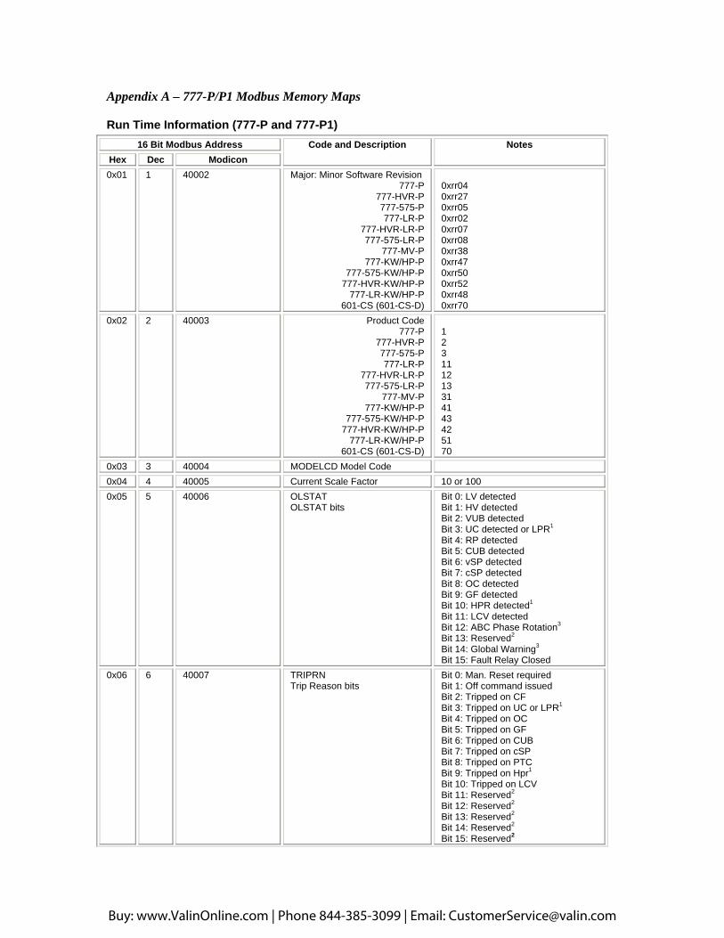
Run Time Information (777-P and 777-P1) 16 Bit Modbus Address
Hex Dec Modicon Code and Description Notes
0x01 1 40002 Major: Minor Software Revision 777-P
777-HVR-P 777-575-P 777-LR-P
777-HVR-LR-P 777-575-LR-P
777-MV-P 777-KW/HP-P
777-575-KW/HP-P 777-HVR-KW/HP-P
777-LR-KW/HP-P 601-CS (601-CS-D)
0xrr04 0xrr27 0xrr05 0xrr02
0xrr07 0xrr08
0xrr38 0xrr47 0xrr50 0xrr52 0xrr48 0xrr70
0x02 2 40003 Product Code 777-P
777-HVR-P 777-575-P 777-LR-P
777-HVR-LR-P 777-575-LR-P
777-MV-P 777-KW/HP-P
777-575-KW/HP-P 777-HVR-KW/HP-P
777-LR-KW/HP-P 601-CS (601-CS-D)
1 2 3 11 12 13 31 41 43 42 51 70
0x03 3 40004 MODELCD Model Code 0x04 4 40005 Current Scale Factor 10 or 100 0x05 5 40006 OLSTAT
OLSTAT bits Bit 0: LV detected Bit 1: HV detected Bit 2: VUB detected Bit 3: UC detected or LPR1
Bit 4: RP detected Bit 5: CUB detected Bit 6: vSP detected Bit 7: cSP detected Bit 8: OC detected Bit 9: GF detected Bit 10: HPR detected1
Bit 11: LCV detected Bit 12: ABC Phase Rotation3
Bit 13: Reserved2
Bit 14: Global Warning3
Bit 15: Fault Relay Closed 0x06 6 40007 TRIPRN
Trip Reason bits Bit 0: Man. Reset required Bit 1: Off command issued Bit 2: Tripped on CF Bit 3: Tripped on UC or LPR1
Bit 4: Tripped on OC Bit 5: Tripped on GF Bit 6: Tripped on CUB Bit 7: Tripped on cSP Bit 8: Tripped on PTC Bit 9: Tripped on Hpr1
Bit 10: Tripped on LCV Bit 11: Reserved2 Bit 12: Reserved2
Bit 13: Reserved2
Bit 14: Reserved2
Bit 15: Reserved2
Buy: www.ValinOnline.com | Phone 844-385-3099 | Email: [email protected]

16 Bit Modbus Address Hex Dec Modicon
Code and Description Notes
0x07 7 40008 LF1 Last Fault
Code Definition 0 Cleared 1 Reserved2
2 Reserved2
4 Contactor Failure 6 Single Phased Current 7 Ground Fault 8 Current Unbalance 9 Reserved2
10 Overcurrent 11 Undercurrent 12 Reserved2
13 Reserved2 14 Reserved2
15 Low Kilowatt Trip (Low Power)1
16 PTC Off 17 High Kilowatt Trip (High Power)1
18 Reserved2 19 Low control voltage trip
0x08 8 40009 LF2 Second to Last Fault
Code Definition 0 Cleared 1 Reserved2
2 Reserved2
4 Contactor Failure 6 Single Phased Current 7 Ground Fault 8 Current Unbalance 9 Reserved2
10 Overcurrent 11 Undercurrent 12 Reserved2
13 Reserved2 14 Reserved2
15 Low Kilowatt Trip (Low Power)1
16 PTC Off 17 High Kilowatt Trip (High Power)1
18 Reserved2 19 Low control voltage trip
0x09 9 40010 LF3 Third to Last Fault
Code Definition 0 Cleared 1 Reserved2
2 Reserved2
4 Contactor Failure 6 Single Phased Current 7 Ground Fault 8 Current Unbalance 9 Reserved2
10 Overcurrent 11 Undercurrent 12 Reserved2
13 Reserved2 14 Reserved2
15 Low Kilowatt Trip (Low Power)1
16 PTC Off 17 High Kilowatt Trip (High Power)1
Buy: www.ValinOnline.com | Phone 844-385-3099 | Email: [email protected]
16 Bit Modbus Address Hex Dec Modicon
Code and Description Notes
18 Reserved2 19 Low control voltage trip
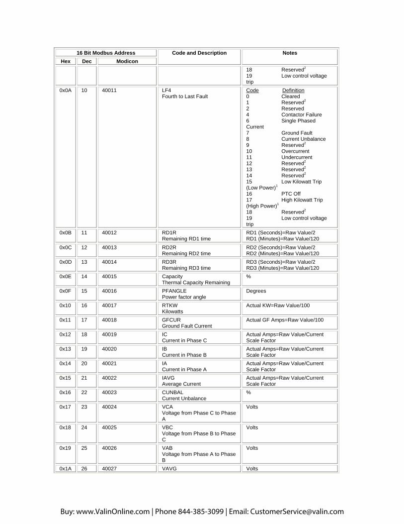
0x0A 10 40011 LF4 Fourth to Last Fault
Code Definition 0 Cleared 1 Reserved2
2 Reserved
4 Contactor Failure 6 Single Phased Current 7 Ground Fault 8 Current Unbalance 9 Reserved2
10 Overcurrent 11 Undercurrent 12 Reserved2
13 Reserved2 14 Reserved2
15 Low Kilowatt Trip (Low Power)1
16 PTC Off 17 High Kilowatt Trip (High Power)1
18 Reserved2 19 Low control voltage trip
0x0B 11 40012 RD1R Remaining RD1 time
RD1 (Seconds)=Raw Value/2 RD1 (Minutes)=Raw Value/120
0x0C 12 40013 RD2R Remaining RD2 time
RD2 (Seconds)=Raw Value/2 RD2 (Minutes)=Raw Value/120
0x0D 13 40014 RD3R Remaining RD3 time
RD3 (Seconds)=Raw Value/2 RD3 (Minutes)=Raw Value/120
0x0E 14 40015 Capacity Thermal Capacity Remaining
%
0x0F 15 40016 PFANGLE Power factor angle
Degrees
0x10 16 40017 RTKW Kilowatts
Actual KW=Raw Value/100
0x11 17 40018 GFCUR Ground Fault Current
Actual GF Amps=Raw Value/100
0x12 18 40019 IC Current in Phase C
Actual Amps=Raw Value/Current Scale Factor
0x13 19 40020 IB Current in Phase B
Actual Amps=Raw Value/Current Scale Factor
0x14 20 40021 IA Current in Phase A
Actual Amps=Raw Value/Current Scale Factor
0x15 21 40022 IAVG Average Current
Actual Amps=Raw Value/Current Scale Factor
0x16 22 40023 CUNBAL Current Unbalance
%
0x17 23 40024 VCA Voltage from Phase C to Phase A
Volts
0x18 24 40025 VBC Voltage from Phase B to Phase C
Volts
0x19 25 40026 VAB Voltage from Phase A to Phase B
Volts
0x1A 26 40027 VAVG Volts
Buy: www.ValinOnline.com | Phone 844-385-3099 | Email: [email protected]
16 Bit Modbus Address Hex Dec Modicon
Code and Description Notes
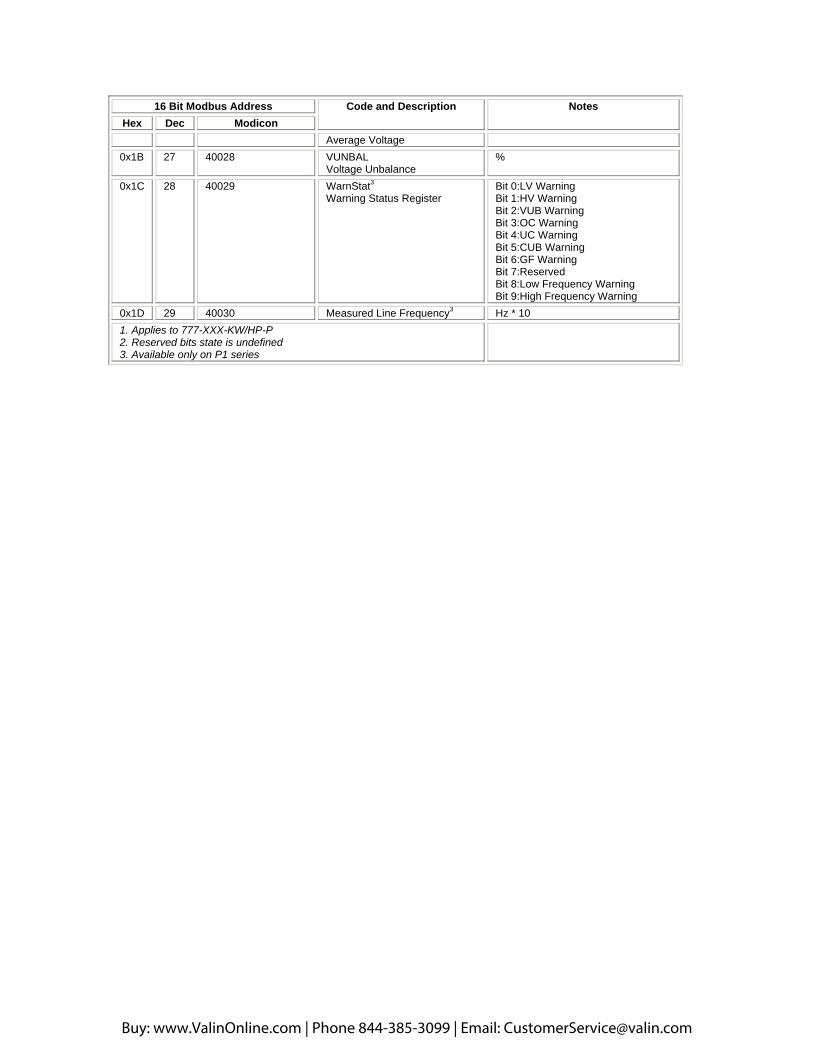
Average Voltage 0x1B 27 40028 VUNBAL
Voltage Unbalance %
0x1C 28 40029 WarnStat3
Warning Status Register Bit 0:LV Warning Bit 1:HV Warning Bit 2:VUB Warning Bit 3:OC Warning Bit 4:UC Warning Bit 5:CUB Warning Bit 6:GF Warning Bit 7:Reserved Bit 8:Low Frequency Warning Bit 9:High Frequency Warning
0x1D 29 40030 Measured Line Frequency3 Hz * 10 1. Applies to 777-XXX-KW/HP-P 2. Reserved bits state is undefined 3. Available only on P1 series
Buy: www.ValinOnline.com | Phone 844-385-3099 | Email: [email protected]
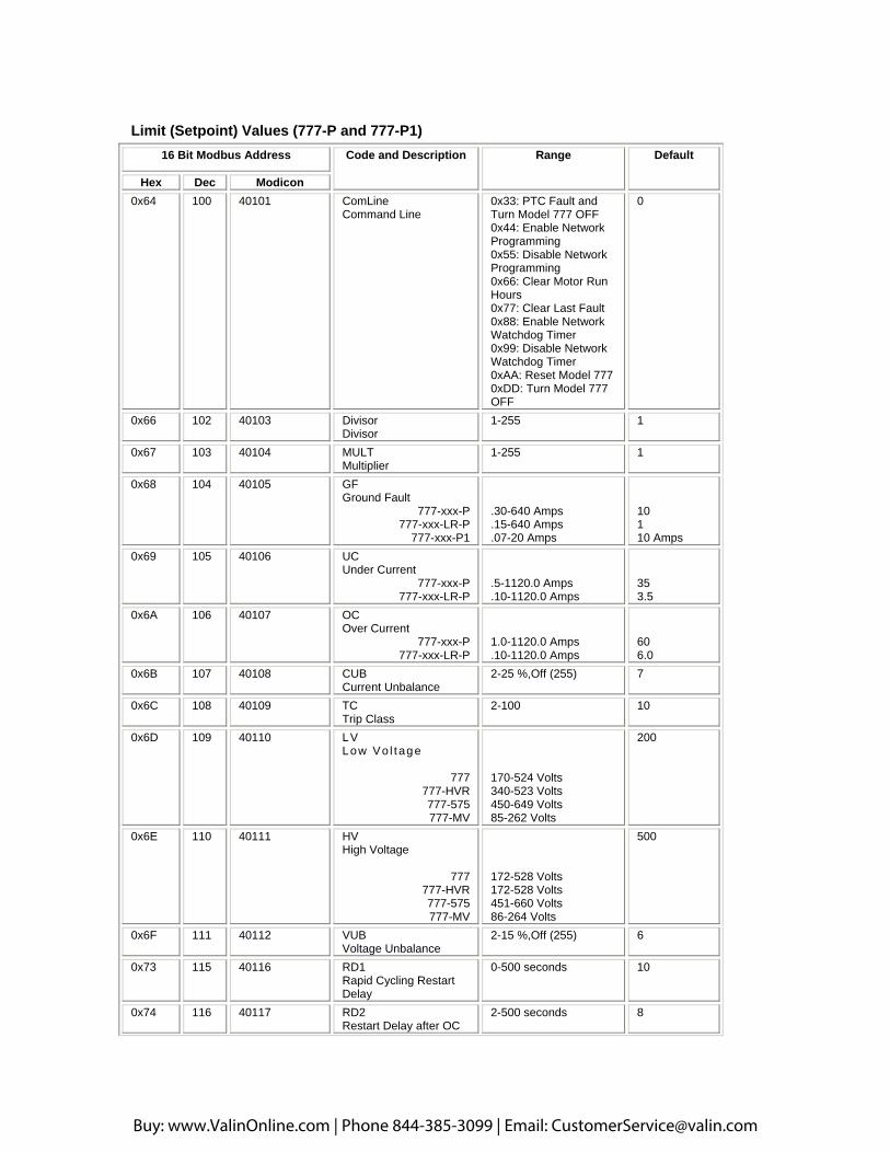
Limit (Setpoint) Values (777-P and 777-P1) 16 Bit Modbus Address
Hex Dec Modicon
Code and Description Range Default
0x64 100 40101 ComLine Command Line
0x33: PTC Fault and Turn Model 777 OFF 0x44: Enable Network Programming 0x55: Disable Network Programming 0x66: Clear Motor Run Hours 0x77: Clear Last Fault 0x88: Enable Network Watchdog Timer 0x99: Disable Network Watchdog Timer 0xAA: Reset Model 777 0xDD: Turn Model 777 OFF
0
0x66 102 40103 Divisor Divisor
1-255 1
0x67 103 40104 MULT Multiplier
1-255 1
0x68 104 40105 GF Ground Fault
777-xxx-P 777-xxx-LR-P
777-xxx-P1
.30-640 Amps .15-640 Amps .07-20 Amps
10 1 10 Amps
0x69 105 40106 UC Under Current
777-xxx-P 777-xxx-LR-P
.5-1120.0 Amps .10-1120.0 Amps
35 3.5
0x6A 106 40107 OC Over Current
777-xxx-P 777-xxx-LR-P
1.0-1120.0 Amps .10-1120.0 Amps
60 6.0
0x6B 107 40108 CUB Current Unbalance
2-25 %,Off (255) 7
0x6C 108 40109 TC Trip Class
2-100 10
0x6D 109 40110 LV Low Vo l tage
777 777-HVR 777-575 777-MV
170-524 Volts 340-523 Volts 450-649 Volts 85-262 Volts
200
0x6E 110 40111 HV High Voltage
777 777-HVR 777-575 777-MV
172-528 Volts 172-528 Volts 451-660 Volts 86-264 Volts
500
0x6F 111 40112 VUB Voltage Unbalance
2-15 %,Off (255) 6
0x73 115 40116 RD1 Rapid Cycling Restart Delay
0-500 seconds 10
0x74 116 40117 RD2 Restart Delay after OC
2-500 seconds 8
Buy: www.ValinOnline.com | Phone 844-385-3099 | Email: [email protected]

fault 0x75 117 40118 RD3
Restart Delay after UC fault
2-500 seconds, A (65535)
20
0x76 118 40119 UCTD Under Current Trip Delay
2-255s 5
0x77 119 40120 #RU Number of restarts after UC fault
0, 1, 2, 3, 4, A (automatic) RU Values 0–4 0–4 A 255
1
0x78 120 40121 #RF Number of restarts after OC,cSP,CUB,LCV,HPR1 fault
0, 1, oc1, 2, oc2, 3, oc3, 4, oc4, A, ocA 0 = manual, A = continuous, oc = automatic restart after RD2 expires RF Value Decimal Value 0 1 1 2 oc1 3 2 4 oc2 5 3 6 oc3 7 4 8 oc4 9 A 10 ocA 11
OC1
0x79 121 40122 ADDR Modbus device address
1-255 1
0x7A 122 40123 ComParam Communication Parameter Bits
Communications Value 9600,N,1 0x18 9600,E,1 0x1B 9600,O,1 0x19 19200,N,1 0x1C 19200,E,1 0x1F 19200,O,1 0x1D
9600,E,1
0x7B 123 40124 ENDIS Enable/Disable bits
Bit 0: GF Trip Enabled Bit 1: VUB Trip Enabled Bit 2: CUB Trip Enabled Bit 3: UC Trip Enabled Bit 4: OC Trip Enabled2
Bit 5: Reserved4
Bit 6: LPR Trip Enabled1
Bit 7: HPR Trip Enabled1
15
0x7C 124 40125 NETST Network Status bits
Bit 0: Network Watchdog Enabled Bit 1: Network Program Disabled Bit 2: Front panel locked Bit 3: Reserved4
Bit 4: Reserved4
Bit 5: Reserved4
0
Buy: www.ValinOnline.com | Phone 844-385-3099 | Email: [email protected]

Bit 6: Reserved4
Bit 7: Reserved4
0x7D 125 40126 MRH Motor Run Hours
0-65535 Hours 0
0x80 128 40129 LKW1
Low Kilowatt Trip Limit Off (0),.01-655.35 KW 0
0x81 129 40130 HKW1
High KW trip limit .01-655.34 KW,Off (65535)
65535
0x82 130 40131 KWS1
KW Scale Factor 0-4=LKW displayed as KW 5-8=LKW displayed as HP
2
0x83 131 40132 LCV_DLY Low Control Voltage Trip Delay
1-120 seconds 2
0x84 132 40133 LCV_Pcnt Low Control Voltage Percentage
0-120 % 80
0x85 133 40134 cfgCtrl Configuration Control bits
Bit 0: UCTD/LPRTD in minutes Bit 1: RD1 in minutes Bit 2: RD2 in minutes Bit 3: RD3 in minutes Bit 4: HPR TD in minutes1
Bit 5: Reserved4
Bit 6: Single phase voltage device Bit 7: Single phase current device Bit 8: Disable RP hold-off Bit 9: Enable low control voltage trip Bit 10: Stall 1 Enable2
Bit 11: Stall 2 Enable2
Bit 12: BAC Phase Rotation not at fault Bit 13: RD1 invoked on power up2
Bit 14: RD1 invoked on current loss2
Bit 15: Enable emergency run
RD2=Minutes RD3=Minutes RD1 invoked on power up RD1 invoked on current loss
0x87 135 40136 LIN Linear OC Trip Delay
0-254 ½ seconds, Off (255)
Off
0x8D 141 40142 CUBTD CUB Time Delay
1-240 60
0x8E 142 40143 MACtrl Motor Acceleration Control Bits
Bit 0: Reserved4
Bit 1: Reserved4
Bit 2: Motor acceleration trip delay applies to CF trip Bit 3: Motor acceleration trip delay applies to UC/LPR trip Bit 4: Reserved4
Bit 5: Motor acceleration trip delay applies to GF trip Bit 6: Motor acceleration trip delay applies to CUB trip Bit 7: Motor acceleration trip delay applies to cSP trip
0
Buy: www.ValinOnline.com | Phone 844-385-3099 | Email: [email protected]

Bit 8:Reserved4
Bit 9: Motor acceleration trip delay applies to HKW trip1
Bit 10: Motor acceleration trip delay applies to LCV trip Bit 11: Reserved4
Bit 12: Reserved4
Bit 13: Reserved4
Bit 14: Reserved4
Bit 15: Reserved4
0x8F 143 40144 MATD Motor Acceleration Time Delay
0-255 ½ seconds 0
0x90 144 40145 HPRTD1
High Power Trip Delay 0-255 seconds 5
0x91 145 40146 StrCntU Start Count Upper Byte
0 Starts 0
0x92 146 40147 StrCntHL Start Count High: Low Bytes
0 Starts 0
0x93 147 40148 StrDur1U Start Duration 1 Upper Byte
0 Minutes 0
0x94 148 40149 StrDur1HL Start Duration 1 High: Low Byte
0 Minutes 0
0x95 149 40150 StrDur2U Start Duration 2 Upper Byte
0 Minutes 0
0x96 150 40151 StrDur2HL Start Duration 2 High: Low Byte
0 Minutes 0
0x97 151 40152 StrDur3U Start Duration 3 Upper Byte
0 Minutes 0
0x98 152 40153 StrDur3HL Start Duration 3 High: Low Byte
0 Minutes 0
0x99 153 40154 StrDur4U Start Duration 4 Upper Byte
0 Minutes 0
0x9A 154 40155 StrDur4HL Start Duration 4 High: Low Byte
0 Minutes 0
0x9B 155 40156 HotOCPer Hot Overcurrent Percentage
1-115% 100
0x9C 156 40157 Backdoor Modbus address
0-255 127
0xA1 157 40158 Inhibit Bits Bit 0: Reserved Bit 1: Reserved Bit 2: Inhibit CF Trip Bit 3: Inhibit UC/LPR Trip1
Bit 4: Inhibit OC Trip Bit 5: Inhibit GF Trip Bit 6: Inhibit CUB Trip Bit 7: Inhibit cSP Trip Bit 8: Inhibit HPR Trip1
Bit 9: Reserved Bit 10: Inhibit LCV Trip
0
Buy: www.ValinOnline.com | Phone 844-385-3099 | Email: [email protected]
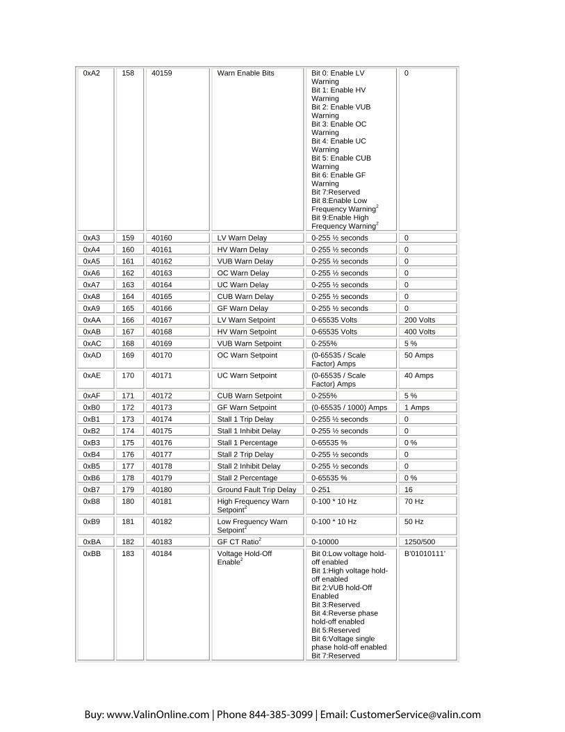
0xA2 158 40159 Warn Enable Bits Bit 0: Enable LV Warning Bit 1: Enable HV Warning Bit 2: Enable VUB Warning Bit 3: Enable OC Warning Bit 4: Enable UC Warning Bit 5: Enable CUB Warning Bit 6: Enable GF Warning Bit 7:Reserved Bit 8:Enable Low Frequency Warning2
Bit 9:Enable High Frequency Warning2
0
0xA3 159 40160 LV Warn Delay 0-255 ½ seconds 0 0xA4 160 40161 HV Warn Delay 0-255 ½ seconds 0 0xA5 161 40162 VUB Warn Delay 0-255 ½ seconds 0 0xA6 162 40163 OC Warn Delay 0-255 ½ seconds 0 0xA7 163 40164 UC Warn Delay 0-255 ½ seconds 0 0xA8 164 40165 CUB Warn Delay 0-255 ½ seconds 0 0xA9 165 40166 GF Warn Delay 0-255 ½ seconds 0 0xAA 166 40167 LV Warn Setpoint 0-65535 Volts 200 Volts 0xAB 167 40168 HV Warn Setpoint 0-65535 Volts 400 Volts 0xAC 168 40169 VUB Warn Setpoint 0-255% 5 % 0xAD 169 40170 OC Warn Setpoint (0-65535 / Scale
Factor) Amps 50 Amps
0xAE 170 40171 UC Warn Setpoint (0-65535 / Scale Factor) Amps
40 Amps
0xAF 171 40172 CUB Warn Setpoint 0-255% 5 % 0xB0 172 40173 GF Warn Setpoint (0-65535 / 1000) Amps 1 Amps 0xB1 173 40174 Stall 1 Trip Delay 0-255 ½ seconds 0 0xB2 174 40175 Stall 1 Inhibit Delay 0-255 ½ seconds 0 0xB3 175 40176 Stall 1 Percentage 0-65535 % 0 % 0xB4 176 40177 Stall 2 Trip Delay 0-255 ½ seconds 0 0xB5 177 40178 Stall 2 Inhibit Delay 0-255 ½ seconds 0 0xB6 178 40179 Stall 2 Percentage 0-65535 % 0 % 0xB7 179 40180 Ground Fault Trip Delay 0-251 16 0xB8 180 40181 High Frequency Warn
Setpoint2 0-100 * 10 Hz 70 Hz
0xB9 181 40182 Low Frequency Warn Setpoint2
0-100 * 10 Hz 50 Hz
0xBA 182 40183 GF CT Ratio2 0-10000 1250/500 0xBB 183 40184 Voltage Hold-Off
Enable2 Bit 0:Low voltage hold-off enabled Bit 1:High voltage hold-off enabled Bit 2:VUB hold-Off Enabled Bit 3:Reserved Bit 4:Reverse phase hold-off enabled Bit 5:Reserved Bit 6:Voltage single phase hold-off enabled Bit 7:Reserved
B’01010111’
Buy: www.ValinOnline.com | Phone 844-385-3099 | Email: [email protected]

Bit 8:Reserved Bit 9:Reserved Bit 10:Reserved Bit 11:Reserved Bit 12:Reserved Bit 13:Reserved Bit 14:Reserved Bit 15:Reserved
0x2153 8530 48531 MBAssembly500Wrd0 0-255 2 0x2154 8531 48532 MBAssembly500Wrd1 0-255 3 0x2155 8532 48533 MBAssembly500Wrd2 0-255 4 0x2156 8533 48534 MBAssembly500Wrd3 0-255 5 0x2157 8534 48535 MBAssembly500Wrd4 0-255 6 0x2158 8535 48536 MBAssembly500Wrd5 0-255 7 0x2159 8536 48537 MBAssembly500Wrd6 0-255 8 0x215A 8537 48538 MBAssembly500Wrd7 0-255 9 0x215B 8538 48539 MBAssembly500Wrd8 0-255 10 0x215C 8539 48540 MBAssembly500Wrd9 0-255 11 0x215D 8540 48541 MBAssembly500Wrd10 0-255 12 0x215E 8541 48542 MBAssembly500Wrd11 0-255 13 0x215F 8542 48543 MBAssembly500Wrd12 0-255 14 0x2160 8543 48544 MBAssembly500Wrd13 0-255 15 0x2161 8544 48545 MBAssembly500Wrd14 0-255 16 0x2162 8545 48546 MBAssembly500Wrd15 0-255 17 0x2163 8546 48547 MBAssembly500Wrd16 0-255 18 0x2164 8547 48548 MBAssembly500Wrd17 0-255 19 0x2165 8548 48549 MBAssembly500Wrd18 0-255 20 0x2166 8549 48550 MBAssembly500Wrd19 0-255 21 0x2167 8550 48551 MBAssembly500Wrd20 0-255 22 0x2168 8551 48552 MBAssembly500Wrd21 0-255 23 0x2169 8552 48553 MBAssembly500Wrd22 0-255 24 0x216A 8553 48554 MBAssembly500Wrd23 0-255 25 0x216B 8554 48555 MBAssembly500Wrd24 0-255 26 0x216C 8555 48556 MBAssembly500Wrd25 0-255 27 0x216D 8556 48557 MBAssembly500Wrd26 0-255 28 0x216E 8557 48558 MBAssembly500Wrd27 0-255 29 0x216F 8558 48559 MBAssembly500Wrd28 0-255 30 0x2170 8559 48560 MBAssembly500Wrd29 0-255 31 0x2171 8560 48561 MBAssembly500Wrd30 0-255 102 0x2172 8561 48562 MBAssembly500Wrd31 0-255 103 0x2173 8562 48563 MBAssembly500Wrd32 0-255 104 0x2174 8563 48564 MBAssembly500Wrd33 0-255 105 0x2175 8564 48565 MBAssembly500Wrd34 0-255 106 0x2176 8565 48566 MBAssembly500Wrd35 0-255 107 0x2177 8566 48567 MBAssembly500Wrd36 0-255 108 0x2178 8567 48568 MBAssembly501Wrd0 0-255 109 0x2179 8568 48569 MBAssembly501Wrd1 0-255 110 0x217A 8569 48570 MBAssembly501Wrd2 0-255 111 0x217B 8570 48571 MBAssembly501Wrd3 0-255 112 0x217C 8571 48572 MBAssembly501Wrd4 0-255 113 0x217D 8572 48573 MBAssembly501Wrd5 0-255 114 0x217E 8573 48574 MBAssembly501Wrd6 0-255 115
Buy: www.ValinOnline.com | Phone 844-385-3099 | Email: [email protected]

0x217F 8574 48575 MBAssembly501Wrd7 0-255 116 0x2180 8575 48576 MBAssembly501Wrd8 0-255 117 0x2181 8576 48577 MBAssembly501Wrd9 0-255 118 0x2182 8577 48578 MBAssembly501Wrd10 0-255 119 0x2183 8578 48579 MBAssembly501Wrd11 0-255 120 0x2184 8579 48580 MBAssembly501Wrd12 0-255 121 0x2185 8580 48581 MBAssembly501Wrd13 0-255 122 0x2186 8581 48582 MBAssembly501Wrd14 0-255 123 0x2187 8582 48583 MBAssembly501Wrd15 0-255 124 0x2188 8583 48584 MBAssembly501Wrd16 0-255 125 0x2189 8584 48585 MBAssembly501Wrd17 0-255 126 0x218A 8585 48586 MBAssembly501Wrd18 0-255 127 0x218B 8586 48587 MBAssembly501Wrd19 0-255 128 0x218C 8587 48588 MBAssembly501Wrd20 0-255 129 0x218D 8588 48589 MBAssembly501Wrd21 0-255 130 0x218E 8589 48590 MBAssembly501Wrd22 0-255 131 0x218F 8590 48591 MBAssembly501Wrd23 0-255 2 0x2190 8591 48592 MBAssembly501Wrd24 0-255 3 1. Only applies to 777-XXX-KW/HP-P 2. Only applies to P1 series 3. Read only bit 4. Reserved bits should be maintained as 0
Note: For more information about the 777-P/P1, see the programming guide and installation manual for the 777-P/P1. All installation manuals and programming guides are available online at
Buy: www.ValinOnline.com | Phone 844-385-3099 | Email: [email protected]