fig. 8-1 asm chart elements m. morris mano & charles r ... · pdf filelogic and computer...
TRANSCRIPT

© 2001 Prentice Hall, Inc.M. Morris Mano & Charles R. KimeLOGIC AND COMPUTER DESIGN FUNDAMENTALS, 2e, Updated.
8-1
IDLE
R 0RUN
(b) Example of state box
000NameBinarycode
Register operationor output
(a) State box (c) Decision box
0 1Condition
0 1START
IDLE
PC 0
(e) Example of decision and condition output box
R 0
From decision box
Register operationor output
(d) Conditional output box
�
�
�
Fig. 8-1 ASM Chart Elements

© 2001 Prentice Hall, Inc.M. Morris Mano & Charles R. KimeLOGIC AND COMPUTER DESIGN FUNDAMENTALS, 2e, Updated.
8-2
0 1START
IDLE
ASM BLOCK
AVAIL
Entry
Exit
Q0
MUL0 MUL1
Exit Exit
0 1
A 0�
Fig. 8-2 ASM Block
© 2001 Prentice Hall, Inc.M. Morris Mano & Charles R. KimeLOGIC AND COMPUTER DESIGN FUNDAMENTALS, 2e, Updated.
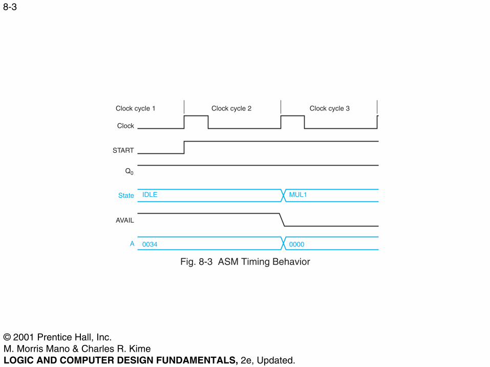
8-3
Clock cycle 1
Clock
START
Q0
State
AVAIL
A
IDLE MUL1
0034 0000
Clock cycle 2 Clock cycle 3
Fig. 8-3 ASM Timing Behavior

© 2001 Prentice Hall, Inc.M. Morris Mano & Charles R. KimeLOGIC AND COMPUTER DESIGN FUNDAMENTALS, 2e, Updated.
8-4
23 10111 Multiplicand
19 10011 Multiplier
10111
10111
00000
00000
437 110110101 Product
101110000
Fig. 8-4 Hand Multiplication Example

© 2001 Prentice Hall, Inc.M. Morris Mano & Charles R. KimeLOGIC AND COMPUTER DESIGN FUNDAMENTALS, 2e, Updated.
8-5
23 10111 Multiplicand
19 10011 Multiplier
00000 Initial partial product
10111 Add multiplicand, since multiplier bit is 1
10111 Partial product after add and before shift
010111 Partial product after shift
10111 Add multiplicand, since multiplier bit is 1
1000101 Partial product after add and before shifta
1000101 Partial product after shift
01000101 Partial product after shift
001000101 Partial product after shift
10111 Add multiplicand, since multiplier bit is 1
110110101 Partial product after add and before shift
437 0110110101 Product after final shift
a. Note that overflow temporarily occurred.
Fig. 8-5 Hardware Multiplication Example

© 2001 Prentice Hall, Inc.M. Morris Mano & Charles R. KimeLOGIC AND COMPUTER DESIGN FUNDAMENTALS, 2e, Updated.
8-6
Cout
n
n
n–1
Counter P
Zero detect
Controlunit
G (Go)
log2n
Qo
Z
Parallel adder
Multiplicand
Register B
Shift register A0 C Shift register Q
Multiplier
Product
OUT
IN
Control signals
n
n n
4
Fig. 8-6 Block Diagram for Binary Multiplier

© 2001 Prentice Hall, Inc.M. Morris Mano & Charles R. KimeLOGIC AND COMPUTER DESIGN FUNDAMENTALS, 2e, Updated.
8-7
0 1G
IDLE
Q0
MUL0
0 1Z
MUL1
C 0, A 0P n – 1
� �
�
A A + B,C Cout
�
�
C 0, C || A || Q sr C || A || Q,P P – 1
� �
�
0 1
Fig. 8-7 ASM Chart for Binary Multiplier

© 2001 Prentice Hall, Inc.M. Morris Mano & Charles R. KimeLOGIC AND COMPUTER DESIGN FUNDAMENTALS, 2e, Updated.
8-8
TABLE 8-1Control Signals for Binary Multiplier
Block DiagramModule Microoperation
Control Signal Name
ControlExpression
Register A: Initialize Load
Shift_dec
Register B: Load_B
Flip-Flop C: Clear_C Load —
Register Q: Load_QShift_dec —
Counter P: Initialize —Shift_dec —
A 0← IDLE G⋅A A B+← MUL0 Q0⋅C A Q sr C A Q← MUL1
B IN← LOADB
C 0← IDLE G⋅ MUL1+C Cout←
Q IN← LOADQC A Q sr C A Q←
P n 1–←P P 1–←
Table 8-1 Control Signals for Binary Multiplier
© 2001 Prentice Hall, Inc.M. Morris Mano & Charles R. KimeLOGIC AND COMPUTER DESIGN FUNDAMENTALS, 2e, Updated.
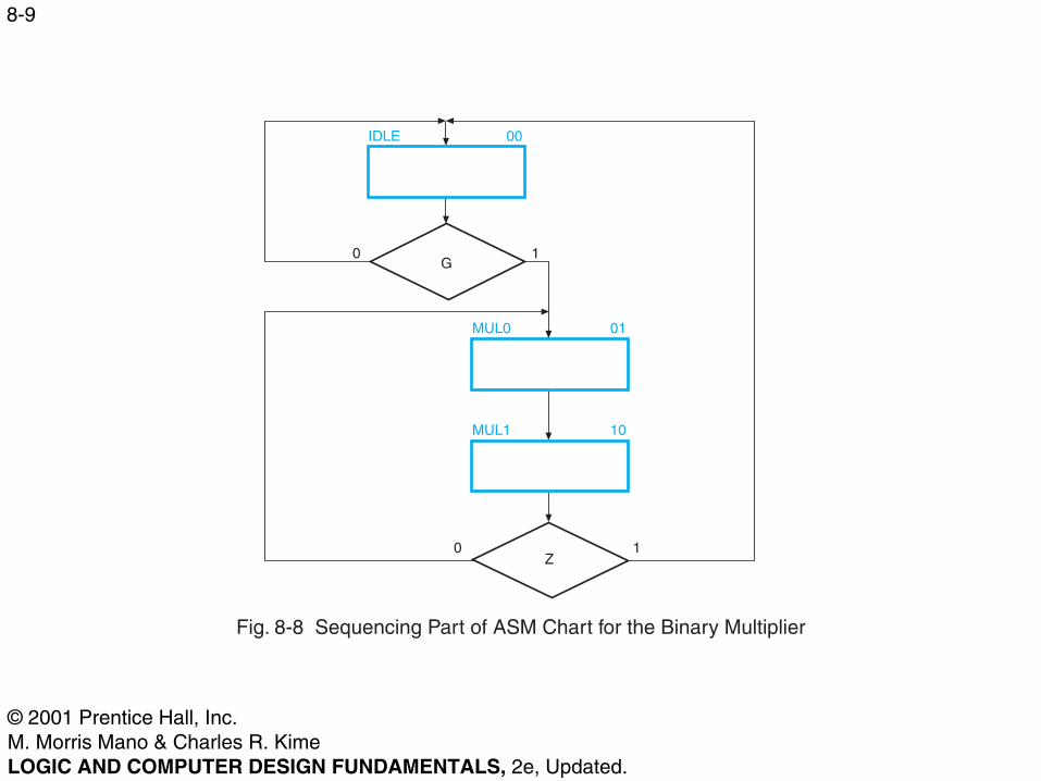
8-9
0 1G
IDLE
MUL0
0 1Z
01
MUL1 10
00
Fig. 8-8 Sequencing Part of ASM Chart for the Binary Multiplier

© 2001 Prentice Hall, Inc.M. Morris Mano & Charles R. KimeLOGIC AND COMPUTER DESIGN FUNDAMENTALS, 2e, Updated.
8-10
TABLE 8-2State Table for Sequence Register and Decoder Part of Multiplier Control Unit
Presentstate Inputs
Nextstate Decoder Outputs
Name M1 M0 G Z M1 M0 IDLE MUL0 MUL1
IDLE 0 0 0 � 0 0 1 0 00 0 1 � 0 1 1 0 0
MUL0 0 1 � � 1 0 0 1 0
MUL1 1 0 � 0 0 1 0 0 11 0 � 1 0 0 0 0 1
— 1 1 � � � � � � �
Table 8-2 State Table for Sequence Register and Decoder Part of Multiplier Control Unit

© 2001 Prentice Hall, Inc.M. Morris Mano & Charles R. KimeLOGIC AND COMPUTER DESIGN FUNDAMENTALS, 2e, Updated.
8-11
••IDLEMUL0MUL1
Initialize
Clear_C
Shift_dec
M0
Load
Clock
M1
G
Z
Q0
D
C
D
C
DECODERA0
A1
0
321
• •
••
•
•
•
Fig. 8-9 Control Unit for Binary Multiplier Using a Sequence Register and a Decoder

© 2001 Prentice Hall, Inc.M. Morris Mano & Charles R. KimeLOGIC AND COMPUTER DESIGN FUNDAMENTALS, 2e, Updated.
8-12
(a) State box
(b) Decision box
(c) Junction
(d) Conditional output box
0 1X
Entry
Exit 0Exit 1
Entry 1 Entry 2
Exit
Entry 1
Exit
Entry 2
• •
Entry
X
Exit 0 Exit 1
•Entry
X
Exit 1Control
Entry
Exit
State
EntryState
Exit
D
C
1X
Entry
Exit 1
Fig. 8-10 Transformation Rules for Control Unit with One Flip-Flop per State
•

© 2001 Prentice Hall, Inc.M. Morris Mano & Charles R. KimeLOGIC AND COMPUTER DESIGN FUNDAMENTALS, 2e, Updated.
8-13
••
D
C
IDLE
D
C
MUL0
D
C
MUL1
••
•
•
•
•
••
••
Initialize
Clear _C
Load
Shift_dec
Clock Z
Q0
3
1
G
2
4
34
1
1 4
2
•
Fig. 8-11 Control Unit with One Flip-Flop per State for the Binary Multiplier

© 2001 Prentice Hall, Inc.M. Morris Mano & Charles R. KimeLOGIC AND COMPUTER DESIGN FUNDAMENTALS, 2e, Updated.
8-14 -- Binary Multiplier with n = 4: VHDL Description-- See Figures 8-6 and 8-7 for block diagram and ASM Chartlibrary ieee;use ieee.std_logic_1164.all; use ieee.std_logic_unsigned.all;entity binary_multiplier is
port(CLK, RESET, G, LOADB, LOADQ: in std_logic;MULT_IN: in std_logic_vector(3 downto 0);MULT_OUT: out std_logic_vector(7 downto 0));
end binary_multiplier;
architecture behavior_4 of binary_multiplier istype state_type is (IDLE, MUL0, MUL1);signal state, next_state : state_type;signal A, B, Q: std_logic_vector(3 downto 0);signal P: std_logic_vector(1 downto 0);signal C, Z: std_logic;
beginZ <= P(1) NOR P(0); MULT_OUT <= A & Q;
state_register: process (CLK, RESET)begin
if (RESET = '1') thenstate <= IDLE;
elsif (CLK’event and CLK = '1') thenstate <= next_state;
end if;end process;
next_state_func: process (G, Z, state)begin
case state iswhen IDLE =>
if G = '1' thennext_state <= MUL0;
else next_state <= IDLE;
end if;when MUL0 =>
next_state <= MUL1;when MUL1 =>
if Z = '1' thennext_state <= IDLE;
else next_state <= MUL0;
end if;
Fig. 8-12 VHDL Description of a Binary Multiplier

© 2001 Prentice Hall, Inc.M. Morris Mano & Charles R. KimeLOGIC AND COMPUTER DESIGN FUNDAMENTALS, 2e, Updated.
8-15 end case;end process;
datapath_func: process (CLK)variable CA: std_logic_vector(4 downto 0);begin
if (CLK’event and CLK = '1') thenif LOADB = '1' then
B <= MULT_IN;end if;if LOADQ = '1' then
Q <= MULT_IN;end if;case state is
when IDLE => if G = '1' then
C <= '0';A <= "0000";P <= "11";
end if;when MUL0 =>
if Q(0) = '1' thenCA := ('0' & A) + ('0' & B);
else CA := C & A;
end if;C <= CA(4);A <= CA(3 downto 0);
when MUL1 =>C <= '0';A <= C & A(3 downto 1);Q <= A(0) & Q(3 downto 1);P <= P - "01";
end case;end if;
end process;end behavior_4;
Fig. 8-13 VHDL Description of a Binary Multiplier (Continued)
© 2001 Prentice Hall, Inc.M. Morris Mano & Charles R. KimeLOGIC AND COMPUTER DESIGN FUNDAMENTALS, 2e, Updated.
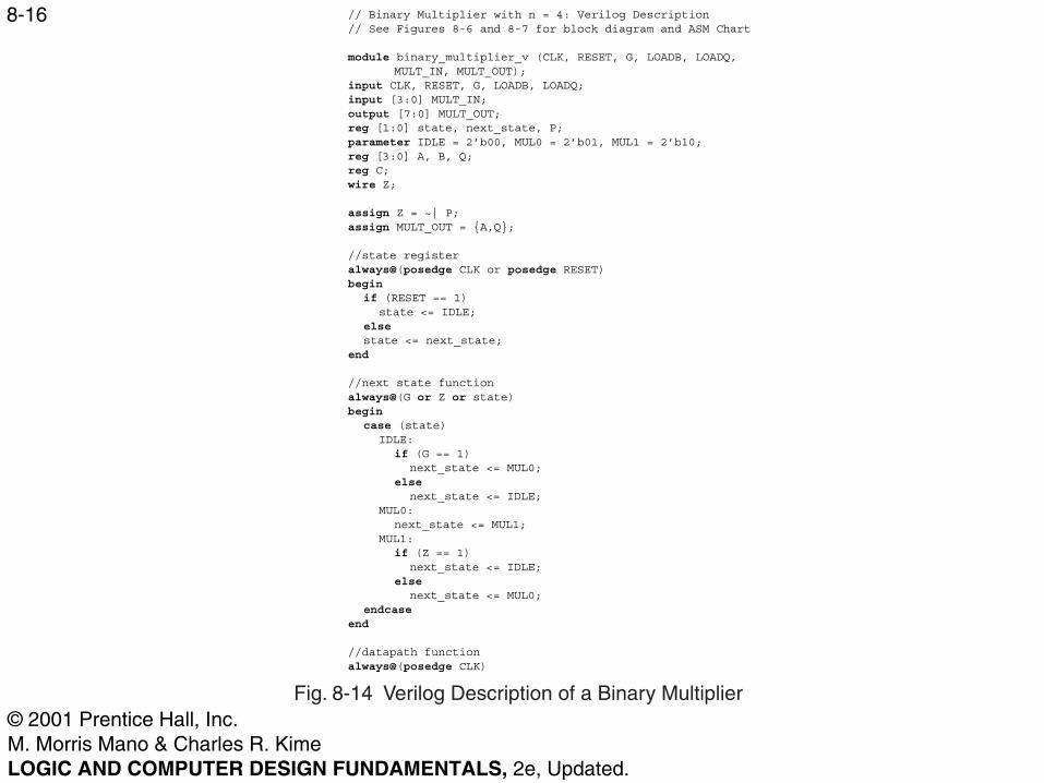
8-16 // Binary Multiplier with n = 4: Verilog Description// See Figures 8-6 and 8-7 for block diagram and ASM Chart
module binary_multiplier_v (CLK, RESET, G, LOADB, LOADQ,MULT_IN, MULT_OUT);
input CLK, RESET, G, LOADB, LOADQ;input [3:0] MULT_IN;output [7:0] MULT_OUT;reg [1:0] state, next_state, P;parameter IDLE = 2’b00, MUL0 = 2’b01, MUL1 = 2’b10;reg [3:0] A, B, Q;reg C;wire Z;
assign Z = ~| P;assign MULT_OUT = {A,Q};
//state registeralways@(posedge CLK or posedge RESET)begin
if (RESET == 1)state <= IDLE;
elsestate <= next_state;
end
//next state functionalways@(G or Z or state)begin
case (state)IDLE:
if (G == 1)next_state <= MUL0;
else next_state <= IDLE;
MUL0:next_state <= MUL1;
MUL1:if (Z == 1)
next_state <= IDLE;else
next_state <= MUL0;endcase
end
//datapath functionalways@(posedge CLK)
Fig. 8-14 Verilog Description of a Binary Multiplier
© 2001 Prentice Hall, Inc.M. Morris Mano & Charles R. KimeLOGIC AND COMPUTER DESIGN FUNDAMENTALS, 2e, Updated.
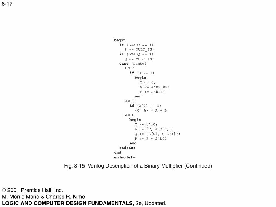
8-17
beginif (LOADB == 1)
B <= MULT_IN;if (LOADQ == 1)
Q <= MULT_IN;case (state)
IDLE:if (G == 1)
begin C <= 0;A <= 4’b0000;P <= 2’b11;
endMUL0:
if (Q[0] == 1){C, A} = A + B;
MUL1:begin
C <= 1’b0;A <= {C, A[3:1]};Q <= {A[0], Q[3:1]};P <= P - 2’b01;
endendcase
endendmodule
Fig. 8-15 Verilog Description of a Binary Multiplier (Continued)

© 2001 Prentice Hall, Inc.M. Morris Mano & Charles R. KimeLOGIC AND COMPUTER DESIGN FUNDAMENTALS, 2e, Updated.
8-18
Sequencer
Control address
Controlinputs Status signals from datapath
Next-addressgenerator
Control addressregister
Address
Controlmemory(ROM)
Data
Control data register(optional)
Next-addressinformation
Controloutputs
Control signalsto datapath
Microinstruction
Fig. 8-16 Microprogrammed Control Unit Organization

© 2001 Prentice Hall, Inc.M. Morris Mano & Charles R. KimeLOGIC AND COMPUTER DESIGN FUNDAMENTALS, 2e, Updated.
8-19
0 1G
IDLE
0 1Q0
MUL0
0 1Z
MUL1
000
INIT 001
010
ADD 011
A A + B,C Cout
�
�
C 0, C || A || Q sr C || A || Q,P P – 1
� �
�
A 0, C 0P n – 1
� �
�
100
Fig. 8-17 ASM Chart for Microprogrammed Binary Multiplier Control Unit

© 2001 Prentice Hall, Inc.M. Morris Mano & Charles R. KimeLOGIC AND COMPUTER DESIGN FUNDAMENTALS, 2e, Updated.
8-20
NXTADD1 NXTADD0 SEL DATAPATH
11 9 8 6 5 4 3 0
Fig. 8-18 Microinstruction Control Word Format

© 2001 Prentice Hall, Inc.M. Morris Mano & Charles R. KimeLOGIC AND COMPUTER DESIGN FUNDAMENTALS, 2e, Updated.
8-21
TABLE 8-3Control Signals for Microprogrammed Multiplier Control
Control Signal Register Transfers
States in WhichSignal is Active
Micro-instructionBit Position
SymbolicNotation
Initialize INIT 0 ITLoad ADD 1 LDClear_C INIT, MUL1 2 CCShift_dec MUL1 3 SD
A 0 P n 1–←,←A A B C Cout←,+←C 0←C A Q sr C A Q P P 1–←,←
Table 8-3 Control Signals for Microprogrammed Multiplier Control

© 2001 Prentice Hall, Inc.M. Morris Mano & Charles R. KimeLOGIC AND COMPUTER DESIGN FUNDAMENTALS, 2e, Updated.
8-22
TABLE 8-4SEL Field Definition for Binary Multiplier Control Sequencing
SEL
SequencingMicrooperations
Symbolicnotation
BinaryCode
NXT 00
DG 01
DQ 10
DZ 11
CAR NXTADD0←
G: CAR NXTADD0←G: CAR NXTADD1←
Q0: CAR NXTADD0←
Q0: CAR NXTADD1←
Z: CAR NXTA DD0←Z: CAR NXTADD1←
Table 8-4 SEL Field Definition for Binary Multiplier Control Sequencing
© 2001 Prentice Hall, Inc.M. Morris Mano & Charles R. KimeLOGIC AND COMPUTER DESIGN FUNDAMENTALS, 2e, Updated.
8-23
3
n
n
4Datapath
OUT
IN
2
5 x 12ControlMemory(ROM)
DATAPATH
SEL
NXTADD0
NXTADD1
CAR3
3
3
2
MUX1
2–to–1MUX
0
1
S
MUX2
4–to–1MUX
01
S1S0
23
0G
Q0Z
Fig. 8-19 Microprogrammed Control Unit for Multiplier
© 2001 Prentice Hall, Inc.M. Morris Mano & Charles R. KimeLOGIC AND COMPUTER DESIGN FUNDAMENTALS, 2e, Updated.
8-24
TABLE 8-5Register Transfer Description of Binary Multiplier Microprogram
Address Symbolic transfer statement
IDLEINITMUL0ADDMUL1
G: CAR INIT← G: CAR IDLE←,C 0← A 0← P n 1–← CAR MUL0←,, ,Q0: CAR ADD Q0: CAR MUL1←,←A A B C Cout CAR MUL1←,←,+←C 0 C A Q, sr C A Q , Z: CAR IDLE Z: CAR MUL0, ←,←← ←P P 1–←
Table 8-5 Register Transfer Description of Binary Multiplier Microprogram

© 2001 Prentice Hall, Inc.M. Morris Mano & Charles R. KimeLOGIC AND COMPUTER DESIGN FUNDAMENTALS, 2e, Updated.
8-25
TABLE 8-6Symbolic Microprogram and Binary Microprogram for Multiplier
Address NXTADD1 NXTADD0 SEL DATAPATH Address NXTADD1 NXTADD0 SEL DATAPATH
IDLE INIT IDLE DG None 000 001 000 01 0000INIT — MUL0 NXT IT, CC 001 000 010 00 0101MUL0 ADD MUL1 DQ None 010 011 100 10 0000ADD — MUL1 NXT LD 011 000 100 00 0010MUL1 IDLE MUL0 DZ CC, SD 100 000 010 11 1100
Table 8-6 Symbolic Microprogram and Binary Microprogram for Multiplier

© 2001 Prentice Hall, Inc.M. Morris Mano & Charles R. KimeLOGIC AND COMPUTER DESIGN FUNDAMENTALS, 2e, Updated.
8-26
(a) Register
OpcodeDestinationregister (DR)
Source reg-ister A (SA)
Source reg-ister B (SB)
15 9 8 6 5 3 2 0
(b) Immediate
OpcodeDestinationregister (DR)
Source reg-ister A (SA)
15 9 8 6 5 3 2 0
Operand (OP)
(c) Jump and Branch
OpcodeSource reg-ister A (SA)
15 9 8 6 5 3 2 0
Address (AD)Address (AD)(Left) (Right)
Fig. 8-20 Three Instruction Formats
© 2001 Prentice Hall, Inc.M. Morris Mano & Charles R. KimeLOGIC AND COMPUTER DESIGN FUNDAMENTALS, 2e, Updated.
8-27
Decimaladdress
Memorycontents
Decimalopcode
Other specifiedfields Operation
�R1 R2 � R3
�M [R4] R5
�R2 R7 + 3
25 0000101 001 010 011 5 (Subtract) DR:1, SA:2 SB:3
35 0100000 000 100 101 32 (Store) SA:4 SB:5
45 1000010 010 111 011 66 (Add Immedi-ate)
DR:2 SA:7 OP:3
70 0000000 011 000 000 Data = 192. After execution of instruction in 35, Data = 80.
�PC PC � 2055 1100011 101 110 100 96 (Branch on
zero)AD: 44 SA:6 If R6 = 0,
Fig. 8-21 Memory Representation of Instructions and Data

© 2001 Prentice Hall, Inc.M. Morris Mano & Charles R. KimeLOGIC AND COMPUTER DESIGN FUNDAMENTALS, 2e, Updated.
8-28
Instructionmemory215 x 16
Datamemory215 x 16
Register file8 x 16
Program counter(PC)
Fig. 8-22 Storage Resource Diagram for a Simple Computer

© 2001 Prentice Hall, Inc.M. Morris Mano & Charles R. KimeLOGIC AND COMPUTER DESIGN FUNDAMENTALS, 2e, Updated.
8-29
Bus ABus B
Address out
Data outMW
Data in
MUX B1 0
MUX D0 1
Address
Instructionmemory
Instruction
Zero fill
DA
BA
AA
FS
MD
RW
MW
CONTROL
DATAPATH
RW
DA
AA
Constantin
BA
Registerfile
D
A B
MB
FS
V
C
N
Z
Functionunit
A B
F
Data in Address
Datamemory
Data out
MDBus D
PC
MB
uction decoderInstr
JB
Extend
LP B
C
BranchControl
VCNZ
JBL
P BC
IR(8:6) || IR(2:0)
IR(2:0)
Fig. 8-23 Block Diagram for a Single-Cycle Computer
© 2001 Prentice Hall, Inc.M. Morris Mano & Charles R. KimeLOGIC AND COMPUTER DESIGN FUNDAMENTALS, 2e, Updated.
8-30
3 3 3
22 - 20 19 - 17 16 - 14 13 12 - 8 5 4
Instruction
Opcode DR SA SB
15 14 5 - 3 2 - 08 - 6
DA AA BA MB FS MD RW
3
MW
Control word
67
JB BC
2 - 0
1213 11 10 9
5
PL
••
•
•
•• •
•
•
•
••
•
•
• • •
Fig. 8-24 Diagram of Instruction Decoder

© 2001 Prentice Hall, Inc.M. Morris Mano & Charles R. KimeLOGIC AND COMPUTER DESIGN FUNDAMENTALS, 2e, Updated.
8-31
TABLE 8-7Truth Table for Instruction Decoder Logic
Instruction Function Type
Instruction Bits Control Word Bits
Bit 15 Bit 14 Bit 13 MB MD RW MW PL JB
ALU function using registers 0 0 0 0 0 1 0 0 XShifter function using registers 0 0 1 0 0 1 0 0 XMemory write using register data 0 1 0 0 X 0 1 0 XMemory read using register data 0 1 1 0 1 1 0 0 XALU operation using a constant 1 0 0 1 0 1 0 0 XShifter function using a constant 1 0 1 1 0 1 0 0 XConditional Branch 1 1 0 X X 0 0 1 0Unconditional Jump 1 1 1 X X 0 0 1 1
Table 8-7 Truth Table for Instruction Decoder Logic
© 2001 Prentice Hall, Inc.M. Morris Mano & Charles R. KimeLOGIC AND COMPUTER DESIGN FUNDAMENTALS, 2e, Updated.
8-32
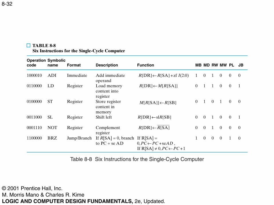
TABLE 8-8Six Instructions for the Single-Cycle Computer
Operationcode
Symbolicname Format Description Function MB MD RW MW PL JB
1000010 ADI Immediate Add immediate operand
1 0 1 0 0 0
0110000 LD Register Load memory content intoregister
0 1 1 0 0 1
0100000 ST Register Store register content inmemory
0 1 0 1 0 0
0011000 SL Register Shift left 0 0 1 0 0 1
0001110 NOT Register Complement register
0 0 1 0 0 0
01100000 BRZ Jump/Branch If R[SA] = 0, branch to PC + se AD
If R[SA] = 0, ,If R[SA] ≠ 0,
1 0 0 0 1
R DR[ ] R SA[ ] zf I(2:0)+←
R DR[ ] M R SA[ ][ ]←
M R SA[ ][ ] R SB[ ]←
R DR[ ] slR SB[ ]←
R DR[ ] R SA[ ]←
PC PC seAD+←PC PC 1+←
Table 8-8 Six Instructions for the Single-Cycle Computer

© 2001 Prentice Hall, Inc.M. Morris Mano & Charles R. KimeLOGIC AND COMPUTER DESIGN FUNDAMENTALS, 2e, Updated.
8-33
1 ns
4 ns
3 ns
1 ns
4 ns
1 ns
3 ns
PC
Instructionmemory
Register file(Read)
MUX B
MUX D
Functionunit orData memory
Register file(Write)
Fig. 8-25 Worst Case Delay Path in Single-Cycle Computer
© 2001 Prentice Hall, Inc.M. Morris Mano & Charles R. KimeLOGIC AND COMPUTER DESIGN FUNDAMENTALS, 2e, Updated.
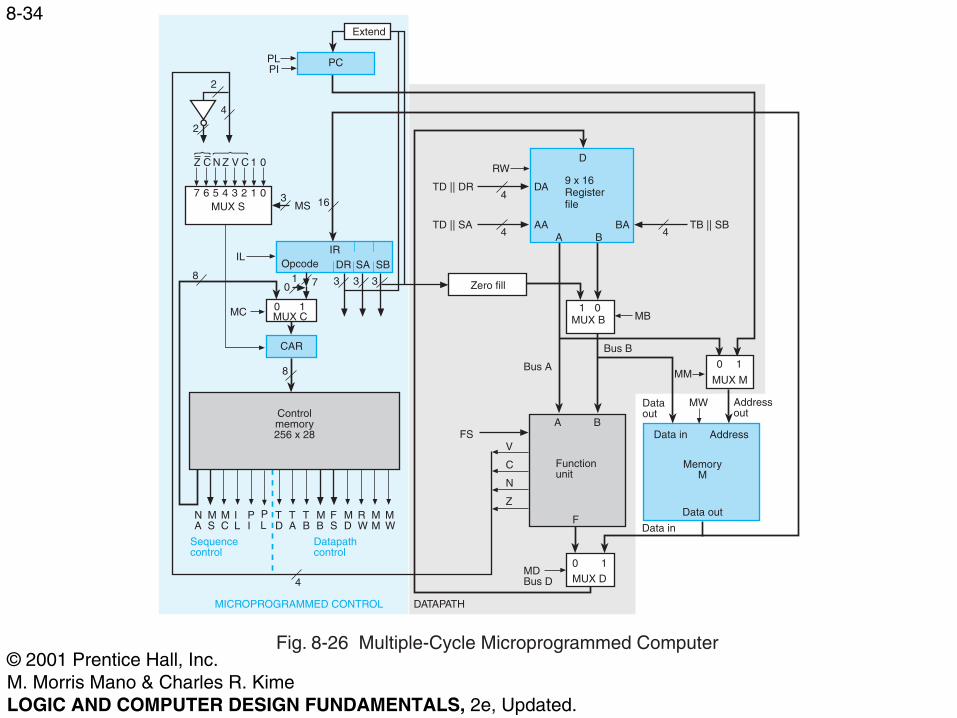
8-34
8
RW
4TD || DR
TD || SA4
PC
4
2
2
Z C N Z V C 1 0
7 6 5 4 3 2 1 0MUX S
3MS 16
ILIR
Opcode DR SA SB
3 3 3710
0 1MUX CMC
CAR
8
Controlmemory256 x 28
NA
MS
MC
IL
PI
TD
TA
TB
MB
FS
MD
RW
MM
MW
Sequencecontrol
Datapathcontrol
4
MICROPROGRAMMED CONTROL DATAPATH
PI
DA
AA
D
9 x 16Registerfile
A BBA
4TB || SB
MB1 0
MUX B
Bus B
Bus AMM
0 1
MUX M
Dataout
MW Addressout
Data in Address
MemoryM
Data out
Data in
A B
Functionunit
F
0 1
MUX DMDBus D
FSV
C
N
Z
Zero fill
PL
PL
Extend
••
Fig. 8-26 Multiple-Cycle Microprogrammed Computer
© 2001 Prentice Hall, Inc.M. Morris Mano & Charles R. KimeLOGIC AND COMPUTER DESIGN FUNDAMENTALS, 2e, Updated.
8-35
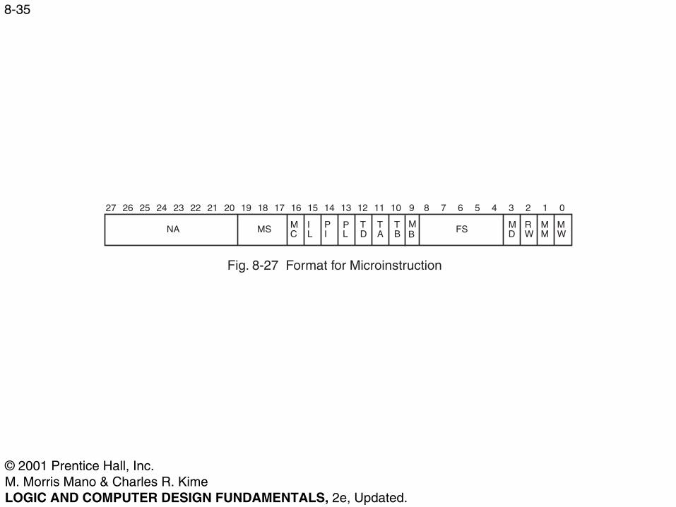
27 26 25 24 23 22 21 20 19 18 17 16 15 14 13 12 11 10 9 8 7 6 5 4 3 2 1 0
NA MS MC
IL
PI
TD
TA
TB FS M
DRW
MM
MW
MB
PL
Fig. 8-27 Format for Microinstruction

© 2001 Prentice Hall, Inc.M. Morris Mano & Charles R. KimeLOGIC AND COMPUTER DESIGN FUNDAMENTALS, 2e, Updated.
8-36
TABLE 8-9Control Word Information for Datapath
TD TA TB MB
Code
FS MD RW MM MW
CodeSelect Select Select Select Function Code Select Function Select Function
R[DR] R[SA] R[SB] Register 0 00000 FnUt No write (NW) Address No write (NW) 0
R8 R8 R8 Constant 1 00001 Data In Write (WR) PC Write (WR) 100010000110010000101001100011101000010100110001110100001010011000
F A=
F A 1+=F A B+=F A B 1+ +=F A B+=F A B 1+ +=F A 1–=F A=F A B∧=F A B∨=F A B⊕=F A=F B=F sr B=F sl B=
Table 8-9 Control Word Information for Datapath

© 2001 Prentice Hall, Inc.M. Morris Mano & Charles R. KimeLOGIC AND COMPUTER DESIGN FUNDAMENTALS, 2e, Updated.
8-37
TABLE 8-10Control Information for Sequence Control Fields
MS MC IL PI PL
CodeActionSymbolicNotation Code Select
SymbolicNotation Action
SymbolicNotation Action
SymbolicNotation Action
SymbolicNotation
Increment CAR CNT 000 NA NXA No load NLI No load NLP No load NLP 0Load CAR NXT 001 Opcode OPC Load instr. LDI Increment PC INP Load PC LDP 1If C � 1, load CAR; else increment CAR
BC 010
If V � 1, load CAR;else increment CAR
BV 011
If Z � 1, load CAR; else increment CAR
BZ 100
If N � 1, load CAR;else increment CAR
BN 101
If C � 0, load CAR;else increment CAR
BNC 110
If Z � 0, load CAR,else increment
CARBNZ 111
Table 8-10 Control Information for Sequence Control Fields
© 2001 Prentice Hall, Inc.M. Morris Mano & Charles R. KimeLOGIC AND COMPUTER DESIGN FUNDAMENTALS, 2e, Updated.
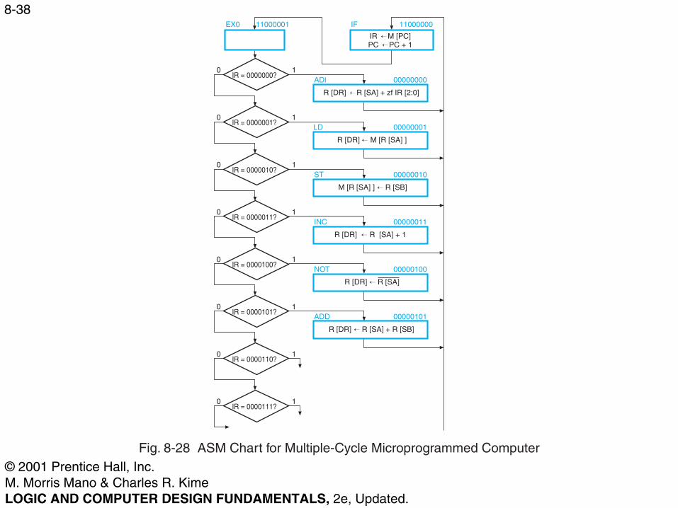
8-38
ST
INC
NOT
ADD
ADl
EX0 11000001
0 1IR = 0000000?
00000000
R [DR] R [SA] + zf IR [2:0]�
LD0 1
IR = 0000001?00000001
R [DR] M [R [SA] ]�
0 1IR = 0000010?
00000010
M [R [SA] ] R [SB]�
0 1IR = 0000011?
00000011
R [DR] R [SA] + 1�
0 1IR = 0000100?
00000100
R [DR] R [SA]�
0 1IR = 0000101?
00000101
R [DR] R [SA] + R [SB]�
0 1IR = 0000110?
0 1IR = 0000111?
IF 11000000
IR M [PC]�PC PC + 1�
Fig. 8-28 ASM Chart for Multiple-Cycle Microprogrammed Computer
© 2001 Prentice Hall, Inc.M. Morris Mano & Charles R. KimeLOGIC AND COMPUTER DESIGN FUNDAMENTALS, 2e, Updated.
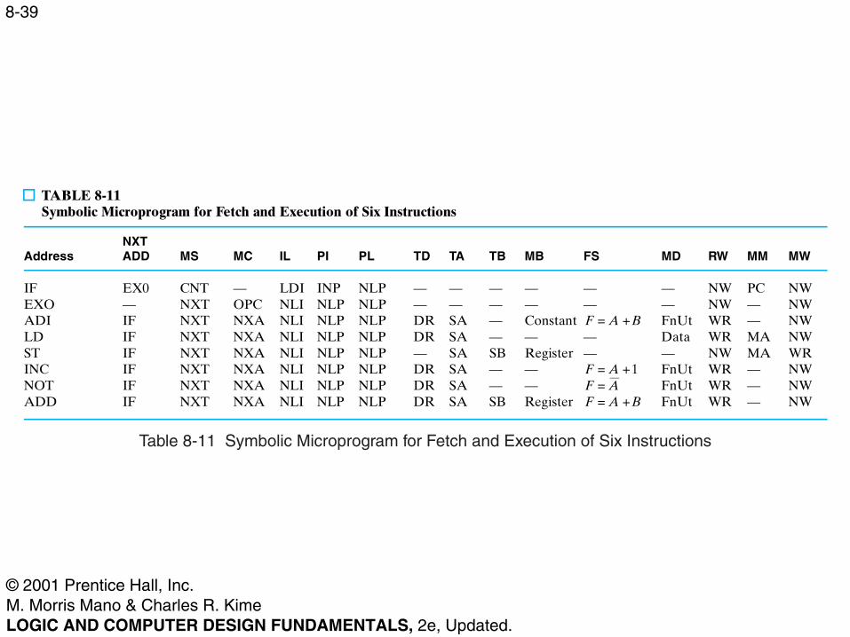
8-39
TABLE 8-11Symbolic Microprogram for Fetch and Execution of Six Instructions
AddressNXTADD MS MC IL PI PL TD TA TB MB FS MD RW MM MW
IF EX0 CNT — LDI INP NLP — — — — — — NW PC NWEXO — NXT OPC NLI NLP NLP — — — — — — NW — NWADI IF NXT NXA NLI NLP NLP DR SA — Constant FnUt WR — NWLD IF NXT NXA NLI NLP NLP DR SA — — — Data WR MA NWST IF NXT NXA NLI NLP NLP — SA SB Register — — NW MA WRINC IF NXT NXA NLI NLP NLP DR SA — — FnUt WR — NWNOT IF NXT NXA NLI NLP NLP DR SA — — FnUt WR — NWADD IF NXT NXA NLI NLP NLP DR SA SB Register FnUt WR — NW
F A B+=
F A 1+=F A=F A B+=
Table 8-11 Symbolic Microprogram for Fetch and Execution of Six Instructions
© 2001 Prentice Hall, Inc.M. Morris Mano & Charles R. KimeLOGIC AND COMPUTER DESIGN FUNDAMENTALS, 2e, Updated.
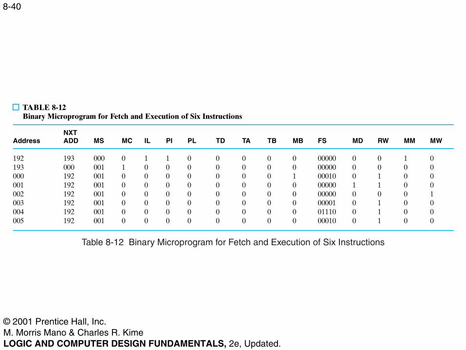
8-40
TABLE 8-12Binary Microprogram for Fetch and Execution of Six Instructions
AddressNXTADD MS MC IL PI PL TD TA TB MB FS MD RW MM MW
192 193 000 0 1 1 0 0 0 0 0 00000 0 0 1 0193 000 001 1 0 0 0 0 0 0 0 00000 0 0 0 0000 192 001 0 0 0 0 0 0 0 1 00010 0 1 0 0001 192 001 0 0 0 0 0 0 0 0 00000 1 1 0 0002 192 001 0 0 0 0 0 0 0 0 00000 0 0 0 1003 192 001 0 0 0 0 0 0 0 0 00001 0 1 0 0004 192 001 0 0 0 0 0 0 0 0 01110 0 1 0 0005 192 001 0 0 0 0 0 0 0 0 00010 0 1 0 0
Table 8-12 Binary Microprogram for Fetch and Execution of Six Instructions

© 2001 Prentice Hall, Inc.M. Morris Mano & Charles R. KimeLOGIC AND COMPUTER DESIGN FUNDAMENTALS, 2e, Updated.
8-41
LRI0
0 1IR = 0000110?
00000110
R8 M [R [ SA] ]�
LRI1 10000110
R [DR] M [R8]�
To IF
…
…
Fig. 8-29 ASM Chart for Register Indirect Instruction

© 2001 Prentice Hall, Inc.M. Morris Mano & Charles R. KimeLOGIC AND COMPUTER DESIGN FUNDAMENTALS, 2e, Updated.
8-42
0
SRM1
0 1IR = 0000111?
00000111
R8 zf IR [2:0]�
SRM2 10000111
R [DR] sr R [SA],�
…
…
1zf IR [2:0] = 0?
R8 R8 – 1�
R8 = 0?1
T0 IF
0
SRM3 10001000
T0 IF
NOTE: SA = DR
Fig. 8-30 ASM Chart for Right-Shift Multiple Instruction

© 2001 Prentice Hall, Inc.M. Morris Mano & Charles R. KimeLOGIC AND COMPUTER DESIGN FUNDAMENTALS, 2e, Updated.
8-43
Fig. 8-31 ASM Chart for Multiple-Cycle, Decoder-Based Computer
(ST)
(INC)
(NOT)
(ADD)
(ADl)
EX0 01
0 1IR = 0000000?
(LD)0 1IR = 0000001?
R [DR] M [R [SA] ]�
0 1IR = 0000010?
M [R [SA] ] R [SB]�
0 1IR = 0000011?
R [DR] R [SA] + 1�
0 1IR = 0000100?
R [DR] R [SA]�
0 1IR = 0000101?
R [DR] R [SA] + R [SB]�
0 1IR = 0000110?
IF 00
IR M [PC],�PC PC + 1�
(LRI)
R8 M [R [SA] ]�
R [DR] M [R8]�
R [DR] R [SA] + zf IR [2:0]�
EX1 10

© 2001 Prentice Hall, Inc.M. Morris Mano & Charles R. KimeLOGIC AND COMPUTER DESIGN FUNDAMENTALS, 2e, Updated.
8-44
Fig. 8-32 Block Diagram of Hardwired Counter and Decoder-Based, Multiple-Cycle Control Unit
CR
Decoder
Control logicDecoder
ADILDSTINCNOTADDLRI
0123456
CR
IL
PI
TD
TA
TB
MB
FS
MD
RW
MM
MW
IR
91011
IL
Syn. resetCounter
0 1 2IF
EX
EX
0 1

© 2001 Prentice Hall, Inc.M. Morris Mano & Charles R. KimeLOGIC AND COMPUTER DESIGN FUNDAMENTALS, 2e, Updated.
8-45
WAREHOUSE
Fig. 8-33 Assembly Line Analogy to Computer Pipeline
© 2001 Prentice Hall, Inc.M. Morris Mano & Charles R. KimeLOGIC AND COMPUTER DESIGN FUNDAMENTALS, 2e, Updated.
8-46
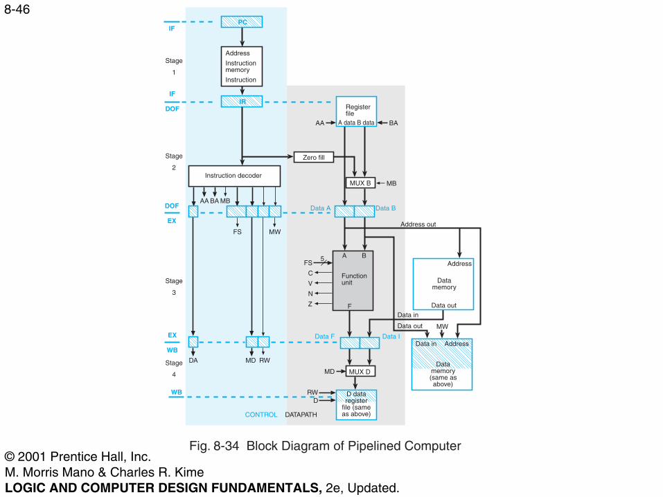
Fig. 8-34 Block Diagram of Pipelined Computer
IF
IF
DOF
Stage
1
Address
Instructionmemory
Instruction
DOF
EX
EX
WB
Stage
2
Stage
3
AA BA
Registerfile
A data B data
Zero fill
Instruction decoderMUX B MB
Data A Data B
Address outFS MW
AA BA MB
FS
C
V
N
Z
A B
Functionunit
MDDA RWStage
4
WB
F
MD MUX D
RWD
D dataregister
file (sameas above)
Datamemory(same asabove)
Data F Data IData in Address
Data in
Data out MW
Data out
Datamemory
Address
CONTROL DATAPATH
5
PC
IR
© 2001 Prentice Hall, Inc.M. Morris Mano & Charles R. KimeLOGIC AND COMPUTER DESIGN FUNDAMENTALS, 2e, Updated.
8-47
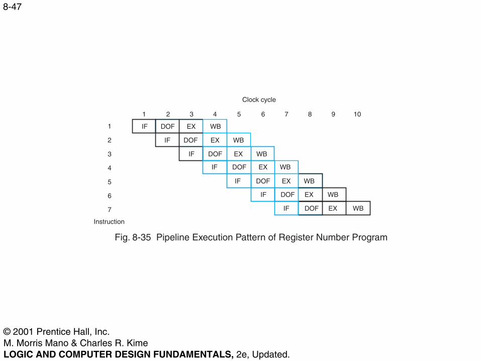
1
2
3
4
5
6
7
Instruction
1 2 3 4 5 6 7 8 9 10
Clock cycle
DOF EX WB
DOF EX WB
DOF EX WB
DOF EX WB
DOF EX WB
DOF EX WB
DOF EX WB
IF
IF
IF
IF
IF
IF
IF
Fig. 8-35 Pipeline Execution Pattern of Register Number Program
© 2001 Prentice Hall, Inc.M. Morris Mano & Charles R. KimeLOGIC AND COMPUTER DESIGN FUNDAMENTALS, 2e, Updated.
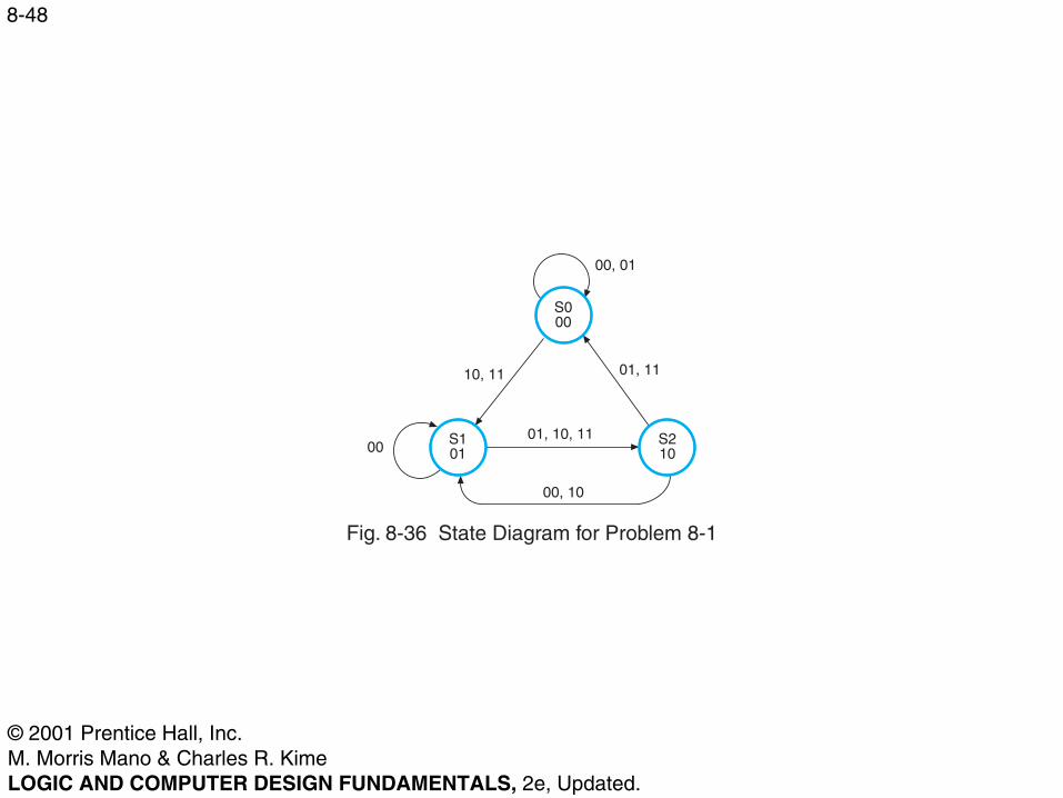
8-48
S000
S101
S210
10, 11 01, 11
00, 01
01, 10, 11
00, 10
00
Fig. 8-36 State Diagram for Problem 8-1