fig. 1. schematic of the thermal-structural finite element
TRANSCRIPT
FINITE ELEMENT ANALYSIS OF FABRICATION RELATED THERMAL EFFECTS IN
CAPACITIVE MICROMACHINED ULTRASONIC TRANSDUCERS
Mario Kupnik∗, Arif S. Ergun∗, Goksen G. Yaralioglu∗, Baris Bayram,Omer Oralkan∗, Serena H. Wong∗, Dersong Lin∗, and Butrus T. Khuri-Yakub∗
∗Edward L. Ginzton Laboratory, Stanford University, Stanford, CA-94305-4088
Abstract – The accurate prediction of the staticoperation point of capacitive micromachined ultrasonictransducer (CMUT) membranes is essential for dy-namic performance modeling, device design, and devicefabrication. We evaluate whether fabrication-relatedstress effects in CMUT cells cause significant deviationsobserved between membrane deflection measurementsand calculations. Our finite element analysis (FEA)considers the thermal structural interaction associatedwith the temperature stress history during device fab-rication. Specific boundary conditions enable thermalexpansion in all directions. Compared to conventionalFEAs with one static solution step, we use seven staticsolution steps using the element birth and death featureof ANSYS to assemble the CMUT cell layer by layerat the appropriate deposition temperatures. We usemeasured static deflection profiles of metallized andnon-metallized membranes with different diameters andthicknesses to extract all unknown parameters forthe model. This approach improves the prediction ofmembrane deflections significantly, and it explains whypresent models often overestimate the collapse voltage.
I. INTRODUCTION
In a vacuum sealed CMUT cell, the ambient pres-sure and the DC bias voltage, which is applied duringdevice operation, contribute to the static membranedeflection. When the sacrificial release method [1]is used to fabricate the device, the inherent residualstress [2]–[4] of the deposited film (low-stress siliconnitride layer) also influences the membrane deflection.
The accurate prediction of the static membranedeflection is essential for all subsequent dynamicperformance modeling steps in FEA. That is to saythat only if the model is capable to determine the staticoperation point of the CMUT membrane correctly,the modal, harmonic, or transient simulation runs, allprestressed, will give results, worth to be compareddirectly to measurement results. This especially ap-plies to the accurate prediction of the collapse voltage,which is an important criterion for the design andoperation of a CMUT.
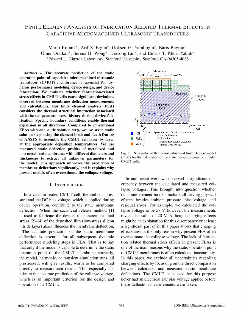
Fig. 1. Schematic of the thermal-structural finite element model(FEM) for the calculation of the static operation point of circularCMUT cells.
In our recent work we observed a significant dis-crepancy between the calculated and measured col-lapse voltages. This brought into question whetherour finite element models include all driving physicaleffects, besides ambient pressure, bias voltage, andresidual stress. For example, we calculated the col-lapse voltage to be 58 V, however, the measurementsrevealed a value of 20 V. Although charging effectsmight be an explanation for this discrepancy or at leasta significant part of it, this paper shows that chargingeffects are not the only reason why present FEA oftenoverestimate the collapse voltage. The lack of fabrica-tion related thermal stress effects in present FEAs isone of the main reasons why the static operation pointof CMUT membranes is often calculated inaccurately.In this paper, we exclude all uncertainties regardingcharging effects by focussing on the direct comparisonbetween calculated and measured static membranedeflections. The CMUT cells used for this purposenever had an electrical DC bias voltage applied beforethese deflection measurements were taken.
938©1051-0117/06/$20.00 2006 IEEE 2006 IEEE Ultrasonics Symposium

Fig. 2. Illustration of how the element birth and death feature of ANSYS is used to assemble the CMUT cell layer by layer in sevensteps in the solution part of the FEA. The parts of the structure, which are illustrated in a transparent fashion in this figure, only consistof elements, which are all killed during the specific solution step.
II. THERMAL-STRUCTURAL FEA FOR CMUTS
In addition to the commonly used electrical-structural domain, our FEA is characterized by anextension into a thermal domain with its main con-sequence of thermal expansion. Therefore, the FEAis able to consider fabrication related thermal stresseffects in CMUTs.
Our FEM (Fig. 1) represents the most used structurefor CMUT cells, when fabricated with the sacrificialrelease method [1]. Because the test devices fabricatedfor verification purpose only had circular cells, anaxisymmetric 2D model can be used as good approxi-mation. However, the same thermal-structural domainextension can be applied easily to more sophisticated3D models for all other cell shapes. Compared to otherFEAs, our model is distinguished by the followingfour features: First, the whole substrate (500 µm ofsilicon) below the membrane is modeled; Second, allrelated material properties (Fig. 1) are put into themodel as a function of temperature. These propertiesneed to be specified over a large temperature range,i.e. up to the maximum temperature that occurs duringthe device fabrication; Third, the model has veryspecific boundary conditions, that enable the wholestructure to expand or contract in both x and ydirection when a thermal load is applied (Fig. 1).The nodes on the bottom side of the substrate areonly constrained in x-direction to allow the model toexpand or contract in y-direction. The nodes at the
right side of the model are all coupled to move onlythe same amount in x-direction by using a masterdegree of freedom [6]. Coupling these nodes mimicsan infinite extension of material around the circularcell, which is required because of the transition fromthe silicon to the silicon nitride layer; Fourth, insteadof only one solution step in the solution part of theFEA, seven steps that mimic the fabrication process(7-step model), are used. This last feature is describedin more detail in the rest of this section:
In the seven solution steps of the 7-step model,the element birth and death feature (ekill, ealive [6])of ANSYS is utilized to assemble the CMUT celllayer by layer at the related deposition temperatures(Fig. 2). Killing an element before a solution stepmeans that the stiffness matrix of that element ismultiplied by a small multiplication factor (10−6
by default), which deactivates the element for thissolution step. The order of the steps reflects thesituation according to the two main events during thedevice fabrication concerning thermal stress effects.These two main events are a silicon nitride depositionand a metal (aluminum) deposition step. The siliconnitride layer is built by all together three depositionsat 780 ◦C in a low-stress LPCVD step with twointervening fabrication steps to define the gap, i.e. apoly silicon deposition (sacrificial layer) and a potas-sium hydroxide (KOH) step (releasing the membrane).These five fabrication steps are approximated in the
939 2006 IEEE Ultrasonics Symposium

model by assuming that the silicon nitride membraneis completely formed in one single fabrication step,which is modeled by solution steps 1, 2 and 3 (Fig. 2).The metal deposition step to build the electrode isdone at a specific deposition temperature TDep, whichrequires the solution steps 4, 5, and 6 (Fig. 2).The ambient pressure, the DC bias voltage, and theoperating temperature of the CMUT are applied inthe seventh and final solution step, which reveals thestatic operation point of the CMUT cell, i.e. the staticmembrane deflection.
III. MODEL PARAMETER EXTRACTION
Before the FEA can be verified by a comparisonof calculated and measured membrane deflections,all related material properties and fabrication relateddeposition temperatures need to be determined. TheYoung’s modulus and the Poisson ratio of the lowstress silicon nitride, which we deposited in a LPCVDtube at the Stanford Nanofabrication Facility (SNF),are known from previous work [5]. In this context,the unknown parameters are the coefficient of thermalexpansion (CTEX) and the intrinsic stress of the lowstress silicon nitride, as well as the temperature of themembrane during the metal deposition step, i.e. TDep
(Fig 2).The basic idea of how to extract these three parame-
ters is to measure both the static membrane deflectionsbefore and after the metal deposition step. Thus, theproblem to determine all three unknown parameterscan be split up in two simpler tasks (Fig. 3, opti-mization 1 and optimization 2): First, the parametersfor the intrinsic stress and the coefficient of thermalexpansion of the silicon nitride were adapted in anoptimization run for best average fit to the membranedeflection measurement results obtained before themetal deposition step; Second, the temperature of themembrane during the metal deposition (TDep) wasadapted for best average fit to the measurements,obtained after the metal deposition step. For bothoptimization runs, we used 12 representative cellgeometries on the wafers fabricated, i.e. cell diametersof 24, 30, and 36 µm and membrane thicknessesfrom 400 to 900 nm. The deposition thickness ofthe aluminum (half-metallization) ranged from 100 to300 nm. A white light 3D surface profiler (New View100, Zygo Corporation, Middlefield, CT) was used tomeasure the static membrane deflection profiles underthe atmospheric pressure of 1 atm.
Fig. 3. Illustration of how all unknown model parameters areextracted in two subsequent optimization runs, using two sets ofmembrane deflection measurement data, obtained before and afterthe metallization step.
IV. RESULTS AND VERIFICATION
The result of the first optimization run (Fig. 3)shows that the low stress silicon nitride has a 7.9%larger CTEX value than of silicon and that the intrinsicstress in the membrane is 84 MPa tensile. As expected,using these two parameters in the FEA improves theprediction of the membrane center deflection beforethe metal deposition step significantly from -31.8%(σ = 16%) to 0.4% (σ = 10.3%), as depicted in Fig. 4.
The second optimization run (Fig. 3) determinesan average metal deposition temperature (TDep) of62.3 ◦C (σ = 21.4 ◦C), which gives the best averagefit (orange curve, Fig. 5) to the measurement resultsfor various cell geometries, i.e. three different groupsof cell diameters (24, 30, and 36 µm).
However, for small center deflections, i.e. cells witha diameter of 24 µm, the model overestimates thestatic center deflections. For large center deflections(36 µm cells) the model underestimates the deflec-tions. The reason for these deviations seems to bethat CMUT cells with larger diameters heat up moreduring the metal deposition step, especially in thecenter region of the membrane. Note that the cellsare vacuum sealed and the main heat flow betweenmembrane and substrate happens at the post regionof the cell. If the optimization run (Fig. 3) is donefor three separate groups, i.e. for 24, 30, and 36 µmdiameters, this assumption is supported and the FEAcan be further improved. The optimum value for TDep
is 82.6 ◦C (σ = 21.6 ◦C), 61.0 ◦C (σ = 9.18 ◦C), and43.1 ◦C (σ = 9.31 ◦C) for 36 µm, 30 µm, and 24 µmcell diameters, respectively.
It is clear from Fig. 5 that after the metalliza-
940 2006 IEEE Ultrasonics Symposium

5 10 15 20 25 30
-60-50-40-30-20-10
0102030
Rel
ativ
e de
viat
ion
(%)
befo
re m
etal
lizat
ion
1-step modelno residual stress
avrg = - 31.8 % (σ = 16 %)
Center deflection (nm)
avrg = 0.4 % (σ = 10.3 %) 7-step model84 MPa tensile intrinsic
7.9 % ∆CTEX to Si
Fig. 4. Relative deviations between measured and calculatedstatic membrane center deflections, for different cell geometries,before the metal deposition step. Each data point corresponds toa certain cell geometry.
tion step, the thermal stress between the aluminumelectrode and the silicon nitride membrane is themain reason why present FEAs underestimate thestatic membrane deflections (green curve, Fig. 5), and,therefore, overestimate the collapse voltage. This iseven valid when these models consider the residualstress in the silicon nitride membrane (blue curve,Fig. 5). Further, it is worth to mention that thesecells never had an electrical DC bias voltage appliedbefore these profile measurements, which shows thatcharging effects are not required as explanation to whypresent models often underestimate the membranedeflection and therefore overestimate the collapsevoltage.
V. CONCLUSION
This paper demonstrates that present FEAs donot consider all physical effects that have significantinfluence on the static membrane deflection. Thelack of fabrication related thermal stress effects inpresent FEAs is one of the main reasons why thestatic operation point (static membrane deflection) ofCMUT cells is often calculated inaccurately. Further,our results explain why present FEAs overestimatethe collapse voltage. The main part of the improve-ment concerning the prediction of the static centerdeflection (88%) comes from the fact that the modelconsiders the thermal expansion coefficient mismatchbetween the aluminum electrode and the nitride mem-brane. For “thermal-stress-sensitive” CMUT designs(large cell diameters, thin membranes, small gaps,thick electrodes, not full metallized), metals other
0 20 40 60 80 100 120 140 160
-80-70-60-50-40-30-20-10
010203040
TDep = TOp= 20°C
Exponential functionavrg = - 41.3 % (σ = 14.7 %)
avrg = - 47.7 % (σ = 12.5 %)
avrg = + 6.9 % (σ = 20.2 %)
7 - step model, 84 MPa tensile intrinsic, 7.9 % ∆CTEX to Si, TDep= 62.3°C
7 - step model, 84 MPa tensile intrinsic, 7.9 % ∆CTEX to Si,
1 - step model, no residual stress
Rel
ativ
e de
viat
ion
(%)
afte
r met
alliz
atio
n
Center deflection (nm)
Fig. 5. Relative deviations between measured and calculatedstatic membrane center deflections, for different cell geometries,after the metal deposition step (aluminum, half-metallization).Three models with different parameter sets are compared
than aluminum as CMUT electrode material should beconsidered, e.g. a titanium base layer with a platinumelectrode. Further, our model predicts that full met-allized cells are less sensitive to stress effects relatedto the thermal mismatch between the electrode andmembrane and it is suitable for investigations of theCMUT behavior at different operation temperatures.
ACKNOWLEDGMENT
Mario Kupnik acknowledges the FWF AustrianScience Fund for financial support.
REFERENCES
[1] A. S. Ergun, Y. Huang, X. Zhuang, O. Oralkan, G. .G. Yarali-oglu, and B. T. Khuri-Yakub, “Capacitance Microma-chined Ultrasonic Transducers: Fabrication Technology,”IEEE Trans. Ultrason., Ferroelect., Freq. Contr., vol. 52, pp.2242–2258, 2005.
[2] A. Tarraf, J. Daleiden, S. Irmer, D. Prasai, and H. Hilmer,“Stress investigation of PECVD dielectric layers for advancedoptical MEMs,” J. Micromech. Microengineering, vol. 14, pp.317–323, 2004.
[3] Y. Toivola, J. Thurn, R. Cook, G. Cibuzar, and K. Roberts,“Influence of deposition conditions on mechanical propertiesof low-pressure chemical vapor deposited low-stress siliconnitride films,” J. Applied Physics, vol. 94, pp. 6915–6922,2003.
[4] P. Temple-Boyer, C. Rossi, E. Saint-Etienne, and E. Scheid,“Residual stress in low pressure chemical vapor depositionSiNx films deposited from silane and ammonia,” J. Vac. Sci.Technol. A, vol. 16, pp. 2003–2007, 1998.
[5] G. .G. Yaralioglu, A. S. Ergun, B. Bayram, T. Marentis, andB. T. Khuri-Yakub, “Residual Stress and Young’s ModulusMeasurement of Capacitive Micromachined Ultrasonic Trans-ducer Membranes,” in Proc. IEEE Ultrason. Symp., 2001,pp. 953–956.
[6] ANSYS 10.0 Manual, Ansys Inc., Canonsburg, PA.
941 2006 IEEE Ultrasonics Symposium