field emission from carbon nanotubes - university...
TRANSCRIPT

Field emission from carbon nanotubes
Author: Mojca Rangus Mentor: Professor Dragan Mihailovic
23.4.2003
Abstract
Carbon nanotubes, a new form of carbon discovered in 1991, have been rapidly rec-ognized as one of the most promising electron field emitters ever since the first emissionexperiments reported in 1995. Their potential as emitters in various devices has beenamply demonstrated during the last eight years, and recent developments of productiontechniques are likely to trigger future applications.
Contents
1 Introduction 2
2 Field emission 32.1 Total energy distribution . . . . . . . . . . . . . . . . . . . . . . . . . . . . . 32.2 Transmission function . . . . . . . . . . . . . . . . . . . . . . . . . . . . . . 42.3 Fowler-Nordheim equation . . . . . . . . . . . . . . . . . . . . . . . . . . . . 52.4 Electric field at sharp points . . . . . . . . . . . . . . . . . . . . . . . . . . . 6
3 Field emission from carbon nanotubes 73.1 Carbon nanotubes . . . . . . . . . . . . . . . . . . . . . . . . . . . . . . . . 73.2 Field emission from carbon nanotubes . . . . . . . . . . . . . . . . . . . . . 7
3.2.1 Field emission energy distribution and workfunction . . . . . . . . . 93.2.2 Single carbon nanotubes and carbon films . . . . . . . . . . . . . . . 123.2.3 Emitter degradation . . . . . . . . . . . . . . . . . . . . . . . . . . . 15
4 Applications 15
5 Conclusion 18
1

1 Introduction
Field emission involves the extraction of electrons from a solid by tunneling through thesurface potential barrier. The emitted current depends directly on the local electric fieldat the emitting surface E and on its work function φe. In fact, a simple model (the Fowler-Nordheim model) shows that the dependence of the emitted current on the local electricfield and the work function is exponential-like. As a consequence, a small variation of theshape or surrounding of the emitter (geometric field enhancement) and/or the chemicalstate of the surface has a strong impact on the emitted current. For those reasons theideal emitter should be very long and very thin, made of conductive material with highmechanical strength, be robust, and along all that cheap and easy to process [1].
Since its theoretical formulation thermionic emission (TE) has been a key concept inelectron-beam techniques. In thermionic electron emission, the solid electron source (thecathode) is heated above 2000◦C to allow free electrons to escape from the surface. Thegreatest advantage of this so called ”hot cathode” is that it works even in low-vacuum (non-UHV) ambiences, which contain vast numbers of gaseous molecules. However, hot cathodestend to get thinner and thinner over a long period of time due to chemical reactions withresidual water, oxidation and sublimation of oxides. In addition, hot cathodes requirea power supply for heating, and therefore is difficult to construct a compact thermionicemission device [2].
In the mid-1950s it was suggested that these disadvantages of hot cathodes may beovercome by replacing them with field emission (FE), or so called ¨cold”, cathodes. Whena high electric field in the order of 107 V/cm is applied on a solid surface with a negativeelectrical potential, electrons inside the solid are emitted into vacuum by the quantummechanical tunneling effect. This phenomenon is called field emission of electrons. Thiskind of emission of electrons was one of the earliest conformations of tunneling as predictedin the new quantum theory of the 1920s.
Historically, the first observed field emissions have probably occurred in many earlyhigh-voltage experiments in evacuated containers, but first detailed description was givenby Wood in 1897. Field emission did not progress much either experimentally or theoret-ically until the late 1920s. It was only with the development of quantum mechanics andthe Sommerfeld electron theory of metals, that the field emission theory was developed byFowler and Nordheim. The dependence of emission current density J on the metal workfunction φe and strong electric field F is known as Fowler-Nordheim (F-N) equation [3].
In 1950s some new approaches to improve the transmission function were taken andtherefore some new approximations of energy distribution were developed.
Field emission and tunneling through vacuun is also used by scanning tunneling micro-scope (STM). STM is widely used in both industrial and fundamental research to obtainatomic-scale images of metal surfaces. It provides a three-dimensional profile of the surfacewhich is very useful for characterizing surface roughness, observing surface defects, anddetermining the size and conformation of molecules and aggregates on the surface. Theelectron cloud associated with metal atoms at a surface extends a very small distance abovethe surface. When a very sharp tip – in practice, a needle which has been treated so thata single atom projects from its end – is brought sufficiently close to such a surface, thereis a strong interaction between the electron cloud on the surface and that of the tip atom,and an electric tunneling current flows when a small voltage is applied. At a separationof a few atomic diameters, the tunneling current rapidly increases as the distance betweenthe tip and the surface decreases. This rapid change of tunneling current with distanceresults in atomic resolution if the tip is scanned over the surface to produce an image.
Carbon nanotubes have been rapidly recognized as one of the most promising elec-tron field emitters ever since the first emission experiments were reported. Electron fieldemitters are now becoming increasingly attractive as electron sources for different kind ofapplications. Potential of carbon nanotubes as emitters in various devices has been amplydemonstrated during the last five years and recent developments and research are likely totrigger future applications.
In the next section I will explain the theory of the field emission process. First theclassical total energy distribution and later the tunneling probabilities for standard sur-
2

face potentials will be discussed. At the end of second section we will briefly consider thegeometrical enhancement of the applied field. In the third section the basic mechanical,electrical and field emission properties of carbon nanotubes are explored. More and moreinstruments demand sources with high brightness and monochromatic emission and there-fore nanotubes are now widely used as field emitters in those kind of applications. Thiswill be viewed upon in the last section.
2 Field emission
Field emission is the process of applying a large electrostatic field, approximately 30 ·106 V/cm, to a cold cathode so that the electrons can tunnel from the metal through theclassically forbidden barrier into the vacuum [3, 4]. This process is represented by thepotential energy diagram in Fig. 1. The surface barrier in the presence of the applied fieldis shown by the heavy curve which is the sum of Vimage and VF . Any electron within themetal with energy ε′ in an occupied state can then tunnel through the classically forbiddenbarrier, roughly 0 ≤ z ≤ sT , where sT depends upon ε′.
Figure 1: Potential energy diagram [3]
The basic physics of simple field emission is easily illustrated in model calculations ona non interacting, free-electron-gas metal. Historically, Fowler and Nordheim presentedthe first derivation of the total current field emitted from a cold metals.
2.1 Total energy distribution
When very high electric field F is applied to the metal, the surface barrier is bent down,and electrons in occupied states of the metal incident upon the surface and have a finiteprobability of tunneling from the metal on the left to the vacuum on the right. Sincewe are considering only elastic tunneling, the total energy E should be conserved. For aperfectly smooth surface and a free electron gas, it is also usually assumed that the twocomponents of the electron transverse k vector ~kt are also conserved since there are noforces acting in the transverse direction during the tunneling process. Note that only inthe free electron approximation are the total energy E (E = 1
2mv2) and ~kt simply related
to the normal energy W (W = 12mv
2z , that the part is kinetic energy of the electrons
normal to the surface) through
W = E + V0 −(h2
2m
)k2
t ,
3

with V0 = Ef +φe, Ef is the Fermi energy, and φe the electron work function. Since thereis no periodic potential and since the surface potential is assumed to vary only in the zdirection normal to the surface, there can be no other coupling between transverse andnormal energy. Consequently, it is reasonable for the tunneling probability to take
D(E,~kt) = D
[E + V0 −
(h2
2m
)k2
t
]= D(W ) ,
but for free electron gas models only.The total energy distribution (TED) of field emitted electrons is written as a product
of a supply or incident flux function N(E,W ) (represents the number of electrons with ve-locities along the emission direction z in the normal energy range between W and W+dW )which depends upon the normal and total energy, multiplied by the barrier transmissionprobability D(W ), and then integrated over all normal energies consistent with a totalenergy E.
dj
dE≡ j′ =
∫ E
0
N(E,W )D(W ) dW (1)
j′ is the differential change of current with respect to energy at total energy E. The supplyfunction can be described as the product of Fermi function f(E), an arrival rate of thegroup velocity vz and a density of states ρ(E), all considered in three dimensions.
f(E) =1
exp E−EF
kT + 1
vz =∂E
∂kz· 1h
ρ(E) =∫| ∇kE |−1 d~S
and the supply function then equals to
N(E,W ) = f(E) · vz · ρ(E) .
The number of field emitted electrons with total energies between E and E + dE is
dj
dE=
2ef(E)h(2π)3
∫ ∫D(E~kt)
∂E/∂kz
| ∇kE |d~S , (2)
where the surface integral is done over the constant energy E which is a sphere in thefree-electron gas. With some mathematical tricks and if we have in mind that for the free-electron gas, we have D(E~kt) = D(W ), ktdkt = −m
h2 dW since dW = −dEt at constant E,the equation (2) can be reduced to
dj
dE=
4πmeh3 f(E)
∫ E
0
D(W ) dW . (3)
2.2 Transmission function
The nearest solution to the field emission transmission problem is the exact solution tothe triangular barrier in which the surface potential is taken as a step function plus theapplied field. So for a free-electron gas, the one dimensional Schrodinger equation mustbe solved with
V (z) = −V0 θ(−z)− eFz θ(z) ,
where F is the applied field and θ the unit step function. Shifting the origin of the energyscale to the bottom of the conduction band, we have
V (z) = (V0 − eFz)θ(z)
4

In the region of the metal, z ≤ 0, the solution of
− h2
2m
(d2ψm
dz2
)−Wψm = 0
is
ψm(z) = exp (ikzz) +R exp (−ikzz) , kz =√
(2mh2 )W
which represents a wave of unit amplitude incident upon the surface plus its reflectedcomponent.
For z > 0, the Schrodinger equation
− h2
2m
(d2ψf
dz2
)− (W − V0 + eFz)ψf = 0 (4)
must be solved. With different mathematical approaches we are able to solve this equationand get
jf = (hke/πm) | T |2 , ke ≡ (2meF/h2)1/3 .
Similarly the density in the incident part of the wave ψm is just j0 = (h/m)kz. The barriertransmission function D(W ) is defined as the ratio of transmitted to incident flux.
D(W ) =jfj0
=(ke
πkz
)| T |2
The factor T is obtained by demanding that at z = 0 the wave function and their derivativesbe continuous. With this procedure we get transmission function which is then furtherreduced and simplified with approximations. One of such methods is WKB method whichis commonly used when V (z) in the Schrodinger equation is such that the Schrodingerequation cannot be reduced to one of the standard equations of mathematical physics. Ifthe spatial variation of the potential is small over an electron wavelength in the classicallyallowed region or over a characteristic decay length in the forbidden region, then the WKBapproximation is useful and valid. With this approximation taken in account we obtainthe result
DWKB ' exp
[−c+
(W − Ef
d
)](5)
with
c =34(φ
3/2e
eF)(
2mh2 )1/2 v
[(e3F )1/2
φe
]
d−1 = (2φ1/2
e
eF)(
2mh2 )1/2 t
[(e3F )1/2
φe
]The function v is related to certain elliptic functions, and is numerically presented in
table in [3]. The quantity t is also slowly varying function and is tabulated in the sametable.
2.3 Fowler-Nordheim equation
We can now construct standard results. We insert (5) in to (3) and perform the integration,to get
dj
dε≡ j′(ε) =
J0
dexp
ε
df(ε) (6)
J0 ≡(
4πmed2
h3
)e−c , ε = E − EF
This result is obtained since j′(ε = −EF ) � j′(ε ≈ 0) and thus the integral is evaluatedwith the lower limit taken at minus infinity.
5
The total current is
j =∫ +∞
−∞j′(ε) dε (7)
which for zero temperature is simplyj = J0 (8)
When we insert the expressions for c and d and rearrange a bit, the convenient formof the equation at zero temperature becomes
j =e3
8πhφe t2[
(e3F )1/2
φe
]F 2 exp [−bφ3/2
e
F] (9)
b =43e
(2mh2
)1/2
v
[(e3F )1/2
φe
]Equation (9) is also known as the Fowler-Nordheim equation.
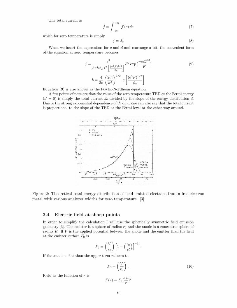
A few points of note are that the value of the zero temperature TED at the Fermi energy(ε′ = 0) is simply the total current J0 divided by the slope of the energy distribution d.Due to the strong exponential dependence of J0 on c, one can also say that the total currentis proportional to the slope of the TED at the Fermi level or the other way around.
Figure 2: Theoretical total energy distribution of field emitted electrons from a free-electronmetal with various analyzer widths for zero temperature. [3]
2.4 Electric field at sharp points
In order to simplify the calculation I will use the spherically symmetric field emissiongeometry [3]. The emitter is a sphere of radius r0 and the anode is a concentric sphere ofradius R. If V is the applied potential between the anode and the emitter than the fieldat the emitter surface F0 is
F0 =(V
r0
) [1−
(r0R
)]−1
.
If the anode is flat than the upper term reduces to
F0 =(V
r0
). (10)
Field as the function of r isF (r) = F0(
r0r
)2
6

and the potential energy at any r is
V (r) = −∫ r
r0
F (r′)dr′ = r0F0
(1− r0
r
)= V
(1− r0
r
).
As can be seen from equation (10), electric field tends to concentrate at sharp points.Since the value of the field at the emitter tip is hard to obtain unambiguously, the
combining the F-N data together with the slope of TED to obtain values for the workfunction, was suggested. The field between the emitter and the accelerating anode isdetermined by the applied voltage which is really the experimentally controllable variable.If patch fields are neglected, then the field is related to the voltage as
F = βV
with β some undetermined geometrical factor. It is further more assumed that thefield distribution over the emitter area seen in the probe hole is constant. The slope of anexperimental F-N curve ( jtot
V 2 vs 1V ) can than be given instead of the slope of ( j
F 2 vs 1F ).
3 Field emission from carbon nanotubes
3.1 Carbon nanotubes
In 1991 multi-wall nanotubes were discovered by Iijima in a carbon deposit which was lefton an electrode after the recovery of fullerene soot produced by a carbon arc [5]. Single-wallnanotubes were discovered two years later in 1993.
Carbon nanotubes are composed of either one graphene sheet rolled into cylinder(single-wall nanotube (SWNT)) or several nested cylinders (multi-wall nanotube (MWNT))with an inter layer spacing of 0.34−0.36 nm that is close to the typical spacing of graphite.The diameter of the MWNTs typically ranges from 10 to 50 nm and its length exceeds10 µm. For SWNTs the diameter in only 1 nm and its length is up to 100 µm.
In practice different varieties of nanotubes can be found [7]. There are several possibil-ities to form a cylinder with a graphene sheet. The direction in the graphene sheet planeand the nanotube diameter are represented in a pair of integers (n,m). They denote thenanotube type. Nanotubes formed from the graphene sheet rolled along the symmetryaxis are either zig-zag (n = 0 or m = 0) or armchair (n, n) type. When the direction inwhich the sheet is rolled differs from symmetry axis, the nanotube is chiral (n,m). In thiscase, the equivalent atoms of each unit cell are aligned on a spiral. In general, the wholefamily of nanotubes is classified as zig-zag, armchair and chiral tubes of different diametersFig.3. In practice no particular type is preferentially formed. In most cases, the layers ofMWNTs are chiral and of different helicities. Although these structures are closely relatedto graphite, the curvature, symmetry and small size induce marked deviations from thegraphitic behavior.
Depending on the type, the nanotubes can be (unlike graphite) metallic or semicon-ducting. All armchair SWNTs are metallic. Nanotubes with inherent (n,m) helicity andof the zig-zag variety can be either semiconducting or metallic, depending on the exactvalues of n and m.
The tubes are usually closed at both ends by fullerene-like half spheres, producing thusa well-defined tip with a very small radius of curvature, but they can have open tips aswell Fig.4. In the cap of the nanotube tip pentagons in otherwise hexagonal lattice can befound producing positive curvature of graphene layer [1]. Samples with closed and openedtips produce different emission patterns as can be observed in Fig.5.
3.2 Field emission from carbon nanotubes
The idea of the present work is to use tips of carbon nanotubes as a source of field emission[8]. They possess the following properties favorable for field emitters: a high aspect ratio,a sharp tip, high chemical stability, and high mechanical strength. Carbon nanotubeshave excellent emission characteristics such as high spatial and temporal coherence, low
7

Figure 3: Models of different nanotube structures (A) armchair, (B) zig-zag, and (C) chiral.Projections normal to the tube axis and perspective views along the tube axis are on the topand bottom, respectively. In reality this SWNTs would have had the diameter of approximately1 nm. (D) Tunneling electron microscope image showing the helical structure of a 1.3 nmdiameter SWNT in a bundle. (E) Transmission electron microscope (TEM) image of a MWNTcontaining a concentrically nested array of nine SWNTs. (F) TEM image of lateral packingof 1.4 nm diameter SWNTs in a bundle. (G) Scanning electron microscope (SEM) image ofan array of MWNTs grown as a nanotube forest. [6]
Figure 4: Images of tips for four kinds of carbon nanotubes made with transmission electronmicroscope. (a) Pristine MWNT with a capped end, pristine nanografiber (b), MWNT withan open end (c) and a bundle of purified SWNTs. Scale bars show 5 nm. [5]
operating voltages and produce high current densities and there for favorably comparewith other field emission sources.
In 1995 first field emission from s single nanotube and from a carbon film was reported.Subsequently, many experimental studies on FE from CNTs were reported.
8

Figure 5: Field emission patterns of pristine MWNTs (a), open MWNTs (b), and bundles ofSWNTs (c). [5]
Figure 6: SEM images of (a) single MWNT tip and (b) MWNT film before emission. Ex-perimental setup for field emission measurements of MWNT tips (c) and MWNT films (d).[8]
3.2.1 Field emission energy distribution and workfunction
One aspect of field emission that has not been discussed yet is the importance of theelectronic properties, more specifically of the electronic density of states (DOS), on thefield emission. In metals, the DOS of the conduction electrons, which are responsible forthe emission, is described by Fermi-Dirac statistics as we have seen in previous section[1]. The workfunction (φe) corresponds to the energy difference between the Fermi leveland the top of the surface barrier as shown in Fig.7. Above the Fermi level the tunnelingprobability increases but the DOS decreases vary sharply. Below the Fermi level The DOSincreases slightly but the tunneling probability decreases strongly. These considerationsare directly reflected in the specific shape for the field emission energy distribution (FEED)of the electrons predicted by the Fowler-Nordheim theory (see Fig.7). The FEED peaksaround the Fermi level with exponential tails that depend on the Fermi temperature ofthe electrons and on the slope of the tunneling barrier for the high and low energy tail.
9

Figure 7: Standard field emission model from a metallic emitter, showing the potential barrierand the corresponding FEED (energy on the vertical axis, current on the horizontal logarithmicaxis)[1].
Any deviation from this metallic shape is due either to adsorbates or to non-metallic DOS.FEED can therefore be used to gain information on the DOS of the emitting electrons aswell as to determine the workfunction.
The FWHM (full width at half maximum) of the FEED is typically 0.45 eV for a metal.Measurements on nanotubes consistently show that the FEED is significantly narrowerand additional features suggest that the emission is more complicated than for a metallicemitter. In the measurement below (Fig.8), the FWHM amounts to less than 0.2 eV .
From observations was concluded that the electrons are emitted from sharp energylevels due to localized states at the tube cap as shown below. Actually, theoretical calcula-tions predict the presence of localized states at the tube cap. This was recently confirmedexperimentally by STM measurements. One further element in favor of this model is theobservation of luminescence induced by the electron emission.
Figure 8: Field electron energy spectra obtained on a MWNT film (with a linear and loga-rithmic current scale for the bottom and top trace, respectively), showing a single peak, alongfits obtained with the F-N distribution (dotted line) and with the modified F-N distributionincluding a Gaussian band of states (dashed line) [10].
Such energy distributions measurements remain also the only reliable method to de-termine the workfunction of a field emitter. Experimental results on the workfunction arestill fragmentary. Fransen et al. determined a workfunction of approximately 7.3 eV onone MWNT. Kuttel et al. found a workfunction in the 5 eV range for a CVD MWNTfilm. Lovall et al. deduced a value of 5.1 eV for a single SWNT from the slope of theI − V curve, having beforehand characterized their emitter to assess reliably the field
10

amplification factor.
Figure 9: Model for the field emission from nanotubes, showing the energy bands in thedifferent part of the nanotube, the potential barrier, as well as the corresponding FEED(energy on the vertical axis, current on the horizontal logarithmic axis). Emission throughenergy bands corresponding to electronic states localized at the nanotube cap [1].
Figure 10: Model for the field emission from nanotubes, showing the energy bands in thedifferent part of the nanotube, the potential barrier, as well as the corresponding FEED(energy on the vertical axis, current on the horizontal logarithmic axis). Absorbate resonanttunneling [1].
Two points have to be mentioned concerning this hypothesis. If several energy levelsparticipate in the emission, the occupied level nearest to the Fermi energy will supplynearly all the emitted electrons. Since the position of this level would depend strongly onthe local atomic configuration (tube diameter, chirality, presence of pentagons and otherdefects), significant differences of the emitted currents can be expected from one tube toanother. Second, these localized states often show far higher carrier densities as comparedto the tube body at the Fermi level. As the field emission current depends directly on thiscarrier density, we speculate that the emitted current would be far lower for a nanotubewithout such states.
A complete study by Dean et al. suggests complementary mechanisms, and showsclearly that the emission behavior of nanotubes is far more complex than the one expectedfrom a very sharp metallic tip with a workfunction of 5 eV. Different emission regimeson single SWNTs were identified and depended on applied field and temperature. A firstregime corresponding to resonant tunneling through an adsorbate was found under ”usual”experimental conditions at low temperatures and applied fields. The involved moleculehas been identified as water and it appears that this adsorbate-assisted tunneling is thestable field emission mode at room temperature.
In short, the present understanding is that the emission involves a non-metallic DOSand/or adsorbate-resonant tunneling. Supplementary informations on the electronic struc-ture of the nanotube cap and on the influence of absorbates or bonded groups are clearlyrequired for a better comprehension of the emission.
11

It is not clear so far if the workfunction of closed MWNTs, open MWNTs or SWNTsare different. The workfunction might even be different from one tube to the next. Onecan expect a variation in workfunction between the basal plane of graphite and its openedge, as shown by simulations. Finally, ultraviolet photoelectron spectroscopy measure-ments performed on MWNT films gave a clear indication that the workfunction can varysignificantly with the surface state of the tubes. This underlines once again the uttermostimportance of emitter preparation, and shows that the properties of the tubes may besignificantly influenced by the synthesis and purification methods.
3.2.2 Single carbon nanotubes and carbon films
Carbon nanotubes can be used as electron sources in two different types of setups, namelysingle (using only one nanotube) and multiple electron beam devices (using films of carbonnanotubes) Fig.6. for single beam device individual nanotubes are mounted on the tip of aconducting fiber. CNTs stick to the tip either by van der Waals forces or by first applyingsome conductive adhesive to the tip. The first electron field emission from a single nanotubewas reported by Rinzler et al. who studied a MWNT mounted on a carbon fiber. Theemission followed roughly a F-N behavior.
Figure 11: SEM images of a cathode made of pristine MWNTs, which are fixed with silverpaste on a stainless steel plate. (a) Low-magnification image showing a columnar structurecomposed of MWNTs and (b) high-magnification image of the top of the column, showingindividual MWNTs that extrude outward. [5]
For realization of multiple electron beam devices carbon films are used. De Heer pro-duced a nanotube film emitter by drawing a colloidal suspension of MWNTs through ananopore alumina filter. This film was then transferred by pressing the filter face downon a teflon or teflon coated metal surface. It is of the same efficiency if the suspensionis sprayed on a heated surface. Nowadays nanotubes can be grown in different patternsdirectly on films Fig.11.
In comparison to usual metallic emitters, the applied voltages were far lower for acomparable emitted current. For the single tips currents of 1 µA were typically obtainedat 250 V . For the fields, it was determined Et0, the turn on voltage (electric field needed toproduce a current of 1 µAcm−2) and Ethr, the threshold voltage (current of 10 mAcm−2)
12

Figure 12: Single I − V characteristics of (a) a MWNT tip and (b) a MWNT film with insetsof the corresponding F-N plots. [8]
to compare the MWNT films with other film field emitters. Typically, it was obtainedEt0 = 2.6 V µm−1, Ethr = 4.6 V µm−1, which corresponded to the fields just above thetip of Ft0 = 4.6 V nm−1, Fthr = 6.3 V nm−1. In comparison, other film emitters showcomparable turn-on voltages, but far higher threshold voltages [8].
The emission from single nanotubes at low currents followes a Fowler-Nordheim be-havior (Fig.12) up to currents of 5− 25 nA. As the current is further incresed small slopechanges and sometimes strong saturation effects occure. It was noted that all emitters werecapable of emitting over an incredible current range. Currents up to 0.1 mA per tube werereached repeatedly on all emitters. Finally it was found that open tubes emitted at abuottwice the voltage needed for the closed ones. Carbon films show similar characteristics [1].
Considering the emission of electrons the presence of neighboring tubes and/or nanopar-ticles near the emitting tubes on the films lowered significantly the field amplification withrespect to an isolated tube, even within the uncertainty due to the arbitrary value of thework function and to the fact that a given field amplification factor can be obtained withdifferent parameter pair (a,n) [8].
The emitted current depends directly on the local electric field at the emitting surface,E, and on its workfunction, φe, as shown before. In fact, a simple model (the Fowler-Nordheim model) shows that the dependence of the emitted current on the local electricfield and the workfunction is exponential-like. As a consequence, a small variation ofthe shape or surrounding of the emitter (geometric field enhancement) and the chemi-cal state of the surface has a strong impact on the emitted current. These facts make athorough comparison of resoults delicate, particularly because the methods used for syn-thesis (SWNTs, MWNTs), purification (closed or open ends, presence of contaminatingmaterial), and film deposition (alignment, spacing between the tubes) are quite varied [1].
One interesting parameter is the actual emitter density on the films. Typically, afilm has a nanotube density of 108 − 109 cm−2. The effective number of emitting sties,
13

however, is quite lower. Typical densities of 107 − 108 emitters/cm2 were reported. Thetype of tubes has no conclusive influence on the field emission properties, but intrinsicstructural and chemical properties of the individual tubes play a role, as marked differenceswere found depending on the diameter and surface treatment as well as between closedand open tubes. The density and orientation of the tubes on the film influences alsothe emission. The comparison and interpretation of the results is difficult because mostgroups either use different experimental procedurs, vary several parameters or did notcharacterize completely their samples. It ts hence unclear whether the observed variationsin field emission properties are due to different intrinsic properties of the tubes (SWNTsas compared to MWNTs) or to the preparation method.
Figure 13: Field amplification βfilm/βtube as a function of the inter-tube distance l for a nom-inal hight h0 = 2 µm. The dashed line corresponds to the function f(l) = 1− exp (−1.1586l)obtained by fitting from the simulated values. The inset shows a typical electrostatic simula-tion of the equipotentials around an array of emitters. [9]
We will now discuss the influence of the density on the field emission obtained frompatterned samples fabricated and mesured under identical conditions. A careful study ofthe patterns revealed that the density and length of the tubes were only two parameterswhich changed from sample to sample.
Figure 14: Scanning field emission images of MWNT films of different densities acquired atconstant voltage and tip height. The grayscale represents the current intensity. Images weretaken on films with different nanotube densities: (a) low, (b) medium and (c)high [1].
The best emitter corresponds to the film shown in Fig.14(b), followed by the film inFig.14(c). The worst emitter is the film of Fig.14(a). The analysis of eleven samples ofdifferent densities [1] proved that films of medium densities with nanotubes protrudingover the film surface show emission at the lowest fields.
We may readily understand that a film of low density and short tubes will be an inef-ficient cathode. The medium density films show a very homogeneous and strong emissionwith a large number of emitting sites. A very dense film, however, shows a decreased qual-ity of the emission. This results from a combination of two effects: the intertube distanceand the number of emitters. When the intertube distance is large, the field amplificationfactor is determined only by the diameter and the height of the nanotube. As the distancebetween the tubes is decreased, screening effects become significant. Since the number of
14

emitters increases with decreasing intertube distance, there will be an optimum distancefor a maximal emitted current density 13. The calculations indicate that this distanceamounts to 1− 2 times the tube height [1].
3.2.3 Emitter degradation
It was already noted that carbon nanotubes show excellent field emission performanceswith the lowest values for turn-on and treshold fields. However, although the operationvoltage is an important parameter for applications, the key factor is long-term stability.The degradation of the emitting performances can be evaluated by measuring the evolutionof emission intensity at constant applied voltage [10].
For any future application, the prerequisite of the long-term stability of the emittingfilms must be fulfilled. The longest test up-to-date has been performed by Saito et al. whoreport an increase of 11 per cent of the applied field to maintain an emission current of10 mA/cm2 during 8000h.
Figure 15: Long-term emission stability at constant applied voltage for a closed MWNT anda SWNT film. The extent of the y axis is the same for both films [10].
Other studies show nevertheless that degradation can occur on shorter time scales. Atpresent the origin of degradation is not clear. It seems that residual gases have a significantinfluence and that the emitted current density is important as well. In addition, theintrinsic properties of nanotubes also have an importance. A comparison between filmsof SWNTs and MWNTs at comparable chamber pressure and emitted current densityshowed that the degradation was a factor of 10 faster for SWNTs. The faster degradationof SWNTs was attributed to the fact that their single shell makes them more sensitive toion bombardment and irradiation, while the multiple shells of MWNTs tend to stabilizetheir structure.
The mechanism that leads to the catastrophic failure of a single nanotube is not com-pletely understood, but some interesting hints are already available. De Heer et al. pre-sented recently some experiments of field emission on single MWNTs in a transmissionelectron microscope. It appears that tube failure occurs on a very short time scale (< 1ms)at currents above 0.1 mA and that it involves an irreversible damage to the tube. Tube lay-ers or caps are removed, peeled back, or the end of the tube is amorphized 16. In all casesa strong decrease in the emission current occurs and the voltage has to be substantiallyincreased to obtain comparable currents.
4 Applications
Considerable effort has been made to put field emission theory into practice even beforethe nanotubes were discovered. The first field emitters were realized by Spindt et al. bydepositing Mo cones on grooved Si substrates to produce emitter arrays Fig.17. Then veryhigh electric field in the order of 107 V/cm was applied on a surface and electrons inside
15

Figure 16: A series of TEM images showing the electron field emission-induced structuraldamage at the tip of carbon nanotube [11].
the solid were emitted into vacuum by the quantum mechanical tunneling effect. In orderto achieve these high fields at reasonable voltages the cathode or emitter is usually etchedto a very sharp point. Therefore, several thousand volts applied to an anode will producethe desired field at the emitter surface [1].
Figure 17: An example of so called Spindt-emitter.
Commercial flat displays based on Spindt-type emitters are available. The fabrica-tion of such cathodes involves several processing steps and the cathodes themselves areunfortunately quite sensitive to the ambient conditions. There fore ultra high vacuumis strongly recommended. Particularly the metallic cathodes are prone to interact withresidual gaseous molecules which can considerably damage the sharp point of the emitter.
Despite the fact that a single MWNT emits monochromatic electrons over a long periodof time at low applied fields, it has been used only in a low energy electron projectionmicroscope. Here electrons are extracted by applying a voltage between the sample and aMWNT emitter. The nanotube provides a highly coherent beam that allows the acquisitionof in-line electron holograms of the observed objects with a quality comparable to atomsized W emitters [1].
In contrast to single nanotube devices, applications based on an assembly of nanotubesare diverse. Nanotube flat-panel displays were proposed early on as an ”enticing” alterna-
16

Figure 18: (A) Shematic illustration of a flat panel display based on carbon nanotubes (ITO -indum tin oxide). (B) SEM image of an electron emitter for a display, showing well-separatedSWNT bundles protruding from the supporting metal base. (C) Photograph of a 5 in nanotubefield emission display made by Samsung. [6]
tive to other film emitters described above. It took only three years until the first displaywith 32×32 matrix-addressable pixels in diode configuration was realized. Since then, theSamsung group has developed a 5-inch (13-cm) nanotube field emission display Fig.18.
Figure 19: life test of a cathode-ray tube lightning element under a DC drive, a constantemission current of 210 µA, and an anode voltage of 12 kV . Temporal change in the gridvoltage under constant emission current is shown. [5]
One possibility is to use nanotubes in lighting elements, for example, to produce lightby bombarding a phosphor coated surface with electrons. Such a cathode-ray tube (”jum-botron lamp”) has been developed and is commercially available. The brightness is typi-cally higher by double as compared with conventional thermionic lightning elements andcan be used for giant outdoor displays. Lifetimes of such devices are up to 8000 h Fig.19.
Field emitters are also in great interest for microwave amplification. This type ofapplication is very demanding since it requires current density of at least 0.1 A/cm2. Aprototype was constructed based on a SWNT cathode that was able to reach that lowerlimit to operate in microwave tubes.
A gas discharge tube that serves as an overvoltage protection was also constructed.When the voltage between a nanotube cathode and a counter-electrode reaches a thresholdvalue for field emission, the emitted current induces a discharge in the noble gas-filledinter electrode gap. It was demonstrated that this device shows better performance thancommercially available elements.
17
5 Conclusion
In the recent years nanotubes have proved to be excellent field emitters. This reflectsin vast number of field emission devices that use single nanotubes or nanotube films asfield emitters. Applications with nanotube film emitters show extremely good emissionproperties – robustness, high current densities and long emitter lifetimes. Shortly, carbonnanotubes have provided possibilities in nanotechnology that were not conceived in thepast. This is mainly reflected in exponential increase in patent filings and publications oncarbon nanotubes along with growing industrial and academic interest.
At the end I would like to thank my mentor prof. dr. D. Mihailovic for help with thisseminar and some of my colleges for their support and useful suggestions.
References
[1] J.-M. Bonard, H. Kind, T. Stoeckli, L.O. Nilsson, Field emission from carbon nan-otubes: the first five years (2000)
[2] H. Suige, M. Tanemura, V. Filip, K. Takahashi, and F. Okuyama, Appl. Phys. Lett.78 (2001); 2578
[3] J.W. Gadzuk and E.W. Plummer. Rev. Modern Phys. 45 (1973); 487.
[4] R. Gomer, Field Emission and Field Ionization, Harvard University Press (1961)
[5] Y. Saito and S. Uemura, Carbon 38 (2000); 169
[6] Ray H. Baughman, Anvar A. Zakhidov, and Walt A. de Heer, Science 297 (2002); 787
[7] D. Lovall, M. Buss, E. Graugnard, R.P. Anders, R. Reifenberger, Phys. Rew. B 61(2000); 5683
[8] J.-M. Bonard, F. Maier, T. Stoeckli, A. Chatelain, W.A. De Heer, J.P. Salvetat andL. Forro. Ultramicroscopy 73 (1998); 7
[9] J.-M. Bonard, N. Weiss, H. Kind, T. Stoeckli, L. Forro, K. Kern, A. Chatelain, Adv.Mater. 13 (2001); 184
[10] J.-M. Bonard, J.-P. Salvetat, T. Stoeckli, L. Forro, A. Chatelain, Appl. Phys. A 69(1999); 245
[11] Z.L. Wang, P. Poncharal, W.A. de Heer, Microsc. Microanal. 6 (2000); 224
[12] N.S. Lee et al., Diamond Relat. Materials 10 (2001); 265
18