field effect transistors with layered two-dimensional...
TRANSCRIPT

Field effect transistors with layered two-dimensional SnS22xSex
conduction channels: Effects of selenium substitution
T. S. Pan,1,2,a) D. De,1,a) J. Manongdo,3,4 A. M. Guloy,3 V. G. Hadjiev,5 Y. Lin,2,b)
and H. B. Peng1,b)
1Department of Physics and Texas Center for Superconductivity, University of Houston, Texas 77204-5005,USA2State Key Laboratory of Electronic Thin Films and Integrated Devices, University of Electronic Science andTechnology of China, Chengdu 610054, China3Department of Chemistry and Texas Center for Superconductivity, University of Houston, Texas 77204-5003,USA4Institute of Chemistry, University of the Philippines, Diliman, 1101 Quezon City, Philippines5Department of Mechanical Engineering and Texas Center for Superconductivity, University of Houston,Texas 77204-5002, USA
(Received 22 May 2013; accepted 29 July 2013; published online 28 August 2013)
A thorough characterization of field effect transistors with conduction channels made of SnS2�xSex
nanocrystals having different selenium content is presented. The main effect of increasing the
selenium content is a suppression of the drain-source current modulation by the gate voltage. The
temperature dependence of SnS2�xSex conductivity for all compositions is characterized by an
activation energy that gradually decreases with x. A simple donor model, with parameters of SnS2
and SnSe2 deduced from density functional theory, suggests that the change in the activation
energy is mostly due to enhanced dielectric constants that accompany the band gap reduction in
SnS2�xSex. VC 2013 AIP Publishing LLC. [http://dx.doi.org/10.1063/1.4819072]
Sustaining Moore’s Law beyond silicon-based elec-
tronic devices has drawn ever-increasing attention on novel
low-dimensional materials suitable for the production of
field effect transistors (FETs), the building blocks for elec-
tronics. The discovery of graphene, a truly two-dimensional
material comprised of atomically thin layer of carbon, has
brought significant excitement and promises for novel
applications.1–5 Nevertheless, the range of application for
graphene in digital electronics is limited by its absence of a
band gap. As an alternative, other layered materials with a fi-
nite band gap such as boron nitrides, metal dichalcogenides,
and molybdenum oxide have been considered.6–9 Metal
dichalcogenides provide promising materials for wide range
of applications in areas like field effect devices,10,11 memory
devices,12 and energy storage.13,14 Among this class of mate-
rials, SnS2, a semiconductor with a band gap of 2.1 eV, was
recently shown to exhibit a high FET on/off ratio of �106,15
a feature much desirable for the next generation electronic
devices.16 Moreover, selenium doping in SnS2 offers a useful
route for bandgap engineering, in that the band gap of
SnS2�xSex can be continuously tuned from 2.1 eV (SnS2) to
1.0 eV (SnSe2) by varying the selenium content.17 This
would provide an important versatility in low-power elec-
tronic and optoelectronic devices. For example, the bandgap
of SnSe2 is very close to that of silicon (1.1 eV), and was
reported to have higher carrier mobility than SnS2 in bulk
form.18 Therefore, a systematic study of FET devices based
on nano-sized SnS2�xSex crystals as conduction channels
will be very useful for evaluating the potential of these mate-
rials in future nanoelectronics applications.
Layered tin dichalcogenides, SnS2 and SnSe2, are both
isostructural with the hexagonal CdI2 type crystal structure
and exhibit indirect band gaps.19 Their valence bands are
predominantly derived from the p orbitals of chalcogens
(sulfur and/or selenium), whereas the conduction bands are
hybridized orbitals derived from the p orbitals of the chalco-
gens (sulfur and/or selenium) and the s orbital of tin. Since
both sulfur and selenium are group VI elements, a solid solu-
tion of the isostructural tin dichalcogenides, SnS2�xSex can
be prepared. FET devices based on solution-processed gran-
ular thin films of SnS2�xSex exhibit larger current densities
and relatively higher mobility compared with its analogous
organic FETs.10 However, there has been little work done on
nano-sized crystalline SnS2�xSex as an effective conduction
channel in FETs.
In this work, we investigated field-effect transistors
based on mechanically exfoliated (11–35 nm thick)
SnS2�xSex crystals with varying selenium content, system-
atically from x¼ 0 to 2. The FET characteristics were meas-
ured with temperature varied from 90 K to 295 K, and the
activation energies are subsequently obtained as a function
of selenium doping.
In our studies, bulk SnS2�xSex single crystals were
grown by reacting the pure elements in quartz ampoules via
chemical vapor transport using iodine as transport agent,20 as
described in a previous work.15 Vacuum evacuated ampoules
loaded with source materials were heated in a two-zone fur-
nace and the as-grown crystals were transported from the hot
zone (700 �C) to the cold zone (650 �C) over 12 h.
Thereafter, the furnace was air-cooled to room temperature.
Single crystals of the tin dichalcogenides, with six different
compositions (SnS2, SnS1.6Se0.4, SnS1.2Se0.8, SnS0.8Se1.2,
SnS0.4Se1.6, and SnSe2) were prepared, and their crystal
structures were confirmed by X-ray diffraction (XRD)
a)T. S. Pan and D. De contributed equally to this work.b)Author to whom correspondence should be addressed. Electronic addresses:
[email protected] and [email protected]
0003-6951/2013/103(9)/093108/5/$30.00 VC 2013 AIP Publishing LLC103, 093108-1
APPLIED PHYSICS LETTERS 103, 093108 (2013)
(PANalytical X’Pert PRO, Cu Ka, k¼ 1.5406 A).
Subsequently, Scotch-tape method15 was employed to
mechanically exfoliate the SnS2�xSex crystals into thin nano-
crystals. The device structure schematic and an atomic force
microscope (AFM) image of a real FET device are shown in
Figs. 1(a) and 1(b). Here the gate dielectrics consists of a
200-nm-thick SiO2 layer deposited on doped Si wafer, and
the source and drain electrodes are thermally-evaporated
metal electrodes (45 nm Pd/5 nm Cr) connecting a thin
SnS2�xSex nanocrystal (the FET conduction channel). All
electrical measurements were conducted under vacuum
(�10�5–10�6 Torr) in a Lakeshore TTP6 cryogenic probe
station.
As shown in Fig. 1(c), X-ray diffraction patterns of our
SnS2 and SnSe2 samples can be indexed with hexagonal unit
cells of the CdI2-type, consistent with those reported.21,22
For the solid solution compositions, the SnS2�xSex crystals
also retain the CdI2 structure type. As expected for a larger
atomic radius of Se, the lattice constants determined from
the XRD data increase with increasing Se content.
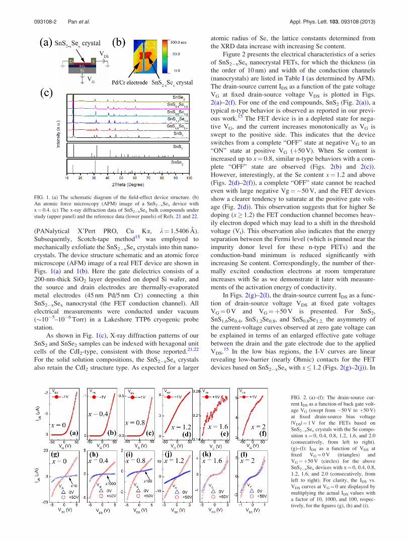
Figure 2 presents the electrical characteristics of a series
of SnS2�xSex nanocrystal FETs, for which the thickness (in
the order of 10 nm) and width of the conduction channels
(nanocrystals) are listed in Table I (as determined by AFM).
The drain-source current IDS as a function of the gate voltage
VG at fixed drain-source voltage VDS is plotted in Figs.
2(a)–2(f). For one of the end compounds, SnS2 (Fig. 2(a)), a
typical n-type behavior is observed as reported in our previ-
ous work.15 The FET device is in a depleted state for nega-
tive VG, and the current increases monotonically as VG is
swept to the positive side. This indicates that the device
switches from a complete “OFF” state at negative VG to an
“ON” state at positive VG (þ50 V). When Se content is
increased up to x¼ 0.8, similar n-type behaviors with a com-
plete “OFF” state are observed (Figs. 2(b) and 2(c)).
However, interestingly, at the Se content x¼ 1.2 and above
(Figs. 2(d)–2(f)), a complete “OFF” state cannot be reached
even with large negative Vg¼�50 V, and the FET devices
show a clearer tendency to saturate at the positive gate volt-
age (Fig. 2(d)). This observation suggests that for higher Se
doping (x� 1.2) the FET conduction channel becomes heav-
ily electron doped which may lead to a shift in the threshold
voltage (Vt). This observation also indicates that the energy
separation between the Fermi level (which is pinned near the
impurity donor level for these n-type FETs) and the
conduction-band minimum is reduced significantly with
increasing Se content. Correspondingly, the number of ther-
mally excited conduction electrons at room temperature
increases with Se as we demonstrate it later with measure-
ments of the activation energy of conductivity.
In Figs. 2(g)–2(l), the drain-source current IDS as a func-
tion of drain-source voltage VDS at fixed gate voltages
VG¼ 0 V and VG¼þ50 V is presented. For SnS2,
SnS1.6Se0.4, SnS1.2Se0.8, and SnS0.8Se1.2, the asymmetry of
the current-voltage curves observed at zero gate voltage can
be explained in terms of an enlarged effective gate voltage
between the drain and the gate electrode due to the applied
VDS.15 In the low bias regions, the I-V curves are linear
revealing low-barrier (nearly Ohmic) contacts for the FET
devices based on SnS2�xSex with x� 1.2 (Figs. 2(g)–2(j)). In
FIG. 1. (a) The schematic diagram of the field-effect device structure. (b)
An atomic force microscopy (AFM) image of a SnS2�xSex device with
x¼ 0.4. (c) The x-ray diffraction data of SnS2�xSex bulk compounds under
study (upper panel) and the reference data (lower panels) of Refs. 21 and 22.
FIG. 2. (a)–(f): The drain-source cur-
rent IDS as a function of back gate volt-
age VG (swept from �50 V to þ50 V)
at fixed drain-source bias voltage
|VDS|¼ 1 V for the FETs based on
SnS2�xSex crystals with the Se compo-
sition x¼ 0, 0.4, 0.8, 1.2, 1.6, and 2.0
(consecutively, from left to right).
(g)–(l): IDS as a function of VDS at
fixed VG¼ 0 V (triangles) and
VG¼þ50 V (circles) for the above
SnS2�xSex devices with x¼ 0, 0.4, 0.8,
1.2, 1.6, and 2.0 (consecutively, from
left to right). For clarity, the IDS vs.
VDS curves at VG¼ 0 are displayed by
multiplying the actual IDS values with
a factor of 10, 1000, and 100, respec-
tively, for the figures (g), (h) and (i).
093108-2 Pan et al. Appl. Phys. Lett. 103, 093108 (2013)

contrast, for the FET devices with higher selenium concen-
trations (SnS0.4Se1.6 and SnSe2), a non-linear I-V behavior is
observed (Figs. 2(k) and 2(l)), which could be attributed to
stronger Schottky barriers at the metal-semiconductor con-
tacts. We note that this nonlinear I-V behavior is reproduci-
bly observed in other FET devices with x¼ 1.6 and x¼ 2.0
and thus a higher Schottky barrier may be an intrinsic behav-
ior for these doping levels. This could be related to the shift
of the Fermi level in the high Se-content materials which can
affect the formation of Schottky barrier, or due to the effect
of surface states that influences the formation of Schottky
barriers. We also note that the absolute magnitude of IDS
varies for devices shown in Fig. 2, because IDS can be
affected by many factors such as the contact barrier height,
the detailed geometry of the SnS2�xSex crystal for each de-
vice, or a change in carrier density.
The I-V curves at gate voltage VG¼ 0 V were also char-
acterized with temperature varied from 90 K to 295 K, as
shown in Figure 3. All SnSxSe2�x-based devices become
less conductive with decreasing temperature, which is mostly
due to the reduction of the number of thermally excited car-
riers. The conductivity activation energy, Ea, of the semicon-
ducting FET channels can be determined from the
temperature dependence of drain-source resistance, R, as
given by the Arrhenius equation
R ¼ R0eEa=kBT ; (1)
where the R0 is a pre-exponential constant factor, kB is the
Boltzmann constant, and T is the measurement temperature.
The drain-source resistance R at different temperatures is
determined by linear fitting of corresponding I-V curves at
VDS¼�1 V. The relationship of the FET channel composi-
tion with the obtained activation energy is plotted in
Fig. 4(a).
The activation energy in a semiconductor can be
expressed as
Ea ¼ Ec � EF; (2)
where Ec is the conduction band minimum and EF is the
Fermi level. A comparison of the band gaps of the end-
members, SnS2 (2.1 eV) and SnSe2 (1.0 eV), yields activation
energies that are 1/15 th (SnS2) and 1/54 th (SnSe2) of their
respective band gaps. This observation suggests that the
Se-doping in SnS2�xSex leads to shallow donor impurities
and the conductivity activation energy Ea should then be
equal to the donor ionization energy, Ed.
The simplest approach of calculating the ionization
energies of shallow donors is to use a modified hydrogen-
like model of impurities.23 The energy of the first excited
state Ed of an electron around a donor impurity is given by
Ed ¼ �13:6
e2r
m�cm0
eV; (3)
where m�c is the effective mass of electron in the lowest conduc-
tion band, m0 is that of a free electron at rest, and er is the rela-
tive dielectric constant of the crystal host. Although Ref. 24
reports a conductivity effective mass m�c ¼ ð0:4 6 0:2Þm0 for
SnSe2 deduced from far-IR absorption measurements, there are
no reports on directly measured m* and er for both SnS2 and
SnSe2. Kramers-Kronig analysis of IR spectra of SnSe225 yields
a static dielectric constant of erð0Þ ¼ 21:5. Relevant data for
SnS2 are even scarcer. To overcome the lack of data needed for
the estimation of ionization energies we performed density
functional theory (DFT) calculations on the electronic band
structure and dielectric properties of SnS2 and SnSe2.
DFT calculations on SnS2 and SnSe2 were performed
using the generalized-gradient approximation (GGA) with
Perdew-Wang (PW91) exchange-correlation functional, and
the norm-conserved pseudopotential plane-waves as imple-
mented in the Quantum Espresso suite.26 The electronic
band structure, related properties, and geometry optimization
TABLE I. The thickness and width of SnS2�xSex nanocrystals for the devi-
ces of Figs. 2 and 3.
Compounds Thickness (nm) Width (lm)
SnS2 16 1.8
SnS1.6Se0.4 11 2.4
SnS1.2Se0.8 35 5.1
SnS0.8Se1.2 25 2.3
SnS0.4Se1.6 28 1.7
SnSe2 25 1.3
FIG. 3. IDS vs. VDS curves with VG¼ 0 V measured at temperatures from
90 K to 295 K for the SnS2�xSex based FETs with x¼ 0, 0.4, 0.8, 1.2, 1.6,
and 2.0 (consecutively, from (a) to (f)). Some curves at lower temperatures
are nearly overlapping and indistinguishable in the plots. We note that low
temperature experiments sometimes change the absolute value of IDS signifi-
cantly in such nano-scale FET devices, e.g., as can be seen from the data of
Fig. 2(l) measured just before the cool down and those of Fig. 3(f) in the end
of the low temperature experiment for the composition x¼ 2, probably due
to changes in surface adsorption under different vacuum conditions and
trapped charge states. However, the shape of IV curves is reproducible
before and after the low temperature experiments for all compositions by
comparing Figs. 2 and 3.
093108-3 Pan et al. Appl. Phys. Lett. 103, 093108 (2013)

of the structures were calculated self-consistent (SCF) with
100 Ry kinetic energy cutoff for the plane wave, 400 Ry
charge density cut-off, and SCF tolerance better than 10�8.
The DFT calculations yield an in-plane dielectric constant of
er ¼ 21:8 for SnSe2 that is surprisingly close to the experi-
mental value reported in Ref. 25. This gives us confidence
that the DFT value of er ¼ 10:3 for SnS2 is reliable. More
details on the DFT calculations on SnS2 and SnSe2 including
phonons and lattice strain evolution in the mixed SnS2�xSex
crystals are given in Ref. 27.
Fig. 4(b) presents the DFT electronic band dispersion
curves along the high symmetry lines in the hexagonal
Brillouin zone of SnS2 (solid line) and SnSe2 (solid circles).
Here the Fermi energy (EF¼ 0 eV) is set at the top of the va-
lence band. The DFT values for the calculated indirect gaps
of SnS2 and SnSe2 are 2.12 eV and 1.1 eV, respectively.
These values are in good agreement with experiments.17
Since the bottom of conduction band is at M-L (U-symmetry
line), we focus on the isoenergy surfaces around the M and L
points in k-space, as well as and along the U-line. The isoe-
nergy surfaces in SnS2 are found to be cylindrical, with axes
along the U-line. This means that the electron effective mass
at the bottom of conduction band of SnS2, is highly aniso-
tropic with a very large longitudinal component m�l � m0
along M-L (or the c-axis) and a transversal (in-plane) com-
ponent m�t ¼ 1:097 m0. For SnSe2, the anisotropy is weaker
and one finds m�l ¼ 1:571 m0 and m�t ¼ 0:732 m0. Having
considered the anisotropy of SnS2 and SnSe2, the conductiv-
ity effective mass m�c is then given by
m�c ¼ 31
m�lþ 2
m�t
� ��1
: (4)
Using Eq. (4), the calculated DFT conductivity effective
masses are 1:646 m0 (SnS2) and 0:889 m0 (SnSe2). Therefore,
the corresponding donor ionization energies calculated with
Eq. (3) are 210 meV and 25.5 meV for SnS2 and SnSe2,
respectively. The above calculated values for Ed (which is
equal to Ea) are consistent with the experimentally observed
trend of decreasing excitation energy Ea with increasing se-
lenium composition (x) (Fig. 4(a)). However the theoretical
values seem to overestimate those measured in this work.
From these estimates we can conclude, without making
DFT calculations for the mixed SnS2�xSex, that these com-
pounds inherently contain donor impurities, either S(Se)
vacancies or possibly iodine atoms (accompanying the
chemical vapor transport crystal growth). Donor ionization
energies depend mostly on the dielectric properties of the
host crystal, which in turn reflect the band structure and
specifically the band gap. As the band gap decreases, the
screening of electric field is attenuated, and the ionization
energy of the same type donor impurities decreases.
In summary, the field-effect devices were fabricated
using thin crystals of tin dichalcogenides SnS2�xSex with
varying Se-content (x). Increasing Se content results in a
reduction of the band gap. This is accompanied by an
increase in dielectric constant and a corresponding decrease
of the donor ionization energy. The Fermi energy is shifted
closer to the conduction band minimum (i.e., the activation
energy Ea decreases) as the Se composition is increased, and
thus the drain-source current modulation is suppressed. This
study will be instructive and useful for future application of
tin dichalcogenides in nanoelectronics.
This work was supported by the National Science
Foundation (ECCS-1247874 monitored by Anupama Kaul),
and the State of Texas through the Texas Center for
Superconductivity (TcSUH) at the University of Houston.
J.M. and A.M.G. also acknowledge the support from the R.
A. Welch Foundation (E-1297).
1K. S. Novoselov, A. K. Geim, S. V. Morozov, D. Jiang, Y. Zhang, S. V.
Dubonos, I. V. Grigorieva, and A. A. Firsov, Science 306, 666 (2004).2K. S. Novoselov, A. K. Geim, S. V. Morozov, D. Jiang, M. I. Katsnelson,
I. V. Grigorieva, S. V. Dubonos, and A. A. Firsov, Nature 438, 197 (2005).3A. K. Geim and K. S. Novoselov, Nature Mater. 6, 183 (2007).4A. H. C. Neto, F. Guinea, N. M. R. Peres, K. S. Novoselov, and A. K.
Geim, Rev. Mod. Phys. 81, 109 (2009).5C. Soldano, A. Mahmood, and E. Dujardin, Carbon 48, 2127 (2010).6K. S. Novoselov, D. Jiang, F. Schedin, T. J. Booth, V. V. Khotkevich,
S. V. Morozov, and A. K. Geim, Proc. Natl. Acad. Sci. U.S.A. 102, 10451
(2005).7A. Ayari, E. Cobas, O. Ogundadegbe, and M. S. Fuhrer, J. Appl. Phys.
101, 014507 (2007).8Q. H. Wang, K. Kalantar-Zadeh, A. Kis, J. N. Coleman, and M. S. Strano,
Nat. Nanotechnol. 7, 699 (2012).9S. Balendhran, J. Deng, J. Z. Ou, S. Walia, J. Scott, J. Tang, K. L. Wang,
M. R. Field, S. Russo, S. Zhuiykov, M. S. Strano, N. Medhekar, S. Sriram,
M. Bhaskaran, and K. Kalantar-zadeh, Adv. Mater. 25, 109 (2013).10D. B. Mitzi, L. L. Kosbar, C. E. Murray, M. Copel, and A. Afzali, Nature
428, 299 (2004).11H. T. Yuan, M. Toh, K. Morimoto, W. Tan, F. Wei, H. Shimotani, C.
Kloc, and Y. Iwasa, Appl. Phys. Lett. 98, 012102 (2011).12T. Kyratsi, K. Chrissafis, J. Wachter, K. M. Paraskevopoulos, and M. G.
Kanatzidis, Adv. Mater. 15, 1428 (2003).13S.-G. Hur, E.-T. Kim, J.-H. Lee, G.-H. Kim, and S.-G. Yoon, J. Vac. Sci.
Technol. B 26, 1334 (2008).14B. Li, J. Liu, G. Xu, R. Lu, L. Feng, and J. Wu, Appl. Phys. Lett. 101,
153903 (2012).15D. De, J. Manongdo, S. See, V. Zhang, A. Guloy, and H. Peng,
Nanotechnology 24, 025202 (2013).16International Technology Roadmap for Semiconductors (ITRS), Emerging
Research Devices (ERD), 2011 edition, 2012.17C. Julien, M. Eddrief, I. Samaras, and M. Balkanski, Mater. Sci. Eng., B
15, 70 (1992).
FIG. 4. (a) Activation energy at zero
gate voltage as a function of selenium
compositions (obtained by fitting the
Arrhenius equation). (b) DFT calcu-
lated energy band structure of SnS2
(solid line) and SnSe2 (solid circles).
093108-4 Pan et al. Appl. Phys. Lett. 103, 093108 (2013)

18G. Perluzzo, S. Jandl, M. Aubin, and P. E. Girard, Solid State Commun.
27, 1437 (1978).19R. H. Williams, R. B. Murray, D. W. Govan, J. M. Thomas, and E. L.
Evans, J. Phys. C 6, 3631 (1973).20F. A. S. Al-Alamy and A. A. Balchin, J. Cryst. Growth 38, 221 (1977).21J. R. Guenter and H. R. Oswald, Naturwiss. 55, 177 (1968).22B. Palosz and E. Salje, J. Appl. Crystallogr. 22, 622 (1989).23C. Kittel, Introduction of Solid State Physics, 4th ed. (John Wiley & Sons,
New York, 1986), p. 206.24P. A. Lee and G. Said, J. Phys. D: Appl. Phys. 1, 837 (1968).
25Landolt-B€ornstein—Group III, Condensed Matter (Springer, 1998), Vol.
41C, pp. 1–6.26G. Paolo, B. Stefano, B. Nicola, C. Matteo, C. Roberto, C. Carlo, C. Davide,
L. C. Guido, C. Matteo, D. Ismaila, C. Andrea Dal, G. Stefano de, F.
Stefano, F. Guido, G. Ralph, G. Uwe, G. Christos, K. Anton, L. Michele,
M.-S. Layla, M. Nicola, M. Francesco, M. Riccardo, P. Stefano, P. Alfredo,
P. Lorenzo, S. Carlo, S. Sandro, S. Gabriele, P. S. Ari, S. Alexander, U.
Paolo, and M. W. Renata, J. Phys. Condens. Matter 21, 395502 (2009).27V. G. Hadjiev, D. De, H. B. Peng, J. Monongdo, and A. M. Guloy, Phys.
Rev. B 87, 104302 (2013).
093108-5 Pan et al. Appl. Phys. Lett. 103, 093108 (2013)