ferromagnetism in wide band gap materials: mn-zno
TRANSCRIPT


FERROMAGNETISM IN WIDE BAND GAP MATERIALS:
Mn-ZnO AND Mn-Si3N4 THIN FILMS
(Ferromagnetismo en Materiales de Gap Ancho: Láminas Delgadas de Mn-ZnO y Mn-Si3N4)
Memoria presentada para optar al grado de Doctora en Física por:
EVA CÉSPEDES MONTOYA
Tesis dirigida por:
Prof. Carlos Prieto de Castro
Tutora:
Prof. Luisa E. Bausá López
Departamento de Física de Materiales
Facultad de Ciencias
Universidad Autónoma de Madrid
Instituto de Ciencia de Materiales de Madrid
Consejo Superior de Investigaciones Científicas
Septiembre de 2009


Summary
This dissertation is the result of a four-year doctorate on the ferromagnetism of
Mn-based wide band gap thin film materials prepared by sputtering, performed at the
Instituto de Ciencia de Materiales de Madrid (ICMM) under the supervision of Prof.
Carlos Prieto.
The first part of this work is aimed at the study of the Mn-ZnO system. The
interface-related properties as well as the influence of the particular manganese oxidation
process during growth in the ferromagnetism of this system are analysed.
The second part deals with the novel Mn-Si3N4 system, which has been firstly
studied here, reporting room temperature ferromagnetism. The origin of its
ferromagnetism is ascribed to the stabilization of a slightly distorted Mn3N2 phase, one of
the main contributions of this research.
Finally, the work is completed with investigations of the Au nanoparticles growth
in both ZnO and Si3N4 matrix materials.
Keywords: wide band gap semiconductors, diluted magnetic semiconductors, DMS,
ferromagnetic oxides, ferromagnetic nitrides, multilayers, thin films, sputtering, XAS,
XANES, EXAFS, II-VI semiconductors, MnZnO, interface, Mn oxidation state,
manganese nitride, Mn3N2, gold nanoparticles.

Resumen
El trabajo presentado en esta memoria de Tesis Doctoral se centra en el estudio
del ferromagnetismo en materiales de gap ancho preparados en forma de lámina delgada
mediante la técnica de sputtering.
La primera parte de la memoria está dedicada al estudio del sistema Mn-ZnO. Se
analizan varios factores relacionados con el ordenamiento ferromagnético del sistema,
como el papel que juegan las distintas intercaras y el efecto de la oxidación o reducción
del manganeso durante el proceso de crecimiento.
En la segunda parte de la memoria se investiga el sistema Mn-Si3N4, que ha sido
estudiado por primera vez en este trabajo y en el que se ha observado ferromagnetismo a
temperatura ambiente. El origen del ferromagnetismo en este sistema se ha explicado por
la existencia de una fase de tipo Mn3N2 ligeramente distorsionada.
Finalmente, el trabajo se completa con el estudio de la formación de
nanopartículas de Au en ambas matrices, ZnO and Si3N4.
Palabras clave: semiconductores de gap ancho, semiconductores magnéticos diluidos,
DMS, óxidos ferromagnéticos, nitruros ferromagnéticos, multicapas, láminas delgadas,
sputtering, XAS, XAS, XANES, EXAFS, semiconductores II-VI, MnZnO, intercara, estado
de oxidación de Mn, nitruro de manganeso, Mn3N2, nanopartículas de Au.

As a result of the work described in this dissertation, the following papers have
been published:
Correlation between Mn oxidation state and magnetic behaviour in Mn/ZnO multilayers prepared by sputtering. E. Céspedes, J. Garcia-Lopez, M. García-Hernández, A. de Andrés and C. Prieto, J. Appl. Phys. 102, 033907 (2007).
High temperature ferromagnetism in Mn based multilayers of wide gap semiconductors:
Mn/ZnO and Mn/SnO2: the role of interfaces. A. Espinosa, E. Céspedes, C. Prieto, M. García-Hernández and A. de Andrés, J. Korean Phys. Soc 52, 5 (2008).
Mn local order in room-temperature ferromagnetic Mn/ZnO multilayers.
E. Céspedes, G. R. Castro, F. Jiménez-Villacorta, A. de Andrés and C. Prieto, J. Phys.: Condens. Matter 20, 095207 (2008).
X-ray absorption and magnetic circular dichroism characterization of a novel
ferromagnetic MnNx phase in Mn-Si3N4 multilayers. E. Céspedes, Y. Huttel, L. Martínez, A. de Andrés, J. Chaboy, M. Vila, N. D. Telling, G. van der Laan and C. Prieto, Appl. Phys. Lett. 93, 252506 (2008).
Evolution of ferromagnetism with sputtering gas in Mn:ZnO films.
E. Céspedes, J. Sánchez-Marcos, J. García-López and C. Prieto, J. Magn. Magn. Mater.(2009), doi:10.1016/j.jmmm.2009.05.038.
Induced ferromagnetism in Mn3N2 phase embedded in Mn/Si3N4 multilayers. E. Céspedes, E. Román, Y. Huttel, J. Chaboy, F. J. García-López, A. de Andrés and C. Prieto, J. Appl. Phys. 106, 043912 (2009).
Au layer growth on amorphous Si3N4. E. Céspedes, D. Babonneau, O. Lyon, S. Rouzière, C. Prieto, L. Olivi and A. Tra-verse, J. Appl. Phys. (2009) (submitted).
Additional publications in different related fields are:
Brillouin Light Scattering Characterization of the Surface Acoustic Waves Velocity in the ZnO/ Si3N4/Si(100) System. E. Céspedes, R. J. Jiménez-Riobóo, M. Vila and C. Prieto, Superlattices and Microstructures 39, 75 (2006).
Interface and Mn valence effects in ferromagnetic insulating multilayers based on Mn and tin oxide. A. Espinosa, E. Céspedes, C. Prieto, M. García-Hernández, J. Rubio-Zuazo and A. de Andrés, J. Appl. Phys. 103, 07D129 (2008).
Microstructural properties and local order around iron in granular metal-insulator Fe/Si3N4 granular systems prepared by magnetron sputtering. F. Jiménez-Villacorta, E. Céspedes, M. Vila, A. Muñoz-Martín, G. R. Castro and C. Prieto, J. Phys. D: Appl. Phys. 41, 205009 (2008).
Neutron diffraction and X-ray absorption spectroscopy study of complex oxygen deficient manganites. R. Cortés-Gil, M. Hernando, M. L. Ruiz-González, E. Céspedes, C. Prieto, J. M. Alonso, M. Vallet-Regí, A. Hernando, J. M. González-Calbet, Chemistry-A European Journal 14, 9038 (2008).

A mi madre
A la memoria de mi padre


“Ciencia es aquello sobre lo cual cabe siempre discusión”
José Ortega y Gasset


Contents
1. Introduction …………………………………………………………………..1
1.1. State of the art …………………………………………………………….1 1.2. Outlook of this dissertation ………………………………………………..6 1.3. Dissertation structure ……………………………………………………..7
2. Thin Film Preparation Method and Experimental Techniques ……………..13
2.1. Sputtering technique ……………………………………………………..13 2.1.1. Experimental equipment …………………………………………..17
2.2. SQUID magnetometry …….…………………………………………...20 2.3. X-Ray Diffraction (XRD) ………………………………………………...21 2.4. X-Ray Reflectivity (XRR) ………………………………………………..22 2.5. Rutherford Backscattering Spectroscopy (RBS) …………………………...25 2.6. X-ray Absorption Spectroscopy (XAS) …………………………………...26
2.6.1. XAS experiments at the Mn and Zn K -edges ……………………….27 2.6.1.1. X-Ray Absorption Near-Edge Structure (XANES) ………...28 2.6.1.2. Extended X-Ray Absorption Fine Structure (EXAFS) ……...29
2.6.2. XAS at the Mn L3,2 –edge …………………………………………..31 2.6.3. X-ray Magnetic Circular Dichroism (XMCD) ……………………...34
I. Mn-ZnO system
3. Mn/ZnO Multilayers …………………………………………………….......41
3.1. Motivation ……………………………………………………………….41 3.2. Preparation of multilayers ………………………………………………...42 3.3. Magnetic properties ……………………………………………………...43 3.4. X-Ray Reflectivity (XRR) ………………………………………………...46 3.5. Rutherford Backscattering Spectroscopy (RBS) ……………………….…..50 3.6. X-Ray Diffraction (XRD) …………………………………………….…...53 3.7. Transmission Electron Microscopy (TEM) ……………………………….58

3.8. X-Ray Absorption Spectroscopy (XAS) …………………………………...61 3.8.1. X-Ray Absorption Near-Edge Structure (XANES) ………………...61 3.8.2. Extended X-Ray Absorption Fine Structure (EXAFS) ……………...63
3.9. Structural and magnetic scheme …………………………………………..72 3.10. Conclusions ……………………………………………………………..76
4. MnOx/ZnO Multilayers ……………………………………………………..81
4.1. Motivation ……………………………………………………………….81 4.2. Preparation of multilayers ………………………………………………...81 4.3. Magnetic properties ...……………………………………………………82 4.4. Rutherford Backscattering Spectroscopy (RBS) …………………………..83 4.5. X-Ray Reflectivity (XRR) ………………………………………………...85 4.6. X-Ray Diffraction (XRD) …………………………………………………86 4.7. X-Ray Absorption (XAS) ...………………………………………………88
4.7.1. XANES at the Mn K-edge …………………………………………89 4.7.2. XAS at the Mn L3,2-edge …………………………………………...90
4.8. Thermal post-deposition annealing ……………………………………….91 4.9. Discussion and remarks: The origin of FM in MnOx/ZnO multilayers versus
the origin in the so-called Mn/ZnO multilayers …………………………...92 4.10. Conclusions ……………………………………………………………...98
5. Mn:ZnO Thin Films ………………………………………………………..101
5.1. Motivation ……………………………………………………………...101 5.2. Preparation of Mn:ZnO films …………………………………………...102 5.3. X-Ray Reflectivity (XRR) ……………………………………………….104 5.4. Rutherford Backscattering Spectroscopy (RBS) …………………………106 5.5. X-Ray Diffraction (XRD) ……………………………………………….107 5.6. Magnetic properties …………………………………………………….109 5.7. X-Ray Absorption Near-Edge Structure (XANES) ………………………111 5.8. UV-VIS Absorption ……………………………………………………..115 5.9. Conclusions ...………………………………………………………….117

A. Effect of Thermal Treatments and Substrate Temperature on Mn/ZnO
Multilayers …………………………………………………………………121 B. ZnO Crystal Structures …………………………………………………….141
II. Mn-Si3N4 system 6. Mn/Si3N4 Multilayers ……………………………………………………...147
6.1. Motivation ……………………………………………………………..147 6.2. Preparation of multilayers ………………………………………………149 6.3. X-Ray Reflectivity (XRR) ………………………………………………150 6.4. Transmission Electron Microscopy (TEM) ……………………………..153 6.5. Rutherford Backscattering Spectroscopy (RBS) and Nuclear Reaction
Analysis (NRA) ………………………………………………………...154 6.6. Magnetic properties ……………………………………………………156 6.7. X-Ray Photoemission Spectroscopy (XPS) ……………………………...159 6.8. X-Ray Absorption Spectroscopy (XAS) ………………………………....162
6.8.1. X-Ray Absorption Near-Edge Structure (XANES) ………………..162 6.8.2. Computational methods: XANES simulations ……………………163 6.8.3. Extended X-Ray Absorption Fine Structure (EXAFS) …………….168 6.8.4. XAS at the Mn L3,2-edge and XMCD ……………………………..172
6.9. Remarks and discussion …….…………………………………………...174 6.10. Conclusions ……………………………………………………………177
C. From Ferromagnetism to Noble Metal Nanoparticles Formation in Si3N4 and
ZnO Systems
C.1. Au/Si3N4 Multilayers .....................................................................................................183
C.1.1. Motivation ...............................................................................................................183 C.1.2. Preparation of samples ..........................................................................................185 C.1.3. X-Ray Reflectivity (XRR) .....................................................................................186 C.1.4. Rutherford Backscattering Spectroscopy (RBS) .............................................188 C.1.5. X-Ray Absorption Spectroscopy (XAS) ............................................................190
C.1.5.1. X-Ray Absorption Near-Edge Structure (XANES) .........................190

C.1.5.2. Extended X-Ray Absorption Fine Structure (EXAFS) ....................191 C.1.6. Grazing Incidence Small Angle X-ray Scattering (GISAXS) .........................193 C.1.7. UV-VIS Absorption ................................................................................................198 C.1.8. Conclusions ..............................................................................................................203
C.2. Au/ZnO Multilayers .......................................................................................................207
C.2.1. Motivation ...............................................................................................................207 C.2.2. Preparation of samples ...........................................................................................207 C.2.3. X-Ray Reflectivity (XRR) ......................................................................................209 C.2.4. Rutherford Backscattering Spectroscopy (RBS) ..............................................212 C.2.5. X-Ray Absorption Spectroscopy (XAS) .............................................................213
C.2.5.1. X-Ray Absorption Near-Edge Spectroscopy (XANES) ..................213 C.2.5.2. Extended X-Ray Absorption Fine Structure (EXAFS) ....................213
C.2.6. X-Ray Diffraction (XRD) ......................................................................................215 C.2.7. Grazing Incidence Small Angle X-ray Scattering (GISAXS) .........................218 C.2.8. UV-vis Absorption ..................................................................................................221 C.2.9. Conclusions ..............................................................................................................223
General Conclusions ……………………………………………………………225 Agradecimientos ………….……………………………………………………..233
1
1.1. State of the art
The theoretical prediction and observation of room temperature ferromagnetism
(RTFM) in doped transition metal semiconductors is one of the most interesting and
provocative scientific developments of the early 21st century.1
The most common approach to drive a semiconductor ferromagnetic is that of
diluted magnetic semiconductors (DMSs). DMSs refer to materials obtained by doping a
non-magnetic semiconductor with a few atomic percent of transition metal (TM)
elements (e.g. V, Cr, Mn, Fe, Co, Ni and Cu), including TM-doped III-V (GaAs, InAs),
II-VI (CdTe) or group IV (Ge and Si) types. In an actual DMS, TM cations are
randomly distributed inside the semiconductor lattice, replacing a fraction of the cations
of the host. In these materials, the presence of the 3d magnetic ions influences the free
carrier behaviour through the sp-d exchange interaction between the localized magnetic
moments and the spins of the itinerant carriers, which are introduced either by the
magnetic dopant or by some secondary electronic dopant.1,2,3
DMSs are promising materials for applications as well as interesting from the
basic-physics point of view. Possible applications exist in spin electronics (spintronics),
which employ the spin degree of freedom of electrons in addition to their charge. This
may allow the integration of data processing and magnetic storage on a single device
called “spintronic device”. This new class of spintronics devices includes spin-valves,
transistors, spin light emitting diodes, non-volatile memories, magnetic sensors, etc.1,4
Since the electronic spin is a quantum mechanical degree of freedom, the exploit of
quantum interference effects in these devices could eventually lead to the design of
quantum computers. The search of new materials becomes essential for both
CChhaapptteerr 11
Introduction

CChhaapptteerr 11
fundamental research and practical applications.2,5
However, most DMSs have a low Curie temperature (TC), which totally limits
their use in practical applications. In 2000, Dietl. et al.6 employed the original Zener
model of ferromagnetism7 to theoretically predict stable ferromagnetism and TC values
that exceeded room temperature (RT) for DMSs based on wide band gap
semiconductors, i.e., ZnO and GaN, containing 5% of Mn and high hole concentration
(3.5x1020 cm-3). In addition, using first-principle calculations, Sato et al.8 theoretically
showed that a ZnO matrix doped with TM atoms such as V, Cr, Fe, Co and Ni exhibited
FM ordering, whereas doping with Ti and Cu resulted in a paramagnetic state, what
opened a window for experimental attempts to prepared DMSs with RTFM.
Since the appearance of the Diet. et al.6 publication, remarkable progress has been
made on the realization of materials with TC values above RT.
Ferromagnetic semiconductors with O2- anions, such as TM-doped ZnO, TiO2 or
SnO2 are also termed diluted magnetic oxides (DMOs).
Oxide semiconductors have many advantages in comparison with non-oxide
semiconductors: i) wide band gap suitable for short wavelength light applications, ii)
transparency and simple colouring with pigments, iii) high n-type carrier concentrations,
iv) capability to be grown at low temperatures even on plastic substrates, v) ecological
safety and durability and vi) low cost. In addition, strong electronegativity of oxygen is
expected to produce strong p-d exchange coupling between band carriers and localized
spins, pointed as an important characteristic of DMS. 9
There are two major criteria for selecting the most promising materials for
semiconductor spintronics. First, as it has been mentioned, the FM should be retained at
practical temperatures, that is, above 300 K, and second, it is a major advantage if there is
existing technology for the material in other applications. Fortunately, TM-doped ZnO
satisfies the two criteria. TM-doped ZnO has been intensively investigated in the last
years to achieve RTFM and promising magneto-transport properties.1,2,3,10 As a low cost,
wide band gap (Eg = 3.37 eV) semiconductor, ZnO itself has been focus of renewed

Introduction
3
research applications such as UV light emitters, transparent high-power electronics,
surface acoustic-wave devices, piezoelectric transducers and solar cells.3
So far, RTFM has been reported in ZnO samples doped with TM elements such as
Sc,11,12 Ti,11,13 V,14 Cr,11,15,16 Mn,17,18,19,20,21,22,23,24 Fe,25,26 Co,11,27,28,29,30 Ni31 and Cu32,33 for
which Mn- and Co-doped ZnO are the most popular systems.
In particular, the doping of ZnO with Mn is of special interest because Mn2+ has
the highest possible magnetic moment with the 3d band with 5 electrons among the 10
available states, creating a stable fully polarized state.10 Furthermore, Mn metal is not
ferromagnetic; it is well known to be antiferromagnetic as well as the standard
manganese oxides (MnO, Mn2O3 and MnO2) except Mn3O4 which is ferrimagnetic with
TC about 45 K,10 what allows to discard RTFM due to the this type of precipitates in this
system.
The rapid increase of the works around the world dealing with DMSs makes very
difficult to summarize the progress in these multi-functional materials. Nonetheless, it
should be noted that despite the large exploration performed in this field up to now, the
fundamental scientific issues in these materials are still many:
First, observations of RTFM in transition metal doped oxide semiconductors are
numerous. However, in spite of the great efforts, there is no firm conclusion whether
ferromagnetism is an intrinsic material property or comes from the clustering of
magnetic impurities, formation of secondary ferromagnetic phases, etc. Furthermore,
evidences of RTFM haven been recently reported even in undoped ZnO.34
To date, there is no firm theoretical explanation of why and how magnetism in
DMS materials works and there are controversies about the conditions required to
achieve long-range magnetic order in these materials. The role of the carriers mediating
ferromagnetism is equally unclear, and RTFM has been reported from highly conductive
to highly insulating materials.1,2,3
The most popular mechanisms suggested for magnetic ordering in TM-doped
ZnO are carrier-mediated exchange (electron an hole carriers),3,6,10,35,36 and the bound
magnetic polaron (BMP)27,35 model respect to defects, including oxygen vacancies (VO),

CChhaapptteerr 11
Zn interstitial (Zni) and Zn vacancies (VZn).
Early publications generally favoured carrier exchange interactions, which are
characterized by strong coupling between localized d electrons of TM ions and the
extended sp carriers of ZnO. The term carrier-mediated exchange refers to interactions
between localized magnetic moments that are mediated by free carriers in the system,
which can be divided into three cases: the Rudermann-Kittel-Kasuya-Yosida (RKKY)
interaction, Zener carrier-mediated exchange and Zener double-exchange. RKKY
interaction formally describes the magnetic exchange between a single localized
magnetic moment and a free electron gas.3,10 Zener carrier-mediated exchange proposes
that FM ordering is driven by a decrease in carrier energy due to redistribution between
spin sub-bands split by the exchange interaction.6 Finally, the Zener double-exchange
model refers to indirect coupling mediated by oxygen atoms between neighbouring
ferromagnetic ions in different states.3,36
In addition, the observation of RTFM in insulating TM-ZnO led to elucidate the
BMP mechanism,27 where the ferromagnetic exchange coupling in diluted n-type oxides
is based on the tendency of these materials to form shallow donors.
An electron associated with a particular defect will be confined in a hydrogenic
orbital of radius rH. As the donor concentration decreases, the 1s orbitals overlap to form
an impurity band. The model is based on the interaction of the magnetic cations with the
hydrogenic electrons in the impurity band. By coupling the localized 3d moments of the
cations within the donor orbits, the donors tend to form bound magnetic polarons. A
BMP is hence a quasi-particle comprised of the localized carrier and the magnetic cations
encompassed within its radius, where the exchange interaction tends to align the
moments parallel to one another inside the BMP. The basic idea is illustrated in Fig. 1.1,
similarly to the reported in Ref. 27. The cations present an extra random potential, which
extends the localized regions as the concentration of cations increases. Provided the
radius of the BMP sufficiently large, overlapping BMPs become correlated and their
spins align, producing long-range ferromagnetic interactions.

Introduction
5
Fig. 1.1 Representation of bound magnetic polarons. An electron bound within its hydrogenic orbital
couples to magnetic impurities causing them to align parallel to one another inside the orbit radius. Cation sites are represented by small circles. Oxygen is not shown and the unoccupied oxygen sites are represented by squares. The figure is drawn for a magnetic cation concentration of 0.1.
Many points and mechanisms have been additional proposed to explain the
ferromagnetic ordering in these systems. For instance, it has been proposed that
ferromagnetism originated at the interface ZnO/MnO2 by Zn diffusion into the
manganese oxide grains, which acts as a retardant of the MnO2 → Mn2O3. In this case,
ferromagnetism is related to double-exchange between Mn3+ and Mn4+, where not only
coexistence of both cations is necessary but also the presence of Zn cations.19,37
In addition, a FM Mn2-xZnxO3-δ metastable phase has been proposed as the origin
of the high-temperature FM in the Mn-Zn-O system.17
More recently, N. Sanchez et al.38 have theoretically explored how the surface
affects the magnetic order in diluted magnetic oxides. They have shown that the surface
enhances the spin polarization induced by Co atoms, and additionally, even in the
absence of magnetic ions, it promotes the formation of a p-derived extended magnetic
state which has no counterpart in bulk.
From the experimental point of view, it is hard to characterize and quantitatively
analyze the nature of RTFM because so many factors affect the magnetic behaviour of
TM-doped ZnO. It is clear that the local structure and the magnetic behaviour of TM-
CChhaapptteerr 11
doped ZnO are strongly sensitive to preparation parameters. The sample preparation
procedure, structural defects, sample shape, substrate effect, transport properties, and
other important variables should be taken into account to clarify the variety of
contradictory results reported for these materials.3,4
Most of the results reported on RTFM in wide band gap semiconductors deals
with thin film materials. TM-doped ZnO films are commonly deposited by pulsed-laser
deposition (PLD), magnetron sputtering (including direct current (DC), reactive and
radio-frequency (RF)), molecular beam epitaxy (MBE), chemical vapor deposition
(CVD), ion-beam implantation, sol-gel methods, etc. Although it is known that the
magnetic behaviour of TM-doped ZnO films is sensitive to the deposition conditions,
there is not conclusion on which deposition method is best for achieving RTFM in the
films. For that reason, magnetron sputtering technique is increasingly popular for
preparing TM-doped ZnO films owing to its low cost, high efficiency, easy control and its
production of uniform films of large size.3
1.2. Outlook of this dissertation
The main goal of this work was to prepare and to investigate wide band gap materials that
could exhibit room temperature ferromagnetism.
- Prompted by all the promising reports regarding the Mn-Zn-O system as well as the
actual controversy on the origin of its ferromagnetic behaviour, a large part of this
work was focussed on the study of Mn-Zn-O thin films. A double aim was intended
here: one was to fabricate specific samples to obtain further knowledge of the
factors involved in the reported ferromagnetism, in particular, the interface-related
properties and the role of the actual manganese oxidation state. The other was to
obtain true DMS thin films based on Mn:ZnO showing RTFM for low
concentrations of Mn.
- Besides the study of largely investigated ferromagnetic oxides, another important
goal of this dissertation was the research of new ferromagnetic wide band gap

Introduction
7
materials. With this motivation, the Mn/Si3N4 system has been studied here for the
first time, reporting RTFM. The explanation of the observed RTFM in terms of a
distorted non-centrosymmetric Mn3N2 phase constitutes one of the main novelties
of this work.
- In addition, the increasing scientific attention on noble metal nanoparticles systems
together with the acquired knowledge on ZnO- and Si3N4-based materials
prompted us to complete this work with the study of Au NPs embedded in these
wide band gap matrices, showing the multiple possibilities of these multifunctional
materials.
A fact of great importance for the understanding of the nature of the observed
RTFM in these complex systems is to perform comprehensive structural studies. Details
characterizations of these materials are fundamental to find defensible structure-function
relationships to contribute to clarify the actual debate on the origin of their magnetic
properties, since in many cases contradictory experimental results are due to insufficient
studies. A key requirement in elucidating RTFM in Mn-doped ZnO is to judge whether
the magnetism originates from substitutional dopants on Zn sites or form the formation
of a second ferromagnetic phase. It should be highlighted at this point that more than 10
experiments using synchrotron radiation techniques were carried out along this
dissertation to obtain precise information on the Mn electronic properties and on the
local environment of Mn in the prepared samples. Furthermore, a variety of
characterization techniques was used in each particular study.
1.3. Dissertation structure
A brief introduction of this dissertation is given in Chapter 1, showing the state of the art
in the field of diluted magnetic semiconductors and the main goals of this work.
The experimental procedure, including sample preparation method and characterization
techniques is explained in Chapter 2. A summary of the families of samples studied in this
dissertation and a scheme of the experimental procedure are given at the end of the
second chapter.
CChhaapptteerr 11
Regarding the experimental results of the studied systems, this thesis consists of three
main parts:
Part I, which is composed by Chapters 3, 4 and 5, is aimed at the study of the
promising Mn-Zn-O system. Chapters 3 and 4 deal with the exploration of the
interface-related properties in relation to the ferromagnetism in the system. To
understand the influence of the particular manganese oxidation process during
growth, two different approaches have been done: fabrication and characterization
of Mn/ZnO multilayers, studied in Chapter 3, and also of MnOx/ZnO multilayers,
in Chapter 4. On the other hand, Chapter 5 is based on the preparation of actual
Mn:ZnO DMS films doped with approximately 5% at. Mn (labelled as
Zn0.05Mn0.95O films), where Mn2+ cations are expected to replace Zn2+ cations in the
ZnO lattice. In this case, the working gasses during deposition process have been
altered in order to modify the magnetic properties and to get further knowledge of
the origin of the expected RTFM.
In addition, thermal post-deposition treatments have been performed to analyze the
effect on the ferromagnetic response. Annealing of the samples studied in Chapters
4 and 5 are considered within each chapter, while the effect of thermal treatments,
as well as the substrate temperature effect, on the Mn/ZnO multilayers is shown in
Appendix A, which has been included at the end of Part I.
Details of the ZnO crystal structures are given in Appendix B, at the end of Part I,
following the Appendix A.
Part II (Chapter 6) deals with the study of two different Mn/Si3N4 multilayers
series. It is shown the induced ferromagnetism in Mn3N2 phase embedded in the
prepared Mn/Si3N4 multilayers and the evolution of the ferromagnetic response
within the sample series in terms of the stabilized Mn3N2 phase.
Finally, the growth of Au nanoparticles embedded in both ZnO and Si3N4 systems
Introduction
9
has been included as Appendix C. The study of Au/Si3N4 multilayered samples and
the evolution of the Au-layer morphology with the deposited Au amount have been
shown in Appendix C.1, while similar studies for the Au/ZnO multilayer samples
have been included in Appendix C.2.
A motivation for each particular study has been given at the beginning of each chapter.
The general conclusions drawn from the current work have been summarized at the end
of this dissertation and the references used in this thesis have been included at the end of
each chapter.
CChhaapptteerr 11
References
1 S. A. Chambers, “Ferromagnetism in doped thin-film oxide and nitride semiconductors and dielectrics”,
Surface Science Reports 61, 345 (2006).
2 S. J. Pearton, W. H. Heo, M. Ivill, D. P. Norton and T. Steiner, Topical Review: “Diluted magnetic semiconducting oxides” Semicond. Sci. Technol. 19 R59 (2004).
3 F. Pan, C. Song, X. J. Liu, Y. C. Yang and F. Zeng, “Ferromagnetism and possible application in spintronics of transition-metal-doped ZnO films”, Mat. Science and Engeneering R 62, 1-35 (2008).
4 G. Peleckis, Doctoral Thesis “Studies on diluted magnetic semiconductors for spin electronic applications”, University of Wollongong (2006).
5 C. Timm, Topical Review: “Dissorder effects in diluted magnetic semiconductors”, J. Phys.: Condens. Matter 15, R1865 (2003).
6 T. Dietl, H. Ohno, F. Maksukura, J. Cibert, and D. Ferrand, Science 287, 1019 (2000).
7 C. Zener, Phys. Rev. 81, 440 (1950).
8 K. Sato and H. Katayama-Yoshida, Jpn. J. Appl. Phys. 39, L555 (2000).
9 T. Fukumura, Y. Yamada, H. Toyosaki, T. Hasegawa, H. Koinuma, M. Kawasaki, “Exploration of oxide-base diluted magnetic semiconductors toward transparent spintronics” Appl. Surf. Sci. 223, 62 (2004).
10 C. Liu, F. Yun and H. Morkoç, “Ferromagnetism of ZnO and GaN: a Review”, J. Mater. Sci.: Mater. Electron.16, 555 (2005).
11 M. Venkantesan, C. B. Fitzgerald, J. G. Lunney and J. M. D. Coey, Phys. Rev. Lett. 93, 177206 (2004).
12 J. M. D. Coey, M. Venkantesan, C. B. Fitzgerald, L. S. Dorneles, P. Stamenov and J. G. Lunney, J. Magn Magn. Mater. 290, 1405 (2005).
13 L. S. Dorneles, D. O’Mahony, C. B. Fitzgerald, F. McGee, M. Venkantesan, I. Stanca, J. G. Lunney and J. M. D. Coey, Appl. Surf. Sci. 248, 406 (2005).
14 N. H. Hong, J. Sakai and A. Hassini, J. Appl. Phys. 97, 10D312 (2005).
15 K. Ueda, H. Tabata and T. Kawai, Appl. Phys. Lett. 79, 988 (2001).
16 H. Liu, X. Zhang, L. Li, Y. X. Wang, K. H. Gao, Z. Q. LiR. K. Zheng, S. P. Ringer, B. Zhang and X. X. Zhang, Appl. Phys. Lett. 91, 072511 (2007).
17 D. C Kundaliya, S.B. Ogale, S.E. Lofland, S. Dhar, C.J. Metting, S.R. Shinde, Z. Ma, B. Varughese, K.V. Ramanujachary, L. Salamanca-Riba, and T. Venkatesan, Nat. Mater. 3, 709 (2004).
18 V.K. Sharma, G.D. Varmaa, J. Appl. Phys. 102, 056105 (2007).

Introduction
11
19 M. A. García, M. L. Ruiz-González, A. Quesada, J. L. Costa-Krämer, J. F. Fernández, S. J. Khatib, A.
Wennberg, A. C. Caballero, M. S. Martín-González, M. Villegas, F. Briones, J.M. González-Calbet, and A. Hernando, Phys. Rev. Lett. 94, 217206 (2005).
20 R. Sanz, J. Jensen, G. González-Díaz, O. Martínez, M. Vázquez and M. Hernández-Vélez, Nanoscale Res. Lett. 4, 878 (2009).
21 W. Xu, Y. Zhou, X. Zhang, D. Chen, Y. Xie, T. Liu, W. Yan, and S. Wei, Solid State Commun. 141, 374 (2007).
22 J-H Guo, A. Gupta, P. Sharma, K. V. Rao, M. A. Marcus, C. L. Dong, J. M. O. Guillen, S. M. Butorin, M. Mattesini, P. A. Glans, K. E. Smith, C. L. Chang, and R. Ahuja, J. Phys.: Condens. Matter 19, 172202 (2007).
23 J. H. Kim, H. Kim, D. Kim, Y. E. Ihm, W. K. Choo, J. Appl. Phys. 92, 6066 (2002).
24 J. C. A. Huang, H. S. Hsu, J. H. Sun, S. L. Chiu, C. H. Lee, Y. F. Liao, and H. Chou, J. Appl. Phys. 103, 07D128 (2008).
25 J. M. D. Coey, A. P. Douvalis, B. Fitzgerald and M. Venkantesan, Appl. Phys. Lett. 84, 1332 (2004).
26 X. X.Wei, C. Song, K. W. Geng, F. Zeng, B. He and F. Pan, J. Phys.: Condens. Matter 18, 7471 (2006).
27 J. M. D. Coey, M. Venkantesan and C. B. Fitzgerald, Nat. Mater. 4, 173 (2005).
28 A. B. Pakhomov, B. K. Roberts, and K. M. Krishnan, Appl. Phys. Lett. 83, 4357 (2003).
29 Z. Jin, T. Fukumura, M. Kawasaki, K. Ando, H. Saito, T. Sekiguchi, Y. Z. Yoo, M. Murakami, Y. Matsumoto, T. Hasewaga, H. Koinuma, Appl. Phys. Lett 78, 3824 (2001).
30 Q. Liu, C. L. Gan, C. L. Yuan, G. C. Han, Appl. Phys. Lett. 92, 032501 (2008).
31 X. Liu, F. Lin, L. Sun, W. Cheng, X. Ma and W. Shi, Appl. Phys. Lett. 88, 062508 (2006).
32 D. B. Buchholz, R. P. H. Chang, J. H. Song and J. B. Ketterson, Appl. Phys. Lett. 87, 082504 (2005).
33 C. Sudakar, J. S. Thakur, G. Lawes, R. Naik and V. M. Naik, Phys. Rev. B 75, 054423 (2007).
34 A. Sudaresan, R. Bhargavi, N. Rangarajan, U. Siddesh, and C. R. Rao, Phys. Rev. B 74, 161306 (2006).
35 M. J. Calderon and S. Das Sarma, Annals of Physics 322, 2618 (2007).
36 R. Janish, P. Gopal, N. A. Spaldin, J. Phys.: Condens. Matter 17, R657 (2005).
37 A. Quesada, M. A. García, P. Crespo and A. Hernando, J. Magn. Mag. Mat. 304, 75 (2006).
38 N. Sanchez, S. Gallego, and M. C. Muñoz, Phys. Rev. Lett. 101, 067206 (2008).

2.
en1850byprsu
Fig
CChh
2.1. Sputterin
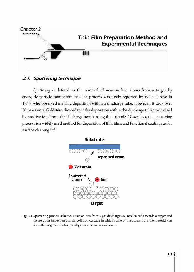
Sputteringnergetic particle853, who observ0 years until Goy positive ions frocess is a widelurface cleaning.1
g. 2.1 Sputtering prcreate upon leave the targ
hhaapptteerr 22
ing techniqu
is defined as e bombardmenved metallic deldstein showed from the dischaly used method 1,2,3
rocess scheme. Poimpact an atomic
get and subsequent
ue
the removal ont. The process eposition within
that the deposiarge bombardinfor deposition o
sitive ions from a gcollision cascade in
tly condense onto a
Thin Film E
of near surface was firstly rep
n a discharge tuition within the ng the cathode. of thin films and
gas discharge are an which some of tha substrate.
PreparatioExperimen
atoms from aported by W. Rube. However, it
discharge tube Nowadays, the
d functional coa
accelerated towardhe atoms from the
on Methodntal Techn
13
a target by R. Grove in
t took over was caused
e sputtering atings as for
s a target and e material can
d and iques

CChhaapptteerr 22
The sputtering deposition method, schematized in Fig. 2.1, is a physical vapour
deposition (PVD) process in which a bulk starting material (target) is eroded by a
particle bombardment and subsequently deposited onto a substrate. In its simplest form,
a target material is placed in a vacuum chamber filled with a particular process gas at a
reduced pressure and set on a negative potential. The negative potential accelerates the
few electrons present in the process chamber towards the grounded chamber wall. While
traversing the chamber, the electrons collide with gas molecules and generate, if the
electric field sufficient strong, electron-ion pairs. The ions from the electron-ion pairs are
accelerated towards the target (cathode) and create upon impact with the target surface
an atomic collision cascade in which some of the target material can be ejected from the
target and subsequently condense onto the surrounding surfaces.
If the electrons were only generating new charged species in the discharge, the
process would quickly extinguish since the generation of electron-ion pairs would take
place closer and closer to the chamber wall and cease when eventually the last electron is
collected at the chamber wall. However, while the ions are not able to create electron-ion
pairs to the same extent as the electrons, upon impact with the target surface they create
secondary emitted electrons which again are accelerated towards the chamber wall and
ionize as well the gas molecules. If the number of secondary emitted electrons per
incident ion times by the number of ions created in the discharge is greater or equal to
one, the discharge becomes self-sustained. The described cathodic sputtering process is
also called DC sputtering.
A disadvantage of the above described diode sputtering is the relatively low degree
of ionization of the process gas. To increase the ionization and thereby the deposition
rate, a magnetic field is commonly used to confine electrons in the discharge near the
target surface and hence increase their ionization efficiency. This method, widely known
as magnetron sputtering can, apart from increasing the deposition rate, also sustain a
discharge at a lower pressure compared to non-magnetron sputtering. A low process
pressure is usually desirable since the sputtered particles have a long mean free path in a
low pressure discharge and can therefore retain some of the kinetic energy as they
traverse the process chamber. The excess energy increases the surface diffusion of the

Thin Film preparation Method and Experimental Techniques
15
absorbed particles at the substrate surface which improved and in many cases promoted
crystal growth and the quality of the deposited film. Typical working pressures of the
sputtering process are in the 10-3-10-2 mbar range.2,4
A significant drawback of DC sputtering is that the target must consist of a
conducting material in order to avoid charging and therefore, materials of high resistivity
cannot be DC sputtered. The reason is that if an isolating target material is set on a
negative potential, the ion bombardment quickly charges up the surface of the target,
eventually resulting in an electrical breakdown in the form of arcing. However, arcing can
be avoided by using a radio frequency (RF) or pulsed DC bias.
RF sputtering is similar to DC sputtering except for the fact that alternating current
discharges are sustained instead of DC discharges. In RF sputtering, the target self-biases
to a negative potential, sputtering atoms by the positive ion bombardment. The electrons
are more mobile than the ions and hence follow the periodic changes in the AC electric
field much effectively. When the AC electrical signal is applied at the target, initially a
large electron current is drawn followed by a small positive ion current making the net
current flow different from zero over the complete period of one cycle. Net current flow
cannot be different from zero as charge cannot be transferred through a capacitor and
hence at the operating point of this cycle, the target self-biases to a negative potential –
where no net current flows. A combination of capacitors and inductors is used to form an
impedance matching network which maximizes the power delivery by forming an
effective coupling of the RF power supply and the target. The impedances of materials
with high resistivity that cannot be DC sputtered drop with increasing frequency and so,
high frequencies pass current through dielectric targets. RF frequencies that can be
employed range from 5 to 30 MHz. But the Federal Communications Commission has
reserved a frequency of 13.56 MHz for the plasma processing techniques and so is the
most widely used.2,5
The sputtering process is typically quantified by the total sputtering yield (S),
defined as the statistical mean number of sputtered particles per incident particle. S
depends on several factors related to the incident ion and target material. These factors
include ion mass, ion energy, ion angle of incidence, atomic mass of target atoms, target
CChhaapptteerr 22
atomic structure (crystal orientation/lattice system and whether target is polycrystalline,
amorphous, or comprised of a single crystal), target surface binding energy, and target
texture. Sputtering yield tends to increase with increasing incident ion mass. At incident
ion energies below the threshold energy, Eth, sputtering will not occur. Above Eth,
sputtering yield generally increases with the incident ion energy. S also enhances with
increasing target atomic masses, roughly correlated to the target atom’s location on the
periodic table. As well, S increases with the angle of incidence, from normal incidence (β
= 0°) until approximately β = 60° (30º from glancing), reaching a value of zero at β = 90°.
As the angle of incidence increases, more of the ion’s energy gets deposited closer to the
surface, until the ion is at near glancing incidence when the ion begins to be increasingly
repulsed by the target surface atoms. Single crystal targets “tunnel” the collision cascade
(due to the repeating crystal lattices) creating “spot pattern” distributions while
amorphous and polycrystalline targets behave in a more isotropic manner. Microscopic
surface features and texturing create localized changes in the angle of incidence from the
bulk of the surface, changing the local yield. These features may “shadow” other areas of
the surface (especially at oblique incidences) thus creating localized areas of reduced
sputtering. Target materials with higher surface binding energies allow fewer atoms to be
sputtered, thus lowering S.5
Thin film deposition of compounds can be performed by using a reactive working
gas, what is called reactive sputtering. This is, however, a more complex process exhibiting
a nonlinear behavior with respect to the main process parameters, such as the partial
pressure of the reactive gas, the discharge power etc. Moreover, compound is not only
formed on the substrate but also on the target surface (target poisoning) and if the
targets enter the so called compound mode, in which a compound layer is fully formed
on the surface of the target, the deposition rate substantially decreases since the process
efficiency is generally lower for the compound than for the elemental material.

Thin Film preparation Method and Experimental Techniques
17
2.1.1. Experimental equipment
All the samples studied during this work have been prepared at the sputtering
laboratory at the ICMM. The specific equipment used for the thin film sputtering
deposition is shown in Fig. 2.2. It consists of a PLS 500 Pfeiffer high vacuum system,
equipped with a TMH 520 turbomolecular pump, what allows a base pressure of about
10-7 mbar. A throttle valve between the vacuum chamber and the turbomolecular pump
enables to lessen pumping rate. A PKR 251 Pirani-Penning combined sensor (103-10-9
mbar range) from Balzers Instruments is place at the deposition chamber for the pressure
measurement.
A number of three Thin Film Consulting Gmbh planar magnetrons (2” diameter)
are placed inside the experimental chamber, what allows the deposit of diverse materials.
They can be operated by both PFG 1500-DC or PFG 300-RF power supplies (from
Hüttinger Gmbh. Electronics) for conductive or high resistive materials, respectively. A
matchbox operates coupled to the RF power supply at a frequency of 13.56 MHz. All the
magnetrons have a water cooling system. Circular targets from the corresponding
material (2” diameter and about 3 mm thickness) are mechanically clamped to the water-
cooled electrodes.
Different gasses can be introduced inside the chamber by means of UFC 1200A
mass flow controllers (MFCs) from UNIT Instruments. The purity of the gases, N2, O2,
Ar, N2/H2 and Ar/H2, is 99.999%. The different MFCs allow us to set the desired
atmosphere during growth.
An additional small load-lock chamber is placed at the left side of the deposition
chamber (see Fig. 2.2) in order to introduce the sample-holder and take it out without
opening the main chamber. This secondary chamber, connected to the main chamber by
a guillotine valve, is equipped with a mechanical pump, an IMR 260 Pirari sensor (from
Balzers Instruments) and with a sample transfer bar.

CChhaapptteerr 22
Fig. 2.2 (a) Sputtering experimental equipment from the sputtering laboratory at the ICMM used for the thin film deposition. (b) Inside of the main chamber, where the magnetrons and the rotatory disk (with the sample-holder inserted) can be observed. (c) Example of the sputtering process inside the main chamber.
The sample-holder, which is about 2” size, is introduced into the main chamber
through the transfer bar and insert into a rotary disk placed at a distance of about 10 cm
above the magnetron surfaces. The inside of the main chamber is shown in Fig. 2.2(b),
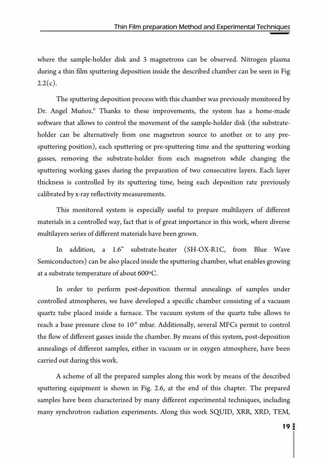
Thin Film preparation Method and Experimental Techniques
19
where the sample-holder disk and 3 magnetrons can be observed. Nitrogen plasma
during a thin film sputtering deposition inside the described chamber can be seen in Fig
2.2(c).
The sputtering deposition process with this chamber was previously monitored by
Dr. Angel Muñoz.6 Thanks to these improvements, the system has a home-made
software that allows to control the movement of the sample-holder disk (the substrate-
holder can be alternatively from one magnetron source to another or to any pre-
sputtering position), each sputtering or pre-sputtering time and the sputtering working
gasses, removing the substrate-holder from each magnetron while changing the
sputtering working gases during the preparation of two consecutive layers. Each layer
thickness is controlled by its sputtering time, being each deposition rate previously
calibrated by x-ray reflectivity measurements.
This monitored system is especially useful to prepare multilayers of different
materials in a controlled way, fact that is of great importance in this work, where diverse
multilayers series of different materials have been grown.
In addition, a 1.6” substrate-heater (SH-OX-R1C, from Blue Wave
Semiconductors) can be also placed inside the sputtering chamber, what enables growing
at a substrate temperature of about 600ºC.
In order to perform post-deposition thermal annealings of samples under
controlled atmospheres, we have developed a specific chamber consisting of a vacuum
quartz tube placed inside a furnace. The vacuum system of the quartz tube allows to
reach a base pressure close to 10-6 mbar. Additionally, several MFCs permit to control
the flow of different gasses inside the chamber. By means of this system, post-deposition
annealings of different samples, either in vacuum or in oxygen atmosphere, have been
carried out during this work.
A scheme of all the prepared samples along this work by means of the described
sputtering equipment is shown in Fig. 2.6, at the end of this chapter. The prepared
samples have been characterized by many different experimental techniques, including
many synchrotron radiation experiments. Along this work SQUID, XRR, XRD, TEM,
CChhaapptteerr 22
RBS, NRA, XPS, XANES, EXAFS, XMCD, UV-Vis Absorption and GISAXS have been
used for the thin film characterizations. In this chapter, a brief overview of several
selected techniques is given. An outlook of the experimental procedures is given in the
last part (Fig 2.7).
2.2. SQUID magnetometry
The magnetic characterization of samples was performed in a SQUID
(Superconducting Quantum Interference Device) magnetometer (MPMS-5T from
Quantum Design) at the ICMM facilities, in collaboration with Dr. Mar García
Hernández. In some cases, a SQUID (MPMS-7T from Quantum Design) was employed
for the magnetic measurements.
The SQUID is the most sensitive device available for measuring magnetic fields.
The SQUID in the MPMS system does not detect the magnetic field from the sample
directly. The measurement is performed in the MPMS instrument by moving the sample
through the superconducting detection coils, which are located at the center of the
superconducting magnet outside the sample chamber.7,8 The detection coils are
connected to the SQUID with superconducting wires, allowing the current from the
detection coils to inductively couple to the SQUID sensor. As the sample moves through
the detection coils, the magnetic moment of the sample induces an electric current in the
detection coils. The detection coils, the connecting wires and the SQUID input coil form
a closed superconducting loop. Any change in the magnetic flux in the detection coils
produces a change in the persistent current in the detection circuit, proportional to the
change in magnetic flux. Since the SQUID operates as highly linear current-to-voltage
convertor, the variations in the current in the detection coils produce corresponding
variations in the SQUID output voltage which are proportional to the magnetic moment
of the sample. In a fully calibrated system, measurements of the voltage variation as the
sample is moved through the detection coils provide a highly accurate measurement of
the sample magnetic moment. The system can be accurately calibrated using a small
piece of material having a known mass and magnetic susceptibility.

Thin Film preparation Method and Experimental Techniques
21
The Quantum Design MPMS-5T instrument with a superconducting magnet can
be operated using fields up to 5 Tesla (the MPMS-7T model up to 7 Tesla) and
measurements can be performed at temperatures ranging from 2 to 400 K. The system
makes use of a second order derivative coil configuration to eliminate effects of stray
fields. The sample chamber has low helium gas pressure, which provides thermal contact
with a flow of gas outside the sample chamber pipe that is used to change and stabilize
the temperature. Over 4.5 K flow impedance and a gas heater take care of the
temperature control. The temperature is homogenized around the sample space by
copper wires.
For the temperature dependence of magnetization, M(T), two kinds of
measurements were done. In the zero field cooling measurement (ZFC) the sample was
cooled down to 5 K in the absence of a magnetic field and a constant magnetic field was
applied during the warm up scan (usually H = 1 kOe). In the field cooling (FC)
measurements, the sample was cooled down to 5 K in the presence of the same constant
magnetic field and then, a warm up scan was performed in the same magnetic field.
Nonetheless, for the samples studied here, no appreciable differences were found
between the ZFC and FC curves. The M vs. T curves shown here correspond generally to
the FC ones.
For the hysteretic loop, M (H) measurements, the samples were subjected to a
magnetic field cycling between +5 Tesla and -5 Tesla and magnetization was measured at
a particular temperature (typically at 5 and 300 K).
2.3. X-Ray Diffraction (XRD)
X-ray diffraction (XRD) measurements have been performed in several Bruker D8
X-ray diffractometers from the ICMM diffraction service, by using the Kα radiation line
of Cu, in order to obtain information about the structure and texture of the films. The
prepared films are usually grown with textured grains. The grain size of the films in the
out-of-plane direction has been obtained by measuring the full width at half maximal

CChhaapptteerr 22
(FWHM) intensity of the Bragg diffraction peak and using the Scherrer formula (Eq.
2.1)
. (2.1)
where l is the crystallite size, λ is the wavelength of the x-radiation used, B is the peak
width (in radians) due to particle size effect, and θ is the Bragg angle.
For selected samples, additional x-ray diffraction experiments have been carried
out in a six-circle diffractometer especially designed for thin film characterization, using λ
= 0.8857 Å, at SpLine, BM25B (Spanish CRG beamline) of the European Synchrotron
Radiation Facility (ESRF), in Grenoble. In this case, apart from the usual θ-2θ
diffractograms, grazing incidence (ω = 0.75º) experiments were performed in order to
enhance the thin film signal and to avoid the strong peaks from the substrate.
2.4. X-Ray Reflectivity (XRR)
Additionally to the standard XRD characterization, X-ray reflectivity (XRR)
measurements can be done by using well focused, monochromatic x-rays. XRR curves are
possible due to the contrast in electronic density between film and air and between film
and substrate (and also between layers in the case of multilayers).9 In the hard x-ray
region the refractive index n of the materials is smaller than unity. Considering the Snell
equation, since the refractive index inside the material is now smaller than the one of air
(nair = 1), there will be an angle under which the x-rays are totally reflected. This angle is
called the critical angle (θ and it is dependent on the electronic density as:
θ (2.2)
⁄ is the classical electron radius, is wave vector and is the electronic
density.
Above the critical angle, due to the interference between the x-ray beams scattered from
the different interfaces it is possible to record a scan consisting of so-called thickness or

Thin Film preparation Method and Experimental Techniques
23
Kiessig fringes, i.e., intensity maxima corresponding to constructive interference and
minima due to destructive interference. The position of these fringes is directly related to
the thickness of the layers (d), which is in fact the Bragg equation but modified by the
influence of refraction.
2 θ θ (2.3)
where m is an integer.
Since, in most cases, the incident angle θ is sufficiently small, Eq (2.3) has the
form:
θ θ (2.4)
This relation shows a simple method to determine the layer thickness from the
measured reflectivity curve. Just by plotting the square of the angular positions of the
intensity maxima versus the squares of the Kiessig fringe order. In the validity range of Eq.
(2.4) it gives a straight line with the layer thickness d as slope.
Similarly to the case of a single layer, the modified Bragg law for the x-ray
reflectivity of a periodic multilayer containing N periods, each consisting of a layer A with
thickness tA and a layer B with thickness tB ; the multilayer period is D = tA + tB, can be
written as:
2 θ θ (2.5)
where m is an integer.
For incident angle θ sufficiently small, the equation can be simplified
θ θ (2.6)
CChhaapptteerr 22
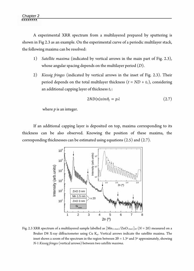
A experimental XRR spectrum from a multilayered prepared by sputtering is
shown in Fig 2.3 as an example. On the experimental curve of a periodic multilayer stack,
the following maxima can be resolved:
1) Satellite maxima (indicated by vertical arrows in the main part of Fig. 2.3),
whose angular spacing depends on the multilayer period (D).
2) Kiessig fringes (indicated by vertical arrows in the inset of Fig. 2.3). Their
period depends on the total multilayer thickness (t = ND + tC), considering
an additional capping layer of thickness tC:
2 θ λ (2.7)
where p is an integer.
If an additional capping layer is deposited on top, maxima corresponding to its
thickness can be also observed. Knowing the position of these maxima, the
corresponding thicknesses can be estimated using equations (2.5) and (2.7).
1 2 3 4 5 6 7 8
101
102
103
104
105
106
1.6 2.0 2.4 2.8
103
104
105
Inte
nsity
(arb
.uni
ts)
2θ (º)
Sisubst
Mn 1.5 nm
ZnO 3 nm
ZnO 3 nm
x 20
Inte
nsity
(arb
.uni
ts)
2θ (º)
1
2 3
11
4 57 8 9 10
19
1213
1817
141516
6
Fig. 2.3 XRR spectrum of a multilayered sample labelled as [Mn(1.5nm)/ZnO(3nm)]20 (N = 20) measured on a
Bruker D8 X-ray diffractometer using Cu Kα. Vertical arrows indicate the satellite maxima. The inset shows a zoom of the spectrum in the region between 2θ = 1.3º and 3º approximately, showing N-1 Kiessig fringes (vertical arrows) between two satellite maxima.
Thin Film preparation Method and Experimental Techniques
25
More sophisticated methods of simulating the reflectivity curves give more precise
thickness values as well as information about the inter-layer roughness. For instance,
XRR measurements of Mn/ZnO multilayers and their simulation by using the Xreal
software developed by Dr. N. Telling can be found in section 3.4.
2.5. Rutherford Backscattering Spectroscopy (RBS)
Rutherford Backscattering Spectroscopy (RBS) is a quantitative elemental-
analysis technique based on collisions between atomic nuclei (billiard-ball physics). RBS
uses a monoenergetic beam of high energy ions (typically 2-3 MeV He2+) to probe a thin
film sample and detects those incident ions which are scattered back from sample nuclei.
From the energy spectrum of the backscattered particles, elemental concentration and
their depth profiles can be calculated. This technique is nondestructive since it does not
sputter atoms from the surface.2
Each atom, when collided with an incident ion of known energy, will absorb a
discrete amount of the energy from the incident ion (momentum transfer).
Consequently, the incident ion backscatters at a lower energy that can be characterized
by Rutherford backscattering to determine the elemental composition. This technique is
very useful for measurements of low atomic number elements. Heavy elements withdraw
little energy, so they are more difficult to resolve from each other, although the sensitivity
for them is much higher since the backscatter cross-section increases as atomic number
squared. Also, the RBS signal for atoms lighter than the substrate rides on the substrate
background while heavier atoms are displayed by themselves.
The thickness of the film can be determined by the difference in backscattered ion
energy. An ion that collides with an atom at the thin film surface will backscatter the ion
with a different energy than when it collides with an atom deeper in the sample. In the
latter case, the He ion will lose energy from the nucleus collision but also from the
electron valence atoms from the sample when traveling into and out the sample before
and after the scattering. Thus, the thicker the film, the broader in energy becomes the
back-scattered peak that is evenly distributed through it, and variation in the peak height

CChhaapptteerr 22
with backscattering energy can be used to calculate depth profile with a resolution of
about 10 nm.
Most of the RBS experiments described in this work were carried out at the
Centro Nacional de Aceleradores (Sevilla, Spain) in collaboration with Dr. Javier García
López in order to determine precisely the atomic composition of the samples. The
experiments were done in a 3 MV Tandem accelerator, using a 2 MeV H2+ beam, with
beam diameter ∼ 1 mm and scattering angle of 165º.
Data analysis was usually performed through SIMNRA software,10 which is up to
now the most popular and refined one.
2.6. X-Ray Absorption Spectroscopy (XAS)
X-ray Absorption Spectroscopy (XAS) using synchrotron radiation is a well-
established technique providing information on the electronic, structural and magnetic
properties of matter. In XAS, a photon is absorbed by an atom, giving rise to the
transition of an electron from a core state to an empty state above the Fermi level. The
absorption cross-section depends on the energy and on the measured element. To excite
an electron in a given core level, the photon energy has to be equal or higher than the
energy of this core level. In XAS experiments, the photon energy is scanned from below
to above this core-level energy. The energies of the absorption edges therefore
correspond to the core-level energies, which are characteristic for each element, making
x-ray absorption an element-sensitive technique. The L3,2-edges are related to a 2p core
level while the K-edge is related to a 1s core-level binding energy.
In general, two regions can be discerned in XAS: the near-edge region or XANES
(X-ray Absorption Near-Edge Structure), which extends to an energy of the order of 50
eV above the edge and EXAFS (Extended X-ray Absorption Fine Structure), which is the
oscillatory structure in the absorption coefficient whose amplitude is typically a few
percent or less of the total absorption, and which extends over hundred of electron volts
beyond the x-ray absorption edge. The spectral shape in the XANES region is
determined by electron correlation and density of states (or multiple scattering) effects

Thin Film preparation Method and Experimental Techniques
27
and gives mainly information about the electronic properties of the absorbing atom. The
EXAFS region is dominated by single scattering events of the outgoing electron on the
neighbouring atoms, giving information about the local atomic structure around the
absorbing site. For further information about XAS spectroscopy, we refer the reader to
Ref. 11 and 12.
2.6.1. XAS experiments at the Mn and Zn K-edges
The absorptions at the K-edges are transitions from the core 1s level to the empty
4p states. In order to let the incident beam penetrate into the core levels of the atoms,
high energy x-rays must be used. Synchrotron radiation is practically the unique source
capable of producing x-rays of such high intensity. This type of source produces x-ray
radiation of the order of 105 to 106 times of the intensity of a conventional source and is
continuously tunable. XAS experiments were carried out at the European Synchrotron
Radiation Facility (ESRF), in Grenoble, with storage ring energy of 6 GeV and an
average current of 200 mA. Details of the XAS experiment carried out at the ESRF during
this disertation are the following.
Several Mn K-edge experiments were performed at different beamlines: BM26A
(Fluorescence detection), BM8 (Total Electron Yield, TEY) and, especially, at SpLine,
BM25A (Spanish CRG beamline), where Mn and Zn K-edge were measured using
fluorescence detection.
A Si(111) double crystal pseudo channel-cut monochromator was used for energy
selection and sample was vertically shifted while the spectrum was collected. Incident
beam was typically monitored by means of an ion chamber filled with a mixture of N2 and
He, and the Mn and Zn Kα lines fluorescence yield was collected using a Si(Li) detector,
from e2v Scientific Instruments. The monochromator was detuned up to 70% for those
energy ranges to reject components of higher harmonics. Several spectra were collected
in order to improve statistics and to have a good signal to noise ratio. Fluorescence
spectra were obtained at room temperature under geometry where the angle between
the detector and the incoming beam was 90º and the corresponding between the sample

CChhaapptteerr 22
and the incoming beam was 45º. The energy calibration was monitored using Mn and Zn
foils. In some cases, measurements of the Zn K-edge were achieved by adding a Cr filter
(6 μm foil) between the sample and detector and a smaller angle collection by increasing
the sample-detector distance, in order to avoid detector saturation.
2.6.1.1. X-Ray Absorption Near-Edge Structure (XANES)
The Mn oxidation state in the prepared samples has been investigated by XANES.
The edge position depends on the oxidation state of the absorber, being shifted to higher
energies when increasing its formal valence. This can be observed in Fig. 2.4, which
shows the XANES spectra at the Mn K-edge of metallic Mn and different oxides, where
distinct differences in the form and in the position of the edges can be noticed.
From a simplified point of view, the sensitivity to valence is due to the core-hole
interaction with the electron localized or quasi-localized on the excited atom. If one shifts
from a valence, for example Mn2+ to Mn3+, the filling of the 3d elements changes and
consequently its nucleus is less well screened, resulting in an increased binding energy of
the deepest core levels and therefore shifting the edge to higher energies.13
6530 6540 6550 6560 65700.0
0.4
0.8
1.2
6536 6540 6544 65480
1
2
3
4
Nor
mal
ized
Inst
ensi
ty
Energy (eV)
Mn K-edge
Mn
vale
nce
Energy (eV)
Metallic Mn
MnO
MnO2
MnOOH
Fig. 2.4 XANES spectrum of Mn0, Mn2+ (MnO), Mn3+ (MnOOH) and Mn4+ (MnO2) references.14 The inset
shows the linear relationship between threshold energy and oxidation state.
The form of the absorption edges reflects the empty electronic density of states
and is strongly dependent, for example, on the type of atomic coordination, like linear,

Thin Film preparation Method and Experimental Techniques
29
tetrahedral (Td) or octahedral (Oh) coordination. XANES computational methods allow
to obtain important information on the sample structure. XANES calculations of the Mn
K-edge XANES spectra have been carried out in collaboration with Dr. Jesús Chaboy
from the Instituto de Ciencia de Materiales de Aragón, using the multiple-scattering code
CONTINUUM15 based on the one-electron full-multiple-scattering theory16,17,
obtaining significant information on the Mn/Si3N4 studied samples. Details of the
simulations are described in section 6.8.2.
2.6.1.2. Extended X-Ray Absorption Fine Structure (EXAFS)
The origin of the EXAFS signal is related to an interference effect that evolves
scattering of the outgoing photoelectron from the neighboring atoms. From a qualitative
viewpoint, the probability that an x-ray photon will be absorbed by a core electron
depends on both the initial and the final states of the electron. The initial state is the
localized core level corresponding to the absorption edge. The final state is that of the
ejected photoelectron which can be represented as an outgoing spherical wave
originating from the x-ray absorbing atom. If the absorbing atom has a neighboring atom,
the outgoing photoelectron wave will be backscattered by the neighboring atom, thereby
producing an incoming electron wave. The final state is then the sum of the outgoing and
all the incoming waves, one from each neighboring atom. It is the interference between
the outgoing and the incoming waves that gives rise to the sinusoidal variation of μ vs E
known as EXAFS.
By EXAFS analysis at the Mn absorption K-edge we can obtain precise
information of the local environment (neighbours, coordination and bond length)
around Mn, which results of great important in the field of DMS. The technique is not
restricted by long-range order and is element-sensitive, being of great importance for
noncrystalline solids and highly diluted materials.
The analysis of the EXAFS signal was performed in the following way. EXAFS
oscillations were obtained after removing the atomic background by a cubic spline
polynomial fitting, and EXAFS signal (χ(k)) was found by normalizing the magnitude of

CChhaapptteerr 22
the oscillations to the edge jump. The resulting data were transformed into a function of
the photoelectron wavenumber, k.
The pseudo Radial Distribution Function around the absorber atoms was
calculated by Fourier transforming the kn-weighted EXAFS signal (kn·χ(k)) multiplied
previously by a Hanning window (where typically n = 1,2 or 3). To obtain neighbours
distances and coordination numbers, the back Fourier transform of first and second
peaks was fitted to the well-known expression:11
∑ Φ+×= −−
jjjj
kRk
j
j kkRkfeekRN
Sk jj ))(2sin()()( ))(/2()2(2
20
22 λσχ (2.8)
Eq. (2.8) describes the EXAFS oscillations for a Gaussian distribution of Nj atoms at
mean distances Rj around the absorbing atom, considering single scattering and plane-wave
approximation. S02 is an intrinsic loss factor, Nj is the average coordination number for the
Gaussian distribution of distances centered at the Rj value, σj is the Debye-Waller factor, and
φj(k) = 2δ(k)+ϕj(k) is the phase shift, being δ(k) and ϕj(k) the central and backscattering
atom phase shifts, respectively. fj(k) is the magnitude of the backscattering amplitude of the
jth-neighbour atom, and λ is the mean free path of the photoelectron traveling from the
absorbing atom to the backscatterer in the jth- shell and the life time of the core hole.
For all the samples, FTs were obtained over the same k2-weighted interval (over a
wave vector range from approximately 2 to 10 Å-1) by using amplitude and phase
backscattering functions calculated by the FEFF6 code,18 where the scattering potentials
are calculated in a standard way for atomic-charge densities within the muffin-tin (MT)
approximation. The potential also includes the Hedin-Lundqvist self-energy with the
Quinn correction to account for low-energy electron-hole losses. The conventional non-
overlapping MT spheres approximation is used, since, for the EXAFS regime, the
electron-atom scattering is dominated by the nearly spherical potential inside the muffin-
tin and has low effect at these energies.19

Thin Film preparation Method and Experimental Techniques
31
2.6.2. XAS at the Mn L3,2−edge
A 2p electron has dipole-allowed transitions to s- and d-like final states. Due to the
large wavefunction overlap, the 3d channel is much stronger than the other channels, and
the 2p absorption is determined by the transition probability 2p63dn → 2p5dn+1. The L3,2
absorption spectrum, which consists of a 2p3/2 (L3) and 2p1/2 (L2) structure, is therefore
dominated by dipole transitions from the core 2p level to the empty 3d states, and
because of the large Coulomb interaction between these two levels, it depends on the
local electronic structure. Thus, analysis of the L3,2 absorption structure can provide
information about the oxidation state and the symmetry of the 3d transition metal ions.20
There are some important L3,2 spectral features to be mentioned:
Ions with the same number of 3d electrons give similar L3,2 spectra, except for the
size of the 2p spin-orbit separation and the absolute energy. However, the spectra of
different dn configurations are quite different and this can be used to identify the valence
of an element. The energy separation between two oxidation states dn and dn+1 of a
particular element is equal to Q-U, where Q and U are the 2p → 3d and the 3d → 3d
Coulomb interactions, respectively. Since Q is larger than U, the highest oxidation state
(dn) has the highest energy.
The crystal field interaction mixes states with different L values in the ground state
LS term, allowing transitions to other final states with the same spin. This gives rise to a
broadening of the peaks and a gradual appearance of new peaks with increasing crystal
field interactions. Abrupt changes in the spectra are indicative of spin transitions.
Details of the Mn L3,2-edge experiments are the following. Mn L3,2-edge XAS
measurements were done at beamline 5U.1 of the Synchrotron Radiation Source (SRS)
at Daresbury Laboratory, in UK, in collaboration with Prof. G. Van der Laan and Dr. N.
Telling. Spectra were collected between 630 and 670 eV in TEY mode.
Along this dissertation, information of the Mn ground state, Mn symmetry and
crystal field has been obtained by comparison of the sample spectra with theoretical
calculations for different manganese electronic configurations (section 6.8.3).
CChhaapptteerr 22
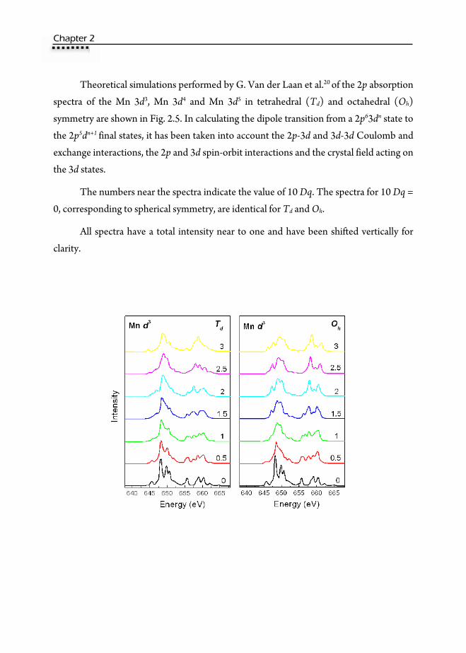
Theoretical simulations performed by G. Van der Laan et al.20 of the 2p absorption
spectra of the Mn 3d3, Mn 3d4 and Mn 3d5 in tetrahedral (Td) and octahedral (Oh)
symmetry are shown in Fig. 2.5. In calculating the dipole transition from a 2p63dn state to
the 2p5dn+1 final states, it has been taken into account the 2p-3d and 3d-3d Coulomb and
exchange interactions, the 2p and 3d spin-orbit interactions and the crystal field acting on
the 3d states.
The numbers near the spectra indicate the value of 10 Dq. The spectra for 10 Dq =
0, corresponding to spherical symmetry, are identical for Td and Oh.
All spectra have a total intensity near to one and have been shifted vertically for
clarity.

Thin Film preparation Method and Experimental Techniques
33
Fig. 2.5 Theoretical simulations performed by G. Van der Laan et al. 20 of the 2p absorption spectra of the Mn 3d3, Mn 3d4 and Mn 3d5 in tetrahedral (Td) and octahedral (Oh) symmetry. The numbers close to the spectra indicate the value of 10 Dq. All spectra have a total intensity near to one and have been vertically shifted for clearness.

CChhaapptteerr 22
2.6.3. X-ray Magnetic Circular Dichroism (XMCD)
Dichroism with circularly polarized x-rays (X-ray Magnetic Circular Dichroism or
XMCD) has become a powerful tool for the study of magnetic materials, capable to
provide element specific information about spin and orbital magnetic moments.
With x-rays, in some cases, there is a difference between the absorption of left and
right circularly polarized light (circular dichroism) or for different orientations of the
polarization vector of linearly polarized light (linear dichroism). Magnetic dichroism
occurs when the spherical symmetry of the free atom is broken due to a magnetic field,
having its origin in the spin-orbit interaction. On the microscopic level, circular
dichroism is given by the difference between ∆MJ = +1 and ∆MJ = -1 transitions, while
linear dichroism is related to the difference between ∆MJ = 0 and ∆MJ = ±1 transitions.13
More details about the XMCD origin of the 3d transition-metal ions are described
below.
In the spherically symmetric potential of a free ion, a small 3d spin-orbit
interaction will split the initial state LS terms into levels LSJ. These levels are (2J+1)-fold
degenerate, corresponding to the number of different eigenvalues MJ = -J, -J+1,..., J.
The electrons are coupled to those of neighbouring atoms by exchange
interactions (direct-exchange and superexchange in the case of non-metallic systems)
which are usually between 0.005 and 0.1 eV. The interatomic exchange interaction in the
3d metal compounds can be treated as a magnetic field acting on the spin S. This
exchange field lifts the degeneracy, making the energy of the MJ sublevels equal to –
gμBHMJ, where only the level with MJ = -J is populated at T = 0 K. The factor g depends
on the values of L, S and J. If the exchange interaction is of the same order of magnitude
as the spin-orbit interaction, the different J levels within the term are strongly mixed. The
energy of the final-state levels J’ is determined by the electrostatic interactions in the
2p5dn+1 configuration and the large core-hole spin-orbit interactions, which splits the
spectrum into a 2p3/2 and 2p1/2 parts.
Magnetic dichroism is induced by the optical selection rules. For an initial state
Thin Film preparation Method and Experimental Techniques
35
level J, the dipole selection rule ∆J = +1, 0, -1 permits only transitions to final-state levels
J’= J+1, J and J-1. Excitation with left-circularly polarized radiation (∆MJ = -1) is then
only allowed to J’= J+1 levels (the only levels which contain an MJ’=-MJ +1 sublevel).
The levels with different total angular momentum J’ in the final-state configuration
have a different energy distribution due to the electronic interactions between the 2p
core-hole and the 3d valence electrons, and the 2p core-hole spin-orbit interaction.
Therefore, the spectra for left- and right-circularly polarized radiation will be different.21
If the absorption cross-sections for left and right circular polarizations are
respectively, σ+ and σ-, the asymmetry (R) measured by the XMCD is:
(2.9)
The conditions necessary for a non-zero value for R are: spin-orbit coupling in the
final state of the excitation, macroscopic magnetization (ferro- o ferrimagnetic samples)
and a circularly polarized beam.
The degree of circular polarization of the X-ray photons is about 1% for K-edge
and larger for L2 and L3-edges. The difference is due to the presence of a strong spin-orbit
coupling in the initial state of the L3,2 edges (2p bands) which is not present in the initial
state of the K edge (1s band).
Details of the Mn L3,2-edge XMCD experiments are the following. XMCD
measurements were done on beamline 5U.1 of the Synchrotron Radiation Source at
Daresbury Laboratory. Spectra were collected in TEY mode reversing the applied
magnetic field of ± 0.6 T perpendicular to the surface at each data point for fixed photon
helicity. Reversal of the XMCD signal was confirmed by switching between left and right
circular polarization. Comparison between the obtained spectra with dn calculations was
done. XMCD measurements are included in section 6.8.4.

CChhaapptteerr 22
Fig. 2.6 The families of samples that have been studied in this dissertation.
Post‐growth annealing (Vacuum;O2); t = 1.5, 0.7 nm TS = 25°C, 300°C, 600°C; t = 6 nm
Part II: Mn‐Si3N4 system
a) [Mn(tm)/Si3N4(3nm)]n tm = 6…0.1 nm; n = 5…75
b) [Mn(0.6nm)/Si3N4(tsn)]n tsn = 6…0.7 nm; n = 43
Chapter 6 Mn/Si3N4 MLs
[Si3N4(6nm)/Au(t)]n tAu = 8…2 nm
n = 5…75
[ZnO(3nm)/Au(t)]n tAu = 8…2 nm
n = 5…75
Appendix C1 Appendix C2
Appendix C: Au NPs in Si3N4 & ZnO
Chapter 5 Mn:ZnO films
Part I: Mn‐Zn‐O system
[Mn(t)/ZnO(3nm)]n t = 6…0.1 nm
n = 5…75
Chapter 3 Mn/ZnO MLs
[MnOx(t)/ZnO(3nm)]n t = 1, 0.5 Å n = 75
Zn0.95Mn0.05O target Sputt. gas: Ar, Ar/N2, Ar/O2
TS = 25°C, 600°C O2 post‐growth annealing
Chapter 4 MnOx/ZnO MLs
Appendix A
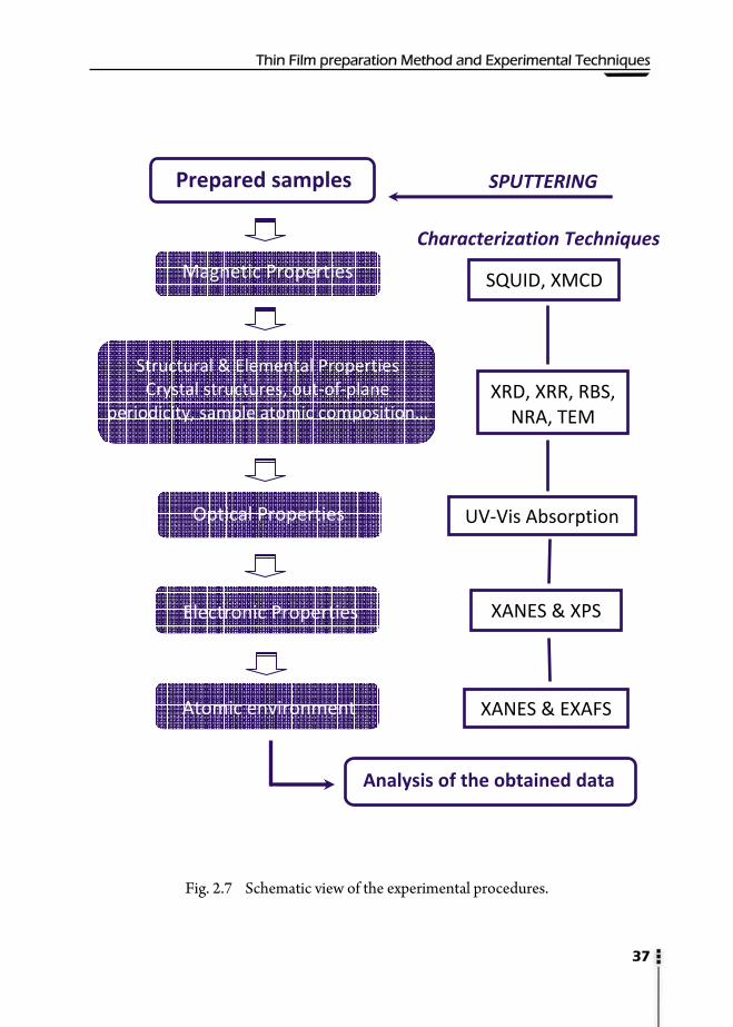
Thin Film preparation Method and Experimental Techniques
37
Fig. 2.7 Schematic view of the experimental procedures.
Analysis of the obtained data
Prepared samples
Magnetic Properties
XRD, XRR, RBS, NRA, TEM
XANES & XPS
XANES & EXAFS
Electronic Properties
Atomic environment
Optical Properties UV‐Vis Absorption
Structural & Elemental Properties Crystal structures, out‐of‐plane
periodicity, sample atomic composition…
SPUTTERING
Characterization Techniques
SQUID, XMCD

CChhaapptteerr 22
References
1 R. Parsons, “Thin Film Processes II” ( CA, USA: Academic Press Limited, 1991).
2 D. L. Smith, “Thin-Film Deposition. Principles and Practice” (McGraw-Hill, Inc. New York, 1995).
3 J. M. Albella, “Láminas delgadas y recubrimientos: preparación, propiedades y aplicaciones” (CSIC, 2003).
4 R. Daniel, Doctoral Thesis “Studies of the Reactive Sputtering Process and its Application in Electro-Acoustic Devices” (Uppsala Universitet, 2006).
5 K. A. Zoerb, Doctoral Thesis “Differential Sputtering Yields of Refractory Metals by Ion Bombardment at Normal and Oblique Incidences” (Colorado State University, 2007).
6 A. Muñoz-Martín, Appendix 2 of Doctoral Thesis “Caracterización estructural de sistemas magnéticos nanoestructurados” (ICMM-CSIC, UAM, 2002).
7 MPMS-5S Quantum Design SQUID manual.
8 A. Gupta, Doctoral Thesis “Novel Room Temperature Ferromagnetic Semiconductors”, Royal Institute of Technology, Stockholm (2004).
9 V. Holý, U. Pietsch, T. Baumbach, “High-resolution X-ray Scattering from Thin Films and Multilayers” (Springer, 1999)-
10 SIMNRA 6.04 User’s guide, http://www.ipp.mpg.de/~mam/
11 D.C. Koninsberger and R. Prins "X-Ray Absorption: Principles, Applications, Techniques of EXAFS, SEXAFS and XANES", (Wiley, New York, 1988).
12 B.K. Teo “EXAFS: Basic Principles and Data Analysis” (Springer-Verlag, Berlin Heidelberg New York Tokyo, 1986).
13 F. Hippert, E. Geissler, J. L. Hodeay, E. Lelièvre-Berna, J. R. Regnard, “Neutron and X-ray Spectroscopy” (Springer, 2006).
14 D.A. McKeown and J.E. Post, Am. Mineral. 86, 701 (2001).
15 C. R. Natoli and M. Benfatto, (unpublished).
16 P. A. Lee and J. B. Pendry, Phys. Rev. B 11, 2795 (1975).
17 C. R. Natoli and M. Benfatto, J. Phys. (Paris) Colloq. 47, C8-11 (1986).
18 S. I. Zabinsky, J. J. Rehr, Phys. Rev. B 52, 2995 (1995).

Thin Film preparation Method and Experimental Techniques
39
19 J. J. Rehr and R.C. Albers, Rev. Mod. Phys. 72, 621 (2000).
20 G. van der Laan and I. W. Kirkman, J. Phys.: Condens. Matter 4, 4189 (1992).
21 G. van der Laan and B. T. Thole, Phys. Rev. B 43, 13401 (1991).


PART I
Mn-ZnO System


41
3.1. Motivation
The special interest of the work presented in this chapter lays in the fact that the
preparation of Mn/ZnO multilayered stacks enables to study the Mn-ZnO interface and
its role in the ferromagnetism of the Mn-Zn-O system. Although the interface-related
properties have been claimed to be of great importance in the magnetic properties of this
system,1,2 to our knowledge, there has not been any previous study published dealing
with Mn/ZnO interfaces.
Conversely, multilayer structures preparation has been reported for other similar
ZnO-based materials, such as Co/ZnO thin films by sputtering,3 by ion-beam assisted
sputtering4 and CoFe/ZnO thin films prepared also by ion-beam sputtering,5 where
ferromagnetic behaviour has been observed. However, there has not been any previously
reported study on Mn/ZnO multilayers to the one described here. Only Huang et al.6
have recently reported investigations on [ZnO(20Å)/Co(1Å)]25 and
[ZnO(20Å)/Mn(1Å)]25 multilayers prepared by molecular beam epitaxy (MBE),
mainly based on the role of the lattice disorder caused by the different dopants on ZnO.
In addition to the novelty of this study, it should be noted that a comprehensive
structural characterization of the Mn/ZnO sample series has been performed combining
different laboratory and synchrotron radiation techniques. Detailed characterizations are
of great importance in this field since, in many cases, contradictory experimental results
are due to insufficient structural studies. In particular, the use of techniques such as X-ray
absorption near-edge structure (XANES) and extended X-ray absorption fine structure
(EXAFS) spectroscopies in these investigations should be underlined. These powerful
tools have previously been used to show that Mn substitutes Zn in the ZnO wurtzite
CChhaapptteerr 33
Mn/ZnO Multilayers
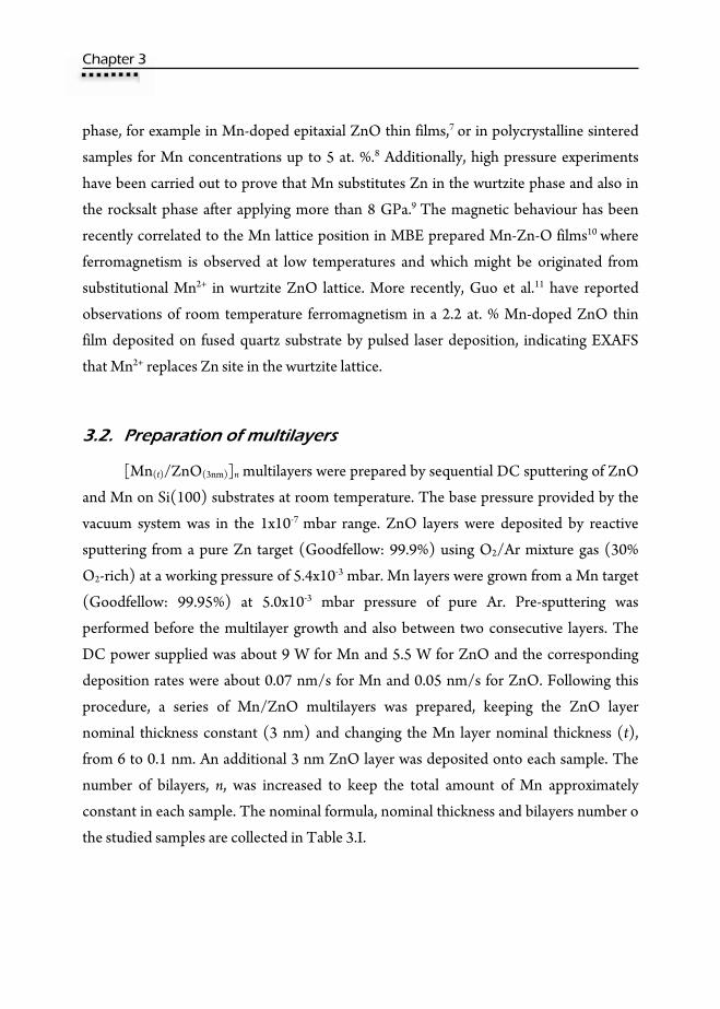
CChhaapptteerr 33
phase, for example in Mn-doped epitaxial ZnO thin films,7 or in polycrystalline sintered
samples for Mn concentrations up to 5 at. %.8 Additionally, high pressure experiments
have been carried out to prove that Mn substitutes Zn in the wurtzite phase and also in
the rocksalt phase after applying more than 8 GPa.9 The magnetic behaviour has been
recently correlated to the Mn lattice position in MBE prepared Mn-Zn-O films10 where
ferromagnetism is observed at low temperatures and which might be originated from
substitutional Mn2+ in wurtzite ZnO lattice. More recently, Guo et al.11 have reported
observations of room temperature ferromagnetism in a 2.2 at. % Mn-doped ZnO thin
film deposited on fused quartz substrate by pulsed laser deposition, indicating EXAFS
that Mn2+ replaces Zn site in the wurtzite lattice.
3.2. Preparation of multilayers
[Mn(t)/ZnO(3nm)]n multilayers were prepared by sequential DC sputtering of ZnO
and Mn on Si(100) substrates at room temperature. The base pressure provided by the
vacuum system was in the 1x10⁻⁷ mbar range. ZnO layers were deposited by reactive
sputtering from a pure Zn target (Goodfellow: 99.9%) using O2/Ar mixture gas (30%
O2-rich) at a working pressure of 5.4x10⁻³ mbar. Mn layers were grown from a Mn target
(Goodfellow: 99.95%) at 5.0x10⁻³ mbar pressure of pure Ar. Pre-sputtering was
performed before the multilayer growth and also between two consecutive layers. The
DC power supplied was about 9 W for Mn and 5.5 W for ZnO and the corresponding
deposition rates were about 0.07 nm/s for Mn and 0.05 nm/s for ZnO. Following this
procedure, a series of Mn/ZnO multilayers was prepared, keeping the ZnO layer
nominal thickness constant (3 nm) and changing the Mn layer nominal thickness (t),
from 6 to 0.1 nm. An additional 3 nm ZnO layer was deposited onto each sample. The
number of bilayers, n, was increased to keep the total amount of Mn approximately
constant in each sample. The nominal formula, nominal thickness and bilayers number o
the studied samples are collected in Table 3.I.

Mn/ZnO Multilayers
43
Table 3.I. Nominal sample series description.
Nominal sample [Mn(t)/ZnO(3nm)]n
Mn-layer nominal thickness t (nm)
Number of bilayers n
Mn total nominal thickness (nm)
Nominal sample thickness (nm)
[Mn(6nm)/ZnO(3nm)]5 6 5 30 48
[Mn(3nm)/ZnO(3nm)]10 3 10 30 63
[Mn(1.5nm)/ZnO(3nm)]20 1.5 20 30 93
[Mn(0.7nm)/ZnO(3nm)]43 0.7 43 30 162
[Mn(0.4nm)/ZnO(3nm)]75 0.4 75 30 258
[Mn(0.2nm)/ZnO(3nm)]75 0.2 75 15 243
[Mn(0.1nm)/ZnO(3nm)]75 0.1 75 7.5 236
3.3. Magnetic properties
Magnetic characterization of these samples is shown in Fig. 3.1, where
magnetization per manganese atom has been calculated taking into account the precise
amount of Mn obtained by Rutherford Backscattering Spectroscopy experiments (shown
in section 3.5). The silicon substrate diamagnetic contribution has been subtracted at the
plots.
The temperature dependence of magnetization, M(T), depicted in Fig. 3.1(a),
shows that the magnetic behaviour of the samples varies within the series, being the
ferromagnetic order favoured by increasing the Mn layer thickness (t). Ferromagnetism
over room temperature is clearly observed for the film with the thickest Mn layer (t = 6
nm). As t is reduced, the ferromagnetic component of the magnetization decreases, while
the paramagnetic one increases. Finally, samples with very thin Mn layers (t < 1.5 nm)
exhibit paramagnetic-like behaviour. The inset of Fig. 3.1(a) shows the Curie-Weiss
behaviour for the t = 0.1 nm sample, which implies a negative Curie temperature (θ ≈ -68
K), indicating that the dominant magnetic interactions between Mn atoms are
antiferromagnetic in nature, in agreement with some results previously reported in the
Mn-Zn-O system.12,13 Fig. 3.1(b) shows hysteresis loops at several temperatures of two
ferromagnetic samples. The sample with t = 6 nm exhibits about 0.05 μB per Mn atom,

CChhaapptteerr 33
being the highest saturation magnetization among the studied samples, and a coercive
field of approximately 80 Oe at 5 K. MS of about 0.05 μB/Mn corresponds to about 4 emu
per gram of Mn and to 10 emu/cm3, considering the film volume.
Fig. 3.1 (a) Magnetization curves (H = 1kOe) for several representative samples. The inset shows the inverse of magnetization vs. temperature for the t = 0.1 nm sample. Solid line corresponds to the linear fit from 100 to 350 K. (b) Hysteresis loops of the t = 6, 3 nm samples at different temperatures. The inset shows the low field region of hysteresis loop at 5 K (t = 6 nm sample).

Mn/ZnO Multilayers
45
These values are comparable to those previously reported in the literature. For
instance, MS of 1 emu/cm3 and a coercive force (HC) around 50 Oe were claimed to be
obtained at 5 K for a ZnO/MnO2 multilayer film by M. A. García et al.2 In addition, MS of
0.28 emu/g (5.6 emu/g considering the Mn amount) and HC of 78 Oe at 10 K have been
obtained by Kundaliya et al.1 for RTFM nano-sized Zn0.95Mn0.05O. Finally, a higher MS
value of 0.18 μB/Mn has been reported by S. S. Yan et al.3 for a 2 at. % Mn-doped ZnO
sample. After these comparisons, it is possible to conclude that the here prepared
ferromagnetic multilayers lay in the typical magnetization range reported for the Mn-Zn-
O system.
On the other hand, it should be remarked that the possibility of ferromagnetism
due to any extrinsic ferromagnetic impurity in these samples can be rejected. X-ray
absorption experiments performed at L-edges at beamline 5U.1 of SRS at Daresbury
Laboratory, in the UK, in collaboration with Prof. Gerrit Van der Laan and Dr. Neil
Telling, have show that there is no appreciable Fe, Co or Ni contamination in these films.
In addition, the different magnitudes of M(T) observed within the sample series also
indicate that ferromagnetism cannot be due to uncontrolled magnetic impurities from
the starting Mn target. M(T) normalized to the total number of Mn atoms (and
therefore to the possible amount of extrinsic impurity atoms) shows different
magnetization values within the sample series, being dependent of the Mn layer thickness
(t). This indicates that ferromagnetism due to uncontrolled ferromagnetic impurities,
where the magnetization would be proportional to the impurity amount, can be
discarded.
In addition, magnetic measurements were performed on several pure ZnO thin
films deposited on the same type of silicon substrates to discard any possible
ferromagnetic contribution. Magnetization vs. applied field measurement at 4.2 K for a
pristine ZnO thin film prepared by sputtering has been shown in Fig. 3.2, where no
appreciable ferromagnetic signal is observed.

CChhaapptteerr 33
-40000 -20000 0 20000 40000
-3.0x10⁻⁴
-1.5x10⁻⁴
0.0
1.5x10⁻⁴
3.0x10⁻⁴
Raw experimental data After substracting Sisubst
M (e
mu/
cm2 )
H (Oe)
Pure ZnO sputtered film
T = 4.2 K
Fig. 3.2 M-H curve from a pure ZnO film prepared by sputtering with approximately 0.4 micron thickness,
measured at 4.2 K. Raw experimental data as well as the data after subtracting the diamagnetic contribution from the silicon substrate have been included for comparison, showing that no appreciable ferromagnetic signal is obtained.
3.4. X-Ray Reflectivity (XRR)
X-ray reflectivity (XRR) measurements were carried out on a Bruker D8 X-ray
diffractometer with a Cu Kα source at the ICMM facilities. X-ray reflectivity (XRR)
sample spectra, depicted in Fig. 3.3, show multilayer periodicity in the out-of-plane
direction for all the samples, which confirms that the samples are actually formed
by layers of different electronic density.
Average thickness values of Mn and ZnO-rich layers have been obtained from
simulations of the reflectivity data (included in Fig. 3.3) performed with the Xreal
software developed by Dr. Neil Telling.14 It should be noted that these simulations make
possible higher accuracy in the layer thickness determination than performing just direct
XRR data analysis. Simulations have been done here mainly with that purpose, being
complex data fitting away from the aim of this work. That is the reason why just a short
number of parameters has been used in the calculated spectra and why these simulations
do not fully reproduce the experimental data. Some parameters from the simulations are,

Mn/ZnO Multilayers
47
for instance, silicon substrate roughness (rms), about 0.6 nm, reflected intensity
background (∼ 10-6-10-5 cps), interface roughness (∼ 0.7 nm), Mn and ZnO densities
(7.3 g/cm3 and 5.7 g/cm3, respectively) and the thickness of each layer.
Since the calculations do not completely fit the experimental data, the
comparison indicates interface roughness a bit larger in the samples as well as some
additional effects not considered here, as possible in-depth variations of the parameters.
Nonetheless, the interface roughness in the simulations (∼ 0.7 nm) indicates that, at least
for Mn thickness (t) smaller than 0.7 nm non-continuous Mn growth is expected, which points out to cluster formation for t ≤ 0.7 nm samples.
Fig. 3.3 X-ray reflectivity multilayer spectra and their simulations. From top to bottom, spectra of samples t
= 6, 3, 1.5 and 0.2 nm. All spectra have been vertically shifted for clearness.
Considering the particular case of the t = 6 nm sample, simulations by using pure
ZnO and Mn layers (simulation (a) of Fig 3.3, in blue) did not match very well the
experimental data. For this spectrum, better agreement was obtained, especially at low
angles, by considering two mixed Mn-Zn-O layers with slightly different densities (6.5
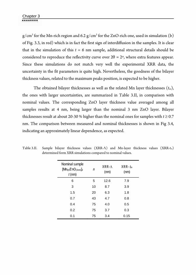
CChhaapptteerr 33
g/cm3 for the Mn-rich region and 6.2 g/cm3 for the ZnO-rich one, used in simulation (b)
of Fig. 3.3, in red) which is in fact the first sign of interdiffusion in the samples. It is clear
that in the simulation of this t = 6 nm sample, additional structural details should be
considered to reproduce the reflectivity curve over 2θ = 2º, where extra features appear.
Since these simulations do not match very well the experimental XRR data, the
uncertainty in the fit parameters is quite high. Nevertheless, the goodness of the bilayer
thickness values, related to the maximum peaks position, is expected to be higher.
The obtained bilayer thicknesses as well as the related Mn layer thicknesses (tm),
the ones with larger uncertainties, are summarized in Table 3.II, in comparison with
nominal values. The corresponding ZnO layer thickness value averaged among all
samples results at 4 nm, being larger than the nominal 3 nm ZnO layer. Bilayer
thicknesses result at about 20-30 % higher than the nominal ones for samples with t ≥ 0.7
nm. The comparison between measured and nominal thicknesses is shown in Fig 3.4,
indicating an approximately linear dependence, as expected.
Table 3.II. Sample bilayer thickness values (XRR-Λ) and Mn-layer thickness values (XRR-tm) determined form XRR simulations compared to nominal values.
Nominal sample [Mn(t)/ZnO(3nm)]n
t (nm) n
XRR-Λ (nm)
XRR- tm (nm)
6 5 12.6 7.9
3 10 8.7 3.9
1.5 20 6.3 1.8
0.7 43 4.7 0.8
0.4 75 4.0 0.5
0.2 75 3.7 0.3
0.1 75 3.4 0.15

Mn/ZnO Multilayers
49
Fig. 3.4 Comparison between the nominal bilayer thickness of samples and the experimental values
obtained by XRR measurements.
Considering the obtained Mn layer thickness values (tm), further exploration of
the ferromagnetic response of the samples has be done. In particular, it has been found
that there exists an approximately linear dependence of the saturation magnetization at
room temperature vs. tm, which is shown in Fig. 3.5. The comparison between the M-H
curves for the most ferromagnetic sample within the series (tm = 7.9 nm) and the tm = 0.15
nm one, showing just paramagnetic-like response, is included in the insets.
Fig. 3.5 Evolution of MS at RT vs. tm. The straight line corresponds to the linear fit of data. The insets show the M-H curves for the samples tm = 0.15 and 7.9 nm.

CChhaapptteerr 33
It should be noted that, for simplicity, these samples will be named by their
nominal values from now on in this chapter.
3.5. Rutherford Backscattering Spectroscopy (RBS)
RBS experiments were carried out in collaboration with Dr. Javier García López at
the Centro Nacional de Aceleradores (CNA) in Sevilla to evaluate the actual amount of
Mn in each sample as well as the film atomic composition.
Fig. 3.6 shows experimental data and simulations of some representative samples.
Fig. 3.6(a) exhibits the RBS spectra obtained with incident ions of 2 MeV and their
simulations in order to obtain the film compositions. Additionally, RBS spectra were
collected with incident ions of 8 MeV to distinguish the Mn and Zn contributions. As it
can be observed in Fig. 3.6(b), Mn and Zn contributions are separated and both integrals
can be easily evaluated. Nevertheless, for these energies, Mn and Zn cross sections are
not known and simulation cannot be performed in a similar way as for the spectra
collected at 2 MeV. However, the Mn/Zn ratio can be calculated since it is proportional
to the integral ratio of both contributions, which become well separated at 8 MeV.
Therefore, using the Mn/Zn ratio for the t = 6 nm sample obtained with 2 MeV (where
both concentrations can be obtained by simulation) the actual ratio in the whole set of
samples can be calculated. After analysis of the two used energies, the obtained film
composition is given in Table 3.III. It can be noticed that, despite considering that the
uncertainty in the oxygen amount determined by RBS (∼10-20%) is quite higher than for
heavier elements as Mn or Zn, there are considerably more oxygen atoms than zinc
atoms in these samples. The obtained atomic % of oxygen, which results roughly the
same for all the samples, suggests that the oxygen in these samples might be related to
zinc from ZnO but also to manganese.
Mn/ZnO Multilayers
51
Fig. 3.6 (a) RBS spectra taken at energy of incident ions of 2 MeV (dots) and their simulations (lines) of samples t = 6 nm, t = 3 nm, t = 1.5 nm t = 0.2 nm, from top to bottom. All spectra have been vertically shifted for clearness. (b) RBS spectra of the same samples at 8 MeV.

CChhaapptteerr 33
Table 3.III. Number of Mn atoms per Mn layer (at./cm2) and sample atomic composition (%) obtained from simulations of RBS data.
Nominal sample [Mn(t)/ZnO(3nm)]n
t (nm)
Mn atoms per Mn-layer
(1016 at./cm2)
Atomic composition (%) [Mn] [Zn] [O]
6 3.71 0.35 0.12 0.53
3 2.62 0.35 0.16 0.49
1.5 1.31 0.25 0.22 0.53
0.7 0.76 0.19 0.29 0.52
0.4 0.54 0.16 0.33 0.51
0.2 0.42 0.13 0.34 0.53
0.1 0.35 0.11 0.34 0.55
A comparison between the Mn layer thicknesses previously obtained by XRR
simulations and the calculated ones by taking into account the RBS results (where the
metallic Mn density, 8.1x10²² at./cm3 has been used) is shown in Fig. 3.7. The most
noticeable fact is that, for samples with thick enough Mn layers, XRR-determined Mn-
layer thickness is larger than the corresponding value obtained from RBS. Since XRR is a
thickness direct measurement, this apparent discrepancy can be explained in terms of the
considered Mn density. This means that in the thickness calculation from RBS data, the
used metallic Mn density is, in fact, higher than the actual one. This fact directly points
towards the existence of oxidized Mn layers in the samples. The relation between the
straight-line slopes corresponding to both techniques can be used to estimate the average
Mn layer density in the samples. The obtained slope, 4.4x10²² at./cm3, is clearly smaller
than the value corresponding to metallic Mn (8.1x10²² at./cm3). A comparison with
some manganese oxides like MnO (4.6x10²² at./cm3), Mn2O3 (1.9x10²² at./cm3) or
MnO2 (3.5x10²² at./cm3) indicates that Mn is present in a partially oxidized form.
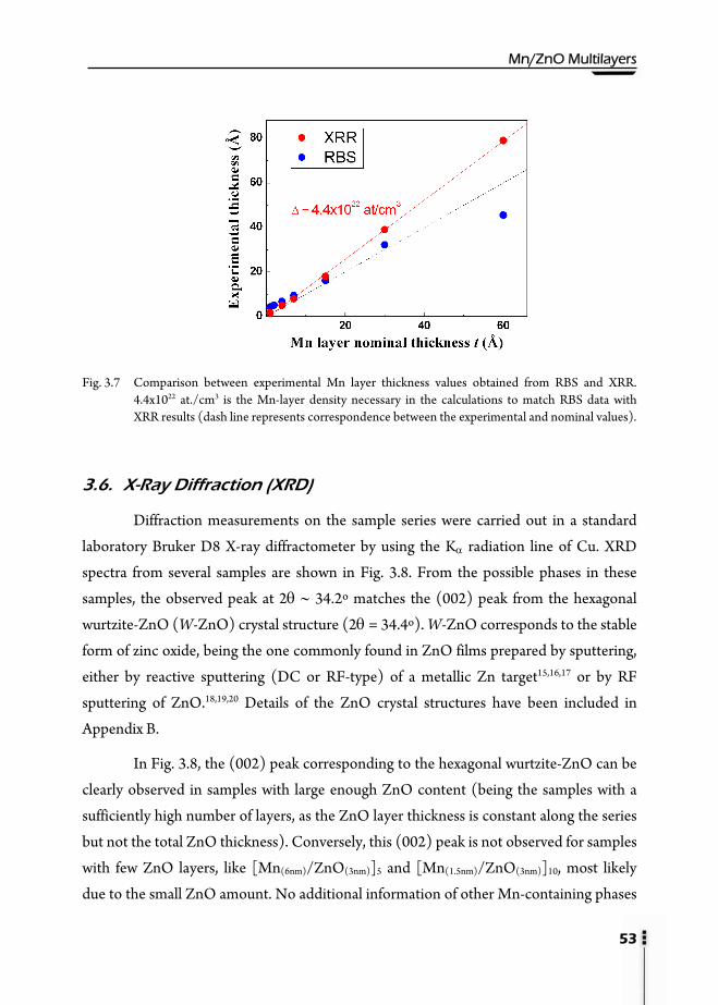
Mn/ZnO Multilayers
53
Fig. 3.7 Comparison between experimental Mn layer thickness values obtained from RBS and XRR.
4.4x10²² at./cm3 is the Mn-layer density necessary in the calculations to match RBS data with XRR results (dash line represents correspondence between the experimental and nominal values).
3.6. X-Ray Diffraction (XRD)
Diffraction measurements on the sample series were carried out in a standard
laboratory Bruker D8 X-ray diffractometer by using the Kα radiation line of Cu. XRD
spectra from several samples are shown in Fig. 3.8. From the possible phases in these
samples, the observed peak at 2θ ∼ 34.2º matches the (002) peak from the hexagonal
wurtzite-ZnO (W-ZnO) crystal structure (2θ = 34.4º). W-ZnO corresponds to the stable
form of zinc oxide, being the one commonly found in ZnO films prepared by sputtering,
either by reactive sputtering (DC or RF-type) of a metallic Zn target15,16,17 or by RF
sputtering of ZnO.18,19,20 Details of the ZnO crystal structures have been included in
Appendix B.
In Fig. 3.8, the (002) peak corresponding to the hexagonal wurtzite-ZnO can be
clearly observed in samples with large enough ZnO content (being the samples with a
sufficiently high number of layers, as the ZnO layer thickness is constant along the series
but not the total ZnO thickness). Conversely, this (002) peak is not observed for samples
with few ZnO layers, like [Mn(6nm)/ZnO(3nm)]5 and [Mn(1.5nm)/ZnO(3nm)]10, most likely
due to the small ZnO amount. No additional information of other Mn-containing phases
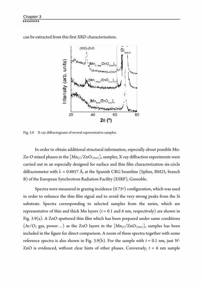
CChhaapptteerr 33
can be extracted from this first XRD characterization.
Fig. 3.8 X-ray diffractograms of several representative samples.
In order to obtain additional structural information, especially about possible Mn-
Zn-O mixed phases in the [Mn(t)/ZnO(3nm)]n samples, X-ray diffraction experiments were
carried out in an especially designed for surface and thin film characterization six-circle
diffractometer with λ = 0.8857 Å, at the Spanish CRG beamline (Spline, BM25, branch
B) of the European Synchrotron Radiation Facility (ESRF), Grenoble.
Spectra were measured in grazing incidence (0.75º) configuration, which was used
in order to enhance the thin film signal and to avoid the very strong peaks from the Si
substrate. Spectra corresponding to selected samples from the series, which are
representative of thin and thick Mn layers (t = 0.1 and 6 nm, respectively) are shown in
Fig. 3.9(a). A ZnO sputtered thin film which has been prepared under same conditions
(Ar/O2 gas, power…) as the ZnO layers in the [Mn(t)/ZnO(3nm)]n samples has been
included in the figure for direct comparison. A zoom of these spectra together with some
reference spectra is also shown in Fig. 3.9(b). For the sample with t = 0.1 nm, just W-
ZnO is evidenced, without clear hints of other phases. Conversely, t = 6 nm sample

Mn/ZnO Multilayers
55
spectrum confirms the presence of cubic MnO rocksalt (RS) nanocrystals, evidenced by
its (200)-RS peak at about 23º. The broad peak at about 19.5º might correspond to
(002)-W and (111)-RS peaks.
Therefore, in agreement with the previous XRR and RBS comparison, which
indicated the presence of Mn partially oxidized in the samples, MnO nanocrystals have
been identified in the t = 6 nm sample by high resolution grazing incidence X-ray
diffraction.
Fig. 3.9 (a) Grazing incidence (ω = 0.75º) X-ray diffraction of several studied multilayers and a 70 nm sputtered ZnO film. (b) Zoom of the grazing incidence sample spectra in comparison with XRD patterns from W-ZnO and RS-MnO references.
The θ-2θ scan of the t = 0.1 nm sample in comparison with the sputtered ZnO
film is shown in Fig. 3.10, where it can be inferred that samples exhibit texture. The ZnO

CChhaapptteerr 33
grain size of several samples from the series (shown in Table 3.IV) has been obtained
using the Scherrer formula and the Gaussian fits of the (002)-ZnO peaks. Gaussian fits of
several ZnO diffraction peaks are shown in Fig. 3.10(b).
10 20 30
17 18 19 20 21 22
Inte
nsity
(arb
. uni
ts)
θ−2θ scan
t = 0.1 nm t = 6 nm ZnO thin film
2θ (º)
(400)-Si subs
(a)
(200)-Si subs
x 3
Inte
nsity
(arb
. uni
ts)
t = 0.1 nm t = 6 nm ZnO thin film Gaussian fits
2θ (º)
(002)-ZnO
(101)-ZnO
(200)-Si subs
(b)
x 3
Fig. 3.10 (a) θ-2θ X-ray diffraction measurements of t = 0.1 nm sample and a 70 nm sputtered ZnO film.
(b) Zoom of the same θ-2θ X-ray diffraction spectra and their corresponding Gaussian fits.
- In the case of samples with larger t, the size of these nanocrystalline grains is near 3
nm, which is of the order of the ZnO layer thickness. This suggests that, even if
interdiffusion is expected, deposited Mn is actually present as a continuous Mn
oxide layer, interrupting the ZnO grain growth in the out-of-plane direction. On
the other hand, no traces of metallic Mn or other Mn-Zn-O phases have been found.
- In the case of samples with very thin Mn layers, the obtained crystalline grain sizes
are above 7 nm, which are considerably higher than the 3 nm ZnO layer nominal
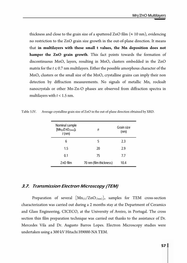
Mn/ZnO Multilayers
57
thickness and close to the grain size of a sputtered ZnO film (≈ 10 nm), evidencing
no restriction to the ZnO grain size growth in the out-of-plane direction. It means
that in multilayers with these small t values, the Mn deposition does not
hamper the ZnO grain growth. This fact points towards the formation of
discontinuous MnOx layers, resulting in MnOx clusters embedded in the ZnO
matrix for the t ≤ 0.7 nm multilayers. Either the possible amorphous character of the
MnOx clusters or the small size of the MnOx crystalline grains can imply their non
detection by diffraction measurements. No signals of metallic Mn, rocksalt
nanocrystals or other Mn-Zn-O phases are observed from diffraction spectra in
multilayers with t < 1.5 nm.
Table 3.IV. Average crystalline grain size of ZnO in the out-of-plane direction obtained by XRD.
Nominal sample [Mn(t)/ZnO(3nm)]n
t (nm) n Grain size
(nm)
6 5 2.3
1.5 20 2.9
0.1 75 7.7
ZnO film 70 nm (film thickness) 10.4
3.7. Transmission Electron Microscopy (TEM)
Preparation of several [Mn(t)/ZnO(3nm)]n samples for TEM cross-section
characterization was carried out during a 2 months stay at the Department of Ceramics
and Glass Engineering, CICECO, at the University of Aveiro, in Portugal. The cross
section thin film preparation technique was carried out thanks to the assistance of Dr.
Mercedes Vila and Dr. Augusto Barros Lopes. Electron Microscopy studies were
undertaken using a 300 kV Hitachi H9000-NA TEM.
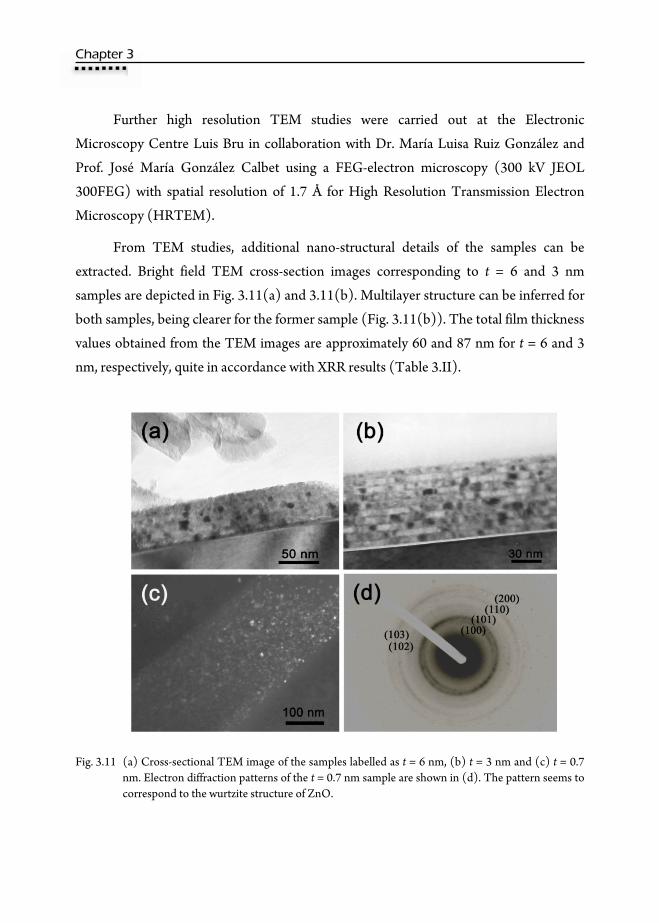
CChhaapptteerr 33
Further high resolution TEM studies were carried out at the Electronic
Microscopy Centre Luis Bru in collaboration with Dr. María Luisa Ruiz González and
Prof. José María González Calbet using a FEG-electron microscopy (300 kV JEOL
300FEG) with spatial resolution of 1.7 Å for High Resolution Transmission Electron
Microscopy (HRTEM).
From TEM studies, additional nano-structural details of the samples can be
extracted. Bright field TEM cross-section images corresponding to t = 6 and 3 nm
samples are depicted in Fig. 3.11(a) and 3.11(b). Multilayer structure can be inferred for
both samples, being clearer for the former sample (Fig. 3.11(b)). The total film thickness
values obtained from the TEM images are approximately 60 and 87 nm for t = 6 and 3
nm, respectively, quite in accordance with XRR results (Table 3.II).
Fig. 3.11 (a) Cross-sectional TEM image of the samples labelled as t = 6 nm, (b) t = 3 nm and (c) t = 0.7
nm. Electron diffraction patterns of the t = 0.7 nm sample are shown in (d). The pattern seems to correspond to the wurtzite structure of ZnO.

26
pa
rin
no
a r
fro
M
ele
po
in
Th
pe
alo
RS
Dark field
60 nm of total
attern of this sa
ngs can be relat
oticed that the e
reliable indexati
om XRD (see F
Mn layer thickne
ectron diffracti
olycrystalline gr
TEM imag
the image depi
he HREM stu
eriodicities and
ong [011] zone
S phase in the t
image of the t =thickness is in
ample (t = 0.7 n
ted to the polyc
existence of poo
ion of the rings.
Figs. 3.8-3.10),
ess. Although st
on rings, the p
rains in the t = 0
ge of the t = 3 n
icted in Fig. 3.1
udy indicates
their correspon
e axis. Therefor
t = 3 nm sampl
= 0.7 nm sample
n agreement wit
nm) is shown i
crystalline natur
orly defined ring
. Nonetheless, t
W-ZnO presen
rong evidences
pattern seems t
.7 nm sample (F
nm sample evide
12(a) as well as
the presence
nding FFT, fit w
re, HREM evid
e.
e is shown in Fig
th XRR results
in Fig. 3.11(d),
re of the t = 0.7
gs with slightly o
aking into consi
nce is expected
could not be in
to match with
Fig. 3.11(d)).
ences the presen
its nanocrystall
of nanocrystal
with a cubic NaC
dences the pre
Mn/ZnO
g. 3.11(c). The
. The electron
, where the app
7 nm sample. It
oval shapes mak
ideration the ab
in this sample
nferred from th
the existence
nce of 10 layers
line nature (Fig
ls (Fig. 3.12(
Cl type (rocksa
sence of nano
Multilayers
59
obtained ∼
diffraction
pearance of
t should be
kes difficult
bove results
with small
he obtained
of W-ZnO
s (as shown
g. 3.12(b)).
c)) whose
lt) unit cell
crystalline

CChh
Fig
hhaapptteerr 33
g. 3.12 Cross-sectiional TEM (a) andd (b), and HRTEMM (c) images of the
t = 3 nm sample.
Mn/ZnO Multilayers
61
3.8. X-Ray Absorption Spectroscopy (XAS)
Mn electronic states and local structure of the Mn/ZnO multilayers have been
investigated by means of X-ray absorption spectroscopy. XAS experiments were carried
out at the BM25 beamline (SpLine) of the European Synchrotron Radiation Facility
(ESRF), Grenoble. Several spectra were collected in order to improve statistics and to
have a good signal to noise ratio. The fluorescence spectra were obtained at room
temperature under a configuration where the detector formed an angle of 90º respect to
the incoming beam. Further experimental details can be found in section 2.6.1.
3.8.1. X-Ray Absorption Near-Edge Spectroscopy (XANES)
XANES experiments were performed in order to obtain information on the
manganese charge state.
Mn K-edge XANES spectra of the samples series in comparison with a Mn metal
foil and MnO2 are displayed in Fig. 3.13. The Mn absorption K-edge energy was
calibrated by measuring a Mn foil and setting its E0 value as in Ref. [21] to be compared
with the reported relative edge positions of the Mn compounds with different oxidation
states. After edge jump normalization, direct comparisons can be made among the
XANES spectra for all samples. The most important fact is that the sample series spectra
exhibit a shift of the main edge energy, higher than 3.5 eV, from the thickest Mn-layer
sample (t = 6 nm) to the thinnest one (t = 0.1 nm), indicating an increase of the
oxidation state as the Mn-layer thickness decreases. Arrows have been plotted at the
threshold energy in Fig. 3.13.
Edge-energy values instead of pre-edge or white-line features have been used here
to obtain the average Mn oxidation state, since for the obtained data this approach is
more sensitive to Mn valence and less sensitive to structural effects. Taking into account
the linear relationship between threshold energy and oxidation state for the reference
compounds,21 the average oxidation state of Mn in these multilayered samples can be easily determined by measuring the threshold energy (inset of Fig. 3.13).

CChhaapptteerr 33
6536 6540 6544 65480
1
2
3
4
6530 6540 6550 6560 6570 6580 6590
Mn
vale
nce
Energy (eV)
Metallic Mn
MnO
MnO2
MnOOH
Samples
E 0=
6535
.7 e
V
Nor
mal
ized
Abs
orpt
ion
(arb
. uni
ts)
t = 1.5 nm
Energy (eV)
t = 6 nm
t = 3 nm
Mn metal
MnO2
t = 0.7 nm
t = 0.4 nm
t = 0.1 nm
Mn K-edge
Fig. 3.13 Mn K-edge spectra of the samples compared with Mn foil and MnO2. The inset shows the
evolution of the Mn oxidation state compared with Mn0, Mn2+ (MnO), Mn3+ (MnOOH) and Mn4+ (MnO2) references.21
It is worth to comment that in manganese oxides, the threshold energy values
obtained from the maximum of the first derivative, results to be troubled by the splitting
of the 1s-4p transition,22 which affects to the first maximum position of the first
derivative. For this reason, the threshold energy has been estimated in all cases as the
energy corresponding to one third of the jump. Results, summarized in Table 3.V,
indicate a variation of the average Mn oxidation state with t, ranging the Mn
oxidation states between Mn2+ and Mn4+. Samples with larger t in the series are related
to Mn valence near to +2, while the ones with small t values present oxidation states
higher than +3. It is important to remark that under the experimental measuring
conditions, the entire depth of the film is explored, contributing all Mn atoms from each
sample to the Mn K-edge XAS signal. It means that the obtained oxidation state value
corresponds to the average of the actual distribution present in the whole film.
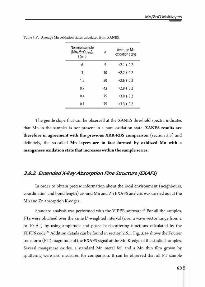
Mn/ZnO Multilayers
63
Table 3.V. Average Mn oxidation states calculated from XANES.
Nominal sample [Mn(t)/ZnO(3nm)]n
t (nm) n Average Mn
oxidation state
6 5 +2.1 ± 0.2
3 10 +2.2 ± 0.2
1.5 20 +2.6 ± 0.2
0.7 43 +2.9 ± 0.2
0.4 75 +3.0 ± 0.2
0.1 75 +3.3 ± 0.2
The gentle slope that can be observed at the XANES threshold spectra indicates
that Mn in the samples is not present in a pure oxidation state. XANES results are
therefore in agreement with the previous XRR-RBS comparison (section 3.5) and
definitely, the so-called Mn layers are in fact formed by oxidized Mn with a
manganese oxidation state that increases within the sample series.
3.8.2. Extended X-Ray Absorption Fine Structure (EXAFS)
In order to obtain precise information about the local environment (neighbours,
coordination and bond length) around Mn and Zn EXAFS analysis was carried out at the
Mn and Zn absorption K-edges.
Standard analysis was performed with the VIPER software.23 For all the samples,
FTs were obtained over the same k2-weighted interval (over a wave vector range from 2
to 10 Å-1) by using amplitude and phase backscattering functions calculated by the
FEFF6 code.24 Addition details can be found in section 2.6.1. Fig. 3.14 shows the Fourier
transform (FT) magnitude of the EXAFS signal at the Mn K-edge of the studied samples.
Several manganese oxides, a standard Mn metal foil and a Mn thin film grown by
sputtering were also measured for comparison. It can be observed that all FT sample

CChhaapptteerr 33
spectra present a first peak at ∼1.5 Å. This contribution is compatible with a Mn-O
distance of about 2 Å, indicating the presence of oxidized Mn in the samples, in
agreement with XANES studies. A noticeable difference between the FT magnitude of
samples with thicker Mn layers (t = 6, 3 nm) and the other samples with thinner Mn
layers can be observed in the graph.
Fig. 3.14 Experimental EXAFS Fourier Transforms (FT) of the Mn/ZnO multilayer samples. FT of
manganese oxides, a Mn foil and a Mn sputtered thin film are shown for comparison.
The position and shape of the FT peaks for samples with t = 6, 3 nm clearly differ
from the corresponding to samples with t ≤ 1.5 nm, all of them very similar, evidencing
differences in the structural properties between these two samples with thicker Mn layers
and the others. From the magnetic measurements, a noticeable difference was also
observed between the magnetic behaviour of these two samples and the others.
Multilayers with t ≥ 3 nm exhibit ferromagnetic behaviour over room temperature while
for samples with t below this value the paramagnetic contribution increases and the
magnitude of magnetization becomes negligible. This fact suggests a direct relation
between the ferromagnetic behaviour of these samples and the different Mn local
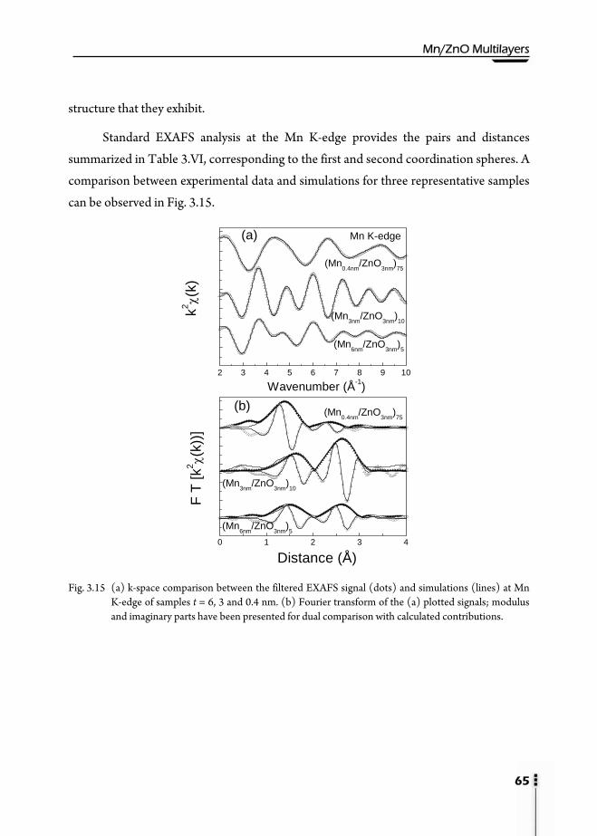
Mn/ZnO Multilayers
65
structure that they exhibit.
Standard EXAFS analysis at the Mn K-edge provides the pairs and distances
summarized in Table 3.VI, corresponding to the first and second coordination spheres. A
comparison between experimental data and simulations for three representative samples
can be observed in Fig. 3.15.
0 1 2 3 4
2 3 4 5 6 7 8 9 10
F T
[k2 χ(
k))]
Distance (Å)
(Mn6nm/ZnO3nm)5
(Mn3nm/ZnO3nm)10
(Mn0.4nm/ZnO3nm)75(b)
k2 χ(k)
Wavenumber (Å-1)
(Mn6nm/ZnO3nm)5
(Mn3nm/ZnO3nm)10
(Mn0.4nm/ZnO3nm)75
(a) Mn K-edge
Fig. 3.15 (a) k-space comparison between the filtered EXAFS signal (dots) and simulations (lines) at Mn
K-edge of samples t = 6, 3 and 0.4 nm. (b) Fourier transform of the (a) plotted signals; modulus and imaginary parts have been presented for dual comparison with calculated contributions.

CChhaapptteerr 33
TABLE 3.VI. Summary of XAS results corresponding to references and samples: Average Mn oxidation states and R, N, σ2 EXAFS parameters (distance (R), number of neighbours (N) and the Debye-Waller factor, respectively). ∗ M stands for both Mn or Zn.
References Mn oxid.state Pair R
(Å) N
MnO +2 Mn-O 2.22 6 Mn-Mn 3.14 12
Mn3O4 +2 Mn-O 2.04 4 +3 Mn-O 1.93 4 2.28 2
Mn2O3 +3 Mn-O 1.89-2.25 6 β-MnO2 +4 Mn-O 1.89 6
Mn-Mn 2.89 2 Mn-Mn 3.40 8
ZnO Zn-O 1.99 4 Zn-Zn 3.23 12
Samples Mn oxid.state Pair ∗ R
(Å) N σ2 (10-3Å2)
sputtered ZnO film Zn-O 1.97±0.02 4 0.4±0.5 Zn-Zn 3.18±0.02 12 12±1
[Mn6nm/ZnO3nm]5 +2.1±0.2 Mn-O 2.03±0.02 1.7 4±0.5 Mn-O 2.18±0.02 1.6 5±0.5 Mn-M 3.11±0.02 4.3 15±1 Mn-M 3.37±0.02 4.0 18±1 Zn-O 1.98±0.02 4.5 18±0.5 Zn-M 3.12±0.02 7.5 17±1 Zn-M 3.37±0.02 4.0 6±1
[Mn3nm/ZnO3nm]10 +2.2±0.2 Mn-O 2.16±0.02 5.0 8±0.5 Mn-M 3.12±0.02 7.3 11±1 Mn-M 3.37±0.02 2.7 9±1
[Mn1.5nm/ZnO3nm]20 +2.6±0.2 Mn-O 1.94±0.02 3.6 2.5±0.5 Mn-M 2.86±0.02 1.6 20±1 Zn-O 2.05±0.02 2.9 1.4±0.5 Zn-Zn 3.14±0.02 5.0 4.5±1
[Mn0.7nm/ZnO3nm]43 +2.9±0.2 Mn-O 1.92±0.02 2.9 3±0.5 Mn-M 2.91±0.02 1.9 30±1
[Mn0.4nm/ZnO3nm]75 +3.0±0.2 Mn-O 1.91±0.02 4.5 2.5±0.5 Mn-M 2.88±0.02 1.0 50±1
[Mn0.1nm/ZnO3nm]75 +3.3± 0.2 Mn-O 1.93±0.02 4.5 5±0.5 Mn-M 2.91±0.02 1.0 40±1
Mn/ZnO Multilayers
67
From the obtained results and in agreement with XANES data, shorter Mn-O
distances are achieved for thinner Mn-layer samples, evidencing higher Mn oxidation
states in the samples with t ≤ 1.5 nm. For all these films the local environment around
Mn is very similar. Mn-O and Mn-Mn obtained distances present values of 1.91 - 1.94 Å
and 2.86 – 2.91 Å, respectively, which are very close to those in β-MnO2 structure.25 Both,
the high Mn oxidation state and the pair distances (RMn-O ∼ 1.92 Å and RMn-Mn ∼ 2.9 Å)
indicate mostly MnO2 formation in samples with very thin Mn layers.
It should be commented that direct comparison between the FT corresponding to
films with t < 1.5 nm and MnO2 reference does not match in magnitude for the second
coordination sphere. The small magnitude observed for the peaks corresponding to
second coordination spheres is, almost certainly, due to the very small MnO2 grains
obtained in the small Mn layers. This fact makes a significant reduction of the
coordination number for coordination spheres further than the first one,26 which
provides an amorphous-like FT magnitude. For that reason, even if second FT peaks are
not comparable in magnitude, the second peak position for samples with t < 1.5 nm
matches with MnO2 since the fitted distances, given in Table 3.VI, do.
Conversely and also in agreement with XANES results, in the case of samples with
t ≥ 3 nm, the obtained Mn-O distances (RMn-O ∼ 2.1 Å) and the revealed average Mn
oxidation state near Mn2+ match with MnO formation when comparing with MnO
reference, where RMn-O ∼ 2.2 Å. Following a more refined EXAFS analysis, it is found that
the t = 3 nm sample presents mostly one Mn-O contribution at RMn-O = 2.16 Å, while for
the t = 6 nm sample, two different Mn-O distances are provided by the fit, being 2.03 and
2.18 Å. Fits of both samples also show second neighbour distances RMn-M ∼ 3.1 Å and
RMn-M ∼ 3.4 Å, being M = Mn, Zn. It is important to underline that, for the analysed k-
range interval, no significant differences were obtained when considering Mn or Zn as
backscatterer atoms. It means that, at least under the achieved experimental conditions,
there is no possibility to fairly distinguish between them (for this reason, only a RMn-M
distance contribution is reported, where M stands for either Mn or Zn).
Regarding the EXAFS analysis of these multilayers with larger t values (t ≥ 3 nm) it
should be considered that on one hand, MnO formation has been evidenced by the
CChhaapptteerr 33
above XRD and HRTEM experiments. Therefore, MnO phase, which has a rocksalt-type
structure (RS), with octahedral Mn coordination (Oh), is expected to be detected by
EXAFS.
In addition, diffusion of Mn cations into the close ZnO layers could be also
possible in these samples and consequently, the presence of Mn in the ZnO wurtzite (W)
structure, with tetrahedral Mn coordination (Td) might be found. Hence, stabilization of
a labelled Zn-O-Mn mixed phase (W-type) at the ZnO rich regions should be also
considered in the analysis.
On the other hand, diffusion of Zn cations into the MnO phase should be also
taken into account. In fact, it must be noted that, although it is well known that the
hexagonal wurtzite (W) is the stable form of ZnO, under specific conditions, like high
pressure, the cubic rocksalt phase (RS) could be induced for ZnO. (More details of the
W to RS phase transitions in ZnO are included in Appendix B). When the relative
content of Mn in ZnO phase is high, an enhanced stability of this rocksalt phase is
expected since RS is the stable form of MnO. Therefore, stabilization of a mixed phase
named as Mn-O-Zn (RS-type) at the MnO-rich regions seems in fact quite probable.i
All these points should be considered when analysing the complicated EXAFS
results obtained for the samples with larger t values (t ≥ 3 nm), where the complex
situation of non-homogenously intermixed layers with coexistence of Zn-Mn-O mixed
phases having both W and RS structures, maybe expected.
The obtained results for the t = 3 nm sample are well in agreement with RS
structure: the obtained RMn-O = 2.16 Å is slightly smaller than the corresponding to the
pure MnO rocksalt (2.22 Å) but it is in full agreement with the obtained distance (2.17
Å) by EXAFS in Zn1-xMnxO thin films with RS-stabilized structure reported by Pellicer-
Porres et al.,9 what supports the existence of Mn-O-Zn (RS) mixed phase. In addition,
second neighbours, found at RMn-M = 3.11 Å, match the geometrical condition between i Notice that “Zn-O-Mn (W)” refers to the mixed phase with Mn diffused into the majority W-ZnO phase while “Mn-O-Zn (RS)” refers
to the mixed phase with Zn diffused into the majority RS-MnO phase. “Zn-Mn-O mixed phases” refer to both.

Mn/ZnO Multilayers
69
first and second distances in rocksalt structure ( 2 ratio). Besides, there is a minor
contribution with RMn-M = 3.37 Å, that also appears in the t = 6 nm sample, and that will
be explained below.
Results for the t = 6 nm sample indicate the same distance contributions as t = 3
nm sample corresponding to RS structure, but in addition, EXAFS analysis shows here
extra contributions with distances RMn-O = 2.03 Å and RMn-M = 3.37 Å, that can be
identified by Mn substituting Zn in wurtzite phase.9,27 The obtained Mn-O distance is
slightly larger than Zn-O in wurtzite structure, what is in fact expected since the Mn2+
ionic radius is higher than the Zn2+ one. In addition, this distance coincides again with
the EXAFS obtained value in Zn1-xMnxO thin films9 with low Mn content and wurtzite
phase (that we have labelled as Zn-O-Mn (W)). Not much attention should be paid to
the obtained coordination numbers for these samples (especially for the second shell);
its high correlation with the Debye-Waller factors, the small grain size effect as well as
experimental difficulties due to self-absorption and short available k-space can
considerably increase its own uncertainty.
Additional measurements were performed at the Zn K-edge of several samples.
Fig. 3.16 shows the Fourier transform magnitude of two samples (t = 6, 1.5 nm) and a
ZnO sputtered film. The evaluation of the Zn-environment in the t = 1.5 sample and the
ZnO sputtered film by comparing its corresponding FT shape should be made just in its
wide sense. On one hand, the signal to noise ratio is lower here than in the Mn K-edge.
Moreover, the ZnO layers thickness in these samples are only 3 nm, what allows finite
size effects and besides, strains in the samples seem likely (a slightly shifted (002)-ZnO
peak was found in section 3.6), having both influence on the TF magnitude.
Standard EXAFS analysis provides Zn-O and Zn-M pairs and distances
summarized in Table 3.VI, corresponding to the first and second coordination spheres.
Experimental data and simulations for the Fourier transform and back Fourier transform
of the EXAFS signal at the Zn K-edge are shown in Fig. 3.17.

CChhaapptteerr 33
0 1 2 3 4 5 6 7 8
F T
[k2 χ(
k)]
Distance (Å)
(Mn6nm/ZnO3nm)5
(Mn1.5nm/ZnO3nm)20
ZnO
Zn K-edge
Fig. 3.16. Fourier Transforms (FT) of Zn K-edge EXAFS oscillation function k2χ(k) of samples t = 6, 1.5
nm and a 100 nm ZnO film.
It can be observed that in the case of the t = 6 nm sample, the second peak of the
FT magnitude reveals a second-neighbour contribution at higher atomic distances. Data
analysis provides an additional Zn-M contribution at 3.37 Å. This distance is in full
agreement with the Mn-M contribution found in the Mn K-edge analysis of the
multilayer samples with t > 1.5 nm. Both results put together indicate that this sample is
composed by layers containing Mn in both, wurtzite and rocksalt phases in the t = 6 nm
sample. Therefore, distances corresponding to W-ZnO, Zn-O-Mn (W) and MnO (RS)
have been found by EXAFS analysis of the t = 6 nm sample. The non-detection at the Zn
K-edge of Zn-O contribution at distances ∼ 2.1 Å, which would be related to Mn-O-Zn
(RS) phase, can be assigned to the short available k-range as well as the small fraction of
Zn in the Mn-O-Zn phase compared to the majority of Zn in W-ZnO phase. A small
amount of Mn-O-Zn (RS) phase in comparison with Zn-O-Mn (W) phase is
consequently expected for the t = 6 nm sample.
The situation is different for the t = 3 nm sample, where the Mn-O distance
corresponding to Mn in W-ZnO phase is not detected (although Mn-M contribution is
observed at 3.37 Å, exactly as for the t = 6 nm sample). The non distinction between the
two similar Mn-O distances expected in the t = 3 nm sample is, in all likelihood, due to

Mn/ZnO Multilayers
71
the low fraction of Zn-O-Mn (W) compared to RS phase. Small amount of Zn-O-Mn
(W) phase in comparison with RS phase is therefore expected for the t = 3 nm sample.
Fig. 3.17 (a) k-space comparison between the filtered EXAFS signal (dots) and simulations (lines) at Mn K-edge of samples t = 6, 1.5 nm and a 100 nm ZnO film. (b) Fourier transform of the (a) plotted signals; modulus and imaginary parts have been presented for dual comparison with calculated contributions (lines).
Summarizing these results, the complex EXAFS analysis of the samples with t ≥ 3
nm indicates the formation of Zn-Mn-O mixed phases in non-homogenously intermixed
layers, where MnO-rich phase (RS), named as Mn-O-Zn and ZnO-rich phase (W),
named as Zn-O-Mn, coexist. For the t = 6 nm sample, majority of W mixed phase in
comparison with the RS phase is evidenced, while the opposite occurs for the t = 3 nm
sample. The obtained EXAFS distances fully agree with the ones reported by Pellicer et

CChhaapptteerr 33
al.9 for Zn1-xMnxO thin films with W or RS-stabilized structures.
The analysis is much more simple for samples with t < 1.5 nm, where mostly
MnO2 formation inside W-ZnO is identified. The sample with t = 1.5 nm, laying in the
barrier between both different situations, shows similarities with both behaviours, being
closer to the t ≤ 0.7 nm one.
3.9. Structural and magnetic scheme
According to the growth conditions, the following model is proposed to explain all
the obtained results. For all the samples, the oxygen excess at the surface of the lately
deposited ZnO layer can provide a highly oxidized state to the very close Mn atoms and
therefore, a very small Mn4+ fraction might be expected at the first growth stage of the
Mn layers.
For samples with very thin Mn layers, no appreciable differences are expected
between top and bottom of the Mn layer, leading to the formation of MnO2 in the entire
non-continuous layer. The formation of MnO2 nano-clusters inside the ZnO matrix has
been evidenced jointly by XRR simulations, X-ray diffraction and EXAFS results. Either
the amorphous character of the MnO2 clusters or the small size of its crystalline grains
(indicated by their EXAFS amorphous-like FT magnitudes) implies their non detection
by diffraction measurements. The tendency of MnO2 to be present in a non-
stoichiometric state with Mn4+ vacancies, Mn3+ replacing Mn4+ cations and OH- species
replacing O2- anions explains the obtained oxidation states smaller than +4 obtained by
XANES. Nonetheless, the presence of small Mn3+ contribution could be also expected. In
this case of small t values, due to big differences in the ionic radii, neither Mn4+ diffusion
into ZnO nor Zn2+ diffusion in MnO2 are expected28. Consequently, for t ≤ 0.7 nm, all the
obtained results indicate the formation of mostly amorphous MnO2 grains inside the W-
ZnO matrix, presenting these samples paramagnetic-like behaviour. A scheme of the
situation is represented in Fig. 3.18 (right).
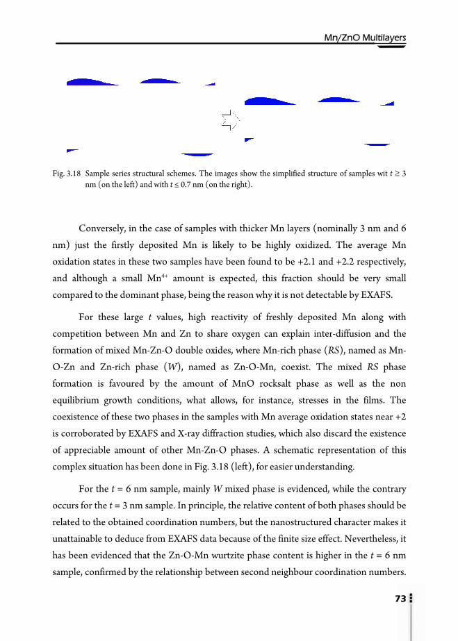
Fig
nm
ox
an
co
co
fo
O
fo
eq
co
is
of
co
oc
re
un
ha
sa
g. 3.18 Sample sernm (on the
Conversely
m) just the firs
xidation states i
nd although a
ompared to the d
For these
ompetition betw
rmation of mix
-Zn and Zn-ri
rmation is fav
quilibrium grow
oexistence of the
corroborated b
f appreciable am
omplex situation
For the t =ccurs for the t =
lated to the obt
nattainable to d
as been evidenc
mple, confirme
ries structural schee left) and with t ≤
y, in the case of
stly deposited
n these two sam
small Mn4+ am
dominant phase
large t values
ween Mn and Z
ed Mn-Zn-O d
ich phase (W)
voured by the
wth conditions,
ese two phases
by EXAFS and X
mount of other
n has been done
= 6 nm sample,
3 nm sample. I
tained coordina
educe from EXA
ced that the Zn-
ed by the relatio
emes. The images s0.7 nm (on the righ
f samples with t
Mn is likely t
mples have been
mount is expec
e, being the reas
, high reactivit
Zn to share ox
ouble oxides, w
, named as Zn
amount of M
, what allows,
in the samples w
X-ray diffraction
r Mn-Zn-O ph
e in Fig. 3.18 (le
mainly W mixe
n principle, the
ation numbers, b
AFS data becau
-O-Mn wurtzite
nship between
show the simplifiedht).
thicker Mn laye
to be highly ox
n found to be +
cted, this fracti
son why it is not
ty of freshly d
xygen can expla
where Mn-rich p
n-O-Mn, coexi
nO rocksalt ph
for instance, s
with Mn averag
n studies, which
ases. A schema
eft), for easier un
ed phase is evid
relative conten
but the nanostru
use of the finite
e phase content
second neighbo
Mn/ZnO
d structure of sam
ers (nominally 3
xidized. The av
+2.1 and +2.2 re
ion should be
t detectable by E
deposited Mn
ain inter-diffusio
phase (RS), nam
ist. The mixed
hase as well a
stresses in the
ge oxidation sta
h also discard th
atic representat
nderstanding.
denced, while th
nt of both phase
uctured charact
size effect. Neve
t is higher in th
our coordination
Multilayers
73
mples wit t ≥ 3
3 nm and 6
verage Mn
espectively,
very small
EXAFS.
along with
on and the
med as Mn-
d RS phase
as the non
films. The
tes near +2
he existence
tion of this
he contrary
s should be
ter makes it
ertheless, it
he t = 6 nm
n numbers.

CChhaapptteerr 33
It is worth to note that, unfortunately, the low relative ratio of Zn-O-Mn wurtzite phase
wurtzite mixed phase in the t = 3 nm sample does not allow to resolve the two similar
Mn-O distances expected.
Finally, in order to prove the validity of this model, the multilayer XANES spectra
with large t values should be fitted by a linear combination of the XANES spectra
corresponding to Mn in each different phase, wurtzite and rocksalt, whose relative
content would be obtained from the fit.
Fig. 3.19 shows the fits of XANES spectra of samples t = 6 and 3 nm. Spectra of
Mn in RS (Mn in Oh coordination) and Mn in W (Mn in Td coordination) phases used as
references (thick solid lines) have been taken from experimental data in Ref. 9, where
both phases were obtained in the Mn-Zn-O system under transformation induced by
hydrostatic pressure.
First of all, it is important to note an experimental hint that comes from the pre-
edge peak. The existence of this pre-edge (at 6537 eV in Fig. 3.19) indicates tetrahedral
(Td) coordination since it is related to p-d hybridization, which is allowed when the Mn
site symmetry does not present an inversion center, as in Td configuration. This pre-edge
peak loses most of its intensity in the RS phase, with octahedral symmetry (Oh), since it
contains an inversion center.9 The clear existence of this pre-peak for t = 6 nm sample,
with majority of W phase, as well as the considerable decrease of the pre-peak intensity
for t = 3 nm sample should be underlined here, sustaining the obtained EXAFS results.
Finally, as it can be observed in Fig. 3.19, just by linear combination of Mn
replacing Zn into the W and RS phases, the experimental spectra are quite well
reproduced, fact that corroborates the coexistence of these two phases for t ≥ 3 nm
samples. The obtained relative content of both phases are [RS] = 25% and [W] = 75% for
the t = 6 nm sample and [RS] = 70 % and [W] = 30 % for the t = 3 nm one.
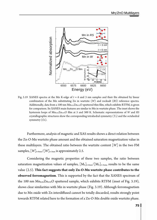
Mn/ZnO Multilayers
75
6550 6575 6600 6625 6650
-50 -25 0 25 50-40
-20
0
20
40
Nor
mal
ized
abs
orpt
ion
Energy (eV)
Mn in RS
Mn in W
Mn0.05Zn0.95O film
t = 3 nm
t = 6 nm
M (e
mu/
cm3 )
H (kOe)
T = 5 K
T = 300 K
Fig. 3.19 XANES spectra at the Mn K-edge of t = 6 and 3 nm samples and their fits obtained by linear
combination of the Mn substituting Zn in wurtzite (W) and rocksalt (RS) reference spectra. Additionally, data from a 100 nm Mn0.05Zn0.95O sputtered thin film, which exhibits RTFM, is given for comparison. Its XANES main features are similar to Mn in wurtzite phase. The inset shows the hysteresis loops of Mn0.05Zn0.95O film at 5 and 300 K. Schematic representations of W and RS crystallographic structures show the corresponding tetrahedral symmetry (Td) and the octahedral symmetry (Oh).
Furthermore, analysis of magnetic and XAS results shows a direct relation between
the Zn-O-Mn wurtzite phase amount and the obtained saturation magnetization value in
these multilayers. The obtained ratio between the wurtzite content [W] in the two FM
samples, [W]t=6nm/[W]t=3nm is approximately 2.5.
Considering the magnetic properties of these two samples, the ratio between
saturation magnetization values of samples, [MS]t=6nm/[MS]t=3nm, results to be the same
value (2.5). This fact suggests that only Zn-O-Mn wurtzite phase contributes to the
observed ferromagnetism. This is supported by the fact that the XANES spectrum of
the 100 nm Mn0.05Zn0.95O sputtered sample, which exhibits RTFM (inset of Fig. 3.19),
shows clear similarities with Mn in wurtzite phase (Fig. 3.19). Although ferromagnetism
due to Mn oxide with Zn interdiffused cannot be totally discarded, results strongly point
towards RTFM related here to the formation of a Zn-O-Mn double oxide wurtzite phase.

CChhaapptteerr 33
Despite the fact that the obtained normalized Mn moments are very small, it should be
remarked that results indicate that not all the Zn-Mn-O phases contribute to
ferromagnetism. It means that normalizing to the total amount of Mn when calculating
magnetization values involves Mn moment values lower than the actual ones.
Recently, B. Gu et al.29 have performed quantum Monte Carlo calculations in the
p-type (Zn,Mn)O compound to determine how the crystal structure influences the
impurity bound state, which plays an important role in the development of the FM
correlations between the impurities. They have found that the FM correlations are
strongly influenced by the crystal structure. In particular, they have observed FM
correlations for wurtzite [W] and zinc-blenda [ZB] crystal structures, while no FM
correlations between the impurities have been found for the rocksalt [RS] structure.
3.10. Conclusions
Concerning the magnetic properties of these Mn multilayered systems, the main
conclusion of this chapter is the relevance of the Mn oxidation state in the diffusion
process and consequently in the magnetic properties of the films. The role that each
particular type of interface plays in the ferromagnetism of this Mn-Zn-O system has been
shown.
An evolution of the magnetic response depending on the Mn layer thickness (t)
has been observed within the sample series, where room temperature ferromagnetism
has been clearly found for [Mn(t)/ZnO(3nm)]n multilayers with larger values of t (nominally t = 6, 3 nm).
Different Mn electronic states within the sample series, depending on the Mn layer
thickness (t) have been revealed by XANES, showing that the average Mn oxidation state
ranges from +2.1 to +3.3. Diffraction studies agree with absence of metallic Mn in the
samples.

Mn/ZnO Multilayers
77
For Mn/ZnO samples with very thin Mn layers (t ≤ 0.7 nm), contrary to what it
was expected, X-ray absorption spectroscopy results have shown that Mn is not diluted
into the ZnO layers. Conversely, the formation of amorphous MnO2 nano-sized grains
inside the ZnO matrix has been evidenced together by XRR simulations, XAS and XRD
results. No sign of metallic Mn, rocksalt nanocrystals or other Mn-Zn-O phases is found.
For the obtained ferromagnetic samples (t ≥ 3 nm), EXAFS, XANES, HREM and
XRD results indicate the coexistence of Mn2+ in rocksalt and wurtzite phases. Non-
homogenously intermixed layers are expected, with Mn and Zn highly diffused into both
ZnO and MnO rich regions. In these samples showing FM, the obtained quantity of Mn
in [W] phase (Zn-O-Mn phase) scales with the saturation magnetization, pointing
towards this Zn-O-Mn double oxide wurtzite phase as the responsible of the observed
RTFM, in agreement with theoretical calculations.

CChhaapptteerr 33
References
1 D. C Kundaliya, S.B. Ogale, S.E. Lofland, S. Dhar, C.J. Metting, S.R. Shinde, Z. Ma, B.
Varughese, K.V. Ramanujachary, L. Salamanca-Riba, and T. Venkatesan, Nat. Mater. 3, 709 (2004).
2 M. A. García, M. L. Ruiz-González, A. Quesada, J. L. Costa-Krämer, J. F. Fernández, S. J. Khatib, A. Wennberg, A. C. Caballero, M. S. Martín-González, M. Villegas, F. Briones, J.M. González-Calbet, and A. Hernando, Phys. Rev. Lett. 94, 217206 (2005).
3 S. S. Yan, C. Ren, X. Wang, Y. Xin, Z. X. Zhou, L. M. Mei, M. J. Ren, Y.X. Chen, Y. H. Liu, and H. Garmestani, Appl. Phys. Lett. 84, 2376 (2004).
4 A. B. Pakhomov, B. K. Roberts, and K. M. Krishnan, Appl. Phys. Lett. 83, 4357 (2003).
5 J. C. A. Huang, H. S. Hsu, Y. M. Hu, C. H. Lee, Y. H. Huang, and M. Z. Lin, Appl. Phys. Lett. 85, 3815 (2004).
6 J. C. A. Huang, H. S. Hsu, J. H. Sun, S. L. Chiu, C. H. Lee, Y. F. Liao, and H. Chou, J. Appl. Phys. 103, 07D128 (2008).
7 Z-W Jin, Y-Z Yoo, T. Sekiguchi, T. Chikyow, H. Ofuchi, M. Oshima, and H. Koinuma, Appl. Phys. Lett. 83, 39 (2003).
8 M. Kunisu, F. Oba, H. Ikeno, I. Tanaka, and T. Yamamoto, Appl. Phys. Lett. 86, 121902 (2005).
9 J. Pellicer-Porres, A. Segura, J. F. Sánchez-Royo, J. A. Sans, J. P. Itié, A. M. Flank, P. Lagarde, and A. Polian, Appl. Phys. Lett. 89, 231904 (2006).
10 W. Xu, Y. Zhou, X. Zhang, D. Chen, Y. Xie, T. Liu, W. Yan, and S. Wei, Solid State Commun. 141, 374 (2007).
11 J. H. Guo, A. Gupta, P. Sharma, K. V. Rao, M. A. Marcus, C. L. Dong, J. M. O. Guillen, S. M. Butorin, M. Mattesini, P. A. Glans, K. E. Smith, C. L. Chang, and R. Ahuja, J. Phys.: Condens. Matter 19, 172202 (2007).
12 Z. Gu, M- Lu, J. Wang, D. Wu, S. Zhang, X. Meng, Y. Zhu, S. Zhu, and Y. Chen, Appl. Phys. Lett. 88, 082111 (2006).
13 J. Lu, J.K. Liang, Q.L. Liu, F.S. Liu, Y. Zhang, B.J. Sun, and G.H. Rao, J. Appl. Phys. 97, 086106 (2005).
14 N. D. Telling, S. J. Guilfoyle, D. R. Lovett, C. C. Tang, M- D. Crapper, and M. Petty, J. Phys. D: Appl. Phys. 31, 472(1998).
Mn/ZnO Multilayers
79
15 N. Mehan,V. Gupta, K. Sreenivas, and A. Mansingh J. Appl. Phys. 96, 3134 (2004).
16 Z. Li and W. Gao, Mater Lett 58, 1363 (2004).
17 J.J. Chen, Y. Gao, F. Zeng, D. M. Li and F. Pan, Appl. Surf. Sci. 223, 318 (2004).
18 J. Jou , M. Han and D. Cheng, J. Appl. Phys. 71, 4333 (1992).
19 J. Lee, Z. Li , M. Hodgson , J. Metson , A. Asadov, W. Gao, Current. Appl. Phys. 4, 398 (2004).
20 S. Takada, J. Appl. Phys. 73, 4739 (1993).
21 D.A. McKeown and J.E. Post, Am. Mineral. 86, 701 (2001).
22 M. Croft, D. Sills, M. Greenblatt, C. Lee, S.-W. Cheong, K. V. Ramanujachary and D. Tran, Phys. Rev. B 55, 8726 (1997).
23 K. V. Klementiev, VIPER for Windows, freeware: www.desy.de/∼klmn/viper.html; J. Phys. D 34, 209 (2001).
24 S. I. Zabinsky, J. J. Rehr, Phys. Rev. B 52, 2995 (1995).
25 B. Gilbert, B.H. Frazer, A. Beltz, P.G. Conrad, K.H. Nealson, D. Haskel, J.C. Lang, G. Srajer, and G. De Stasio, J. Phys. Chem. A 107, 2839 (2003).
26 N. Gay-Sanz, C. Prieto, A. Muñoz-Martín, A. de Andrés, M. Vázquez and Seong-Cho Yu, J. Mater. Res., 14, 3882-3888 (1999).
27 B. Mokili, Y. Charreire, R. Cortes, and D. Lincot, Thin Solid Films 288, 21 (1996).
28 M. Peiteado, A.C. Caballero and D. Makovec, J. Solid State Chem. 180, 2459 (2007).
29 B. Gu, N. Bulut and S. Maekawa, J. Appl. Phys. 104, 103906 (2008).


81
4.1. Motivation
Prompted by the relevance of the Mn oxidation state found in the diffusion
process and consequently in the magnetic properties of the studied Mn/ZnO
multilayers, we have also prepared MnOx/ZnO multilayers under similar conditions as
the former Mn/ZnO ones. A detailed magnetic, electronic and structural
characterization is presented aimed at studying how this early Mn oxidation during the
preparation process influences the magnetic behaviour of this system.
4.2. Preparation of MnOx/ZnO multilayers
[MnOx (t)/ZnO(3nm)]75 multilayers were prepared also by sequential DC sputtering
of ZnO and Mn on Si(100) substrates at room temperature. The experimental
conditions for the ZnO deposition were the same as described in section 3.2. The DC
power supplied for Mn was also about 9 W. However, instead of using Ar gas to sputter
Mn, an O2/Ar mixture gas (30% O2-rich, same as for the ZnO) was employed for the Mn
sputtering. The main differences in the preparation process of these multilayers are,
firstly, that the same gases were used here for the different layers, and secondly, that just a
very short pre-sputtering was performed between layers (5 s before each layer compared
to 1 min in the case of Mn/ZnO multilayers). The Mn deposition times were the same as
in the previously described t = 0.4 and 0.2 nm samples. However, the expected Mn
thickness is considerably smaller here since the O2 sputtering efficiency is minor than the
Ar one. The principal growth parameters have been collected in Table 4.I.
CChhaapptteerr 44
MnOx/ZnO Multilayers

CChhaapptteerr 44
Table 4.I. Parameters of the MnOx/ZnO multilayer growth and sample description.
Nominal sample [MnOx (t)/ZnO(3nm)]n
Mn tsputtering (s) Mn DC power (W)
O2/Ar sputtering P (mbar)
Sample label
[MnOx (1Å)/ZnO(3nm)]75 7 9 5.4x10⁻³ A
[MnOx (0.5Å)/ZnO(3nm)]75 4 9 5.4x10⁻³ B
4.3. Magnetic properties
Magnetic hysteresis loops of samples A and B are shown in Fig. 4.1, where the
magnetization per manganese atom has been calculated taking into account the precise
amount of Mn obtained by Rutherford Backscattering Spectroscopy experiments. The
silicon substrate diamagnetic contribution has been subtracted at the plots.
-40000 -20000 0 20000 40000
-2
-1
0
1
2
-40000 -20000 0 20000 40000
M (μ
B/M
n)
H (Oe)
T = 5 K
T = 300 KSample A
(a)
H (Oe)
T = 5 K
T = 300 K
Sample B(b)
Fig. 4.1 M-H curves of samples A and B at different temperatures.
For the two studied samples, a clear ferromagnetic component as well as an
additional paramagnetic one, which appears at the low temperature regime, can be
observed. Saturation magnetization values as large as 0.8 μB per Mn atom at 300 K have
been found for sample A and nearly 0.7 μB per Mn atom for sample B. These values
correspond to approximately 2.4 x 10⁻⁴ emu/cm2 and 1.8 x 10⁻⁴ emu/cm2 for samples A
and B, respectively. The magnetization versus temperature is depicted in Fig. 4.2, where a
TC higher than 400 K can be inferred for both samples.
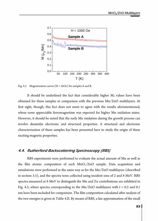
MnOx/ZnO Multilayers
83
50 100 150 200 250 300 350 4000.0
0.1
0.2
0.3
0.4
0.5
0.6
0.7
M (μ
B/M
n)
T (K)
Sample A
Sample B
H = 1000 Oe
Fig. 4.2 Magnetization curves (H = 1kOe) for samples A and B.
It should be underlined the fact that considerably higher MS values have been
obtained for these samples in comparison with the previous Mn/ZnO multilayers. At
first sight, though, this fact does not seem to agree with the results aforementioned,
where none appreciable ferromagnetism was expected for higher Mn oxidation states.
However, it should be noted that the early Mn oxidation during the growth process can
involve dissimilar electronic and structural properties. A structural and electronic
characterization of these samples has been presented here to study the origin of these
exciting magnetic properties.
4.4. Rutherford Backscattering Spectroscopy (RBS)
RBS experiments were performed to evaluate the actual amount of Mn as well as
the film atomic composition of each MnOx/ZnO sample. Data acquisition and
simulations were performed in the same way as for the Mn/ZnO multilayers (described
in section 3.5), and the spectra were collected using incident ions of 2 and 8 MeV. RBS
spectra measured at 8 MeV to distinguish the Mn and Zn contributions are exhibited in
Fig. 4.3, where spectra corresponding to the Mn/ZnO multilayers with t = 0.2 and 0.1
nm have been included for comparison. The film composition calculated after analysis of
the two energies is given in Table 4.II. By means of RBS, a fair approximation of the small

CChhaapptteerr 44
concentration of Mn in each sample is obtained. Anyway, it should be remarked that the
small % of Mn atoms obtained for samples A and B (about 2%) is near the resolution
limit order of this technique. The uncertainty in the calculated value is therefore
considerably large, what means that, for instance, small differences between the atomic compositions of sample A and B, that are in fact expected, might not be distinguished.
Fig. 4.3 (a) RBS spectra taken at energy of incident ions of 8 MeV of samples A and B. Spectra of previous t
= 0.2 and 0.1 nm samples are included for comparison.
Table 4. II. Total number of Mn atoms and sample composition obtained from simulations of RBS data.
Sample Total Mn atoms (1016 at./cm2)
Composition (%) [Mn] [Zn] [O]
A 3.2 0.02 0.49 0.49 B 3.0 0.02 0.49 0.49
t = 0.2 nm 31.5 0.13 0.34 0.53 t = 0.1 nm 26.3 0.11 0.34 0.55
350 360 370 380 390
100
200
300
400
Mn
Zn Sample A Sample B t = 0.2 nm t = 0.1 nm
Cou
nts
(arb
. uni
ts)
Channel
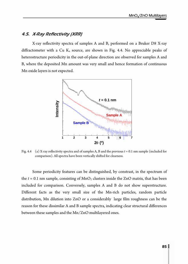
MnOx/ZnO Multilayers
85
4.5. X-Ray Reflectivity (XRR)
X-ray reflectivity spectra of samples A and B, performed on a Bruker D8 X-ray
diffractometer with a Cu Kα source, are shown in Fig. 4.4. No appreciable peaks of
heterostructure periodicity in the out-of-plane direction are observed for samples A and
B, where the deposited Mn amount was very small and hence formation of continuous
Mn oxide layers is not expected.
Fig. 4.4 (a) X-ray reflectivity spectra and of samples A, B and the previous t = 0.1 nm sample (included for
comparison). All spectra have been vertically shifted for clearness.
Some periodicity features can be distinguished, by constrast, in the spectrum of
the t = 0.1 nm sample, consisting of MnO2 clusters inside the ZnO matrix, that has been
included for comparison. Conversely, samples A and B do not show superstructure.
Different facts as the very small size of the Mn-rich particles, random particle
distribution, Mn dilution into ZnO or a considerably large film roughness can be the
reason for these dissimilar A and B sample spectra, indicating clear structural differences
between these samples and the Mn/ZnO multilayered ones.
1 2 3 4 5 6 7
Inte
nsity
2θ (º)
t = 0.1 nm
Sample B
Sample A

CChhaapptteerr 44
4.6. X-Ray Diffraction (XRD)
Diffraction measurements on these samples were carried out in a standard
laboratory diffractometer by using the Kα radiation line of Cu in θ-2θ configuration.
XRD spectra of samples A and B and the former t = 0.1 nm sample are shown in Fig. 4.5.
The (002) peak corresponding to the hexagonal wurtzite-ZnO (W-ZnO) crystal
structure can be clearly observed for samples A and B, which exhibit very similar XRD
diffractograms. Moreover, their (002) peak intensities are considerably high compared to
the t = 0.1 nm sample, which has approximately the same ZnO content, showing higher
texturation degree. Hints of a small (101) W-ZnO peak, close to 36.3º, can be also
noticed in the spectra. No additional phases are detected by this first XRD
characterization.
Fig. 4.5 X-ray diffractograms of samples A, B, where the (002)-ZnO and (400)-Sisubst peaks, at 2θ about 34º
and 69º, respectively, can be observed. The spectrum of the t = 0.1 nm sample (from the former Mn/ZnO multilayer series) has been included for comparison.
In order to obtain more structural information, X-ray diffraction experiments were
carried out in a six-circle diffractometer especially designed for thin film characterization
with λ = 0.8857 Å, at the Spanish CRG beamline (Spline, BM25, branch B) of the
European Synchrotron Radiation Facility (ESRF), in Grenoble.
20 30 40 50 60 70 80
Inte
nsity
(Arb
. Uni
ts)
2θ (º)
t = 0.1 nm
Sample A
Sample B
(002)

MnOx/ZnO Multilayers
87
Grazing incidence (ω=0.75º) and θ-2θ X-ray diffraction spectra of sample A and a
ZnO sputtered film under the same experimental conditions, included for comparison,
are depicted in Fig. 4.6. Similar grazing incidence spectra are observed for both films,
being in agreement with the ZnO reference, included in Fig. 4.6(a). Regarding the θ-2θ
scan (Fig. 4.6(b)), it can be observed that position of the (002) wurtzite ZnO peak of
sample A is in agreement with the ZnO reference, showing that there is not any
noticeable shift respect to pure W-ZnO. However, slight differences between sample A
and the ZnO film crystalline quality can be noticed. Table 4.III summarizes the size of
the ZnO wurtzite nanocrystalline grains along the out-of-plane direction obtained for
different samples by using the Scherrer formula.
Fig. 4.6 (a) Grazing incidence (ω = 0.75º) X-ray diffraction of sample A and a 70 nm sputtered ZnO film.
(b) θ-2θ X-ray diffraction of the same samples.
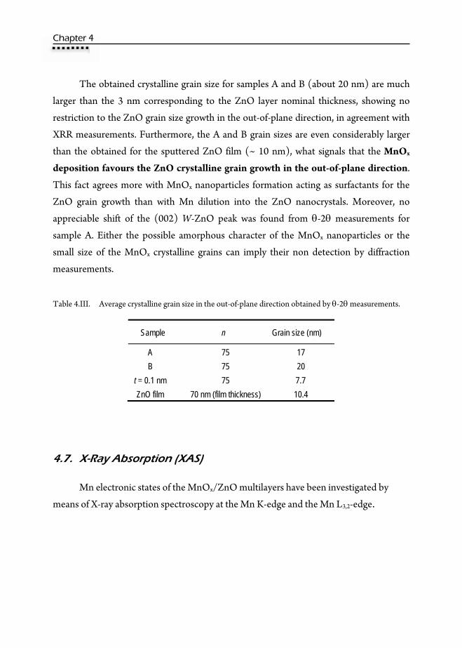
CChhaapptteerr 44
The obtained crystalline grain size for samples A and B (about 20 nm) are much
larger than the 3 nm corresponding to the ZnO layer nominal thickness, showing no
restriction to the ZnO grain size growth in the out-of-plane direction, in agreement with
XRR measurements. Furthermore, the A and B grain sizes are even considerably larger
than the obtained for the sputtered ZnO film (~ 10 nm), what signals that the MnOx
deposition favours the ZnO crystalline grain growth in the out-of-plane direction.
This fact agrees more with MnOx nanoparticles formation acting as surfactants for the
ZnO grain growth than with Mn dilution into the ZnO nanocrystals. Moreover, no
appreciable shift of the (002) W-ZnO peak was found from θ-2θ measurements for
sample A. Either the possible amorphous character of the MnOx nanoparticles or the
small size of the MnOx crystalline grains can imply their non detection by diffraction
measurements.
Table 4.III. Average crystalline grain size in the out-of-plane direction obtained by θ-2θ measurements.
Sample n Grain size (nm)
A 75 17 B 75 20
t = 0.1 nm 75 7.7 ZnO film 70 nm (film thickness) 10.4
4.7. X-Ray Absorption (XAS)
Mn electronic states of the MnOx/ZnO multilayers have been investigated by
means of X-ray absorption spectroscopy at the Mn K-edge and the Mn L3,2-edge.
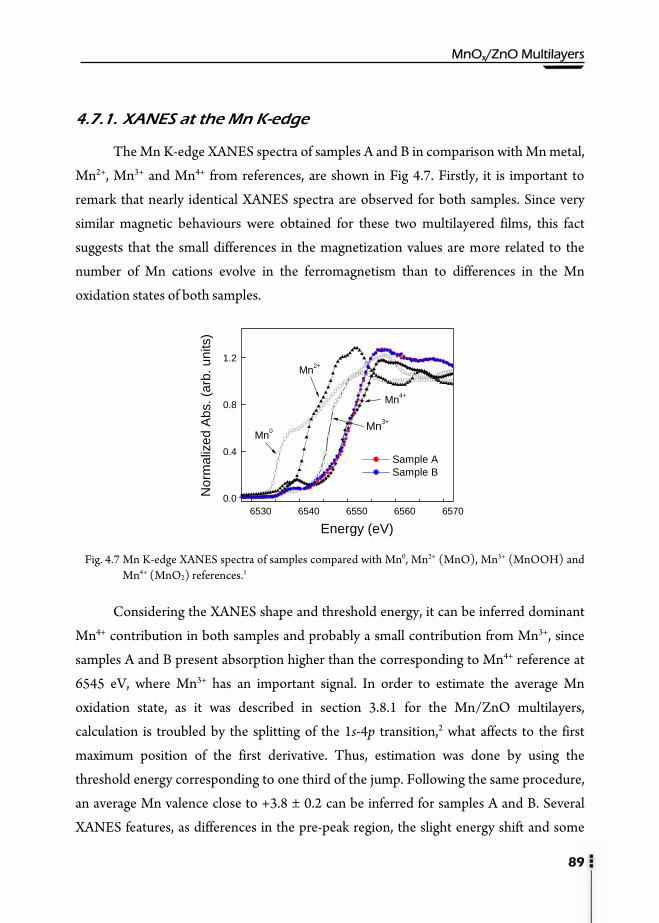
MnOx/ZnO Multilayers
89
4.7.1. XANES at the Mn K-edge
The Mn K-edge XANES spectra of samples A and B in comparison with Mn metal,
Mn2+, Mn3+ and Mn4+ from references, are shown in Fig 4.7. Firstly, it is important to
remark that nearly identical XANES spectra are observed for both samples. Since very
similar magnetic behaviours were obtained for these two multilayered films, this fact
suggests that the small differences in the magnetization values are more related to the
number of Mn cations evolve in the ferromagnetism than to differences in the Mn
oxidation states of both samples.
6530 6540 6550 6560 65700.0
0.4
0.8
1.2
Sample A Sample B
Nor
mal
ized
Abs
. (ar
b. u
nits
)
Energy (eV)
Mn2+
Mn0 Mn3+
Mn4+
Fig. 4.7 Mn K-edge XANES spectra of samples compared with Mn0, Mn2+ (MnO), Mn3+ (MnOOH) and
Mn4+ (MnO2) references.1
Considering the XANES shape and threshold energy, it can be inferred dominant
Mn4+ contribution in both samples and probably a small contribution from Mn3+, since
samples A and B present absorption higher than the corresponding to Mn4+ reference at
6545 eV, where Mn3+ has an important signal. In order to estimate the average Mn
oxidation state, as it was described in section 3.8.1 for the Mn/ZnO multilayers,
calculation is troubled by the splitting of the 1s-4p transition,2 what affects to the first
maximum position of the first derivative. Thus, estimation was done by using the
threshold energy corresponding to one third of the jump. Following the same procedure,
an average Mn valence close to +3.8 ± 0.2 can be inferred for samples A and B. Several
XANES features, as differences in the pre-peak region, the slight energy shift and some

CChhaapptteerr 44
XANES shape dissimilarities respect to Mn4+ seem to be indicative of mixed Mn
oxidation state. Nevertheless, in order to obtain more information about this fact,
additional XAS measurements have been done at the Mn L3,2-edge.
4.7.2. XAS at the Mn L3,2 –edge
The Mn L3,2 XAS structure is a fingerprint for the 3d count, giving reliable
information on the Mn oxidation state and symmetry. (Details of the Mn L3,2 XAS
spectra characteristics and calculations are described in section 2.6.2)
Figure 4.8 shows the normalized XAS spectrum of sample A measured at RT,
where the L3 and L2 step edges have been subtracted from the experimental XAS
spectrum. It can be observed that the L3 edge exhibits complex multiple absorption
peaks, what is a hint of mixed charge states in sample A. Theoretical calculations for the
Mn3+ (d4) and Mn4+ (d3) electronic configurations in Td environment3 have been
included in the figure for comparison. The multiple experimental features of the
experimental spectrum indicate that 3dn → 2p53dn+1 absorption spectrum
corresponds to a mixed Mn3+/Mn4+ ground state, as it was pointed by the Mn K-edge
XANES measurements.
640 645 650 655 660 665
Mn d4 Td
Mn d3 Td
Inte
nsity
(arb
. uni
ts)
Energy (eV)
Sample A Mn L3,2edge
Fig. 4.8 Normalized Mn L3,2 XAS spectra of sample A measured at RT. The L3 and L2 step edges have been
subtracted by two atan functions after background removal. Calculations of Mn3+ (d4) and Mn4+ (d3)
in Td crystal symmetry and appreciable crystal field (10Dq = 1-3 eV) are included for comparison.

MnOx/ZnO Multilayers
91
4.8. Thermal post-deposition annealing
With the purpose of modifying their magnetic response, thermal post-annealing of
the samples was carried out. Samples were annealed in a vacuum system furnace, firstly
evacuated up to 1 x 10⁻⁶ mbar. The thermal treatment was performed under oxygen
atmosphere of 1 x 10⁻² mbar, during two hours at 750 ºC. The XANES spectra at the Zn
K-and at the Mn K-edge as well as the obtained evolution of the magnetic properties are
given in Fig. 4.9.
The Zn K-edge XANES spectra of sample A, as-grown and after annealing, shown
in Fig 4.9(a), are nearly identical, and they do not present any significant difference in
comparison with the included ZnO spectrum. Just a nearly negligible enhance of the
signal amplitude for the annealed sample, which can be assigned to the improvement of
the ZnO crystal quality after the thermal treatment, could be inferred.
Looking at the Mn K-edge spectra of the samples, by contrast, we can found
remarkable changes in the spectra (Fig. 4.9(b)). After annealing, a clear energy threshold
shift towards lower energies is obtained. This fact evidences that, even if oxygen gas was
introduced in the vacuum furnace during all the thermal treatment, annealing leads to a
decrease of the Mn average oxidation state in the samples. Considering the spectral shape
and threshold energy, it can be inferred that after annealing, the dominant Mn4+
contribution turns into Mn3+. Comparing with the Mn3+ spectrum, there are several
spectral dissimilarities which indicate that manganese in the annealed samples is not in a
pure Mn3+ oxidation state. The coexistence of mixed Mn3+ and Mn4+ valences with
major presence of Mn3+ is pointed out by XANES. Furthermore, it is important to
remark that sample A and B exhibit extremely similar as-grown XANES spectra. After
thermal treatment, their spectral shape is considerably modified, but in the same manner
for both samples, which show again nearly identical XANES spectra, what is a clear sign
of the reproducibility of the process.
The evolution of the ferromagnetic response with the annealing treatment is
shown in Fig. 4.9(c). Although RTFM is still observed, thermal treatment of samples
involve a noticeably worsen of the ferromagnetic properties, leading to a reduction of the
CChhaapptteerr 44
magnetization of about one half. According to the XANES results for the as-grown and
annealed samples, RTFM here seems to be related mostly to Mn4+, which coexists
with Mn3+. Additional effects from annealing, as for instance improvement of
crystallinity or film texture, can modify the magnetic behaviour. However, all these facts
seem to point more towards the enhancement of the magnetic anisotropy and
consequently improve ferromagnetism, than to the outcome decrease. Nonetheless, the
reported results in this point are also controversial.4
A more detailed discussion is presented below to examine the origin of the RTFM
obtained for these MnOx/ZnO samples (A and B) in comparison with the previous
Mn/ZnO ones.
4.9. Discussion and remarks: the origin of FM in MnOx/ZnO multilayers versus the origin in the so-called Mn/ZnO multilayers.
The obtained results indicate de formation of MnO2-δ nanoparticles embedded
in W-ZnO for the two similar samples (A and B) prepared by oxidizing Zn and Mn by
sequential reactive sputtering.
XANES measurements at the Mn K-edge have indicated an average Mn oxidation state
slightly smaller than + 4 in both samples. In addition, XRD measurements have shown
that there is not any shift in the (002)-wurtzite peak of these samples with respect to the
pure W-ZnO, according to no Mn inclusion into the ZnO lattice. In fact, the big
differences between the Zn2+ and the Mn4+ ionic radii make Mn4+ diffusion into ZnO not
very likely.5 Either the amorphous character of the MnO2-δ nanoparticles or the small size
of the crystalline grains can imply their non detection by XRD.
RBS measurements have shown that the atomic composition of both samples is
approximately Mn0.02Zn0.49O0.49, confirming the small Mn relative ratio in the films. Both
the small Mn amount and the small MnO2-δ particle size agree with the XRR spectra,
which exhibited lack of heterostructure periodicity in the out-of-plane direction.
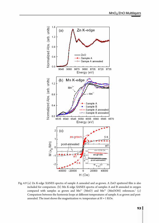
MnOx/ZnO Multilayers
93
Fig. 4.9 (a) Zn K-edge XANES spectra of sample A annealed and as-grown. A ZnO sputtered film is also
included for comparison. (b) Mn K-edge XANES spectra of samples A and B annealed in oxygen compared with samples as grown and Mn2+ (MnO) and Mn3+ (MnOOH) references.1 (c) Comparison between the hysteresis loops at different temperatures of sample A as grown and post-annealed. The inset shows the magnetization vs. temperature at H = 1 KOe.

CChhaapptteerr 44
Apart from that, it has been shown by XRD that the presence of these small
manganese oxide grains favours the ZnO crystalline grain growth in the out-of-plane
direction, increasing the ZnO grain size in this axis by a factor of 2. This fact is a sign of
the MnO2-δ-ZnO interface interaction, which might relax possible stresses appearing
during growth and allow larger ZnO grains.
Regarding the magnetic properties, ferromagnetic ordering above RT has been
found for the two similar samples. The MS values obtained here, in comparison with the
found for the Mn/ZnO samples, are significantly larger, more than one order of
magnitude. However, these results seem to completely disagree with the former ones
explained for the Mn/ZnO multilayered samples, since no appreciable ferromagnetic
order was expected for these higher Mn oxidation states. In order to resolve this apparent
discrepancy, several facts should be taken into consideration.
Firstly, the obtained magnetization values have been normalized to the total
amount of Mn in each case. However, in the case of Mn/ZnO samples, it was found that
not all the Zn-Mn-O phases contribute to ferromagnetism, being responsible just Mn in
the wurtzite phase. Therefore, the actual effective magnetizations per Mn atom in these
samples become somewhat larger.
For the MnOx/ZnO samples, though, considering the small Mn/Zn ratio (about 4
at. %) and the lack of experimental evidences of coexistence of different phases, it seems
reasonable to think that most of the MnO2-δ nanoparticles are in the same
crystallographic phase, all contributing similarly to the ferromagnetic order. In this case,
however, there is higher uncertainty in the calculation of the effective magnetization per
Mn atom that comes from the small value of the Mn atomic density obtained by RBS,
which is one order of magnitude smaller than in the Mn/ZnO samples and close to the
resolution limit. Small variations in the number of Mn atoms can lead to big differences
in the calculated magnetization per Mn atom. However, the Mn amount in the samples
cannot be much larger than the obtained by RBS.

MnOx/ZnO Multilayers
95
Nevertheless, all these facts are not enough to explain the large magnetization
values found for these samples (MS of 2 x 10⁻⁴ emu/cm2 compared to 6 x 10⁻⁵ emu/cm2,
obtained for the most ferromagnetic Mn/ZnO sample; both values are normalized to the
sample area and without normalizing to the Mn amount).
Actually, the obtained results indicate that the origin of the interaction governing
the magnetic properties of the previous Mn/ZnO films, where freshly deposited Mn with
high reactivity becomes oxidized prompted by the ZnO presence, clearly differs from the
case of intentional Mn oxidation during the growth process. Besides, the smaller grain
size of the MnO2-δ particles here enhances the effect of the surrounding ZnO.
While in the case of Mn/ZnO layers, RTFM was due to the formation of Wurtzite
Zn-O-Mn phase in a mixed W-RS oxide, it seems that in this case RTFM is not associated
with a phase but with the interface between nonferromagnetic phases.
Previous works carried out by M. A. García et al.6 and J. F. Fernández et al.7 on Mn-
Zn-O bulk samples prepared from ZnO-MnO2 mixed powders (2%MnO2-98%ZnO and
10%MnO2-90%ZnO) have shown that the presence of the ZnO around MnO2 modifies
the kinetics of MnO2 → Mn2O3 reduction and favours the coexistence of both Mn
oxidation states.
In our samples, the MnO2-δ-ZnO interaction at the interface has been evidenced
by XRD while the coexistence of Mn4+ and Mn3+ has been confirmed by Mn K-edge and
Mn L-edge XANES measurements.
The origin of the ferromagnetism here agrees with the new class of surface
magnetism proposed by M. A. García and co-workers6: double-exchange mechanism,
at the interface between two compounds containing Mn atoms in different
oxidation states. The presence of Mn3+ cations in the MnO2 is not sufficient for the
appearance of FM response. The FM is by contrast related to the coexistence of Mn3+
and Mn4+ ions at the Zn diffusion front, into the manganese oxide grains, being the
presence of Zn cations required for the double-exchange mechanism.
The explanation of the process is the following:

CChhaapptteerr 44
The double exchange mechanism is based on the fact that Mn4+ and Mn3+
separated by an O can share an electron (reducing in this way their energy) by
simultaneous transfer of an electron from one Mn atom to the O and from the O to the
other Mn atom, as illustrated in Fig 4.10, similarly to the reported in Ref. 8. Because the
spin cannot change in this transfer, a condition for this itinerancy is that both manganese
ions must be polarized. Therefore, it implies a reduction of the energy associated to
magnetic order that is responsible for ferromagnetic behaviour. Apart from the Mn4+ and
Mn3+ coexistence, particular geometry on the Mn-O-Mn bonds must be satisfied for the
interaction.
Fig. 4.10 Representation of the double exchange mechanism between Mn3+ and Mn4+
It has also been reported7 that, at higher temperatures, the stable Mn-Zn-O form is
the spinel phase (ZnxMn3-xO4), which allows the incorporation of excess Mn. As the
spinel phase progress, it has been obtained the reduction of the MS, what corroborates
that the FM response is not associated with the formation of such a phase. In our
experiments, thermal treatment of the MnO2-δ nanoparticles inside the W-ZnO
matrix showing RTFM, have also led to a marked reduction of the FM signal, what has
been related to the considerable increased of Mn3+, what would be in agreement with
these reports, according to the proposed double-exchange mechanism.
Considering the double exchange mechanism in the Mn-Zn-O system, the smaller
amount of manganese in the mixture, the larger the ferromagnetic response (to a certain
limit), since FM is increased by maximizing the interface. Taking into account the

MnOx/ZnO Multilayers
97
observed magnetic differences between the MnOx/ZnO and Mn/ZnO series, this fact
can clarify the absence of ferromagnetism in those Mn/ZnO samples consisting of MnO2
clusters inside the ZnO matrix. Both the much higher Mn/Zn relative ratio in the
Mn/ZnO samples that present MnO2 grains (about 30 at. % for the t = 0.1 nm sample)
in comparison with the MnOx/ZnO ones (about 4 at. %) and the associated smaller
effect of the neighbouring ZnO can explain the absence of ferromagnetism in that
case.
Summarizing, regarding both sample series, we have found that the ZnO presence
has a significant influence either on the deposited Mn or MnO2. On one hand,
considering the reactive sputtering process, possible oxygen excess at the surface of the
former deposited ZnO layer together with the high reactivity of the freshly deposited Mn
can imply the oxidization of the very close Mn atoms. On the other hand, the ZnO that
surrounds small and highly oxidized manganese grains seems to favour the MnO2
reduction, which usually starts at a lower temperature in the presence of Zn. In both
situations, a thermodynamically stable MnOx-ZnO state seems to be reached. Our
experimental results show that the origin of the ferromagnetism is different in both cases.
The first mechanism consists on magnetic interactions between the Mn2+ cations of a
wurtzite Zn-O-Mn phase via the carriers, while the second one is associated with the
coexistence of Mn3+ and Mn4+ that interacts via double exchange mechanism. The
different types of ferromagnetic interactions seem greatly influenced by the particular
Mn oxidation or reduction process during growth. Reduction of an initially highly
oxidized Mn phase by the surrounding ZnO effect has led to ferromagnetic order
through double exchange. By contrast, just a small paramagnetic-like signal has been
found in originally metallic Mn that highly oxidized during growth. In this former
situation, a ferromagnetic signal has only been found when the average Mn oxidation
state is close to +2, case where FM based on Mn2+ in W-ZnO phase is suggested.
Therefore, two different approaches to the study of the role of interfaces and
the relevance of the Mn oxidation state in the Mn-Zn-O system have led to two
different types of magnetism that can be possible in this system. Since these

CChhaapptteerr 44
mechanisms are not incompatible, taking both into consideration can contribute to
clarify the controversy on the ferromagnetic origin of this system.
4.10. Conclusions
In this chapter, the relevance of the Mn oxidation state in the ferromagnetic
response of the Mn-Zn-O system as well as the important role played by the ZnO-MnOx
interface region has been confirmed once more.
Nano-sized MnO2-δ grains embedded in W-ZnO (with Mn/Zn ratio of
approximately 4 at. %) have been obtained by oxidizing Zn and Mn by sequential
reactive sputtering.
The presence of these small manganese oxide grains greatly favours the ZnO
crystalline grain growth in the out-of-plane direction, what is a sign of the MnO2-δ-ZnO
interface interaction.
Ferromagnetic response over room temperature has been found for these samples,
showing MS values as large as 0.8 μB per Mn atom at RT.
Experimental results signal that the origin of the ferromagnetism in these MnO2-δ-
ZnO samples comes from the simultaneous presence of Mn3+ and Mn4+ ions that, under
the effect of the neighbouring ZnO, interact via double-exchange mechanism. The
coexistence of Mn4+ and Mn3+ has been confirmed by Mn K-edge and Mn L3,2-edge
XANES measurements.
Looking into these MnO2-δ-ZnO samples (named as MnOx/ZnO multilayers)
together with the former multilayers labelled as Mn/ZnO multilayers, it has been
evidenced that the ZnO presence has a significant influence either on the deposited Mn
or MnO2, being the origin of the ferromagnetism different in both cases.
Two different approaches to the study of the Mn-Zn-O system have led to two
different types of magnetism. One mechanism is based on magnetic interactions

MnOx/ZnO Multilayers
99
between the Mn2+ cations of a wurtzite Zn-O-Mn phase while the second one is
associated with double exchange mechanism between Mn4+ and Mn3+.
In these multilayered samples, the obtained RTFM assigned to double exchange
mechanism is nearly one order of magnitude stronger than the RTFM achieved to the
Mn-Zn-O wurtzite phase formation. Nevertheless, the two mechanisms are not
incompatible, fact that should be considered to clarify the controversy on the
ferromagnetic origin of this system.
References
1 D.A. McKeown and J.E. Post, Am. Mineral. 86, 701 (2001).
2 M. Croft, D. Sills, M. Greenblatt, C. Lee, S.-W. Cheong, K. V. Ramanujachary and D. Tran, Phys. Rev. B 55, 8726 (1997).
3 G. van der Laan and I. W. Kirkman, J. Phys.: Condens. Matter 4, 4189 (1992).
4 F. Pan, C. Song, X. J. Liu, Y. C. Yang and F. Zeng, “Ferromagnetism and possible application in spintronics of transition-metal-doped ZnO films”, Mat. Science and Engeneering R 62, 1-35 (2008).
5 M. Peiteado, A.C. Caballero and D. Makovec, J. Solid State Chem. 180, 2459 (2007).
6 M. A. García, M. L. Ruiz-González, A. Quesada, J. L. Costa-Krämer, J. F. Fernández, S. J. Khatib, A. Wennberg, A. C. Caballero, M. S. Martín-González, M. Villegas, F. Briones, J.M. González-Calbet, and A. Hernando, Phys. Rev. Lett. 94, 217206 (2005).
7 J. F. Fernández, A. C. Caballero, M. Villegas, S. J. Khatib, M. A. Bañares, J. L. G. Fierro, J. L. Costa-Kramer, E. López-Ponce, M. S. Martín-González, F. Briones, A. Quesada, M. García and A. Hernando, J. Eur. Ceram. Soc. 26, 3017 (2006).
8 A. Quesada, M. A. García, P. Crespo and A. Hernando, J. Magn. Mag. Mat. 304, 75 (2006).


101
5.1. Motivation
Differing from the type of studies carried out along Chapters 3 and 4, where
multilayered samples were prepared in order to study the role of Mn-ZnO and MnOx-
ZnO interfaces on the ferromagnetism of the Mn-Zn-O system, this chapter focuses on
the basic study dealing with Mn:ZnO in the field of DMSs, that is, preparation of actual
DMS thin film samples. In particular, the aim of this chapter is to obtain actual DMS by
preparing ZnO thin films doped with approximately 5% at. Mn (labelled as Zn0.05Mn0.95O
films), where Mn2+ cations are expected to replace Zn2+ cations in ZnO. In this case,
different gases atmospheres have been used during the sputtering process in order to
modify the magnetic properties of the prepared samples and to get further knowledge of
the nature of the expected RTFM.
Regarding the role of carrier density in ZnO-based DMSs, first theoretical
calculations predicted RTFM in n-type Co2+:ZnO while a hole-rich environment was
predicted for RTFM in Mn2+:ZnO DMSs.1,2 However, experimental results on Mn:ZnO
have been very controversial3,4 and RTFM has been also obtained in n-type Mn:ZnO
samples.5,6,7,8 Very recently, experiments performed by Z. Yang et al.9 on n-type ZnO:Mn
thin films prepared with plasma-assisted molecular-beam epitaxy using different amounts
of Ga dopant incorporation have shown evidences of electron-mediated RTFM in n-type
Mn:ZnO, contradicting the initial theory.
Whereas in general, ZnO is intrinsically n-type conducting due to shallow donors
associated with low-energy native point defects, such as oxygen vacancies (VO) and Zn
interstitials (Zni), it has been shown that nitrogen is a promising acceptor impurity for p-
type ZnO.10 However, although there is a report of experimental success in obtaining p-
CChhaapptteerr 55
Mn:ZnO Thin Films

CChhaapptteerr 55
type ZnO using a pure nitrogen source,11 it is still difficult to achieve high hole densities
due to compensation by O vacancies, NO-ZnO or NO-(N2)O complexes, even if an active
plasma N2 is used.12 Nonetheless, reduction of the n-type sample character is expected by
partial oxygen substitution by nitrogen.
On the other hand, S. Lee et al.13 have reported that the electron carrier
concentration in Zn1–xMnxO thin films prepared by RF magnetron sputtering drastically
decreases with increasing PO2, up to an Ar/O2 ratio of 1:1, while the photoluminescence
peaks related to oxygen vacancies (VO) gradually diminish, showing that the carrier
concentration can be controlled by varying PO2, as observed similarly in the host ZnO
material.
With the aim of modifying the carrier density in the Zn0.05Mn0.95O thin films,
samples have been deposited with different sputtering working gases (pure Ar, Ar/N2
and Ar/O2) under the same working pressure. In this chapter, the magnetic properties of
the prepared Zn0.05Mn0.95O films have been associated firstly, with the Mn short range
order in the lattice, and secondly, with the different gas during the deposition process.
5.2. Preparation of Mn:ZnO films
A series of Mn-ZnO thin films was prepared by DC sputtering on Si(100) and
fused quartz substrates at RT. Special attention was paid to the starting material and
different pellets were sintered from mixing ZnO and different Mn oxides to be used as
sputtering targets. The films described here were sputtered from Zn0.95Mn0.05O pellets
obtained from mixing ZnO and Mn2O3.
The Zn0.95Mn0.05O ceramic targets were sintered following this procedure:
Appropriate amounts of Mn2O3 (325 mesh, 99% ALDRICH) and ZnO (<1μ, 99.9%
ALDRICH) to obtain 5% at. of Mn were mixed and grind using acetone in an agate
mortar. The obtained powders were uniaxially pressed at 2000 N/cm2. The resulting
pellets (2.5 inch diameter) were sintered in air at 800 ºC for 6 hours. The annealing ramp
is represented in Fig. 5.1.

Mn:ZnO Thin Films
103
0 100 200 300 400 500 600 700 800 900
200
400
600
800
Tem
pera
ture
(ºC
)
time (min)
800ºC 6 hours
3ºC/min 3ºC/min
Fig. 5.1 Annealing ramp for the Zn0.95Mn0.05O ceramic target sintering.
After sintering, targets colour turned a little bit yellowish, what might be
attributed to the presence of oxygen defects. These final Zn0.95Mn0.05O ceramic targets,
very close to the 2 inch magnetron size, were used as starting bulk material for the
sputtering deposition process, described below.
The base pressure provided by the vacuum system was in the 10-7 mbar range. The
sputtering deposition was performed under a working pressure of 6.0x10⁻³ mbar with a
RF power of 30 W to obtain a deposition rate in the 2-4 nm/min range, depending on the
working gas. With the aim of modifying the carrier density, samples were deposited with
different sputtering working gases (pure Ar, Ar/N2 and Ar/O2) under the same working
pressure. The sample series description and main deposition parameters are summarized
in Table 5.I.
Additionally, some annealing treatments were performed after film growth. The
post-deposition thermal treatments were carried out inside a quartz tube previously
evacuated up to 1 x 10⁻⁶ mbar, under oxygen atmosphere flow of 1 x 10⁻² mbar during two
hours at 750 ºC. The description of the annealed samples is shown in Table 5.II.

CChhaapptteerr 55
Table 5.I Zn0.95Mn0.05O sample series summary and main deposition parameters as substrate temperature (TS), RF power, sputtering deposition time (tsputt), film thickness (Λ) and deposition rate (Δ).
target TS (ºC)
Sputtering gas (P = 6x10⁻³ mbar)
Power (W)
tsputt (min)
Λ (nm)
Δ (nm/min)
Sample label Zn0.95Mn0.05O
Zn0.95Mn0.05O 25 100% Ar 30 30 108 3.6 -Ar
Zn0.95Mn0.05O 25 83% Ar; 17% N2 30 30 102 3.4 -Ar/N2
Zn0.95Mn0.05O 25 83% Ar; 17% O2 30 30 61 2.0 -Ar/O2
Zn0.95Mn0.05O 600 83% Ar; 17% O2 30 60 42 0.7 -Ar/O2-TS=600ºC
Table 5.II Annealed Zn0.95Mn0.05O samples description: annealing temperature (TA), oxygen pressure during annealing (PO2), annealing time (tA), sample thickness after annealing and sample label.
As-grown sample Annealing conditions
Λ (nm)
Sample label Zn0.95Mn0.05O TA (ºC) PO2 (mbar) tA (h)
Zn0.95Mn0.05O-Ar 750 1x10⁻² 2 94 -Ar-750ºC-O2
Zn0.95Mn0.05O-Ar/N2 750 1x10⁻² 2 92 -Ar/N2-750ºC-O2
In addition, 1 μm thick films were grown afterwards under identical experimental
conditions (gas pressure, RF power, substrate temperature) as described above (Table
5.I), with two purposes: the increase of the XRD intensity for a better detection of
possible additional extrinsic phases and the enhancement of the XAS spectra threshold
jump intensity for a more detailed XANES study.
5.3. X-Ray Reflectivity (XRR)
X-ray reflectivity (XRR) measurements were carried out on a Bruker D8 X-ray
diffractometer with a Cu Kα source at the ICMM facilities. XRR film spectra, shown in
Fig. 5.2, reveal different deposition rates depending on the sputtering gas.

Mn:ZnO Thin Films
105
1.0 1.5 2.0 2.5
Log
Inte
nsity
(ar
b. u
nits
)
2θ (º)
Ar Ar-ann-750ºC-O2
Ar/N2
Ar/N2-ann-750ºC-O2
Ar/O2
Ar/O2-TS=600ºC
Fig. 5.2 XRR spectra of the Zn0.95Mn0.05O films prepared using different gas atmospheres and after thermal
treatments in oxygen atmosphere.
The obtained film thickness and deposition rates for the as-grown samples are
given in Table 5.I. It can be observed that the sputtering gas efficiency decreases from
samples prepared with Ar, Ar/N2 to Ar/O2. While deposition rates using 100% Ar and
Ar/N2(17%) are very similar (3.6 and 3.4 nm/min, respectively), a remarkably
diminution of about 45% is obtained for Ar/O2(17%), becoming 2.0 nm/min.
The sputtering yield (S = number ejected atoms / number incident atoms)
depends basically on the target material (binding energy, mass of atoms), the sputtering
gas (mass of atoms, increasing S for heavier gasses and incident energy, increasing S for
higher energies) and the geometry (most efficient 20-30 degrees from glancing), as it was
explained in section 2.1. Therefore, under the same geometry and the same target
material, it is expected that S increases as the mass of the gas atoms becomes bigger. The
atomic mass of argon is 40, while the oxygen and nitrogen molecular mass are 32 and 28,
respectively.
For the same working pressure, the deposition rate, which is directly related to S,
increases with S. The larger sputtering yield for Ar may explain the small difference found

CChhaapptteerr 55
in the deposition rates using 100% Ar and Ar/N2(17%), 3.6 and 3.4 nm/min,
respectively. Conversely, the noticeable diminution in the deposition rate when
introducing oxygen, Ar/O2(17%), can be related to the higher reactivity of the oxygen
gas and the expected chemical reactions on substrate and target, which can substantially
modify the process dynamics.
Additionally, if the deposition process takes place under higher substrate
temperature (TS = 600ºC, instead of 25ºC, see Table 5.I) without modifying other
growth parameters (same gas atmosphere, Ar/O2 (17%)), the deposition rate is
drastically modified, decreasing to 0.7 nm/min (∼80% diminution). This seems to be
related to the diminution of the sticking coefficient as the substrate temperature is
elevated. Furthermore, the observed increased amplitude in the XRR spectrum of
Zn0.95Mn0.05O-TS=600ºC sample in comparison with the others (Fig. 5.2) might be
associated with a decrease of the film surface roughness for higher substrate temperature,
probably due to the increase of the adatom mobility.
On the other hand, post-deposition annealing at 750ºC in oxygen atmosphere of
the Ar and Ar/N2− prepared samples, summarized in Table 5.II also leads to a slight
reduction of the film thickness (∼10%), what can be interpreted as a sample compaction,
increasing the film density.
5.4. Rutherford Backscattering Spectroscopy (RBS)
Rutherford backscattering spectroscopy (RBS) experiments were carried out in
order to determine the actual Mn content inside the films. Fig. 5.3 shows the RBS spectra
of several samples, what allows to compare the relative Mn concentration among them. It
is observed a nearly constant Mn/Zn ratio independently of the preparation conditions,
with values a bit larger but very similar to the nominal ones in the target; the
experimental Mn/Zn ratio obtained after fitting, close to 6%, is displayed in the
legend of Fig. 5.3.

Mn:ZnO Thin Films
107
100 200 300 400 500
Cou
nts
(arb
. uni
ts)
5.8%
6.7%
6.1%
Mn/Zn ratio
Ar/O2
Ar/N2-ann-750ºC-O2
Channel
Zn
MnSi substrate
OAr
Ar/N2
Fig. 5.3 RBS spectra of several Zn0.95Mn0.05O thin films. The Mn/Zn ratio is given for each sample.
5.5. X-Ray Diffraction (XRD)
Diffraction measurements on the sample series were carried out in a standard
Bruker D8 X-ray diffractometer by using the Kα radiation line of Cu. Fig. 5.4 shows X-ray
diffraction spectra corresponding to several Zn0.95Mn0.05O films and a ZnO film
deposited from a ZnO target under similar pressure and RF power using pure Ar gas (all
of them in the 100 nm thick range). The prepared films show just the (002) peak
corresponding to the typical wurtzite ZnO crystallographic structure, showing different
texturation degrees. No additional extrinsic phases are detected by XRD, even for
identically prepared 1 μm thick films. However, (100) and (101)-ZnO peaks were
additionally identified in the XRD spectrum of the Ar/O2−prepared 1 μm sample,
evidencing lower texture in the Ar/O2-sample.
Results from XRD analysis are given in Table 5.III. The position of the observed
(002)-ZnO diffraction peaks for the as-grown samples under different atmospheres (Ar,
Ar/N2 and Ar/O2) is approximately the same (2θ ∼ 33.7º), which is smaller than the
expected (002)-ZnO peak position in wurtzite structure (2θ = 34.4º). A close 2θ value

CChhaapptteerr 55
(as well as an increase of the crystalline grain size) is only obtained after post-deposition
annealing in oxygen.
31 32 33 34 35 36 37
Inte
nsity
(arb
. uni
ts)
2θ (º)
x3
(002)-ZnO
ZnO film
Ar/N2Ar/O2
Ar-ann-750ºC-O2
Ar
Fig. 5.4 X-ray diffraction patterns of the Zn0.95Mn0.05O samples. Table 5.III Zn0.95Mn0.05O XRD results summary: (002)-ZnO peak position (2θ) and full width at half
maximum (FWHM) from Gaussian fits and the corresponding grain size in the out-of-plane direction obtained by the Scherrer equation.
Sample XRD (002)-ZnO
2θ (º) FWHM (º) grain size (nm)
ZnO-Ar 33.7 0.56 14.8
Ar 33.7 0.47 17.7
Ar-ann-750ºC-O2 34.4 0.28 29.7
Ar/N2 33.75 0.40 20.8
Ar/O2 33.9 0.44 18.9
Besides, it should be noticed that the ZnO film deposited with pure Ar gas (ZnO-
Ar) under similar conditions presents (002)-ZnO peak also at 33.7º, differing from
expected position. All these facts suggest the presence of tensile stresses in the as-grown

Mn:ZnO Thin Films
109
films, both in ZnO and Zn0.95Mn0.05O films. Sample annealing at 750ºC in oxygen
atmosphere would lead to stress relaxation, what agrees with 2θ = 34.4º obtained for the
Ar-ann-750ºC-O2 sample, coinciding with the stress-free powder value.
Additionally it can be observed that the Ar/O2− prepared sample presents a small
shift of the (002) peak to higher angles (2θ = 33.9º) compared to the ZnO−Ar film (2θ
= 33.7º). Just under the hypothesis that stress affects similarly all the as-grown Mn:ZnO
films because of their similar thickness (∼100 nm), the observed shift might be
associated with the presence of oxygen vacancies in the ZnO−Ar film, as well as in the
Zn0.95Mn0.05O films prepared with Ar (2θ = 33.7º) and with Ar/N2 (2θ = 33.75º), since
the presence of oxygen vacancies in the ZnO lattice involve a shift to smaller angles.14
Anyway, it should be keep in mind that this is just a lucubration only valid under the
considered assumptions (similar tensions in the films and Mn occupying the same lattice
position in the compared as-grown Mn:ZnO films).
The calculated (002)-ZnO crystalline grain sizes in the out-of-plane direction by
using the Scherrer formula (shown in Table 5.III) range between 15 and 30 nm
approximately. The obtained sizes for the Zn0.95Mn0.05O films are larger than for the
ZnO−Ar film. While crystalline grain sizes close to 20 nm have been found for the Ar,
Ar/N2 and Ar/O2− as grown Zn0.95Mn0.05O samples, approximately 15 nm of average size
has obtained for the ZnO−Ar film. As well, post-deposition annealing of the Ar/N2
sample in oxygen atmosphere leads to an noticeable increase of the crystalline grain size
(from 21 to 30 nm).
5.6. Magnetic properties
The magnetic characterization, performed with a SQUID magnetometer (MPMS-
7T from Quantum Design) is shown in Fig. 5.5. Magnetization per manganese atom has
been calculated, after subtracting the diamagnetic Si contribution, taking into account
the precise amount of Mn obtained by RBS. It should be noted here that the selected
samples have similar thickness and hence normalization to film volume or area gives
similar results.
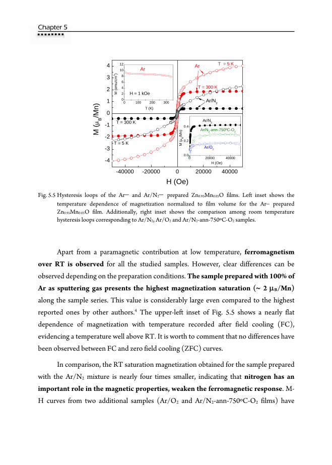
CChhaapptteerr 55
-40000 -20000 0 20000 40000
-4
-3
-2
-1
0
1
2
3
4
0 100 200 3000
2
4
6
8
10
12
0 20000 400000.0
0.2
0.4
Ar
H = 1 kOe
Ar/O2
Ar/N2-ann-750ºC-O2
Ar/N2
M (μ
B/Mn)
H (Oe)
Ar T = 5 K
T = 300 K
T = 300 K
T = 5 K
M (e
mu/
cm3 )
T (K)
M (μ
B/M
n)
H (Oe)
Ar/N2
Fig. 5.5 Hysteresis loops of the Ar− and Ar/N2− prepared Zn0.95Mn0.05O films. Left inset shows the
temperature dependence of magnetization normalized to film volume for the Ar− prepared Zn0.95Mn0.05O film. Additionally, right inset shows the comparison among room temperature hysteresis loops corresponding to Ar/N2, Ar/O2 and Ar/N2-ann-750ºC-O2 samples.
Apart from a paramagnetic contribution at low temperature, ferromagnetism
over RT is observed for all the studied samples. However, clear differences can be
observed depending on the preparation conditions. The sample prepared with 100% of
Ar as sputtering gas presents the highest magnetization saturation (∼ 2 μB/Mn)
along the sample series. This value is considerably large even compared to the highest
reported ones by other authors.4 The upper-left inset of Fig. 5.5 shows a nearly flat
dependence of magnetization with temperature recorded after field cooling (FC),
evidencing a temperature well above RT. It is worth to comment that no differences have
been observed between FC and zero field cooling (ZFC) curves.
In comparison, the RT saturation magnetization obtained for the sample prepared
with the Ar/N2 mixture is nearly four times smaller, indicating that nitrogen has an
important role in the magnetic properties, weaken the ferromagnetic response. M-
H curves from two additional samples (Ar/O2 and Ar/N2-ann-750ºC-O2 films) have

Mn:ZnO Thin Films
111
been included in the bottom-right inset of Fig. 5.5, in comparison with the Ar/N2− prepared sample.
It can be observed that, although both of them exhibit a weak ferromagnetic signal
at RT, saturation magnetization values in this case are considerably much lower,
corresponding the smallest signal to the Ar/O2− prepared sample. In addition, no
appreciable FM response was found for the sample prepared with Ar/O2 flow at higher
substrate temperature (Ar/O2-TS=600 ºC sample).
Regarding the magnetic characterization of these samples, a strong dependence
of the ferromagnetic response in terms of the sputtering gasses and deposition
temperature conditions has been revealed.
5.7. X-Ray Absorption Near-Edge Structure (XANES)
As we have emphasized along this work, the local order around Mn becomes of
fundamental importance in Mn-Zn-O system studies. For that purpose, we have
performed XAS experiments at the Mn K-edge. XANES spectra were measured in
fluorescence yield detection mode at the Spanish CRG beamline (SpLine, BM25) of the
ESRF. A Mn foil and several manganese oxides were also measured to be used as
references. For these experiments, we used additional 1 μm thick films which were grown
under identical experimental conditions as the 100 nm ones. The aim was to enhance the
intensity of the collected XAS threshold jump to be able to fulfil a more thorough
XANES study.
Fig. 5.6(a) shows XANES spectra corresponding to 1 μm thick films prepared
with Ar, Ar/N2 and Ar/O2 sputtering gases. Considering the previous XANES analysis
reported along this work (sections 3.8.1 and 4.7.1), the obtained threshold energy shift
with respect to metal Mn in the films prepared with Ar and Ar/N2 gases indicates
that manganese appears mostly in the Mn2+ oxidation state. By contrast, manganese
presents a higher oxidation state (near Mn4+) when preparing under Ar/O2 atmosphere.
Details of the obtained threshold shift can be observed in Fig. 5.7, which shows a zoom of

CChhaapptteerr 55
the low energy region of the XANES spectra of these samples as well as the Ar-ann-
750ºC-O2 film, compared to a Mn metal foil.
6545 6580 6615 6650 6540 6560 6580
Exp. Mn in W-ZnO
Exp. Mn in RS-ZnO
Nor
mal
ized
Abs
orpt
ion
(arb
. uni
ts)
Energy (eV)
Ar
Ar/N2
Ar/O2
(a)
MnZn+ VZn
MnZn+ VO
MnZn
Ar/N2
Energy (eV)
Ar
(b)
Fig. 5.6 XANES spectra of Ar, Ar/N2 and Ar/O2− prepared Zn0.95Mn0.05O films firstly compared to
experimental data reported in Ref. 15 for Mn in rock-salt (RS) and in wurtzite (W) structures. (b) More detailed comparison of the Zn0.95Mn0.05O-Ar and Ar/N2 XANES spectra with calculations reported in Ref. 16 for Mn substituting Zn in stoichiometric W structure (MnZn), W with oxygen vacancies (MnZn+VO), and W with zinc vacancies (MnZn+VZn).
6530 6540 6550 6560 6570
Energy (eV)
Ar-ann-750ºC-O2
Nor
mal
ized
Abs
orpt
ion
ArAr/N2
Ar/O2
Mn-foil
Fig. 5.7 XANES spectra of the Ar, Ar/N2, Ar/O2 and Ar/N2-ann-750ºC-O2 Zn0.95Mn0.05O films in
comparison with a Mn metal foil.
Mn:ZnO Thin Films
113
It is worth to comment that the observed shift within the series (between Ar/N2,
Ar samples and the Ar/O2 one) seems quite independent of the manganese oxide used in
the target preparation, since similar results have been found for samples sputtered from
targets sintered from ZnO-MnO (see additional information at the end of this chapter).
It can be observed a small difference between the Ar− and the Ar/N2− prepared
sample spectra (Fig. 5.7) that may be described mainly by a steeper slope in the
absorption jump shape of the corresponding Ar/N2− prepared sample spectra. This
feature could be explained by a more narrow distribution of Mn2+ environments in the
Ar-prepared sample. Slightly different Mn2+ sites can give rise to different threshold
energies and consequently, broader distributions can imply less steep jump edges,
showing more gradual slopes in the normalized XANES spectra. On the other hand, the
fact that the spectrum of the Ar/N2− prepared sample is slightly shifted to smaller
energies (see Fig 5.7, jump region) indicates a small decrease in the Mn oxidation state,
which is actually the first hint pointing towards the fact that nitrogen has entered in the
lattice. O2- substitution by N3- would entail longer distances for the Mn-(O/N) shell and
consequently, smaller Mn formal oxidation state.
For the sample grown with Ar/O2 atmosphere, it appears that high oxygen
reactivity during deposition process favours the stabilization of a highly oxidized
manganese phase (and likely, also the diminution of the oxygen vacancies in the ZnO).
The small ionic radius of Mn4+ in addition to the considerable charge mismatch, makes
rather unfeasible the substitution of Zn2+ by Mn4+ in the ZnO lattice. Nevertheless,
XANES results are compatible with the presence of minor Mn2+ and Mn3+ contributions.
For the thin films grown with Ar and Ar/N2 gases, with Mn oxidation states close
to +2, based on a direct comparison with reported experimental spectra of CVD
prepared Zn0.95Mn0.05O samples15 (shown Fig. 5.6(a)) and according to Mn/ZnO
multilayers (section 3.9), it can be deduced that Mn2+ substitutes Zn2+ in the wurtzite
structure. In addition, by comparison of the XANES spectra of these samples with other
XANES studies carried out on Mn/ZnO multilayers (section 3.8.1) and Mn/Si3N4
multilayers (section 6.8.1), the presence of appreciable extrinsic phases, as MnO or even
Mn3N2, can be discarded.

CChhaapptteerr 55
Besides, a more detailed study of XANES structure of these two films allows to
characterize the Mn environment more precisely. Yan et al.16 have performed
calculations of XANES spectra for different environments of Mn2+ replacing Zn2+ in
wurtzite ZnO where vacancies or interstitials are considered. In fact, the substitution of
Zn by Mn gives slightly different spectra in three interesting cases: a stoichiometric
crystal (MnZn), a crystal with additional oxygen vacancies (MnZn+VO) and with
additional zinc vacancies (MnZn+VZn). Fig. 5.6(b) shows the comparison between the
Ar− and Ar/N2− prepared films with the calculated spectra. It can be observed that the
corresponding MnZn+VO calculated spectrum presents a characteristic feature in the
middle of the jump (marked with an arrow in Fig. 5.6(b)), which also appears in the two
studied sample spectra. By comparison, it can be noted that films prepared by
sputtering with Ar and Ar/N2 are compatible with appreciable amount of oxygen
vacancies and consequently, both samples are expected to show n-type conduction.
Summarizing, XANES results indicate that, for the Ar/O2− prepared sample as
well as for the oxygen-annealed films, manganese is mostly in a high oxidation state and
almost certainly placed out of the ZnO wurtzite structure. However, the existence of
additional minor Mn2+ and Mn3+ contributions could be expected, especially for the Ar-
ann-750ºC-O2 sample, with smaller average Mn oxidation state. This would explain the
weak ferromagnetic signal observed for the Ar/N2-ann-750ºC-O2 and for the Ar/O2− prepared samples, being smaller for the Ar/O2 one, as expected.
Conversely, XANES spectra corresponding to the films prepared with Ar and
Ar/N2 gases (oxygen deficient atmospheres) indicate that the majority Mn2+ are placed
in the cation sites of an oxygen defective wurtzite structure. Moreover, it seems that,
when N2 is introduced in the sputtering gas, nitrogen has entered in the lattice because
Mn2+ presents a slightly smaller K-edge threshold energy. Since nitrogen would act as an
acceptor impurity here, this would imply a reduction of the n-type character and
therefore, a variation of the carrier density would be expected for the Ar− and Ar/N2− prepared samples, being the Zn0.95Mn0.05O-Ar sample the richest one in electron carriers
between both. Regarding the magnetic properties, the highest saturation magnetization

Mn:ZnO Thin Films
115
has been found for the Zn0.95Mn0.05O-Ar sample, diminishing significantly the
ferromagnetic response when using Ar/N2 gases.
5.8. UV-VIS Absorption
Optical absorption measurements were carried out in order to obtain additional
information about the above supposition, before a direct evidence of the charge carrier
variation could be checked by transport measurements.
The visible - ultraviolet optical absorption of the films deposited on fused quartz
was measured with a Cary 4000 UV-Vis spectrophotometer in the 190-900 nm range.
Fig. 5.8 shows the optical absorption coefficient as a function of wavelength of the same
studied Zn0.95Mn0.05O films (about 100 nm thick) prepared on fused silica substrates to
be measured by transmission mode. A ZnO film prepared by sputtering from a pure ZnO
target with Ar gas is presented also for comparison. An estimation of the gap energy of
this ZnO film gives a value of 3.28 eV, in agreement with reported values. Additionally,
the excitonic character of the optical absorption edge can be clearly observed by the
feature at 352 nm in this undoped sample.17
200 300 400 500 600 700 800 900
350 400 450
Abso
rptio
n C
oefic
ient
(cm
-1)
Wavelength (nm)
Ar
ZnO
Ar/O2
Ar/N2
Zn0.95Mn0.05O sputtered films
Ar
ZnOAr/O2
Ar/N2
Fig. 5.8 Optical absorption coefficient of the studied samples.
CChhaapptteerr 55
Both, the Ar− and Ar/N2− prepared Mn:ZnO films show a slightly shifted
absorption edge respect to the ZnO film. Moreover, the noticeable reduction of the
excitonic feature has been related to the presence of Mn2+ in Zn1-xMnxO due to the
increase of disorder and subsequent lattice distortion.17 A more detailed study of the
optical edge (inset of Fig. 5.8) shows that Ar/N2− prepared films have a slightly larger
absorption coefficient in the 370 - 420 nm range, in agreement with the reported by Gu
et al.14 This increment might be due to the presence of nitrogen in the lattice structure,
providing additional levels in the gap. Therefore, optical measurements agree with the
inclusion of nitrogen in the wurtzite structure.
On the other hand, the Ar/O2− prepared Mn:ZnO film presents a higher
absorption from 800 nm, being in agreement with the presence of MnO2, as it has been
reported in MnO2/TiO2 nanocomposites.18
Taking into account UV-Vis characterization together with X-ray diffraction and
XANES measurements, results point towards the presence of Mn2+ in the wurtzite ZnO
lattice for Zn0.95Mn0.05O-Ar and Zn0.95Mn0.05O-Ar/N2 films, both of them with similar
amount of oxygen vacancies. The presence of intrinsic oxygen vacancies in ZnO confers
samples n-type character but as nitrogen acts as an acceptor impurity in the ZnO lattice,
substitution of O2− by N3− entails a reduction of the ZnO electron density. Therefore,
results suggest a variation of the electron carrier density of these Zn0.95Mn0.05O n-
type films where mostly Mn2+ cations substitute Zn2+ in the W-ZnO structure. Since
the highest ferromagnetic signal within the series has been found for the Zn0.95Mn0.05O-
Ar sample (with higher expected n-type carrier density) and it becomes significantly
reduced for the Zn0.95Mn0.05O-Ar/N2 film (with smaller one) these results suggest the
existence of electron mediated RTFM in Mn:ZnO films. Additional electrical
measurements are planned to prove the proposed association.
For the Ar/O2− prepared sample, XRD, XANES and optical measurements
suggest the formation of a highly oxidized manganese phase (MnO2-δ-type) coexisting
with W-ZnO structure. However, extra Mn2+ and Mn3+ minor contributions could be
expected for this sample as well as for the oxygen-annealed films (with smaller Mn

Mn:ZnO Thin Films
117
oxidation state). This might explain the small ferromagnetic signal observed for both the
Ar/N2-ann-750ºC-O2 and the Ar/O2−prepared samples, being smaller for the Ar/O2
one, what seems consistent regarding its higher average Mn oxidation state.
5.9. Conclusions
Room temperature ferromagnetism has been obtained in Mn:ZnO films prepared
by sputtering from a Zn0.95Mn0.05O target.
A strong variation of the ferromagnetic response has been found by modifying the
working gas type (Ar, Ar/O2, Ar/N2) in films prepared from the same Zn0.95Mn0.05O
target under the same sputtering working pressure.
The highest saturation magnetization values have been obtained for the Ar− and
Ar/N2− prepared Mn:ZnO films (about 2 and 0.5 μB/Mn at room temperature,
respectively), being the samples where it has been found that there is mostly Mn2+
located in the ZnO wurtzite structure.
Both the film preparation in oxygen atmosphere (Ar/O2) and the annealing
treatments after deposition in oxygen flow lead to highly oxidized Mn, close to Mn4+. The
oxygen effect is a significant reduction of the ferromagnetic signal.
X-ray diffraction, XANES and optical absorption characterizations point towards
the existence of nitrogen in the wurtzite lattice for the Ar− and the Ar/N2− prepared
Zn0.95Mn0.05O films, both of them with similar amount of oxygen vacancies. This
indicates that the two samples present n-type character, and that the electron density in
the Ar− prepared film is higher than in the Ar/N2− one. The observed difference in the
magnetic properties can be therefore related to different carrier density, being in
agreement with room temperature ferromagnetic ordering in n-type Mn:ZnO mediated
by electron carriers.
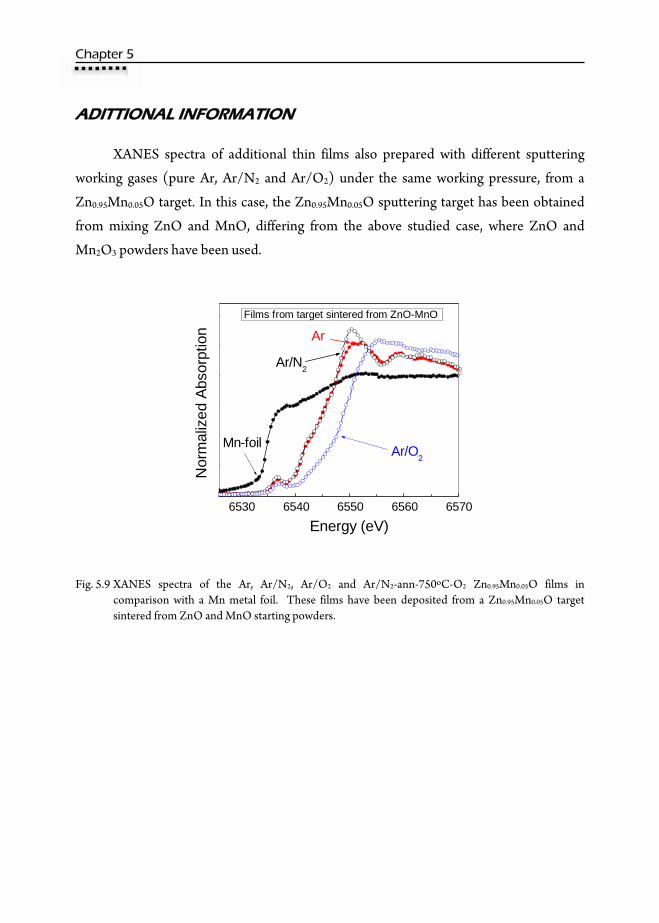
CChhaapptteerr 55
ADITTIONAL INFORMATION
XANES spectra of additional thin films also prepared with different sputtering
working gases (pure Ar, Ar/N2 and Ar/O2) under the same working pressure, from a
Zn0.95Mn0.05O target. In this case, the Zn0.95Mn0.05O sputtering target has been obtained
from mixing ZnO and MnO, differing from the above studied case, where ZnO and
Mn2O3 powders have been used.
6530 6540 6550 6560 6570
Energy (eV)
Nor
mal
ized
Abs
orpt
ion
Ar
Ar/N2
Ar/O2
Mn-foil
Films from target sintered from ZnO-MnO
Fig. 5.9 XANES spectra of the Ar, Ar/N2, Ar/O2 and Ar/N2-ann-750ºC-O2 Zn0.95Mn0.05O films in comparison with a Mn metal foil. These films have been deposited from a Zn0.95Mn0.05O target sintered from ZnO and MnO starting powders.

Mn:ZnO Thin Films
119
References
1 T. Dietl, H. Ohno, F. Matsukura, J. Cubert, and D. Ferrand, Science 287, 1019 (2000).
2 K. Sato and H. Katayama-Yoshida, Semicond. Sci. Technol. 17, 367 (2002).
3 C. Liu, F. Yun, H. Morkoc, “Ferromagnetism of ZnO and GaN: A Review”, J. Mat. Science: Materials in Electronics 16, 555 (2005).
4 F. Pan, C. Song, X. J. Liu, Y. C. Yang, F. Zeng, “Ferromagnetism and possible application in spintronics of transition-metal-doped ZnO films”, Mat. Science and Engineering R 62 1-35 (2008).
5 P. Sharma, A. Gupta, K. V. Rao, Frank J. Owens, R. Sharma, R. Ahuja, J. M. Osorio Guillen, B. Johansson, and G. A. Gehring, Nat. Mater. 2, 673 (2003).
6 Y. W. Heo, M. P. Ivill, K. Ip, D. P. Norton, S. J. Pearton, J. G. Kelly, R. Rairigh, A. F. Hebard, and T. Steiner, Appl. Phys. Lett. 84, 2292 (2004).
7 S. W. Jung, S. J. An, G. G. Yi, C. U. Jung, S. I. Le and S. Cho, Appl Phys Lett 80, 4561 (2002).
8 Y. M. Kim, M. Yoon, I. W. Park, Y. J. Park, and J. H. Lyou, Solid State Commun. 124, 175 (2004).
9 Z. Yang, J. L. Liu, M. Biasini, W. P. Beyermann, Apl. Phys. Lett. 92, 042111 (2008).
10 Q. Xu, H. Schmidt, L. Hartmann, H. Hochmuth, M. Lorentz, A. Setzer, P. Esquinazi, C. Meinecke, M. Grundmann, Apl. Phys. Lett. 91, 092503 (2007).
11 A. Tsukazaki, A. Ohtomo, T. Onuma, M. Ohtani, T. Makino, M. Sumiya, K. Ohtani, S. F. Chichibu, S. Fuke, Y. Segawa, , H. Ohno, H. Koinuma, and M. Kawasaki, Nat. Mat. 4, 42 (2005).
12 E. C. Lee, Y. S. Kim, Y. G. Jin, and K. J. Chang, Phys. Rev. B 64, 85120 (2001).
13 S. Lee, H. S. Lee, S. J. Hwang, Y. Shon, D. Young, Y. Kim and E. K. Kim, J. Cryst. growth 286, 223 (2006).
14 Z. Gu et al. Appl. Phys. Lett., 88, 082111 (2006).
15 J. Pellicer-Porres, A. Segura, J. F. Sánchez-Royo, J. A. Sans, J. P. Itié, A. M. Flank, P. Lagarde, and A. Polian, Appl. Phys. Lett. 89, 231904 (2006).
16 W. Yan, Z. Sun, Q. Liu, Z. Pan, J. Wang, S. Wei, D. Wang, Y. Zhou, and X. Xhang, Appl. Phys. Lett., 91, 062113 (2007).
17 K. J. Kim, Y.R. Park, J. Appl. Phys., 94, 867 (2003).
18 M. Xue, L. Huang, J. Q. Wang, Y. Wang, L. Gao, J. H. Zhu, Z. G. Zou, Nanotechnology, 19, 185604 (2008).


121
Annealing can have a great effect on the magnetization of TM-doped ZnO, largely
because it can modify the microstructure and local structure of samples. For instance, the
post-deposition annealing treatment may lead to a more even distribution of
substitutional Mn2+ and minimize antiferromagnetic coupling in Zn1-xMnxO thin films.1
Regarding ZnO defects, annealing in vacuum or in a reducing atmosphere might
enhance FM of these samples due to introduction of VO and ZnO defects, which have
been claimed of great importance in the RTFM of TM-doped ZnO. The formation of
this type of intrinsic defects is evolved to FM since electrons locally trapped by VO or ZnO
can occupy an orbital overlapping with the d shells of the TM neighbours to form a
bound magnetic polaron (BMP), recently related to intrinsic RTFM.2 Similarly,
annealing of samples in oxidation atmospheres can lead to a decrease in VO
concentration, with a large detrimental effect on FM.
However, experimental results in the DMS field are diverse and highly dependent
on sample preparation. Especially, the thermodynamics in Zn1-xMnxO thin films has not
been clarified yet; thus it is difficult to understand the thermodynamic behaviour of the
components, the magnetic ions, and the carriers for Zn1-xMnxO samples.
V. K. Sharma et at.3 investigated thermal treatments of non-homogeneous Zn1-
xMnxO bulk polycrystalline samples with x ranging from 0.02 to 0.25, where the
magnetization increases as the Mn content increases. They found that annealing in
hydrogenated argon (oxygen-deficient atmosphere) further enhances ferromagnetism,
whereas annealing in air (oxygen-rich atmosphere) deteriorates the ferromagnetic signal.
By contrast, B. Babić-Stojić et al.4 observed RTFM in non-homogeneous Mn-Zn-
O bulk polycrystalline samples with 10% of Mn that were thermally treated at 400 and
AAppppeennddiixx AA
Effect of Thermal Treatments and Substrate Temperature on Mn/ZnO Multilayers

AAppppeennddiixx AA
500ºC for 12 h in air. They suggested that RTFM could arise from interactions between
the Mn2+ ions and p-type defects incorporated in the ZnO crystal lattice during the
thermal treatment.
E. Chikoidze et al.5 reported that, contrary to pure ZnO films, Mn-Zn-O alloy is
highly unstable under annealing in O2, starting from temperatures as low as 300ºC. They
found that the oxygen annealing modifies the mean cation-cation distance, and the Mn2+
distribution without formation of any ferromagnetic phase.
Conversely, the ferromagnetic properties of Zn0.93Mn0.07O films were dramatically
improved after rapid thermal annealing at 900ºC in nitrogen atmosphere (S. Lee et al.6).
Their results suggest that FM of Mn-Zn-O films can be improved by modifying the
crystal magnetic anisotropy through post-growth thermal treatments.
Y. W. Heo et al.7 studied the effect of post deposition annealing on the
ferromagnetic properties of Mn implanted ZnO film deposited on Al2O3 at 400ºC.
Samples were annealed in the PLD chamber at temperatures ranging from 425 to 600°C
in O2 ambient (~10-1 mbar) for 60 min. A significant enhancement in the magnetization
after annealing at 600ºC was observed, which was attributed to the improvement of
crystalline quality.
On the other hand, substrate temperature can importantly affect the
magnetization of TM-ZnO films since it can also modify structural defects. For instance,
P. Sharma et al.8 reported that Mn-Zn-O films prepared at low processing temperature
exhibited RTFM, whereas clustering and no RTFM was obtained for samples prepared at
high substrate temperatures (TS > 700ºC).
Besides, A. K. Pradhan et al.9 showed that Zn1-xMnxO films grown at a substrate
temperature of 500ºC exhibited RTFM and beyond 500ºC, the crystalline quality of the
film increased at the expense of a decrease in the magnetization due to the formation of
Mn related clusters.
Aimed at studying the effect of temperature on the ferromagnetic response of
Mn/ZnO samples, i) annealing treatments and ii) sample growth under different

Effect of Thermal Treatments and Substrate Temperature on Mn/ZnO Multilayers
123
substrate temperatures were carried out. Electronic, structural and magnetic
characterizations of representative samples were performed to find reliable magnetic-
structural associations in this system.
Experimental details:
i) Thermal annealing of Mn/ZnO samples
Annealing of samples was performed in a vacuum quartz tube evacuated up to 1 x
10-6 mbar, placed inside a furnace. Samples were annealed during two hours at
temperatures of 600ºC and 750ºC, with heating and cooling rates of about 5ºC/min.
The thermal treatments were performed both in vacuum (P = 1 x 10⁻⁶ mbar) and in
controlled oxygen flow (PO2 = 1 x 10⁻² mbar). In this former case, the oxygen flow was
regulated by means of a mass flow controller (MFC) to obtain a steady regime at
constant pressure with vacuum evacuation.
Experimental results corresponding to the annealing of t = 3 nm and 0.7 nm
samples from the Mn/ZnO series (described in Chapter 3), with nominal formulas
[Mn(1.5nm)/ZnO(3nm)]20 and [Mn(0.7nm)/ZnO(3nm)]43 respectively, are described in this
appendix. The studied samples are summarized in Table A.I.
ii) Mn/ZnO deposition at different substrate temperatures (TS)
Samples were prepared under the same experimental conditions that were used for
the Mn/ZnO multilayer growth described in section 3.2, but modifying the substrate
temperature. Deposition was performed at three different substrate temperatures: TS =
25ºC, 300ºC and 550ºC. ZnO and Mn sputtering deposition times were the same for the
three samples (160 s and 107 s for ZnO and Mn, respectively), corresponding to the
previously described t = 6 nm nominal sample, with nominal formula
[Mn(6nm)/ZnO(6nm)]5. These samples have been included in Table A.I.
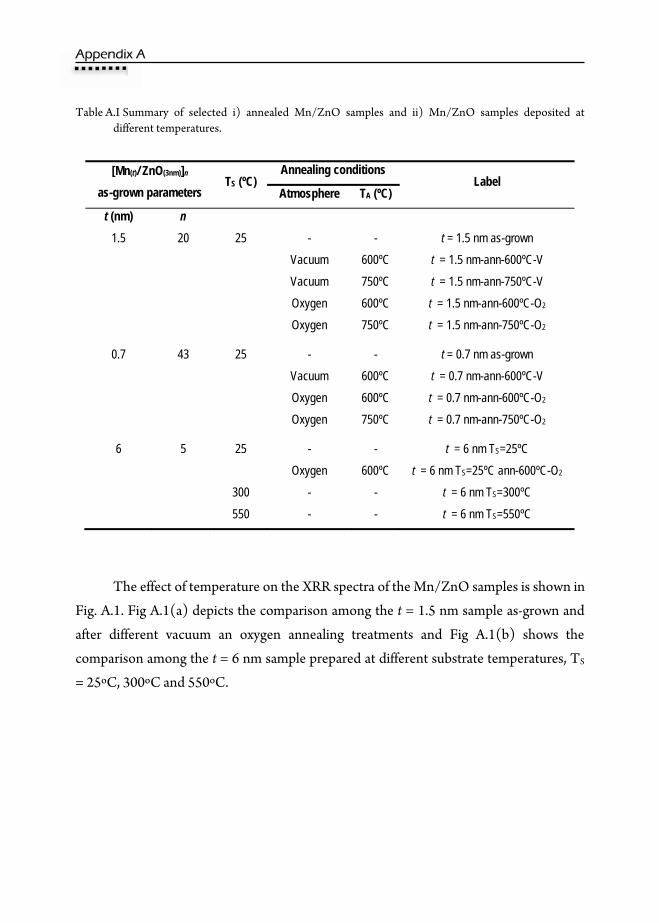
AAppppeennddiixx AA
Table A.I Summary of selected i) annealed Mn/ZnO samples and ii) Mn/ZnO samples deposited at different temperatures.
[Mn(t)/ ZnO(3nm)]n as-grown parameters
TS (ºC) Annealing conditions
Label Atmosphere TA (ºC)
t (nm) n 1.5 20 25 - - t = 1.5 nm as-grown
Vacuum 600ºC t = 1.5 nm-ann-600ºC-V Vacuum 750ºC t = 1.5 nm-ann-750ºC-V Oxygen 600ºC t = 1.5 nm-ann-600ºC-O2 Oxygen 750ºC t = 1.5 nm-ann-750ºC-O2 0.7 43 25 - - t = 0.7 nm as-grown Vacuum 600ºC t = 0.7 nm-ann-600ºC-V Oxygen 600ºC t = 0.7 nm-ann-600ºC-O2 Oxygen 750ºC t = 0.7 nm-ann-750ºC-O2 6 5 25 - - t = 6 nm TS=25ºC Oxygen 600ºC t = 6 nm TS=25ºC ann-600ºC-O2 300 - - t = 6 nm TS=300ºC 550 - - t = 6 nm TS=550ºC
The effect of temperature on the XRR spectra of the Mn/ZnO samples is shown in
Fig. A.1. Fig A.1(a) depicts the comparison among the t = 1.5 nm sample as-grown and
after different vacuum an oxygen annealing treatments and Fig A.1(b) shows the
comparison among the t = 6 nm sample prepared at different substrate temperatures, TS
= 25ºC, 300ºC and 550ºC.

Effect of Thermal Treatments and Substrate Temperature on Mn/ZnO Multilayers
125
Fig. A.1 (a) XRR spectra of sample t = 1.5 nm under different thermal treatments in comparison with as-
grown sample. (b) XRR spectra of sample t = 6 nm prepared at different substrate temperatures, TS = 25ºC, 300ºC and 550ºC.
As it can be inferred from the graphs, multilayer features, which are clearly
observed for the as-grown samples (TS = 25ºC), disappear when increasing
temperature. The loss of heterostructure periodicity is observed for i) annealing at a
temperature of 600ºC and higher (either in oxygen or vacuum) and also ii) when
growing at a substrate temperature of 300ºC or higher.
The fact that heterostructure features vanish at significant low temperature (TS =
300ºC) evidences high interdiffusion and strong interaction between the different layers.
These results suggest that, interface interaction, which becomes greatly favoured by
increasing temperature, also occurs in the as-grown samples. Therefore, moderate
diffusion in the Mn/ZnO samples series deposited at 25ºC could be then related to the
obtained coexistence of Zn-Mn-O wurtzite and rocksalt mixed phases in Mn/ZnO
multilayers with thicker Mn-rich layer thickness, supporting the obtained results in
Chapter 3.

AAppppeennddiixx AA
Two additional facts from the XRR graphs should be mentioned.
i) On one hand, the total thickness of t = 1.5 nm sample does not appreciably
change after annealing treatments. This has also been checked for t = 0.7 nm
sample annealed at 600ºC in oxygen flux, supporting the idea that thermal
treatments do no noticeably modify sample composition.
ii) On the other hand, sample thickness is significantly dependent of the substrate
temperature during growth. The deposition rate remarkably diminishes when
growing at TS higher than 25ºC, fact that we have also observed in the case of
Zn0.95Mn0.05O films grown at TS = 600ºC (section 5.6). The thickness of these
samples prepared with identical growth parameters except TS, has the following
behaviour: thickness of the t = 6 nm sample prepared at TS = 25ºC is 68 nm, it
becomes nearly one half (36.7 nm) for TS = 300ºC and it is finally reduced to 15.5
nm for TS = 550ºC.
For the sake of clarity, it should be noted that this sample series has been named as
“t = 6 nm” which corresponds to the nominal Mn layer thickness at 25ºC (tsput(Mn)
= 107 s, see Table A.I). For TS = 300ºC and 550ºC, although samples are named
in the same manner (t = 6 nm) in fact, expected Mn layer thickness are smaller for
these larger TS values. Moreover, it should be kept in mind that, for the two sample
series, i) and ii), no heterostructure arrangement was observed.
The Mn electronic states of several samples have been investigated by means of X-
ray absorption spectroscopy at the Mn K-edge and also at the Mn L3,2-edge.
The Mn K-edge XANES spectra of t = 1.5 nm as-grown as well as after annealing
treatments samples are shown in Fig A.2(a), in comparison with Mn0, Mn2+, Mn3+ and
Mn4+ spectra, from references.10
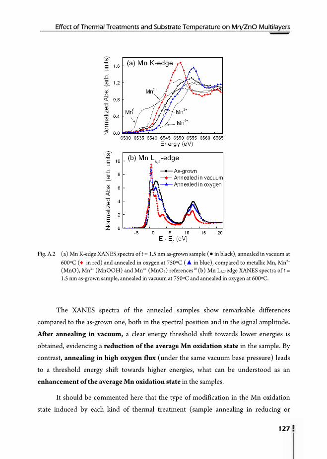
Effect of Thermal Treatments and Substrate Temperature on Mn/ZnO Multilayers
127
Fig. A.2 (a) Mn K-edge XANES spectra of t = 1.5 nm as-grown sample (● in black), annealed in vacuum at
600ºC (♦ in red) and annealed in oxygen at 750ºC (▲ in blue), compared to metallic Mn, Mn2+ (MnO), Mn3+ (MnOOH) and Mn4+ (MnO2) references10 (b) Mn L3,2-edge XANES spectra of t = 1.5 nm as-grown sample, annealed in vacuum at 750ºC and annealed in oxygen at 600ºC.
The XANES spectra of the annealed samples show remarkable differences
compared to the as-grown one, both in the spectral position and in the signal amplitude.
After annealing in vacuum, a clear energy threshold shift towards lower energies is
obtained, evidencing a reduction of the average Mn oxidation state in the sample. By
contrast, annealing in high oxygen flux (under the same vacuum base pressure) leads
to a threshold energy shift towards higher energies, what can be understood as an
enhancement of the average Mn oxidation state in the samples.
It should be commented here that the type of modification in the Mn oxidation
state induced by each kind of thermal treatment (sample annealing in reducing or

AAppppeennddiixx AA
oxidazing atmosphere) depends on the particular sample type, not pointing always
towards the same direction. For instance, the former observation can be compared to the
case of MnOx/ZnO samples (section 4.8), where annealing with oxygen flux under
identical conditions, implies a reduction of the Mn valence of the initially highly oxidized
Mn (instead of further oxidation).
The average Mn oxidation states in these samples have been calculated
considering the linear dependence between threshold energy and oxidation state for the
reference compounds, performed in the same way as it was done in section 3.8.1. The
estimated values are given in Table A.II. A total variation from +2.2 to +3.3 is found in
the Mn oxidation state, from the vacuum-annealed sample to the oxygen-annealed one.
Furthermore, the noticeable enhance of the white line observed for the annealed
samples might be assigned to an increase of the film crystal quality after thermal
treatment, what leads to a narrower distribution of Mn crystal environments.
Additional soft X-ray absorption experiments have been done at the Mn L3,2-edge
in order to obtain more information about the Mn electronic states in the samples. Fig.
A.2(b) shows the normalized XAS spectra measured at RT corresponding to t = 1.5 nm
as-grown sample and after annealing in vacuum at 750ºC and in oxygen at 600ºC.
It should be remarked that an experimental energy shift during data acquisition
made unattainable to know the precise energy threshold for each spectrum. For that
reason, E0 has been set as the maximum of the first derivate in Fig. A.2(b). Although the
actual energy shift among the different spectra cannot be inferred, a significant difference
in the Mn L3,2-edge spectral shape is clearly evidenced for the three samples. Hence, we
can still obtain important electronic information by analyzing the Mn L3,2-edge spectral
shapes, albeit being a bit more complicated.
By considering the Mn L3,2 XAS theoretical calculations for Mn2+ (d5), Mn3+ (d4)
and Mn4+ (d3) electronic configurations, which are described in section 2.6.2, we have
reasonably simulate the experimental spectra, simply by a linear combination of the
calculated ones in Td geometry under different crystal fields. It should be noted that the

Effect of Thermal Treatments and Substrate Temperature on Mn/ZnO Multilayers
129
assessment of the quality of the calculations is based on the correct reproduction of the
energy position of the different spectral features, relative energy separation and intensity
ratio. The linear combinations of the three Mn electronic states considered as well as the
obtained Mn oxidation state values are summarized in Table A.II, in comparison with the
above-estimated values from the Mn K-edge. Results are in rather good agreement. It can
also be noticed that the crystal field interaction magnitude included in the simulations
becomes smaller for the annealed samples, what might be associated with strain relaxation during the annealing process.
640 645 650 655 660 665
Inte
nsity
Energy (eV)
t = 1.5 nm
as-grown
vacuum-annealed
oxygen-annealed
0.35d5 + 0.65d4; 10Dq = 1 eV
d5; 10Dq = 0.5 eV
0.1d3 + 0.9d4; 10Dq = 0.5 eV
Fig. A.3 Mn L3,2 XAS spectra measured at RT of t = 1.5 nm sample, as grown, annealed in vacuum at
750ºC and annealed in oxygen at 600ºC. Spectra have been normalized and the L3 and L2 step edges have been subtracted by two arctan functions after background removal. Simulations (grey solid-lines) obtained by linear combinations of the calculations for Mn2+ (d5), Mn3+ (d4) and Mn4+
(d3) in Td crystal symmetry under different crystal field11 (10Dq = 0.5-1 eV) are included for comparison. More details of the calculation are given in section 2.6.2.

AAppppeennddiixx AA
Table A.II. Comparison between the Mn average oxidation state values estimated through the Mn K- and L3,2- edges.
[Mn (t)/ZnO(3nm)]n t = 1.5 nm; n = 20
Mn oxidation state (K-edge)
Mn oxidation state (L3,2-edge)
as-grown +2.6 ± 0.2 +2.65 (0.35Mn_d5+0.65Mn_d4; 10Dq=1)
ann-600ºC-V +2.2± 0.2 -
ann-750ºC-V - +2.0 (Mn_d5; 10Dq=0.5)
ann-600ºC-O2 - +3.1 (0.1Mn_d3+0.9Mn_d4; 10Dq=0.5)
ann-750ºC-O2 +3.3± 0.2 -
In addition, EXAFS experiments at the Mn- and Zn K-edges were performed for
several samples. The EXAFS Fourier Transforms (FT) at the Mn K-edge for
representative t = 1.5 nm as-grown and after different thermal treatments samples can be
seen in Fig. A.4. EXAFS analysis provides the pairs and distances summarized in Table
A.III, corresponding to the first and second coordination spheres. For the analysed k-
range interval, no significant differences were obtained when considering Mn or Zn as
backscatterer atoms. For that reason, only RMn-M distance contributions, where M stands
for both, Mn or Zn, are reported.
0 2 4 6 8
FT [k
2 χ(k
)]
Distance (Å)
as-grown
t = 1.5 nm
Mn K-edge
ann-750-O2
ann-600-V
Fig. A.4 EXAFS Fourier Transforms (FT) of for t = 1.5 nm as-grown, vacuum-annealed at 600ºC and
oxygen-annealed at 750ºC samples.

Effect of Thermal Treatments and Substrate Temperature on Mn/ZnO Multilayers
131
In Table A.III, results for the t = 1.5 nm as-grown sample, annealed in vacuum at
600ºC and in oxygen flux at 750ºC, as well as the t = 0.7 nm as-grown sample and
annealed in oxygen at 750ºC, are compared with references of manganese oxides and
zinc oxide.
From the obtained results and in agreement with the above XANES data, shorter
Mn-O distances are achieved for oxygen annealing while larger Mn-O distances are
found for vacuum annealing. Comparing with the manganese oxides references, Mn-O
and Mn-M distances in the vacuum-annealed t = 1.5 nm sample (Mn-O = 2.21 Å and
Mn-M = 3.13 Å) becomes very similar to those ones in MnO (Mn-O = 2.22 Å and
Mn-M = 3.14 Å).
The local environment around Mn for the oxygen-annealed t = 1.5 nm and t =
0.7 nm samples is very similar. For these samples, distances from the fits are Mn-O =
1.91 Å and Mn-M = 2.94 Å, being compatible, for instance, with MnO2 presence.
In comparison with t = 1.5 nm as-grown sample, Zn-O distances do not
appreciably change after vacuum annealing (2.04 Å), while they are reduced for oxygen
annealing (1.95 Å), becoming closer to those ones obtained in ZnO thin film (1.97 Å).
In general, it is found that coordination number increases after annealing,
especially for the second shell, what seems to be related to the crystalline quality improve
due to thermal treatment. The increase of the film crystal quality after thermal treatment
was also pointed above by the XANES spectra at the Mn K-edge.

AAppppeennddiixx AA
Table A.III. Summary of XAS results at the Mn and Zn K-edges corresponding to references and samples: XANES-obtained Mn oxidation values and R, N and σ2 EXAFS parameters (distance (R), number of neighbours (N) and Debye-Waller factor, respectively).
Mn
oxid.state Pair
R (Å)
N σ2 (10-3Å2)
References MnO +2 Mn-O 2.22 6 Mn-Mn 3.14 12 Mn3O4 +2 Mn-O 2.04 4 +3 Mn-O 1.93 4 2.28 2 Mn2O3 +3 Mn-O 1.89-2.25 6
β-MnO2 +4 Mn-O 1.89 6 Mn-Mn 2.89 2 Mn-Mn 3.40 8 ZnO Zn-O 1.99 4 Zn-Zn 3.23 12 Samples sputtered ZnO film Zn-O 1.97±0.02 4 0.4±0.5 Zn-Zn 3.18±0.02 12 12±1 t = 1.5 nm as-grown +2.6 Mn-O 1.94±0.02 3.6 2.5±0.5 Mn-M 2.86±0.02 1.6 20±1 Zn-O 2.05±0.02 2.9 1.4±0.5 Zn-Zn 3.14±0.02 5.0 4.5±1 t = 1.5 nm-ann-600-V +2.2 Mn-O 2.21±0.02 4.0 16.0±0.5 Mn-M 3.13±0.02 7.9 12±1 Zn-O 2.04±0.02 2.4 1.0±0.5 Zn-Zn 3.22±0.02 12.0 13±1 t = 1.5 nm-ann-750-O2 +3.3 Mn-O 1.91±0.02 3.2 1.0±0.5 Mn-M 2.93±0.02 9.2 23±1 Zn-O 1.95±0.02 4.0 9.6±0.5 Zn-Zn 3.30±0.02 10.0 8.5±1 t = 0.7 nm as-grown +2.9 Mn-O 1.92±0.02 2.9 3.0±0.5 Mn-M 2.91±0.02 1.9 30±1 t = 0.7 nm-ann-750-O2 +3.3 Mn-O 1.91±0.02 3.1 1.0±0.5 Mn-M 2.95±0.02 10.2 30±1

Effect of Thermal Treatments and Substrate Temperature on Mn/ZnO Multilayers
133
In order to obtain more structural information, XRD experiments were carried out
using synchrotron radiation. Grazing incidence (ω = 0.75º) as well as θ-2θ x-ray
diffraction measurements (with λ = 0.8857 Å) were performed.
Fig. A.5 (a) Grazing incidence (ω = 0.75º) x-ray diffraction of t = 1.5 nm sample (as-grown and annealed
in vacuum at 750ºC), oxygen-annealed (600ºC-O2) t = 0.7 nm sample and a 70 nm sputtered ZnO film. (b) Zoom of the grazing incidence sample spectra in comparison with XRD patterns of W-ZnO, MnO, Mn2O3 and Mn3O4 references.
Fig. A.5(a) shows grazing incidence spectra of t = 1.5 nm as-grown and vacuum-
annealed (ann-750ºC-V) samples, oxygen-annealed (ann-600ºC-O2) t = 0.7 nm sample
and a ZnO sputtered film (70 nm thickness), included for comparison. A zoom of these

AAppppeennddiixx AA
spectra, where ZnO MnO, Mn2O3 and Mn3O4 references have been included for
comparison, is depicted in Fig. A.5(b).
As it can be observed from both the XRD spectra, there exist important differences
among these samples. The comparison of the grazing incidence sample spectra with
reference spectra, in Fig. A.5(b), leads to the following results:
For the as-grown t = 1.5 nm sample, besides the major ZnO nanocrystals presence,
there are vestiges of Mn3O4 nanocrystalline grains. Since Mn2+ and Mn3+ cations coexist
in the Mn3O4, this result is in accordance with the average Mn oxidation state estimated
for this sample (+2.6 ± 0.2) and with the obtained EXAFS distances.
Vacuum-annealing of t = 1.5 nm sample at 750ºC greatly favours the
formation of MnO rocksalt nanocrystals, resulting in the principal crystalline phase
within the film, as it was found from EXAFS simulations. Apart from MnO,
nanocrystalline grains of ZnO, Mn2O3 and Mn3O4 are detected by XRD measurements.
The MnO crystal majority is consistent with the average Mn oxidation state calculated
for this sample (+2.2 ± 0.2).
From the spectrum of the oxygen-annealed sample (t = 0.7 nm-ann-600ºC-O2),
although a direct comparison with t = 1.5 nm sample cannot be made, it is possible to
deduce structural information. Thermal treatment in oxygen atmosphere leads to an
increase of the ZnO grain size, especially noticeable for the (101)-ZnO grains.
Although the major crystalline contribution comes from ZnO, there are also hints of
Mn3O4 in this sample. On the other hand, similarly to the case of Mn/ZnO as-grown
samples (Chapter 3), no traces of MnO2 grains have been found here, maybe due to their
amorphous character or the small crystalline grain size. Nevertheless, the obtained results
are compatible with the average Mn valence afore-estimated for this sample (+3.3 ± 0.2)
and with the EXAFS results.
In addition, the following results can be obtained from the θ-2θ sample scan,
shown in Fig. A.6.
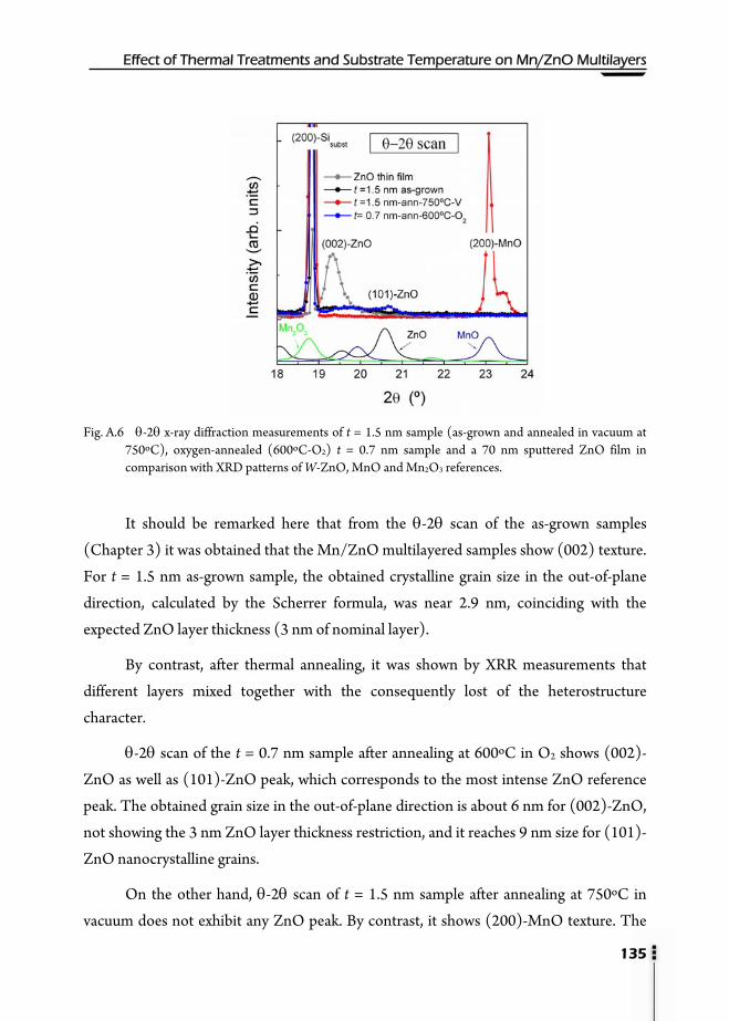
Effect of Thermal Treatments and Substrate Temperature on Mn/ZnO Multilayers
135
Fig. A.6 θ-2θ x-ray diffraction measurements of t = 1.5 nm sample (as-grown and annealed in vacuum at
750ºC), oxygen-annealed (600ºC-O2) t = 0.7 nm sample and a 70 nm sputtered ZnO film in comparison with XRD patterns of W-ZnO, MnO and Mn2O3 references.
It should be remarked here that from the θ-2θ scan of the as-grown samples
(Chapter 3) it was obtained that the Mn/ZnO multilayered samples show (002) texture.
For t = 1.5 nm as-grown sample, the obtained crystalline grain size in the out-of-plane
direction, calculated by the Scherrer formula, was near 2.9 nm, coinciding with the
expected ZnO layer thickness (3 nm of nominal layer).
By contrast, after thermal annealing, it was shown by XRR measurements that
different layers mixed together with the consequently lost of the heterostructure
character.
θ-2θ scan of the t = 0.7 nm sample after annealing at 600ºC in O2 shows (002)-
ZnO as well as (101)-ZnO peak, which corresponds to the most intense ZnO reference
peak. The obtained grain size in the out-of-plane direction is about 6 nm for (002)-ZnO,
not showing the 3 nm ZnO layer thickness restriction, and it reaches 9 nm size for (101)-
ZnO nanocrystalline grains.
On the other hand, θ-2θ scan of t = 1.5 nm sample after annealing at 750ºC in
vacuum does not exhibit any ZnO peak. By contrast, it shows (200)-MnO texture. The

AAppppeennddiixx AA
calculated MnO grain size in the out-of-plane direction is 42.5 nm, which is considerably
larger than, for instance, the 10.4 nm ZnO grain size.
No signs of metallic Mn or other Mn-Zn-O phases in these samples are evidenced
from XRD measurements. The main XRD results are summarized in Table A.IV.
Table A.IV Crystalline phases detected by grazing incidence XRD measurements for t = 1.5 nm sample (as-grown) and vacuum-annealed (750ºC-V), oxygen-annealed (600ºC-O2) t = 0.7 nm sample and a ZnO sputtered film. Crystalline grain sizes in the out-of-plane direction, calculated from θ-2θ diffraction peaks by means of the Scherrer equation, are also included.
[Mn(t)/ZnO(3nm)]n XRD-detected phases Out-of-plane grain size
t = 1.5 nm (as-grown) ZnO, Mn3O4 (002)-ZnO: 2.9 nm
t = 1.5 nm ann-750ºC-V MnO, ZnO, Mn2O3, Mn3O4 (200)-MnO: 42.5 nm
t = 0.7 nm ann-600ºC-O2 ZnO, Mn3O4 (101)-ZnO:9 nm; (002)-ZnO:6 nm
ZnO film (70nm) ZnO (002)-ZnO: 10.4 nm
Regarding the magnetic properties of these thermally treated samples, it can be
observed that, sample annealing, either in oxygen atmosphere or vacuum, leads to a
clear weakening of the ferromagnetic response. Magnetization versus temperature
dependence of t = 1.5 nm sample, as grown and after annealing, is shown in Fig. A.7.
The M(T) curve of the vacuum-annealed t = 1.5 sample reveals a magnetic
transition around 50 K, which can be related to the presence of Mn3O4 (TC = 43 K).
Furthermore, the existence of Mn3O4 grains has been verified in this sample by the above
XRD results.
Another fact to remark from the obtained M-T curves (Fig. A.7) is that the
ferromagnetic signal diminution is stronger when annealing in oxygen atmosphere
than in vacuum. It should be underlined that the significant reduction of the
ferromagnetic response by the oxygen effect has been commonly found in the Mn-Zn-O
system. For instance, we have also observed this effect for Zn0.95Mn0.05O films prepared in

Effect of Thermal Treatments and Substrate Temperature on Mn/ZnO Multilayers
137
oxygen atmosphere, as well as after annealing treatments in oxygen flow (section 5.6),
what evidences a generally unfavourable oxygen effect on the ferromagnetism of this
system.
50 100 150 200 250 300 350 4001
2
3
4
5
6
7
8
9M
agne
tizat
ion
(em
u/cm
3 )
Temperature (K)
as-grown
ann-750ºC-V
ann-750ºC-O2
t = 1.5 nm
Fig. .A.7 (a) M-T curves for the t = 1.5 nm sample as-grown and after different annealing treatments.
We can relate these results to the origin of the ferromagnetic response found in
Chapter 3 for Mn/ZnO multilayers. For the as-grown samples which exhibit
ferromagnetic order, Mn oxidation states close to +2 as well as coexistence of wurtzite
(W) and rocksalt (RS) phases were obtained. Nonetheless, the origin of the RTFM was
only ascribed to the presence of Zn-O-Mn wurtzite phase. For the case of smaller t values, high Mn oxidation states were obtained, resulting in the formation of MnO2
nano-sized grains and no appreciable FM. Keeping that in mind, the diminution of the
ferromagnetic signal after annealing could be understand in the following way:
Vacuum annealing at temperatures between 600-750ºC leads to a clear decrease of
the Mn oxidation state, which becomes near to +2. Mn oxidation states closer to +2 were
found to favour FM in Mn/ZnO multilayers. However, coexistence of Mn-Zn-O in W
and RS phases was obtained in samples with mostly Mn2+, being just Zn-O-Mn wurtzite
phase the responsible of the observed FM. Here, XRD has shown that MnO crystals (RS-
phase) are greatly favoured by vacuum annealing at these temperatures, as well as
crystallization of minority Mn2O3 or Mn3O4 phases. Both promoting RS phase over W

AAppppeennddiixx AA
phase and the stabilization of additional crystalline phases can explain the detrimental
effect on FM by vacuum annealing.
Annealing in oxygen flux at these temperatures, by contrast, leads to a clear
increase of the Mn oxidation state, which becomes about +3.3. Comparing to as-grown
Mn/ZnO multilayers with similarly oxidized Mn, mostly MnO2 nanograins embedded in
the W-ZnO matrix and no appreciable FM was obtained for these samples. Therefore,
the obtained diminution of the FM response after oxygen annealing agrees with the
origin of FM proposed in Mn/ZnO multilayers. The reduction of the ferromagnetism by
the oxygen effect has been commonly observed in the Mn-Zn-O system. V. K. Sharma et
al.3 showed that annealing in oxygen atmosphere at 800ºC reduced the magnetization
and sample became completely paramagnetic and E. Chikoidze et al.5 did not observe
any ferromagnetism in oxygen-annealed Mn-Zn-O films, which became highly unstable
at temperatures as low as 300ºC. Along the presented work, we have also observed
deterioration of the ferromagnetic signal due to oxygen in Zn0.95Mn0.05O films prepared
in oxygen atmosphere, as well as after annealing treatments in oxygen flow (section 5.6).
It should be noticed that in both cases, vacuum and oxygen annealing, additional
factors related to the loss of the heterostructure periodicity or to the strong modifications
of the crystalline grains after annealing can complicate this simplified image.
On the other hand, Fig A.8 shows the M(T) curves obtained for t = 6 nm samples
prepared at different substrate temperatures (TS = 25ºC and 300ºC) as well as oxygen-
annealed at 600ºC (TS = 25ºC). As it was found above for the t = 1.5 nm sample, oxygen
annealing of the t = 6 nm sample involves a significant reduction of the magnetization.
Furthermore, sample growth under similar experimental conditions but at moderate
substrate temperatures does not favour FM ordering in these samples. The obtained
results are compatible with the investigations performed by Pradhan et al.9, where it was
found that for substrate temperatures over 500ºC, the crystalline quality of the Zn1-
xMnxO films increased at the expense of a decrease in the RTFM due to the formation of
Mn related clusters. The declination of the FM occurs here even at lower substrate
temperatures.
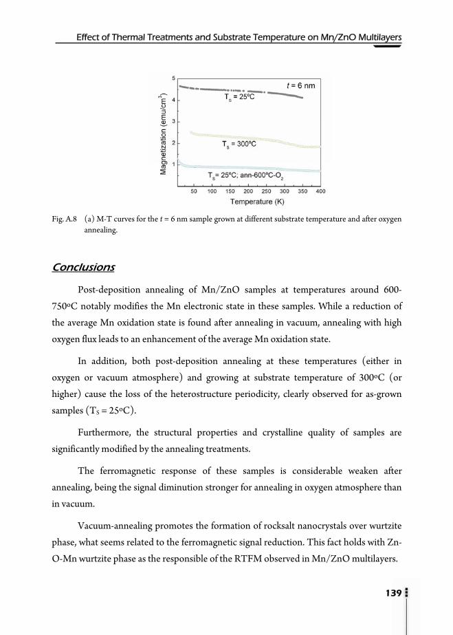
Effect of Thermal Treatments and Substrate Temperature on Mn/ZnO Multilayers
139
Fig. A.8 (a) M-T curves for the t = 6 nm sample grown at different substrate temperature and after oxygen
annealing.
Conclusions
Post-deposition annealing of Mn/ZnO samples at temperatures around 600-
750ºC notably modifies the Mn electronic state in these samples. While a reduction of
the average Mn oxidation state is found after annealing in vacuum, annealing with high
oxygen flux leads to an enhancement of the average Mn oxidation state.
In addition, both post-deposition annealing at these temperatures (either in
oxygen or vacuum atmosphere) and growing at substrate temperature of 300ºC (or
higher) cause the loss of the heterostructure periodicity, clearly observed for as-grown
samples (TS = 25ºC).
Furthermore, the structural properties and crystalline quality of samples are
significantly modified by the annealing treatments.
The ferromagnetic response of these samples is considerable weaken after
annealing, being the signal diminution stronger for annealing in oxygen atmosphere than
in vacuum.
Vacuum-annealing promotes the formation of rocksalt nanocrystals over wurtzite
phase, what seems related to the ferromagnetic signal reduction. This fact holds with Zn-
O-Mn wurtzite phase as the responsible of the RTFM observed in Mn/ZnO multilayers.
AAppppeennddiixx AA
Oxygen-annealing favours the formation of highly oxidized manganese phases
coexisting with W-ZnO, what leads to a decrease of FM, in accordance to the case of
Mn/ZnO multilayer with very thin Mn layers. The reduction of the ferromagnetic
response by the oxygen effect has been commonly observed in the Mn-Zn-O system.
Moreover, annealing favours the crystallization of additional phases, as Mn2O3 or
Mn3O4.
In addition to the Zn-O-Mn wurtzite phase declination, different facts as, loss of
the heterostructure periodicity, improvement of the crystal quality and formation of
additional crystal phases as Mn2O3 or Mn3O4 worsen the ferromagnetic order in the Mn-
Zn-O system.
References 1 H. K. Yadav, K. Sreenivas and V. Gupta, J. Appl. Phys. 99, 083507 (2006).
2 F. Pan, C. Song, X. J. Liu, Y. C. Yang and F. Zeng, Materials Science and Engeneering R 62, 1-35 (2008).
3 V. K. Sharma and G. D. Varma, J. Alloy. Compd. 458, 523 (2008).
4 B. Babić-Stojić, D. Milivojević, J. Blanuša, V. Spasojević, N. Bibić, B. Simonović and D. Arandelović J. Phys.: Condens. Matter 20, 235217 (2008).
5 E. Chikoidze, Y. Dumont, H. J. von Bardeleben, J. Gleize, O. Gorochov, J. Magn. Magn. Mater. 316, e181 (2007).
6 S. Lee, Y. Shon, S-W Lee, S. J. Hwang, H. S. Lee, T. W. Kang and D. Y. Kim, Apl. Phys. Lett. 88, 212513 (2006).
7 Y. W. Heo, M. P. Ivill, K. Ip, D. P. Norton, Appl. Phys. Letter 84, 2292 (2004).
8 P. Sharma, A. Gupta, K. V. Rao, F. J. Owens, R. Sharma, R. Ahuja, J. M. Osorio, Gullen, B. Johansson, G. A. Gehring, Nat. Mater. 2, 673 (2003).
9 A. K. Pradhan, K. Zhang, S. Mohanty, J. B. Dadson, and D. Hunter, Appl. Phys. Lett 86, 152511 (2005).
10 D. A. McKeown and J.E. Post, Am. Mineral. 86, 701 (2001).
11 G. van der Laan and I. W. Kirkman, J. Phys.: Condens. Matter 4, 4189 (1992).
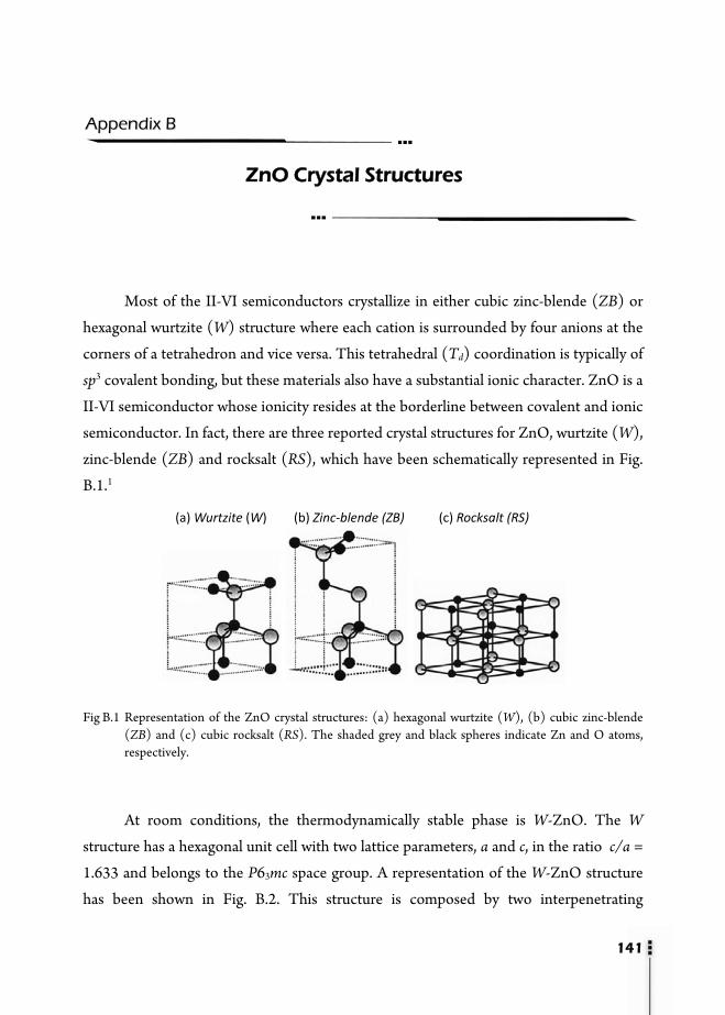
141
Most of the II-VI semiconductors crystallize in either cubic zinc-blende (ZB) or
hexagonal wurtzite (W) structure where each cation is surrounded by four anions at the
corners of a tetrahedron and vice versa. This tetrahedral (Td) coordination is typically of
sp3 covalent bonding, but these materials also have a substantial ionic character. ZnO is a
II-VI semiconductor whose ionicity resides at the borderline between covalent and ionic
semiconductor. In fact, there are three reported crystal structures for ZnO, wurtzite (W),
zinc-blende (ZB) and rocksalt (RS), which have been schematically represented in Fig.
B.1.1
Fig B.1 Representation of the ZnO crystal structures: (a) hexagonal wurtzite (W), (b) cubic zinc-blende (ZB) and (c) cubic rocksalt (RS). The shaded grey and black spheres indicate Zn and O atoms, respectively.
At room conditions, the thermodynamically stable phase is W-ZnO. The W
structure has a hexagonal unit cell with two lattice parameters, a and c, in the ratio c/a =
1.633 and belongs to the P63mc space group. A representation of the W-ZnO structure
has been shown in Fig. B.2. This structure is composed by two interpenetrating
(c) Rocksalt (RS)(b) Zinc‐blende (ZB)(a) Wurtzite (W)
AAppppeennddiixx BB
ZnO Crystal Structures

AAppppeennddiixx BB
hexagonal-close-packed (hcp) sublattices, each of which consists of one atom displaced
with respect to each other along the threefold c-axis by the amount of u = 3/8 = 0.375, in
an ideal W structure. Each atom type (group II or VI) is surrounded by 4 atoms of the
other kind, which are coordinated at the edges of a tetrahedron. In a real ZnO crystal, the
W structure deviates from the ideal arrangement by changing the c/a ratio or the u value.
There is a strong correlation between the c/a ratio and the u parameter. When the c/a ratio decreases, the u parameter increases in such a way that those four Td distances
remain nearly constant through a distortion of tetrahedral angles due to long-range polar
interactions.1,2
Fig B.2 Schematic representation of a ZnO wurtzite structure with lattice constants a in the basal plane and c in the basal direction; u parameter is expressed as the bond length or the nearest-neighbour distance b divided by c (0.375 in an ideal crystal) and α and β (109.47º in an ideal crystal) are the bond angles.
The ZB-ZnO structure is metastable and can be stabilized only by heteroepitaxial
growth on cubic substrates, such as ZnS.3 The symmetry of the ZB structure is given by
space group F43m and consists of two interpenetrating face-centered-cubic (fcc)
sublattices shifted along the body diagonal by one-quarter of a body diagonal. There are
four atoms per unit cell and every atom (group II) has Td coordination of atoms of the
other type (group VI), and vice versa. Because of the Td coordination of W and ZB
ZnO Crystal Structures
143
structures, the 4 nearest neighbours and 12 next-nearest neighbours have the same bond
distance in both structures. The main difference between them lies in the stacking
sequence of the closed-packed biatomic planes. While W-ZnO exhibits triangularly
arranged alternating biatomic closed-packed (0001) planes (AaBbAaBb…) in the
<0001> direction, ZB-ZnO consists of triangularly arranged atoms in the closed-packed
(111) planes along the <111> direction with a stacking order of AaBbCcAaBbCc… ,
referring small and large letters to the two different constituents.1
Additionally, as it happens in other II-VI semiconductors, W-ZnO can be
transformed to the RS-ZnO structure (NaCl) at relatively modest external pressures. The
reason for this is that the reduction of the lattice dimensions causes the interatomic
Coulomb interaction to favour the ionicity more over the covalent nature. The space-
group symmetry of the RS phase is Fm3m, and the structure is sixfold coordinated,
having octahedral (Oh) symmetry.1 However, the RS-ZnO structure cannot be stabilized
by epitaxial growth. Usually, the pressure induced phase transition occurs at
approximately 10 GPa, with a volume decrease of about 17%.4 Authors have reported
metastability of this phase for long periods of time even at room pressure and above
100ºC, and more recently, even when the pressure is released.1,5,6 By contrast, it has been
also reported that this transition is reversible at room temperature.1,7 Recently, ab initio calculations8 have been performed to study the mechanism responsible for the W-to-RS
structural phase transition in ZnO. It has been shown that the commonly observed
transition from the fourfold coordinated W to the sixfold coordinated RS phase occurs
through a quasitetragonal deformation which links, in a crystallographic simple way, the
two endpoint structures. The recently suggested hexagonal path does not seem favorable
for ZnO, although it seems possible in wurtzite semiconductors such as AlN or SiC). The
discussed paths for the phase transformation in the ab angle (γ) - u internal coordinate
plane is shown in Fig. B.3.
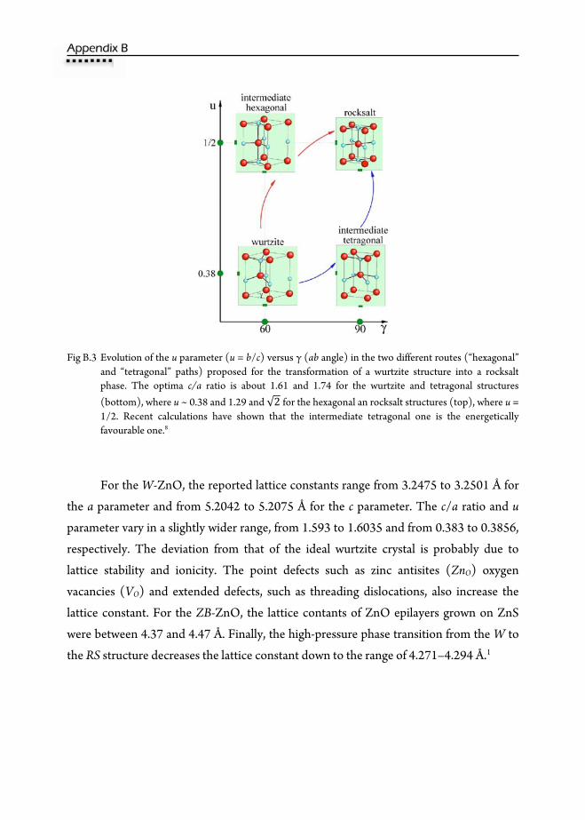
AAppppeennddiixx BB
Fig B.3 Evolution of the u parameter (u = b/c) versus γ (ab angle) in the two different routes (“hexagonal” and “tetragonal” paths) proposed for the transformation of a wurtzite structure into a rocksalt phase. The optima c/a ratio is about 1.61 and 1.74 for the wurtzite and tetragonal structures (bottom), where u ~ 0.38 and 1.29 and √2 for the hexagonal an rocksalt structures (top), where u = 1/2. Recent calculations have shown that the intermediate tetragonal one is the energetically favourable one.8
For the W-ZnO, the reported lattice constants range from 3.2475 to 3.2501 Å for
the a parameter and from 5.2042 to 5.2075 Å for the c parameter. The c/a ratio and u parameter vary in a slightly wider range, from 1.593 to 1.6035 and from 0.383 to 0.3856,
respectively. The deviation from that of the ideal wurtzite crystal is probably due to
lattice stability and ionicity. The point defects such as zinc antisites (ZnO) oxygen
vacancies (VO) and extended defects, such as threading dislocations, also increase the
lattice constant. For the ZB-ZnO, the lattice contants of ZnO epilayers grown on ZnS
were between 4.37 and 4.47 Å. Finally, the high-pressure phase transition from the W to
the RS structure decreases the lattice constant down to the range of 4.271–4.294 Å.1
ZnO Crystal Structures
145
References
1 Ü. Özgür, Ya. I. Alivov, C. Liu, A. Teke, M. A. Reshchikov, S. Dogan, V. Avrutin, S. J. Cho,
and Morkoς, Applied Physics Reviews, J. Appl. Phys. 98, 0141301 (2005).
2 E. Kisi and M. Elcombe, Acta Crystallogr., Sect. C: Cryst. Struct. Commun. C45, 1867 (1989).
3 T. Kogure and Y. Bando, Y. Electron Microsc. 47, 7903 (1993).
4 C. H. Bates, W. B. White, and R. Roy, Science 137, 993 (1962).
5 L. Gerward and J. S. Olsen, J. Synchrotron Radiat. 2, 233 (1995).
6 J. M. Recio, R. Pandey, and V. Luaña, R. Pandey, L. Gerward, and J. Staun Olsen, Phys. Rev. B 58, 8949 (1998).
7 J. C. Jamieson, Phys. Earth Planet. Inter. 3, 201 (1970).
8 A. M. Saitta and F. Decremps, Phys. Rev. B 70, 035214 (2004).


PART II
Mn-Si3N4 System


147
6.1. Motivation
Manganese nitrides have gained attention among the 3d transition metal nitrides
for their variety of electronic and magnetic properties which are suitable for potential
applications.1,2,3 Recently, these materials have also generated interest in the field of
diluted magnetic semiconductors (DMSs) with high Curie temperatures, as potentially
magnetic secondary phases forming within films of Mn-doped III-V semiconductors
such as Mn:GaAs, MnInN and especially Mn:GaN.4,5,6
The manganese nitrides form a variety of stoichiometric phases (ε, ζ, η, θ)
exhibiting different magnetic properties. The most N rich phase, mononitride θ-MnN,
has a tetragonally distorted rocksalt (NaCl) structure with an antiferromagnetic (AF)
ground state. It usually contains a considerable amount of N vacancies and is often
labeled as Mn6N5+x.7 The closely related η-Mn3N2 phase is also of the NaCl structure but
with an ordered array of N vacancies.7,8 The ζ-phases (Mn5N2 and Mn2N) have
hexagonal closed packed arranges and present ferromagnetic (FM) and AF order,
respectively9. Finally, the ε-Mn4N phase consists basically in a Mn face-centered cubic
structure with an interstitial N and exhibits ferrimagnetism with a curie temperature (TC)
as high as 745 K.10
These MnNx phases are currently related to inhomogeneities in ternary nitride-
based alloys as the possible origin of the observed ferromagnetism. Recent studies have
pointed towards Mn4N as a segregation phase showing the ferromagnetic behaviors in
Mn:GaN films.5 Special attention has been also directed to the θ-MnN phase, since
possible inclusions or MnN-rich regions in the matrix can have the same crystallographic
structure as the semiconductor host. Although MnN has an AF ground state, it has been
CChhaapptteerr 66
Mn/Si3N4 Multilayers
CChhaapptteerr 66
theoretically shown that FM order can be established depending on the polymorph of
MnN and lattice parameters.6 A number of band-structure calculations have been
performed considering MnN in the hypothetical zinc-blende (ZB) and wurtzite (W)
structures in order to get a better comprehension of these ternary nitride-based DMS
systems.6,11 Ferromagnetism with TC of 354 K due to Mn-rich precipitates in the zinc-
blende phase has been recently predicted in Mn:GaN by using the mean-field
approximation.4 More recently, simulations of GaN/MnN superlattices have been
developed as a new way to obtain the FM W-MnN on GaN as an alternative to the
(Ga,Mn)N DMS approach.12 These calculations based on spin-density-functional theory
have suggested that this system can be used for new spintronics devices as they can
provide spin-polarized carriers in the wide-gap nitride systems. A FM ground state has
been predicted in these GaN/MnN heterostructures, which comprise a thin layer of
biaxially strained W-MnN intercalated with layers of GaN, due to the structure relaxation
at the GaN-MnN interface.
Despite all these exciting properties, up to date there have not been reported
experimental efforts to obtained FM semiconductor/manganese nitride
heterostructures. Even the interesting magnetic properties of MnNx films have hardly
been experimentally studied, probably due to difficulties in sample preparation. Just a few
attempts of fabrication of MnN by reactive sputtering9 and ion-assisted deposition2,
Mn3N2 using reactive sputtering3 and molecular beam epitaxy1 and Mn4N, also by
reactive sputtering,3,13 have been reported.
Here, because of its similarities, instead of GaN, we use Si3N4, which also possesses
a wide-band-gap semiconducting behavior and can be an excellent host material due to
its possible high dopant concentration.14,15 Furthermore, Si3N4 has been extensively used
in materials science for its good performance in resistance to thermal shock and
oxidation, great chemical stability, low density, and high fracture toughness.16,17 Recently,
there have been reported successful researches on Si3N4 films, nanowires and nanobelts,
which are very promising for the synthesis of nanostructured Si3N4 on a large scale.18,19,20

Mn/Si3N4 Multilayers
149
Details of the Si3N4 crystal structure have been included as additional information
at the end of Chapter 6.
In the present chapter, the magnetic properties of several series of Mn/Si3N4
multilayered films have been explored and ferromagnetism above room temperature has
been found in this system for the first time. The structural and electronic properties of
the samples have been studied using a number of techniques as x-ray reflectivity, x-ray
absorption and x-ray photoemission spectroscopies and x-ray magnetic circular
dichroism to investigate the magnetic-structural relationship in the Mn/Si3N4 system.
Different sets of Mn/Si3N4 multilayers have been prepared by varying the
Mn:Si3N4 relative ratio. The evolution of the magnetic properties has been studied for
multilayers with nominal formula [Mn(tm)/Si3N4(3nm)]n, being “tm” the nominal Mn
layer thickness and “n” the number of bilayers, as well as for samples labeled as
[Mn(0.6nm)/Si3N4(tsn)]43, being “tsn” the nominal Si3N4 layer thickness, in order to find
the most suitable conditions to stabilize the ferromagnetic ordering in this system.
4.2. Preparation of multilayers
Mn/Si3N4 multilayers were prepared by sequential sputtering of Si3N4 and Mn on
Si(100) substrates at RT. The residual pressure in the vacuum system was in the 1 x 10⁻⁷
mbar range. The Si3N4 layers were deposited by reactive RF-sputtering from a pure Si
target (Goodfellow: 99.999 %) with N2 as reactive sputtering gas.21 The deposition rate
was 2 nm/min for a RF power of 100 W. Mn was grown by DC-sputtering from a Mn
target (Goodfellow: 99.95 %) with Ar as sputtering gas and a deposition rate of ~4
nm/min for a DC power of ~ 10 W.
Samples with nominal formula [Mn(tm)/Si3N4(3nm)]n as well as samples named
[Mn(0.6nm)/Si3N4(tsn)]43 were prepared. For the first set of samples, the Si3N4 layer
thickness was maintained constant while the Mn layer (tm) was modified between 6 and
0.1 nm of nominal thickness. In this case, the number of bilayers (n) was progressively
increased (from 5 to 75) as the Mn layer thickness was reduced in order to maintain the
total amount of Mn approximately constant. In the case of [Mn(0.6nm)/Si3N4(tsn)]43

CChhaapptteerr 66
samples, the Mn layer thickness was kept approximately constant while the Si3N4 layer
thickness (tsn) was modified from 6 nm to 0.7 nm. In the former case, the number of
bilayers was always the same (n = 43). For the two sets of multilayers the growth process
began with a Si3N4 layer and terminated by depositing an additional 3 nm Si3N4 layer on
top.
6.3. X-Ray Reflectivity (XRR)
X-ray reflectivity measurements were done in a standard X-ray diffractometer
(Bruker D8) working with the Cu Kα wavelength, at the ICMM facilities. XRR spectra of
the studied multilayers are shown in Fig. 6.1 for both samples series prepared with
different Mn-layer thickness (tm) (Fig. 6.1(a)) and with variable Si3N4 layer thickness
(tsn) (Fig 6.1 (b)).
Well-defined peaks of heterostructure periodicity in the out-of-plane direction
can be observed in the spectra from samples with larger tm and tsn thicknesses, while these
periodicity features become smoother as tm and tsn are reduced. In fact, non-continuous
Mn layers are expected for very small tm values, where Mn layer thickness and interface
roughness become comparable. It should be noted in Fig. 6.1(a) that samples with a large
bilayer number, as for instance 75 bilayers, have a total thickness too large to exhibit the
short oscillations corresponding to finite size film interferences.
Sample description and microstructural features such as average bilayer thickness
are summarized in Tables 6.I and 6.II for samples with variable tm and tsn, respectively.
Measured layer thickness is approximately 15 % higher than nominal.
For the sake of clarity, samples will be named from now on by their XRR
experimentally obtained thickness values.

Mn/Si3N4 Multilayers
151
1 2 3 4 5 6
Inte
nsity
(a. u
.)
tm=3.8 nm (x10)
tm=1.9 nm (x20)
tm=0.86 nm (x43)
tm=0.5 nm (x75)
tm=0.28 nm (x75)
tm=7.6 nm (x5)
tm=5.4 nm (x8)
[Mn(tm)/Si3N4(3.4nm)]n (a)
2θ (º)
tsn=1.6 nm
tsn=1.0 nm
tsn=6.7 nm
tsn=3.4 nm
[Mn(0.7nm)/Si3N4(tsn)]43 (b)
Fig. 6.1. (a) XRR spectra of some of the multilayer samples with different Mn-layer thickness (tm). Experimental tm values are shown in the figure. (b) XRR spectra of the prepared samples with different Si3N4-layer thickness (tsn). Experimental tm values are shown in the figure. All spectra have been vertically shifted for clearness.

CChhaapptteerr 66
Table 6.I. Description of selected [Mn(tm)/Si3N4(3nm)]n nominal samples: nominal Mn thickness (tm), number of bilayers (n), nominal bilayer thickness (Λ), XRR- obtained bilayer thickness (XRR-Λ), XRR- obtained Mn thickness (XRR-tm) and atomic composition, obtained from simulation of RBS and NRA.
Nominal
tm (nm)
n Nominal
Λ (nm)
XRR- Λ
(nm)
Mn-layer atomic density
(at./cm2)
XRR- tm
(nm)
Composition (% at)
[Mn] [ Si] [N]
6 5 9 11 4.6x10¹⁶ 7.6 0.42 0.14 0.44
6 5 9 10.7 - 7.3 - - -
4 8 7 8.8 - 5.4 - - -
3 10 6 6.9 2.2x10¹⁶ 3.8 0.31 0.16 0.53
3 10 6 6.6 - 3.5 - - -
1.5 20 4.5 5.3 1.1 x10¹⁵ 1.9 0.25 0.18 0.57
0.7 43 3.7 4.2 5.9 x10¹⁶ 0.86 0.17 0.25 0.58
0.4 75 3.4 3.6 4.1 x10¹⁵ 0.5 0.13 0.28 0.59
0.2 75 3.2 3.4 2.9 x10¹⁵ 0.28 0.10 0.30 0.60
0.1 75 3.1 3.1 1.9 x10¹⁵ 0.17 0.07 0.35 0.59
Table 6.II. Description of selected [Mn(0.6nm)/Si3N4(tsn)]43 nominal samples: nominal Si3N4 thickness (tsn), number of bilayers (n), nominal bilayer thickness (Λ), XRR- obtained bilayer thickness (XRR- Λ), XRR- obtained Si3N4 thickness (XRR- tsn) and atomic composition, obtained from simulation of RBS and NRA.
Nominal
tsn (nm)
n Nominal
Λ (nm)
XRR- Λ
(nm)
Mn-layer atomic density
(at./cm2)
XRR- tsn
(nm)
Composition (% at)
[Mn] [ Si] [N]
6 43 6.6 7.4 4.7x10¹⁵ 6.7 0.08 0.34 0.58
3 43 3.6 4.1 4.8x10¹⁵ 3.4 0.13 0.27 0.60
1.5 43 2.1 2.3 4.8x10¹⁵ 1.6 0.20 0.20 0.60
0.7 43 1.7 1.7 4.7x10¹⁵ 1.0 0.25 0.14 0.61

Mn/Si3N4 Multilayers
153
6.4. Transmission Electron Microscopy (TEM)
For several samples, the multilayer periodicity has been additionally confirmed
by transmission electron microscopy studies performed in collaboration with Dr.
Augusto Barrós and Dr. Mercedes Vila from the Department of Ceramics and Glass
Engineering, CICECO, at the University of Aveiro, in Portugal. The TEM cross-section
images corresponding to tm = 3.8 nm and 0.86 nm samples are depicted in Fig. 6.2(a) and
6.2(b) respectively. For the tm = 3.8 nm sample, the image shows continuous layers of
similar thickness corresponding to the Mn-rich and Si3N4 layers. An interface roughness
enhance as the number of layers increases is evidenced in Fig. 6.2(a). The total thickness
obtained by TEM is approximately 70 nm for this sample, which is slightly smaller but
quite in agreement with XRR measurements. Conversely, although z-axis periodicity is
still observed from TEM image of the tm = 0.86 nm sample, the image suggests non-
continuous growth in this former case. Non-continuous layers Mn-rich layers are hence
expected for samples with tm < 0.86 nm.
Fig. 6.2 (a) Cross-sectional TEM image of the sample labeled as [Mn(3.8nm)/Si3N4(3.4nm)]10 and (b) [Mn(0.86nm)/Si3N4(3.4nm)]43 sample, performed in a 300 kV Hitachi H9000-NA microscope.

CChhaapptteerr 66
6.5. Rutherford Backscattering Spectroscopy (RBS) and Nuclear Reaction Analysis (NRA)
Rutherford backscattering spectroscopy (RBS) and Nuclear Reaction Analysis
(NRA) experiments were carried out at the Centro Nacional de Aceleradores (Sevilla,
Spain) in collaboration with Dr. Javier García López to determine precisely the atomic
composition of the samples. For the RBS experiments, a 2 MeV H2+ beam was employed,
with beam diameter ∼ 1 mm and scattering angle of 165º. The NRA measurements were
done using the 14N(d,α1)12C nuclear reaction with a 1.4 MeV D+ beam and a detection
angle of 150º. A 13 μm thick mylar foil was placed in front of the detector in order to stop
the backscattered deuterons to avoid saturation of the electronic set-up. For absolute N
quantification of our samples, we have used as standard a 100 nm thick Si3N4 film grown
on Si substrate.
Fig. 6.3(a) and 6.3(b) show the obtained RBS spectra and their corresponding
simulations using the SIMNRA simulation software package. The calculated Mn atomic
density and film atomic composition obtained jointly by RBS and NRA for some
representative samples are summarized in Tables 6.I and 6.II.
A comparison between the experimental manganese layer thickness values
obtained from XRR spectra and the ones calculated from RBS data considering pure
metal manganese density is shown in Fig. 6.4. The obtained difference means that, even if
pure Mn was sputtered, layers do not consist of pure metallic Mn, since to obtain the
actual thickness (given by the XRR data) a smaller Mn density should be considered in
calculations from RBS. On the other hand, no appreciable oxygen amount was detected
by RBS and NRA experiments (less than 5 at. %). Both, the reduced Mn density
evidenced from RBS simulations and the small oxygen content indicate that manganese
nitridation occurs at the Mn-rich layers.
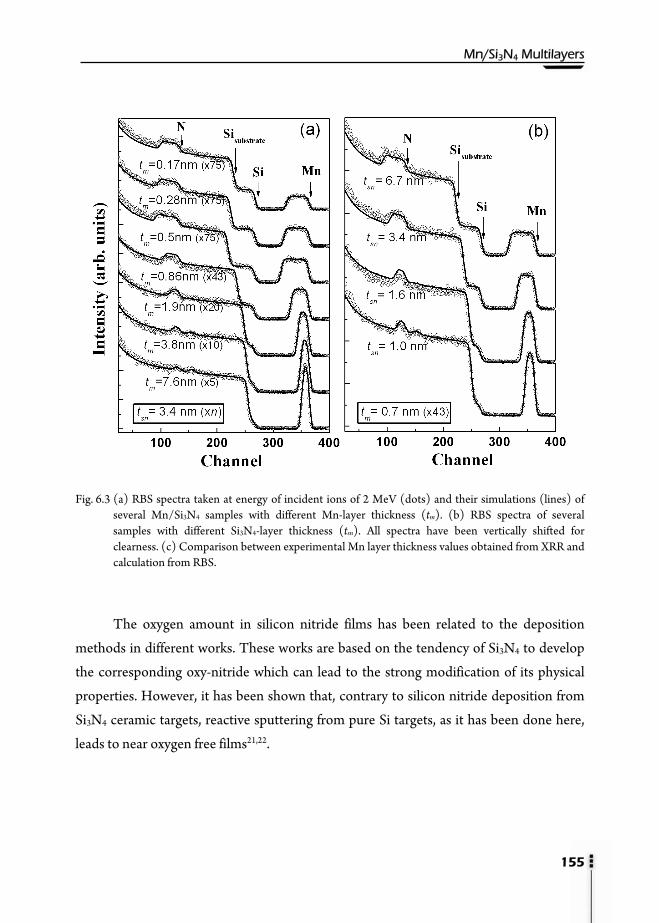
Mn/Si3N4 Multilayers
155
Fig. 6.3 (a) RBS spectra taken at energy of incident ions of 2 MeV (dots) and their simulations (lines) of
several Mn/Si3N4 samples with different Mn-layer thickness (tm). (b) RBS spectra of several samples with different Si3N4-layer thickness (tsn). All spectra have been vertically shifted for clearness. (c) Comparison between experimental Mn layer thickness values obtained from XRR and calculation from RBS.
The oxygen amount in silicon nitride films has been related to the deposition
methods in different works. These works are based on the tendency of Si3N4 to develop
the corresponding oxy-nitride which can lead to the strong modification of its physical
properties. However, it has been shown that, contrary to silicon nitride deposition from
Si3N4 ceramic targets, reactive sputtering from pure Si targets, as it has been done here,
leads to near oxygen free films21,22.

CChhaapptteerr 66
0 1 2 3 4 5 60
1
2
3
4
5
6
7
8
Expe
rimen
tal t
m (
nm)
Nominal Mn-layer thickness tm (nm)
RBSCalculated using metalMn density (7.45 g/cm3)
XRR
Fig. 6.4 Comparison between experimental Mn layer thickness values obtained from XRR and calculations
from RBS.
6.6. Magnetic properties
Magnetic characterization of samples was performed by means of a commercial
SQUID magnetometer (Quantum Design MPMS-5S) in the temperature range from 5
to 400 K at the ICMM facilities.
A ferromagnetic-like signal has been observed for most of the prepared
samples. The magnetic characterization results of the Mn/Si3N4 films are displayed in
Fig. 6.5. The magnetization per Mn atom has been calculated accounting for the precise
amount of Mn as obtained by RBS measurements. Fig. 6.5(a) shows the hysteresis loops
recorded at RT and 5 K for selected samples with tm ranging from 3.5 to 0.14 nm. In all
cases the diamagnetic contribution of the silicon substrate has been subtracted from the
recorded data. For the tm = 0.14 nm sample, a high paramagnetic-like component is
observed at first glance. While this sample exhibits a very weak ferromagnetic ordering,
the room temperature magnetization of the tm = 3.5 nm sample indicates the existence of
an average magnetic moment of ~ 0.4 μB per Mn atom.
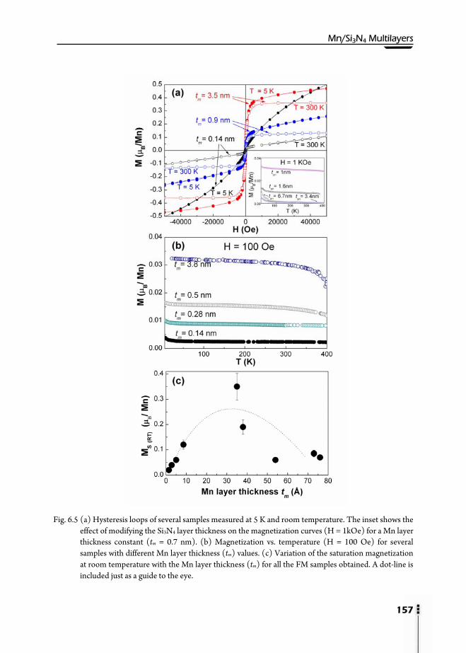
Mn/Si3N4 Multilayers
157
Fig. 6.5 (a) Hysteresis loops of several samples measured at 5 K and room temperature. The inset shows the
effect of modifying the Si3N4 layer thickness on the magnetization curves (H = 1kOe) for a Mn layer thickness constant (tm = 0.7 nm). (b) Magnetization vs. temperature (H = 100 Oe) for several samples with different Mn layer thickness (tm) values. (c) Variation of the saturation magnetization at room temperature with the Mn layer thickness (tm) for all the FM samples obtained. A dot-line is included just as a guide to the eye.

CChhaapptteerr 66
This value corresponds to about 110 emu/cm3 of film at RT, being this value the
highest saturation magnetization among the samples studied here. This sample shows a
coercive field (HC) ∼ 60 Oe at RT. Similar HC values at RT, between 50 and 80 Oe
approximately, are found for the whole set of samples, while they range between 80 and
130 Oe at 5 K.
The temperature dependence of magnetization, M(T), measured under an
applied magnetic field of 100 Oe, can be seen in Fig. 6.5(b). An ordering temperature
well above 400 K can be inferred for samples with tm ≥ 0.5 nm. For samples with smaller
tm, although an enhancement of TC could be evoked from the M-T curves, their smaller
ferromagnetic response together with the complexity of M versus T measurements over
400 K for thin film samples, make difficult to assert an increase of TC. The evolution of
the saturation magnetization (MS) at room temperature versus the measured Mn layer
thickness (tm) for all the obtained FM samples is represented in Fig. 6.5(c). For small
Mn layer thickness, MS increases with tm, exhibiting a maximum for a Mn layer
thickness of the order of the Si3N4 one (~3.5 nm) while MS decreases for further tm
increase.
The importance of the Si3N4 layer thickness into the magnetic properties is also
evidenced in the inset of Fig. 6.5(a), that shows the M(T) curves of several samples
prepared with constant Mn layer thickness (tm = 0.7 nm), same number of repetitions (n
= 43) and different Si3N4 layer thickness, tsn (ranging from 6.7 to about 1 nm). Although
it should be remarked that smaller magnetization values are found for this type of
samples, the highest FM signal within this series is obtained for the sample labeled as
[Mn(0.7nm)/Si3N4(1nm)]43. Considering that the sample having the highest MS value is
sample is [Mn(3.5nm)/Si3N4(3.4nm)]10, it seems that the ferromagnetic alignment is
favored when both, the manganese-rich and the silicon nitride layers have comparable
thicknesses.
It should be also underlined that, for extra samples series prepared under similar
experimental conditions, FM ordering and magnetization values of the same order were
always found in the case of samples prepared with silicon nitride layers of about 3 nm and

Mn/Si3N4 Multilayers
159
sufficiently thick Mn layers. However, magnetic properties were not always reproducible
when preparing additional similar samples with very thin layers, especially for Mn layers
(tm) thinner than 2 nm. None appreciable FM or mostly paramagnetic behaviour was
sometimes found in this case, suggesting either the metastability or the high sensitivity to
specific experimental conditions of the developed ferromagnetic phase, whose instability
appears to be enhanced in the non-continuous growth regime.
Additional characterizations, as XPS and XAS, have been focused in this work on
understanding the origin of the observed RTFM in this multilayer system.
6.7. X-Ray Photoemission Spectroscopy (XPS)
XPS measurements were carried out in collaboration with Dr. Elisa Román and
Dr. Yves Huttel at the ICMM. The measurements were performed in an ultra high-
vacuum (UHV) chamber with a base pressure of 1 x 10⁻¹⁰ mbar. The angle between the
hemispherical analyzer (Specs-PHOIBOS100) and the plane of the surface was kept at
60° and the x-ray radiation was the Mg Kα line (1253.6 eV). XPS spectra were recorded
at the core levels of the elements present in the samples (Mn, Si, N); in the case of Mn,
Mn 3p spectra were recorded with a photon energy step of 0.1 eV and pass energy of 15
eV in order to optimise the energy resolution for further fitting analysis and Mn species
identification. Prior to the data analysis, the contributions of the Mg Kα satellite lines
were subtracted and the spectra were subjected to a Shirley background subtraction
formalism. The binding energy (BE) scale was calibrated with respect to the Si peak at
101.6 eV. Fittings were carried out using Gaussian-Lorentzian doublets (GL). Within the
experimental conditions, the sensitivity to the surface is rather limited and it can be
assumed that the XPS spectra give information of the electronic structure that
corresponds to the bulk.
In order to study the electronic properties of Mn-rich layers, we have performed
an XPS study of two samples, the tm = 7.6 nm sample, representative of the thick Mn layer
samples, and the tm = 0.5 nm one, where non-continuous Mn is expected. Depth profiles
were performed by removing thin layers of material with a calibrated sputtering gun
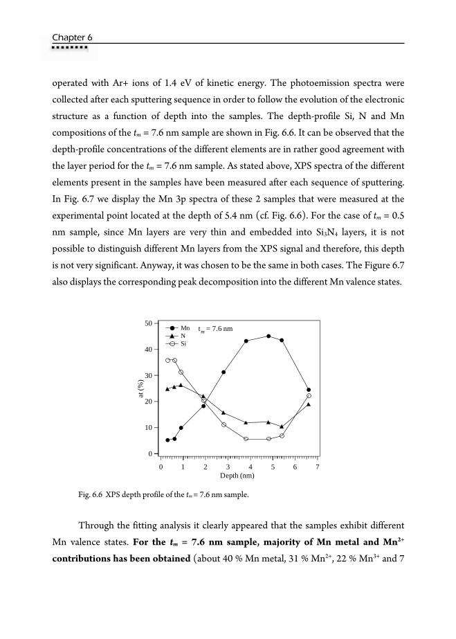
CChhaapptteerr 66
operated with Ar+ ions of 1.4 eV of kinetic energy. The photoemission spectra were
collected after each sputtering sequence in order to follow the evolution of the electronic
structure as a function of depth into the samples. The depth-profile Si, N and Mn
compositions of the tm = 7.6 nm sample are shown in Fig. 6.6. It can be observed that the
depth-profile concentrations of the different elements are in rather good agreement with
the layer period for the tm = 7.6 nm sample. As stated above, XPS spectra of the different
elements present in the samples have been measured after each sequence of sputtering.
In Fig. 6.7 we display the Mn 3p spectra of these 2 samples that were measured at the
experimental point located at the depth of 5.4 nm (cf. Fig. 6.6). For the case of tm = 0.5
nm sample, since Mn layers are very thin and embedded into Si3N4 layers, it is not
possible to distinguish different Mn layers from the XPS signal and therefore, this depth
is not very significant. Anyway, it was chosen to be the same in both cases. The Figure 6.7
also displays the corresponding peak decomposition into the different Mn valence states.
Fig. 6.6 XPS depth profile of the tm = 7.6 nm sample.
Through the fitting analysis it clearly appeared that the samples exhibit different
Mn valence states. For the tm = 7.6 nm sample, majority of Mn metal and Mn2+
contributions has been obtained (about 40 % Mn metal, 31 % Mn2+, 22 % Mn3+ and 7
50
40
30
20
10
0
at (%
)
76543210Depth (nm)
Mn N Si
tm = 7.6 nm

Mn/Si3N4 Multilayers
161
% Mn4+ are given from the fits, where an uncertainty between 5-10 % can be expected).
Despite the small additional contribution from higher oxidized species, if we consider the
majority species, the [Mn metal]/[Mn2+] ratio is about 4/3. For the tm = 0.5 nm
sample, mostly Mn2+ contribution was deduced from the XPS analysis (about 6 % Mn
metal, 65 % Mn2+, 20 % Mn3+ and 9 % Mn4+). The extra Mn3+ and Mn4+ high valence
contributions are approximately the same in both samples. However, the Mn metallic
phase is drastically reduced in this former sample, being the Mn2+ valence state the
dominant one. The obtained Mn average oxidation states are about +1.9 for the tm =
7.6 nm sample and +2.3 for the tm = 0.5 nm one.
Fig. 6.7 Mn 3p XPS spectra of the tm = 7.6 nm and tm = 0.5 nm samples with the corresponding
decomposition analysis into the different Mn valence states.

CChhaapptteerr 66
6.8. X-Ray Absorption Spectroscopy (XAS)
Aimed at determining the Mn electronic state, the local structure of the Mn sites and
the presence of Mn-N alloys, we have performed a combined XANES and EXAFS study of
the [Mn(tm)/Si3N4(3.4nm)]n and [Mn(0.7nm)/Si3N4(tsn)]43 samples.
6.8.1. X-Ray Absorption Near-Edge Structure (XANES)
XAS experiments at the Mn K-edge have been performed to study the Mn
electronic structure as well as the Mn atomic surrounding. The experiments were carried
out at the BM26 and BM8 beamlines of the European Synchrotron Radiation Facility
(ESRF) in Grenoble. Samples were measured in fluorescence and TEY modes,
respectively. No appreciable differences were found between the two detection modes
and spectra are included here without distinction. Further details of the experimental set-
up are given in section 2.6.1
The normalized Mn K-edge XANES spectra of representative samples are shown
in Fig. 6.8. The threshold energy position evidences an average Mn oxidation state
close to 2+, in agreement with XPS results. Details of the pre-peak region can be seen in
the inset, showing an evolution of the pre-peak intensity from the manganese foil
reference to the samples with thinner Mn layer. As shown in Fig. 6.8 the shape and the
main spectral features of the spectra change as tm is varied.
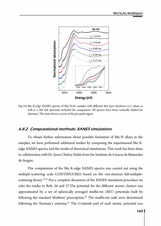
Mn/Si3N4 Multilayers
163
6540 6560 6580 6600
6534 6536 6538 6540 6542
Nor
mal
ized
abs
orpt
ion
Energy (eV)
Mn foil
tm= 7.6 nm
tm= 3.8 nm
tm= 0.86 nm
tm= 0.28 nm
tm= 0.17 nm
Fig. 6.8 Mn K-edge XANES spectra of Mn/Si3N4 samples with different Mn layer thickness (tm) values as
well as a Mn foil spectrum included for comparison. All spectra have been vertically shifted for clearness. The inset shows a zoom of the pre-peak region.
6.8.2. Computational methods: XANES simulations
To obtain further information about possible formation of Mn-N alloys in the
samples, we have performed additional studies by comparing the experimental Mn K-
edge XANES spectra and the results of theoretical simulations. This work has been done
in collaboration with Dr. Jesus Chaboy Nalda from the Instituto de Ciencia de Materiales
de Aragón.
The computation of the Mn K-edge XANES spectra was carried out using the
multiple-scattering code CONTINUUM23 based on the one-electron full-multiple-
scattering theory.24,25 For a complete discussion of the XANES simulation procedure we
refer the reader to Refs. 26 and 27.The potential for the different atomic clusters was
approximated by a set of spherically averaged muffin-tin (MT) potentials built by
following the standard Mattheis’ prescription.28 The muffin-tin radii were determined
following the Norman’s criterion.29 The Coulomb part of each atomic potential was

CChhaapptteerr 66
generated using charge densities obtained from a non-local self-consistent Dirac-Fock
code.30,31 The atomic orbitals were chosen to be neutral for the ground state potential,
whereas different choices were used to build the final state potential and we have found
during the present calculations that the screened and relaxed Z+1 option32 lead to the
best performance for the simulation of the experimental absorption spectra at the Mn K-
edge. The calculated theoretical spectra have been further convoluted with a Lorentzian
shape function to account for the core-hole lifetime33 (Γ = 1.2 eV) and the experimental
resolution (Γ = 1 eV).
It should be noted that despite the current progress in XANES computation
several problems, as the treatment of the inelastic losses of the photoelectron, still
remains an open problem.34 By this reason we have started the computation on a
reference material, metallic α-Mn, in order to fix the main parameters of the calculations.
The first step of the calculations was deserved to determine the size of the cluster
needed to reproduce all the spectral features present in the experimental XANES spectra.
To this end we have performed the computation of the Mn K-edge XANES in the case of
α-Mn (I-43m) by increasing progressively the number of atoms in the cluster. It should
be noted that because Mn occupies four different crystallographic positions 2a (Mn1), 8c
(Mn2), 24f (Mn3), 24g (Mn4) XANES computations have to be performed for four
different clusters in which the absorbing Mn atom lies at the different Mni sites, being the
theoretical spectrum made up from the weighted sum of these contributions according
the crystallographic statistical ratio. In this way, we have determined that the
computations performed for clusters including contributions from neighboring atoms
located within the first 7 Å around photoabsorbing Mn account for all the observed
spectral features, and the addition of further coordination shells does not contribute
significantly to the XANES spectrum. We have also studied the effect of both the
maximum angular momentum quantum number, lmax, and the overlapping factor
imposed to the muffin-tin spheres to build up the potential into reproducing the Mn K-
edge XANES spectrum. We have found that the best reproduction of the experimental
spectrum is obtained by using lmax = 4 and a 1% overlapping factor to build up a 7 Å

Mn/Si3N4 Multilayers
165
cluster. The results of these computations are shown in Fig. 6.9(a). The agreement
between the computations and the experimental signal is noticeable as the calculations
reproduce the step-like profile at the threshold (A), the main peak (B) and the two
structures located at 28 (C) and 47 eV (D) above the edge. During the calculations we
have tested the performance of the energy dependent Hedin-Lundqvist (HL) and Dirac-
Hara (DH) exchange and correlation potentials (ECP) potentials. Moreover, we have
also made computations by using only the real part of the HL ECP (hereafter, real HL)
and, in addition, we have built a ”complex” DH one by adding to it the imaginary part of
the HL one. As shown in Fig. 6.9(a), the performance of the different EPC potentials is
similar although in the case of the HL the calculated absorption maxima falling short of
the observed ones. By contrast, computations performed by using the DH ECP show a
better reproduction of the relative energy position among the peaks. This is evidenced by
the reproduction of the main resonance D and the negative dip E located, respectively, at
47 eV and 62 eV above the edge. Moreover, the addition of the imaginary part of the HL
potential improves the calculations yielding the use of the complex DH ECP the best
reproduction of the intensity ratio among the different spectral features.i
Possessing these results we have further performed the computation of the Mn K-
edge spectrum in the case of both θ-MnN (Mn Oh environment) and η-Mn3N2 (Mn in
two different environments: fivefold pyramids and linear twofold coordination with a
ration of 2:1).
In the case of MnN, computations have been performed for a cluster containing
179 atoms that includes all the contributions from neighbouring atoms located within
the first 7.4 Å around the absorbing Mn atom. In the case of Mn3N2, Mn occupies two
different crystallographic sites 2a (Mn1) and 4e (Mn2). Hence, XANES computations
have been performed for two clusters in which the absorbing Mn atom lies at the
different Mn1 and Mn2 sites. These clusters include the scattering contributions within
the first 7.5 Å around the absorber and contain 153 and 150 atoms for Mn1 and Mn2,
respectively. The Mn K-edge absorption of Mn3N2 has been calculated by adding the i It should be noted that the assessment of the quality of the theoretical computations is based on the correct reproduction of the shape and energy position of the different spectral features and of their relative energy separation and intensity ratio as well.

CChhaapptteerr 66
theoretical computations obtained for both clusters according the crystallographic
statistical ratio.
The results of these computations are compared to the experimental spectrum of
the tm = 0.28 nm sample in Fig. 6.9(b). The computed spectra show similar oscillations in
the high energy region. However, their spectral profiles at the threshold region differ,
especially concerning the pre-edge peak (A). This peak is experimentally observed and
typically assigned to a non-centrosymmetric environment of the absorbing site, such as in
tetrahedral coordination (Td) symmetry. The theoretical simulation reproduces this
peak for η-Mn3N2, while it is absent for MnN. These results suggesting the presence of
η-Mn3N2 in our samples have been verified by studying the modification of the XANES
spectra as a function of the thickness.
Indeed, as the Mn thickness increases the η-Mn3N2 contribution should be
hindered as the XANES would be made by the superposition of the XANES spectra of
both η-Mn3N2 and bulk-Mn-like. This is shown in Fig. 6.9(c) where the XANES spectra
of the samples with different Mn thickness (tm) are compared to the theoretical spectra
calculated as the weighted addition of the computed spectra for η-Mn3N2 and α-Mn in
the form: n x Mn3N2 + m x α-Mn. As shown in the figure, the modification of the Mn
thickness strongly changes the spectral profile in the high energy region. For example, in
the case of the sample with the small Mn thickness (tm = 0.28 nm) the spectrum shows a
negative dip (D) at ∼ 33 eV above the edge. As the Mn thickness increases, samples tm =
3.8 nm and tm = 7.6 nm, this spectral feature evolves up to yield a positive resonance. This
is exactly the situation obtained in the theoretical simulation of Fig. 6.9(c): whereas the
Mn3N2 dominates the spectrum, feature D remains negative but, however, as the
contribution of bulk Mn increases, the sign of this contribution is reversed. Similar
analysis can be followed for the energy position of the main resonance E at ∼ 57 eV above
the edge.

Mn/Si3N4 Multilayers
167
0.0
0.5
1.0
0.0
0.5
1.0
1.5
-50 -25 0 25 50 75 100 125 1500.0
0.5
1.0
Rmax = 7 Å
Mn K-edge(a)
real HL
complex Dirac-Hara
HL
Dirac-Hara
FEDCB
A
tm= 0.28 nm
complex Dirac-Hara
Mn3N2
MnNNor
mal
ised
Abs
. (ar
b. u
nits
)
(b)
0.000
0.025
0.050
0.075
Theoretical Com
putation (arb. units)
DE
A
B
C
tm= 7.6 nm
tm= 3.8 nm
tm= 0.28 nm
ED
C
B
A
Mn-foil-like
E - E0 (eV)
(c)
0.000
0.025
0.050
n Mn3N2
α-Mn0%25%50%
75%100%
n x Mn3N2 + m x α-Mn
0.000
0.025
0.050
Fig. 6.9 (a) Comparison between the Mn K-edge of a Mn metallic foil (●) and the theoretical spectra
calculated on a 7 Å cluster by using lmax = 4 and different ECP potentials: real HL (blue, dots), real DH (green, dash line), complex HL (black, solid line) and complex DH (purple, dot-dash). (b) Comparison between the experimental Mn K-edge XANES of the tm = 0.28 nm Mn sample (●) and the theoretical computation performed for both MnN (blue, dots) and Mn3N2 (red, solid line) by using the complex Dirac-Hara ECP potential. (c) Comparison between the experimental Mn K-edge XANES of the tm = 0.28 nm (black, ●), tm = 3.8 nm (green, □) and tm = 7.6 nm (red, ○) samples and the theoretical signals calculated as the weighted sum of the computed spectra for both Mn3N2 and α-Mn (see text for details) as a function of the Mn3N2 fraction n: 100 % (cyan, solid line), 75% (black, dots), 50% (red, dash), 25% (blue, dot-dash) and 0% (green, ○).

CChhaapptteerr 66
Experimentally, this feature is shifted towards higher energies as the Mn thickness
increases in the samples, in identical manner to the behaviour of the theoretical signal
constructed by varying the weight of the η-Mn3N2 and α-Mn contribution to the XANES
spectra. The obtained evolution agrees with the [Mn]/[Mn3N2] ratio obtained by RBS
and XPS.
Therefore, the ab-initio calculations have evidenced the presence of both
metallic and Mn3N2 phase (with non-centrosymmetric Mn symmetry) in sample tm
= 7.6 nm, while no sign of Mn metallic phase appears in the tm = 0.28 nm spectrum,
which presents just nitride contribution. The [Mn metal]/[Mn3N2] ratio indicated by
XANES simulations for sample tm = 7.6 nm is compatible with the previous one
estimated by XPS and EXAFS (about 3:2 of metal/nitride). The fact that increasing the
Mn-layer thickness lead to a reduction of the relative contribution of η-Mn3N2 compared
to the bulk-like Mn indicates that the Mn nitride formation in the sputtered Mn layer is
related to the Si3N4 interfaces, leading, for thin enough Mn layers, to all the deposited Mn
turned into manganese nitride.
6.8.3. Extended X-Ray Absorption Fine Structure (EXAFS)
Further confirmation of these results has been obtained by studying the Mn local
environment from the analysis of the EXAFS part of the spectra by using the VIPER
software.35 Additional details of the analysis procedure are given in section 2.6.1.2.
Figure 6.10 shows the evolution of the Fourier transform (FT) magnitude of the
EXAFS signal at the Mn K-edge along the series with tm variable and a Mn metal foil,
given for comparison. At first glance, clear differences between the FT magnitude of the
tm = 7.6 nm sample and the others, as well as the loss of the FT second peak for small tm values, are observed.

Mn/Si3N4 Multilayers
169
0 2 4 6 8
FT [k
2 χ(k)
]
Distance (Å)
tm = 7.6 nm
tm = 3.8 nm
tm = 0.86 nm
tm = 0.5 nm
tm = 0.17 nm
Fig. 6.10 Experimental EXAFS Fourier Transforms (FT) of some representative [Mn(tm)/Si3N4(3nm)]n
samples.
The comparison between experimental data and simulations is shown in Fig. 6.11,
and the obtained results are summarized in Table 6.III. Analysis shows a complex
situation that can be explained as follows. A contribution around 2.05 Å corresponding
to Mn-N distance is present for all the samples from the series and besides, samples
with tm higher than 0.5 nm present a second Mn-Mn near 3 Å. Those distances agree
with Mn3N2 compounds with slightly compressed distances.8 Additionally, a small
Mn-Si contribution at about 3.1 Å has been found for tm = 0.86 nm and tm = 3.8 nm
samples, what can be assigned to the link between the Mn3N2 and Si3N4 phases. Finally,
the Mn-Mn distance found at 2.67 Å in sample tm = 7.6 nm is in agreement with
distances in metallic Mn. The expected small size of Mn3N2 clusters explains the
disappearance of the FT second peak for tm ≤ 0.5 nm and does not allow to obtain Mn-
Mn and Mn-Si distances for these samples. In the case of the tm = 7.6 nm sample, EXAFS
results are in agreement with previous XANES conclusions. For this sample, significant
presence of metallic Mn (with Mn-Mn distances widely spread around 2.7 Å) is found;
this additional phase as well as the small number of layers make very hard to obtain the
minority Mn-Si contribution.
At this point, it is important to note that the observation of this Mn-Si EXAFS
distance supports the fact that Mn3N2 phase is formed at the interface between the Mn

CChhaapptteerr 66
and Si3N4 layers, suggesting that the Si3N4 has a definitive influence in the development
of a strained Mn3N2 phase. Within the error in the neighbor number determination, the
Mn metal/Mn3N2 ratio obtained by EXAFS is compatible with the one extracted by both
XPS and XANES data (4:3).
0 1 2 3 4
2 3 4 5 6 7 8 9 10
FT
[k2 χ(
k)]
Distance (Å)
tm= 7.6 nm
(b)
tm= 3.8 nm
tm= 0.86 nm
tm= 0.5 nm
tm= 0.17 nm
k2 χ(
k)
Wavenumber (Å-1)
tm= 7.6 nm
(a)
tm= 3.8 nm
tm= 0.86 nm
tm= 0.5 nm
tm= 0.17 nm
Fig. 6.11 (a) k-space comparison between the filtered EXAFS signals (dots) and simulations (lines) at Mn
K-edge of samples with different Mn layer thickness (tm). (b) Fourier transform of the (a) plotted signals; modulus and imaginary parts have been presented for dual comparison with calculated contributions (lines).

Mn/Si3N4 Multilayers
171
Table 6.III. EXAFS results summary: atomic distance (R), number of neighbors (N) and Debye-Waller factor (σ2).
Sample pair R
(Å) N
σ2
(× 10-3Å2)
[Mn(tm)/Si3N4(3.4nm)]n tm = 7.6 nm Mn−N
Mn−Mn
Mn−Mn
2.03±0.02
2.67±0.02
2.98±0.02
2.4±1
4.2±1
6.0±1
5±1
25±1
29±1
tm = 3.8 nm Mn−N
Mn−Mn
Mn−Si
2.06±0.02
3.06±0.02
3.12±0.02
3.1±1
3.4±1
2.3±1
9±1
17±1
7±1
tm = 0.86 nm Mn−N
Mn−Mn
Mn−Si
2.04±0.02
2.98±0.02
3.10±0.02
2.6±1
2.8±1
1.1±1
7±1
7±1
9±1
tm = 0.5 nm Mn−N 2.02±0.02 2.9±1 12±1
tm = 0.28 nm Mn−N 2.06±0.02 3.1±1 22±1
tm = 0.17 nm Mn−N 2.04±0.02 2.7±1 8±1
[Mn(0.7nm)/Si3N4(tsn)]43 tsn = 6.7 nm Mn−N 2.04±0.02 2.9±1 10±1
tsn = 1.0 nm Mn−N 2.03±0.02 3.2±1 6±1
By contrast, no appreciable Mn metal contribution is obtained from the EXAFS
analysis of the tm = 3.8 nm sample. In comparison with the other samples, slightly higher Mn-
Mn distances (3.06 Å) are found in the Mn3N2 phase of the tm = 3.8 nm sample, being one of
the most ferromagnetic ones. Results from EXAFS simulations of samples with different
Si3N4 layer thickness (Fig. 6.12) are included in Table 6.III. As expected, similar Mn-N
distances are obtained when varying tsn. It can be observed that the change in the atomic
environment when varying tsn is smaller than the resulting when modifying tm, where larger
magnetization values were found. Just very small differences are detected by EXAFS for the

CChhaapptteerr 66
samples with different tsn values.
0 1 2 3 4
2 3 4 5 6 7 8 9
FT [k
2 χ(k)
]
Distance (Å)
tsn= 6.7 nm
(b)
tsn= 1.0 nm
k2 χ(
k)
Wavenumber (Å-1)
tsn= 6.7 nm
(a)
tsn= 1.0 nm
Fig. 6.12 (a) k-space comparison between the filtered EXAFS signal (dots) and simulations (lines) at Mn
K-edge of samples with different Si3N4 layer thickness (tsn). (b) Fourier transform of the (a) plotted signals; modulus and imaginary parts have been presented for dual comparison with calculated contributions (lines).
6.8.4. XAS at the Mn L3,2-edge and XMCD
Additional XAS and XMCD experiments at the Mn L3,2 edge have been carried out
since they become of great interest here. On one hand, the Mn L3,2 XAS structure is a
fingerprint for the 3d count, giving information on the Mn valence state and on the other
hand, XMCD provides an element-specific tool sensitive to the magnetic states. Further
information of these techniques can be found in section 2.6.3.
Mn L3,2 edge XAS and XMCD measurements were done on beamline 5U.1 of the
Synchrotron Radiation Source at Daresbury Laboratory (UK) in collaboration with Dr.
Neil Telling and Prof. Gerrit Van Der Laan.

Mn/Si3N4 Multilayers
173
Spectra were collected in TEY mode reversing the applied magnetic field of ±0.6 T
perpendicular to the surface at each data point for fixed photon helicity. Figure 6.13
shows the XAS and XMCD spectra of the tm = 0.28 nm sample measured at RT.
Comparison of the experimental XAS spectrum with theoretical calculations for different
electronic configurations indicates that the 3dn → 2p53dn+1 absorption spectrum
corresponds to a Mn2+ d5 ground state. For further information, theoretical simulations
performed by G. Van der Laan et al. 36 of the 2p absorption spectra of the Mn 3d3, Mn 3d4
and Mn 3d5 in tetrahedral (Td) and octahedral (Oh) symmetry are shown in Fig 2.3
(section 2.6.2). The obtained results sustain a non-centrosymmetric Td Mn environment
with a crystal field close to 10Dq ≈ 0.5 eV, in agreement with the above XANES and
EXAFS results.
Fig. 6.13 Mn L3,2 XAS and XMCD spectra of [Mn(0.28nm)/Si3N4(3.4nm)]75 sample measured at RT
compared to XAS calculations for Mn d5 in Td symmetry. The L3 and L2 step edges have been subtracted from the experimental XAS spectrum.
The difference between the XAS spectra recorded for parallel and antiparallel
alignment of magnetic field and photon helicity results in a small XMCD signal for the tm
= 0.28 nm sample. Reversal of the XMCD signal was confirmed by switching between left
and right circular polarization. A seven-points smooth of the dichroic signal is shown in
Fig. 6.14, in comparison with the d5 calculation. The XCMD signal shows that the

CChhaapptteerr 66
magnetism arises from a Mn d5 contribution (Mn2+), which has its largest value at the
photon energy position of the XAS peak maximum.
Fig. 6.14 Comparison between Mn XMCD spectrum of [Mn(0.28nm)/Si3N4(3.4nm)]75 sample measured
at RT and calculations for Mn d5 in Td symmetry.
6.9. Remarks and discussion
The combined results allow us to deduce how the Mn2+ cations bonded to
nitrogen lead to FM order and what the role is of the silicon-nitride matrix. Firstly,
ferromagnetism caused by Mn metallic clusters can be clearly ruled out by XMCD
results. Furthermore, FM due to formation of ternary phases, such as MnSiN2,37 seems
quite doubtful due to the silicon film content extracted from the RBS measurements. On
the other hand, substitution of Si4+ by Mn2+ in Si3N4 seems rather unlikely due to the
difference in ionic radii and considerable charge mismatch. Si sites are four-fold
coordinated in Si3N4, with Si-N distances of ~1.74 Å. The Mn2+ ionic radius (0.80 Å) in
Td symmetry greatly differs from the Si4+ radius (0.40 Å). Large lattice distortions, which
could accomplish a reduction of the coordination number and relieve the possible charge
mismatch, might be considered. Even though, the large Mn-N distances (2.05 Å),
obtained by EXAFS hardly match with the Mn2+ replacement in Si3N4. Therefore, FM

Mn/Si3N4 Multilayers
175
due to Mn2+ substitution into the Si3N4 matrix can be also ruled out.
Significant contribution from manganese nitrides such as ε-Mn4N, ζ-Mn2N, or ζ-Mn5N2 phases, can be rejected due to the large dissimilarity in the Mn-N atomic distance.
Therefore, all the obtained results points towards induced ferromagnetism in the
Mn3N2 stabilized phase evidenced by XANES and EXAFS results at the Mn K-edge, with
a manganese oxidation state of +2.
The situation seems very similar to the theoretically reported ferromagnetism in a
distorted θ-MnN phase. This compound has a tetragonally distorted rocksalt structure,
where Mn has octahedral (Oh) symmetry and a Mn-N distance of 2.098 Å,9 with an AF
ground state.2 However, depending on the polymorph and lattice constant, theoretical
calculations have predicted FM order, e.g., in the zinc-blende structure, which would
exhibit shorter Mn-N distances and Mn Td symmetry. In fact, the θ-MnN compound has
a tendency to lose nitrogen, forming the η-Mn3N2 phase which presents similar Mn-N
distances.8
In the case of Mn/Si3N4 films, the Mn-N distances of 2.05 Å obtained by EXAFS
are slightly shorter than the average in η-Mn3N2 (2.1 Å), where Mn is coordinated by
fivefold nitrogen pyramids. Hence, taking into consideration the changes in the unit cell
volume commonly considered for accounting for theoretical transitions to a FM phase
with Mn in Td symmetry from the AFM ground state in manganese nitrides, 6,11,12 the
obtained results suggest that the origin of the FM behaviour in Mn/Si3N4 multilayers is
the formation of a slightly distorted non-centrosymetric η-Mn3N2 phase at the
interfaces, what seems to be favored by the Si3N4 tetrahedral structure.
Regarding all the obtained results, the evolution of MS within the multilayer series
can be qualitatively understood.
For samples with Mn-rich layers smaller than 0.86 nm, mostly Mn2+ contribution
was obtained by XPS, being this Mn2+ average oxidation state corroborated by XANES
measurements at the Mn K-edge. The Mn3N2 phase formation has been verified by
EXAFS and XANES simulations. EXAFS results have shown the disappearance of the
second neighbour shell for these samples, indicating the presence of Mn3N2 clusters of

CChh
sm
th
nm
ho
of
th
EX
th
pe
no
in
fer
XM
Fig
we
no
all
M
hhaapptteerr 66
mall size. The d
he superparamag
m. Looking at th
ow the superpar
On the oth
f both, metallic M
he Mn3N2 forma
XAFS results an
hrough the form
er Mn atom.
A scheme
oticed that min
stance) can com
rromagnetism
MCD.
g. 6.15 Simplified Mn metal aMn3N2 laye
In order to
e have calculate
ormalizing only
l the Mn atoms
Mn atom at RT,
ecrease of the m
gnetic size limi
he hysteresis lo
ramagnetic com
her hand, for lar
Mn and Mn2+, h
ation, favoured b
nd XANES calc
mation of the me
of the situatio
nor contribution
mplicate this im
in this system
structural image oand Mn3N2 phases ers is expected.
o estimate the r
ed the effective s
to the Mn com
s (previously co
being closer to
magnetization f
it, which becom
ops at low temp
mponent become
rge Mn-rich laye
have been foun
by the surround
culations. In this
etallic Mn phas
on described is
ns from possibl
mage. However, i
has been ascr
of multilayer samplcoexist and (b) wit
reduction of the
saturation magn
ming from Mn3N
nsidered in Fig
the maximum
for these sample
mes important f
perature (cf Fig
es significant as
er thickness sam
nd by XPS. The
ded Si3N4, have
s case, the redu
se that reduces t
s represented in
e additional ph
it is important t
ribed to Mn d5
les (a) with higher th tm < 0.86 nm, wh
e MS due to the
netization at RT
N2 (about 30 % f
g. 6.5(c)). This
value of Ms wi
es is explained
for particle size
g. 6.5(a)) it can
tm is reduced.
mples, major co
metallic Mn pr
e been corrobor
uction of MS is u
the specific ma
n Fig. 6.15. It
hases (MnN or
o remark that th5 contribution
Mn layer thickneshere formation of d
e presence of m
T of sample tm =
from XPS data)
leads to about 0
thin the series,
in terms of
es around 1
be noticed
ntributions
resence and
ated by the
understood
gnetization
should be
Mn4N, for
he origin of
(Mn2+) by
ss (tm), where discontinuons
metallic Mn,
= 7.6 nm by
), instead of
0.23 μB per
about 0.35
Mn/Si3N4 Multilayers
177
μB per Mn atom. Another factor, like small differences in the lattice parameters (Mn-Mn
distances larger than 3 Å were found for the tm = 3.8 nm sample) seems to be directly
related to variations in the FM order established in the Mn3N2 distorted phase. The role
of the Si3N4 layer thickness in the ferromagnetism has been also evidenced in the
[Mn(0.7nm)/Si3N4(tsn)]43 series, even if higher MS values and stronger variation were
obtained when varying the Mn layer thickness (tm). The stabilization of the
ferromagnetic Mn3N2 distorted phase results favored when both, the manganese-rich and
the silicon nitride layers are comparable in thickness, where slightly larger Mn-Mn
distances were found. This point is consistent with the fact of finding Mn-Si EXAFS
contribution in samples with intermediate tm, what evidences a clear relationship
between the Mn3N2 distorted phase and the surrounded Si3N4 for these similar
thicknesses, where the imprinted stresses seem to promote the stabilization of the Mn3N2
distorted phase.
6.10. Conclusions
The magnetic, structural and electronic properties of Mn/Si3N4 multilayer
samples prepared by reactive sputtering have been investigated using SQUID, XRR,
TEM, RBS, NRA, XPS, XAS, and XMCD.
RTFM has been obtained in Mn/Si3N4 multilayer samples with different
Mn:Si3N4 relative ratio for the first time.
XMCD has shown that the magnetism in the films is due to the Mn d5 (Mn2+)
state and XANES calculations have confirmed the presence of a Mn3N2 phase with Mn
Td symmetry, what seems to be favored by the Si3N4 tetrahedral structure.
The origin of ferromagnetism here has been assign to the formation of a distorted
non-centrosymmetric Mn3N2 phase with slightly shorter Mn-N distances. This type of
changes in the unit cell volume has been commonly theoretically considered in order to
obtain transitions from the AFM ground state to a FM phase in manganese nitrides.
An evolution of the magnetic properties has been found depending on the Mn and

CChhaapptteerr 66
Si3N4 layer thickness. The variation of the ferromagnetic component has been explained
in terms of the Mn3N2 phase.
For small Mn layer thickness, in the cluster growth regime, the Mn3N2 clusters size
limits the magnetization magnitude, leading to a decrease of Ms as the cluster size is
reduced.
By contrast, for thicker Mn layer thickness samples, the formation of metallic Mn
phase results in diminishing the magnetization per Mn atom. The coexistence of metallic
Mn and manganese nitride has been deduced by XPS, XAS and XANES calculations.
The most suitable condition found here to stabilize the ferromagnetic ordering in
this system seems when the manganese and silicon nitride layers are continuous and their
thickness are comparable and close to 3.5 nm. Several factors as, small differences in the
atomic distances, contributions from possible additional phases (MnN or Mn4N, for
instance) or the inherent instability of the formed phase can lead to more complicated
magnetic behaviours.

Mn/Si3N4 Multilayers
179
ADDITIONAL INFORMATION
The most common polymorphs of crystalline Si3N4 are the α phase (P3/m) and
the β phase (P63/m) which is the most stable one, both with hexagonal crystal structures.
The unit cell of the α- Si3N4 phase, with a = 7.753 Å and c = 5.618 Å, contains four
formula units (28 atoms), while the β-Si3N4 phase, with a = 7.606 Å and c= 2.909 Å,
contains two formula units (14 atoms). The main difference between both structures lays
in the stack arrangement. The Si3N4 structure can be described as a stacking of Si-N
layers in the (001) direction, in an ABCD ABCD sequence for the α-Si3N4 phase, while in
an ABAB sequence for the β-Si3N4 phase.
Figure 6.16 shows a ball-stick model of β-Si3N4. All Si atoms are equivalent (6h sites), but there are two inequivalent nitrogen sites: N(2c) at 2c sites and N(6h) at 6h sites. The N(2c) atoms are in a planar geometry with their three Si nearest neighbors,
and the N(6h) atoms are in slightly puckered sites surrounded by three Si atoms,
whereas Si atoms are at the center of slightly irregular tetrahedron bonded with one
N(2c) atom and three N(6h) atoms.38
Fig. 6.16. A ball-stick model of β-Si3N4. The green, red and blue spheres represent Si atoms at 6h sites, N
atoms at 2c sites, N atoms at 6h sites, respectively. N atoms are within the same plane of their three nearest neighbours, whereas Si atoms lie at the center of a slightly irregular.
Si3N4 thin films prepared by sputtering have been previously studied by Dr.
Mercedes Vila. More information about Si3N4 can be found in her Doctoral Thesis.39 In
particular, Si3N4 films prepared by reactive sputtering from Si with pure nitrogen (as
described in Chapter 6) exhibit no trace of oxygen and amorphous character.
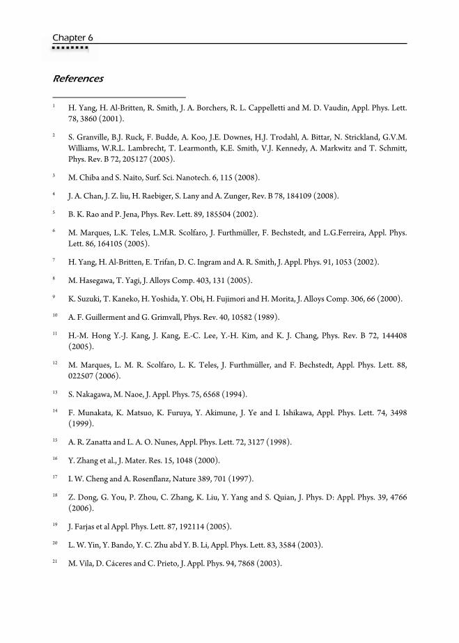
CChhaapptteerr 66
References
1 H. Yang, H. Al-Britten, R. Smith, J. A. Borchers, R. L. Cappelletti and M. D. Vaudin, Appl. Phys. Lett.
78, 3860 (2001).
2 S. Granville, B.J. Ruck, F. Budde, A. Koo, J.E. Downes, H.J. Trodahl, A. Bittar, N. Strickland, G.V.M. Williams, W.R.L. Lambrecht, T. Learmonth, K.E. Smith, V.J. Kennedy, A. Markwitz and T. Schmitt, Phys. Rev. B 72, 205127 (2005).
3 M. Chiba and S. Naito, Surf. Sci. Nanotech. 6, 115 (2008).
4 J. A. Chan, J. Z. liu, H. Raebiger, S. Lany and A. Zunger, Rev. B 78, 184109 (2008).
5 B. K. Rao and P. Jena, Phys. Rev. Lett. 89, 185504 (2002).
6 M. Marques, L.K. Teles, L.M.R. Scolfaro, J. Furthmüller, F. Bechstedt, and L.G.Ferreira, Appl. Phys. Lett. 86, 164105 (2005).
7 H. Yang, H. Al-Britten, E. Trifan, D. C. Ingram and A. R. Smith, J. Appl. Phys. 91, 1053 (2002).
8 M. Hasegawa, T. Yagi, J. Alloys Comp. 403, 131 (2005).
9 K. Suzuki, T. Kaneko, H. Yoshida, Y. Obi, H. Fujimori and H. Morita, J. Alloys Comp. 306, 66 (2000).
10 A. F. Guillerment and G. Grimvall, Phys. Rev. 40, 10582 (1989).
11 H.-M. Hong Y.-J. Kang, J. Kang, E.-C. Lee, Y.-H. Kim, and K. J. Chang, Phys. Rev. B 72, 144408 (2005).
12 M. Marques, L. M. R. Scolfaro, L. K. Teles, J. Furthmüller, and F. Bechstedt, Appl. Phys. Lett. 88, 022507 (2006).
13 S. Nakagawa, M. Naoe, J. Appl. Phys. 75, 6568 (1994).
14 F. Munakata, K. Matsuo, K. Furuya, Y. Akimune, J. Ye and I. Ishikawa, Appl. Phys. Lett. 74, 3498 (1999).
15 A. R. Zanatta and L. A. O. Nunes, Appl. Phys. Lett. 72, 3127 (1998).
16 Y. Zhang et al., J. Mater. Res. 15, 1048 (2000).
17 I. W. Cheng and A. Rosenflanz, Nature 389, 701 (1997).
18 Z. Dong, G. You, P. Zhou, C. Zhang, K. Liu, Y. Yang and S. Quian, J. Phys. D: Appl. Phys. 39, 4766 (2006).
19 J. Farjas et al Appl. Phys. Lett. 87, 192114 (2005).
20 L. W. Yin, Y. Bando, Y. C. Zhu abd Y. B. Li, Appl. Phys. Lett. 83, 3584 (2003).
21 M. Vila, D. Cáceres and C. Prieto, J. Appl. Phys. 94, 7868 (2003).

Mn/Si3N4 Multilayers
181
22 M. Vila, E. Román and C. Prieto, J. Appl. Phys. 97, 113710 (2005).
23 C. R. Natoli and M. Benfatto (unpublished).
24 P. A. Lee and J. B. Pendry, Phys. Rev. B 11, 2795 (1975).
25 C. R. Natoli and M. Benfatto, J. Phys. (Paris) Colloq. 47, C8-11 (1986).
26 See for example J. Chaboy and S. Quartieri, Phys. Rev. B 52, 6349 (1995) and references therein.
27 C. R. Natoli, M. Benfatto, S. Della Longa and K. Hatada, J. Synchrotron Rad. 10, 26 (2003).
28 L. F. Mattheis, Phys. Rev. A 133, 1399 (1964); Phys. Rev. A 134, 970 (1964).
29 J. G. Norman, Mol. Phys. 81, 1191 (1974).
30 A. L. Ankudinov, B. Ravel, J. J. Rehr and S. D. Conradson, Phys. Rev. B 58, 7565 (1998).
31 J. P. Desclaux, Comp Phys Comm. 9, 31 (1975).
32 P. A. Lee and G. Beni, Phys. Rev. B 15, 2862 (1977).
33 M. O. Krause and J. H. Oliver, J. Phys. Chem. Ref. Data 8, 329 (1979).
34 J. Chaboy, J. Synchrotron Rad. 16, 533 (2009).
35 K. V. Klementiev, VIPER for Windows, freeware: www.desy.de/∼klmn/viper.html; J. Phys. D. 34, 209 (2001).
36 G. van der Laan and I. W. Kirkman, J. Phys.: Condens. Matter 4, 4189 (1992).
37 S. Esmaeilzadeh, U. Hålenius and M. Valldor, Chem. Mat. 18, 2713 (2006).
38 Y. Cai, L. Zhang, Q. Zeng, L. Cheng and Y. Xu, Phys. Rev. B 74, 174301 (2006).
39 M. Vila Juárez, Doctoral Thesis “Nitruro de silicio: de la lámina delgada a las uniones cerámicas” (UAM, ICMM-CSIC, 2003).


183
The study of noble metal nanoparticles embedded in ceramic matrices shown here
is the result of an international scientific stay at the Laboratoire de Chimie Physique
(LCP) at the University of Paris-Sud, in France, under the supervision of Dr. Agnès
Traverse, who conceived this research project.
The increasing scientific interest on noble metal nanoparticles systems added to
the acquired experience of the research group in Si3N4 and ZnO films as well as in
sequential deposition of metal/ceramic material by sputtering, has prompted us to
complete this thesis based on the ferromagnetism in wide band gap materials with the
study of NPs embedded in wide band gap matrices. The multiple possibilities of these
multifunctional materials are therefore highlighted here.
C.1. Au/Si3N4 Multilayers
C1.1. Motivation
Metallic nanoparticles (NPs) are of great interest in chemistry,1,2 medical
sciences3,4 or material sciences.1,5,6 As a consequence of reducing the size and the
dimensionality of a material, its density of states changes drastically as the spatial length
scale of the electronic motion is reduced.7,8,9 The energy eigenstates are determined by
the system’s boundaries, and therefore, surface effects become very important. For that
reason, NPs of subnanometer to nanometer size present exciting properties which are
strongly different from those of bulk materials. As a result, possible future applications of
NPs include the areas of ultrafast data communication and optical data storage,5 solar
energy conversion,6 and the use of metallic NPs as catalysts due to their high surface-to-
volume ratios.5
AAppppeennddiixx CC
From Ferromagnetism to Noble Metal Nanoparticles Formation in the Si3N4 and ZnO Systems

AAppppeennddiixx CC
In particular, noble metal NPs exhibit surface plasmon resonance (SPR)
phenomenon when excited at an appropriate wavelength, usually located in the visible
range. These are pronounced resonance lines in the optical spectra caused by collective
excitations of conduction electrons, induced by the interacting electromagnetic field.1
The optical properties are known to be controlled by a variety of effects. Specifically, the
SPR spectral position depends on the NP metal; for instance, silver NPs generally have
higher particle-plasmon energies than gold NPs.1,10 The spectral position also depends
on the size, shape and organization of NPs.11,12
It is possible to incorporate NPs within ceramic matrices in order to form
composite materials. These materials, called nanocermets, exhibit additional properties
particularly interesting for applications in linear and non-linear regimes. One can
mention the existence of a strong absorption band, second13 and third-order nonlinear
susceptibility14,15 and a femtosecond response16 that make them potential candidates for
the realization of optoelectronic components.
The refractive index of the matrix is known to play an important influence on the
SPR energy. In general, increasing the refractive index of the surrounding medium leads
to an enhancement of the plasmon band intensity and bandwidth as well as to a red shift
of the resonance energy.9 Regarding the ceramic matrix, significant research has been
done already on Au NPs embedded in oxide matrices such as SiO2 and TiO2.17
A precise characterization of these nanocermets from the structural point of view
is a prerequisite to fully interpret their properties. In this work, we present a study of the
Au NPs growth and optical properties in the transparent nitride Si3N4, with a refractive
index of 2, intermediate between the one of SiO2 (1.5) and TiO2 (2.7).
Au NPs inside Si3N4 matrix have been prepared here by sequential sputtering of
Au and Si3N4. Among the techniques to prepare embedded metal NPs, alternative
sputtering allows the experimentalists to vary parameters such as the total amount of
deposited material, the layer thickness and deposition rate in order to monitor NP
growth.12 The control of the growth mode together with NP size, morphology and

From Ferromagnetism to Noble Metal Nanoparticles Formation in the Si3N4 and ZnO Systems
185
organization are of fundamental importance to prepare samples with the optimised
optical properties. For that reason, thorough structural characterizations to understand
growth mechanisms are essential here.
In this appendix, a structural and optical characterization of a series of Au/Si3N4
samples is presented. Several experimental techniques have been combined to determine
the growth mode and to provide a fine description of the Au NPs in terms of average size,
size distribution, morphology and organization in the matrix.
C.1.2. Preparation of samples
Au/Si3N4 multilayered films were prepared by sequential sputtering of Si3N4 and
Au on Si(100) substrates at room temperature. The residual pressure was near 1x10⁻⁷
mbar. Si3N4 layers were deposited by RF sputtering from a pure silicon target (99.999%)
using N2 as reactive sputtering gas at a pressure of 6.0x10⁻³ mbar. The deposition rate was
about 4 nm/min for a RF power of 100 W. Au layers were grown from a Au target
(99.999%) at 5.0x10⁻³ mbar pressure of pure Ar. The deposition rate was about 5
nm/min for a DC power of ~10 W. Pre-sputtering was developed before multilayer
growth and also between two consecutive layers. The sequence of deposition was always
started and finished with a Si3N4 layer so Au grows always on the same type of surface
and becomes protected against atmospheric contamination.
Following the described procedure, a series of five Au/Si3N4 samples, labelled as
[Si3N4(70s)/Au(t-sput)]n was prepared. Whereas the Si3N4 sputtering time per layer was
maintained constant in every sample, the Au layer sputtering time (t-sput) was varied
between 88 s and 7 s. The expected Si3N4 layer thickness is therefore approximately
constant in every sample (about 6 nm) while the expected Au layer thickness (tAu) ranges
from 8 to 1 nm. The number of bilayers (n) was increased in order to maintain the Au
total amount approximately constant in the five samples. The prepared samples are
summarized in Table C.1.I. Calculated effective thickness of samples has been included
in the table, where for all samples (either formed by continuous or discontinuous Au-

AAppppeennddiixx CC
layers) the effective Au-layer thickness has been obtained from the Au bulk density (ρAu
= 5.9x10²² at/cm3) considering hypothetical Au continuous layers formed by the same
Au amount as if present as NPs.
Table C.1.I Sample series description: sputtering time for the Si3N4 and Au-layer deposition and number
of bilayers (n), XRR-obtained bilayer thickness (XRR-Λ), GISAXS-obtained bilayer thickness (GISAXS-Λ), number of Au atoms per Au-layer measured by RBS (at/cm2), calculated effective Au-layer thickness (tAu) using RBS data and Au metal bulk density (ρAu = 5.9x10²² at/cm3), total number of Si atoms measured by RBS (at/cm2) and sample effective thickness values considering RBS-tAu and the Si3N4-layer thickness average among all the samples, from Λ and tAu.
Sample [Si3N4(70s)/Au(t-sput)]n
XRR-Λ
(nm)
GISAXS-Λ
(nm)
RBS Au atoms per layer (at./cm2)
RBS tAu
(nm)
RBS total Si atoms (at./cm2)
Sample effective thickness
[Si3N4(70s)/Au(88s)]5 13.2 14.0 4.9x10¹⁶ 8.3 3.7x10¹⁶ [Si3N4(6nm)/Au(8.3nm)]5
[Si3N4(70s)/Au(44s)]10 8.5 - 2.75x10¹⁶ 4.7 9.3x10¹⁶ [Si3N4(6nm)/Au(4.7nm)]10
[Si3N4(70s)/Au(22s)]20 10.4 9.8 1.73x10¹⁶ 2.9 2.7x10¹⁷ [Si3N4(6nm)/Au(2.9nm)]20
[Si3N4(70s)/Au(11s)]40 8.6 - 1.26x10¹⁶ 2.1 5.0x10¹⁷ [Si3N4(6nm)/Au(2.1nm)]40
[Si3N4(70s)/Au(7s)]75 6.7 7.7 9.4x10¹⁵ 1.6 9.4x10¹⁷ [Si3N4(6nm)/Au(1.6nm)]75
C.1.3. X-Ray Reflectivity (XRR)
The XRR curves of the Au/Si3N4 samples, measured with a Bruker D8 X-ray
diffractometer with a Cu Kα source at the ICMM facilities, are shown in Fig. C.1.1.
Maxima corresponding to heterostructure periodicity can be observed for all samples,
indicating that films are actually formed by alternated Si3N4 and Au-rich regions, leading
to out-of-plane periodicity. It should be noted in the figure that the spectra of samples
with shortest bilayer numbers, named as [Si3N4(70s)/Au(88s)]5 and [Si3N4(70s)/Au(44s)]10,
also exhibit the short oscillations corresponding to finite size film interferences, not
appearing for the other samples due their large thickness, which overpass the XRR

From Ferromagnetism to Noble Metal Nanoparticles Formation in the Si3N4 and ZnO Systems
187
thickness measurement range. In the particular case of [Si3N4(70s)/Au(88s)]5 sample,
maxima coming from bilayer period together with the total film thickness peaks lead to
less pronounced maxima and a slightly different spectrum. The effect of the extra Si3N4
layer deposited on top, more noticeable for this thinnest sample, makes more complex
the spectral shape.
1 2 3 4 5 6 7
[Si3N4(70s)/Au(7s)]75
[Si3N4 70s)/Au(11s)]40
[Si3N4(70s)/Au(22s)]20
[Si3N4(70s)/Au(44s)]10
[Si3N4(70s)/Au(88s)]5
Inte
nsity
2θ (°)
Fig. C.1.1 X-ray Reflectivity (XRR) spectra of the Si3N4/Au sample series. Curves have been vertically shifted for clearness.
Calculated bilayer thickness values from the XRR spectra analysis are shown in
Table C.1.I (XRR-Λ). It can be noticed that the bilayer thickness obtained for
[Si3N4(70s)/Au(44s)]10 sample (Λ = 8.5 nm) is very closed to the one found for
[Si3N4(70s)/Au(11s)]40 sample (Λ = 8.6 nm). Moreover, [Si3N4(70s)/Au(22s)]20 sample shows
Λ = 10.4 nm, which is larger than the 8.5 nm obtained for [Si3N4( 70s)/Au(44s)]10 sample,
prepared with double Au deposition time. It should be taken into account that these
differences are too big to be ascribed to uncertainties in the Λ magnitude. Furthermore,
considerably similar Λ values have been found by both XRR and GISAXS experiments
(see Table C.1.I), with completely different experimental set-up.
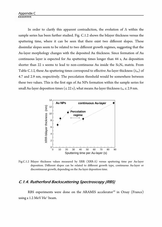
AAppppeennddiixx CC
In order to clarify this apparent contradiction, the evolution of Λ within the
sample series has been further studied. Fig. C.1.2 shows the bilayer thickness versus the
sputtering time, where it can be seen that there exist two different slopes. These
dissimilar slopes seem to be related to two different growth regimes, suggesting that the
Au-layer morphology changes with the deposited Au thickness. Since formation of Au
continuous layer is expected for Au sputtering times longer than 44 s, Au deposition
shorter than 22 s seems to lead to non-continuous Au inside the Si3N4 matrix. From
Table C.1.I, these Au sputtering times correspond to effective Au-layer thickness (tAu) of
4.7 and 2.9 nm, respectively. The percolation threshold would be somewhere between
these two values. This is the first sign of Au NPs formation within the sample series for
small Au-layer deposition times (≤ 22 s), what means Au-layer thickness tAu ≤ 2.9 nm.
0 10 20 30 40 50 60 70 80 900
2
4
6
8
10
12
14
Percolationregime
XRR
-bila
yer t
hick
ness
(nm
)
Sputtering time per Au-layer (s)
Au NPs continuous Au-layer
Fig.C.1.2 Bilayer thickness values measured by XRR (XRR-Λ) versus sputtering time per Au-layer
deposition. Different slopes can be related to different growth type, continuous Au-layer or discontinuous growth, depending on the Au-layer deposition time.
C.1.4. Rutherford Backscattering Spectroscopy (RBS)
RBS experiments were done on the ARAMIS accelerator18 in Orsay (France)
using a 1.2 MeV He+ beam.
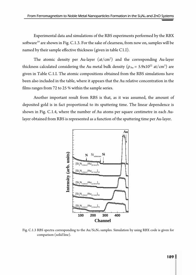
From Ferromagnetism to Noble Metal Nanoparticles Formation in the Si3N4 and ZnO Systems
189
Experimental data and simulations of the RBS experiments performed by the RBX
software19 are shown in Fig. C.1.3. For the sake of clearness, from now on, samples will be
named by their sample effective thickness (given in table C1.I).
The atomic density per Au-layer (at/cm2) and the corresponding Au-layer
thickness calculated considering the Au metal bulk density (ρAu = 5.9x10²² at/cm3) are
given in Table C.1.I. The atomic compositions obtained from the RBS simulations have
been also included in the table, where it appears that the Au relative concentration in the
films ranges from 72 to 25 % within the sample series.
Another important result from RBS is that, as it was assumed, the amount of
deposited gold is in fact proportional to its sputtering time. The linear dependence is
shown in Fig. C.1.4, where the number of Au atoms per square centimetre in each Au-
layer obtained from RBS is represented as a function of the sputtering time per Au-layer.
100 200 300 400
Inte
nsity
(arb
. uni
ts)
Channel
Au
SiN
[Si3N4 (6nm)/Au(8.3nm)]5
[Si3N4 (6nm)/Au(4.7nm)]10
[Si3N4 (6nm)/Au(2.9nm)]20
[Si3N4 (6nm)/Au(2.1nm)]40
[Si3N4 (6nm)/Au(1.6nm)]75
Sisubstrate
Fig. C.1.3 RBS spectra corresponding to the Au/Si3N4 samples. Simulation by using RBX code is given for
comparison (solid line).
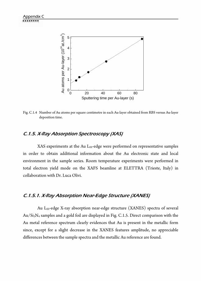
AAppppeennddiixx CC
0 20 40 60 800
1
2
3
4
5
Au
atom
s pe
r Au-
laye
r (10
16at
./cm
2 )
Sputtering time per Au-layer (s)
Fig. C.1.4 Number of Au atoms per square centimetre in each Au-layer obtained from RBS versus Au-layer deposition time.
C.1.5. X-Ray Absorption Spectroscopy (XAS)
XAS experiments at the Au LIII-edge were performed on representative samples
in order to obtain additional information about the Au electronic state and local
environment in the sample series. Room temperature experiments were performed in
total electron yield mode on the XAFS beamline at ELETTRA (Trieste, Italy) in
collaboration with Dr. Luca Olivi.
C.1.5.1. X-Ray Absorption Near-Edge Structure (XANES)
Au LIII-edge X-ray absorption near-edge structure (XANES) spectra of several
Au/Si3N4 samples and a gold foil are displayed in Fig. C.1.5. Direct comparison with the
Au metal reference spectrum clearly evidences that Au is present in the metallic form
since, except for a slight decrease in the XANES features amplitude, no appreciable
differences between the sample spectra and the metallic Au reference are found.

From Ferromagnetism to Noble Metal Nanoparticles Formation in the Si3N4 and ZnO Systems
191
11900 11925 11950 11975 12000
Nor
mal
ized
Abs
orpt
ion
[Si3N4 (6nm)/Au(1.6nm)]75
[Si3N4 (6nm)/Au(2.1nm)]40
[Si3N4 (6nm)/Au(2.9nm)]20
Energy (eV)
Au metal foilAu L-edge
Fig.C.1.5. XANES of several samples in comparison with the Au metal reference spectra. C.1.5.2. Extended X-Ray Absorption Fine Structure (EXAFS)
EXAFS analysis was performed using the standard procedure described in section
2.6.1.2. Simulations of the experimental data for three representative samples and a
standard Au metal foil can be observed in Fig. C.1.6. Pairs and distances obtained from
the data analysis are summarized in Table C.1.II.
Table. C.1.II Au atomic surrounding given by EXAFS analysis. R, N and σ2 correspond to the atomic distance, number of neighbours and Debye-Waller factor, respectively.
Sample
Au-Au
R (Å)
N σ2 (10-3Å2)
Au foil 2.85±0.01 11.5±0.5 8.9±0.5 [Si3N4(6nm)/Au(8.3nm)]5 2.85±0.01 10.5±1.0 9.5±1.0 [Si3N4(6nm)/Au(2.9nm)]20 2.84±0.01 10.4±0.5 9.7±0.5 [Si3N4(6nm)/Au(2.1nm)]40 2.84±0.01 10.2±0.5 9.8±0.5

AAppppeennddiixx CC
0 1 2 3 4 5
3 4 5 6 7 8 9 10 11 12 13 14
tAu = 2.1 nm
F T
[k2 χ(
k))]
Distance (Å)
tAu = 8.3 nm
tAu = 2.9 nm
(b)
Au foil
tAu = 2.1 nm
tAu = 2.9 nm
tAu = 8.3 nm
Au foil
k2 χ(k)
Wavenumber (Å-1)
(a)
Fig. C.1.6 (a) k-space comparison between the experimental EXAFS signal (dots) and simulations (lines) at Au L-edge of samples tAu = 8.3, 2.9, 2.1 nm and a Au foil. (b) Fourier transform of the (a) plotted signals; modulus and imaginary parts are shown for dual comparison with the simulated contributions (lines).
It can be observed that the Au-Au distances obtained for each sample, about 2.85
Å, coincide with the Au metal reference. Considering additional Au-N or Au-Si
contributions in the simulations is not necessary since Au-Au simulations reproduce the
experimental data. Therefore, possible Au/Si3N4 interdiffusion in the samples is too
small to be detected. The EXAFS results clearly indicate Au metal formation, either as
continuous layer or as NPs, in all the sample series. However, it should be noted that the
decrease of tAu entails a slight decrease of the Au-Au coordination number N and a slight

From Ferromagnetism to Noble Metal Nanoparticles Formation in the Si3N4 and ZnO Systems
193
increase of the amplitude loss factor σ2. Moreover, it appears that for tAu = 8.3 nm, the N
value is strongly dependent on the σ2 value. An uncertainty in the Au coordination
number of the order of ± 1 is thus expected here whereas it is of ± 0.5 for the other samples.
It can be noted that the fact that the Au-Au distance obtained by EXAFS for each
sample agrees with the Au metal reference value (about 2.85 Å) supports the above
consideration of the Au bulk density (ρAu = 5.9x10²² at/cm3) for the calculation of the
effective Au-layer thickness in these samples.
C.1.6. Grazing Incidence Small Angle X-ray Scattering (GISAXS)
More precise information about the Au morphology and NP dimensions was
obtained by GISAXS measurements, carried out on the SWING beamline at SOLEIL
synchrotron (France) in collaboration with Dr. David Babonneau and Dr. Olivier Lyon.
The energy of the incident X-ray beam was set at 9.03 keV (λ = 0.137 nm), the
angle of incidence was slightly higher than θc in order to achieve good surface sensitivity,
and the sample-to-detector distance was varied between 1.305 and 2.425 m. The
transmitted and specularly reflected beams were masked by a vertical beam-stop and the
scattered intensity was collected as a function of the in-plane (2θf) and out-of-plane (αf)
exit angles with a 2D charge-coupled device (CCD) detector. The experimental data
were analysed with the FitGISAXS package developed within the IGOR Pro analysis
software (WaveMetrics, Inc.) by David Babonneau.
The 2D GISAXS patterns of the samples with tAu = 8.3 nm, 2.9 nm and 1.6 nm are
shown in Fig. C.1.7.
For tAu = 8.3 nm, only Bragg peaks characteristics of a rough multilayer20 can be
seen in the vicinity of the vertical beam-stop (Fig. C.1.7a). Thus the presence of isolated
NP is unlikely. A vertical cut at 2θf = 0.32° showing 5 Bragg peaks with a q-period of
about 0.45 nm-1 (Fig. C.1.7b) enables the period of the multilayer to be estimated as
Λ = 14.0 nm, quite in agreement with the period of 13.2 nm determined by XRR.

AAppppeennddiixx CC
For tAu = 2.9 nm, in addition to Bragg peaks indicating layering with a q-period of
about 0.64 nm-1 corresponding to Λ = 9.8 nm (also in agreement with the value
determined by XRR). The pattern presents typical features of a distribution of isolated
NP with in-plane spatial correlation indicating that short-range order has taken place
(Fig. C.1.7c). The quantitative analysis of the GISAXS intensity within the distorted
wave Born approximation21 was performed on the basis of a horizontal cut at αf = 0.19°
using the local monodisperse approximation22 and assuming spherical NPs with no
vertical correlation between NPs (i.e., each layer has a morphology which is completely
independent from the adjacent layers.23,24 As seen in Fig. C.1.7d, the experimental data
are well reproduced with a Gaussian size distribution of NPs with an average diameter
φ = 6.9 nm, a full width at half maximum of 3.2 nm, and an interparticle distance of
9.6 nm.
For tAu = 1.6 nm, the pattern is typical of a distribution of isolated NPs without
spatial correlation (Fig. C.1.7e). The horizontal cut at αf = 0.29° (symbols) and fit (red
line) taking into account spheres with a Gaussian size distribution leads to an average
diameter φ = 5.1 nm with a full width at half maximum of 2.1 nm (Fig. C.1.7f). A vertical
cut at 2θf = 0.32° showing 2 Bragg peaks gives a q-period of about 0.82 nm-1
corresponding to Λ = 7.7 nm close to 6.7 nm as found by XRR.
The bilayer thicknesses and NP sizes measured with the GISAXS technique are
given in Table C.1.I and in Table C.1.III, respectively. Also given in Table C.1.III are the
average diameters determined from XRD measurements of the (111) Au reflection (not
shown) by using the Scherrer formula. It can be seen that the agreement between these
φ values and those determined by GISAXS is quite good. The areal NP density given in
Table C.1.III is equal to the number of Au atoms per square centimetre in each Au-layer
(obtained by RBS) divided by the number of atoms per NP (obtained from the volume
calculated with the diameter, φ, measured by GISAXS and considering the Au bulk
density of 5.9x10²² at/cm3). Estimated average interparticle distance (L) has been also
included in the table.

From Ferromagnetism to Noble Metal Nanoparticles Formation in the Si3N4 and ZnO Systems
195
Fig. C.1.7 2D GISAXS patterns of [Si3N4(6nm)/Au(t)]n multilayers for (a) tAu= 8.3 nm, (c) tAu = 2.9 nm, (e)
tAu = 1.6 nm, (b) vertical cut for tAu = 8.3 nm (2θf = 0.32º) and (d) and (f) horizontal cuts for tAu = 2.9 nm (αf = 0.19º) and tAu = 1.6 nm (αf = 0.29º), respectively.
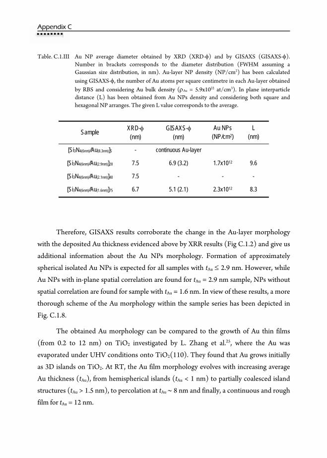
AAppppeennddiixx CC
Table. C.1.III Au NP average diameter obtained by XRD (XRD-φ) and by GISAXS (GISAXS-φ). Number in brackets corresponds to the diameter distribution (FWHM assuming a Gaussian size distribution, in nm). Au-layer NP density (NP/cm2) has been calculated using GISAXS-φ, the number of Au atoms per square centimetre in each Au-layer obtained by RBS and considering Au bulk density (ρAu = 5.9x10²² at/cm3). In plane interparticle distance (L) has been obtained from Au NPs density and considering both square and hexagonal NP arranges. The given L value corresponds to the average.
Sample XRD-φ (nm)
GISAXS-φ (nm)
Au NPs (NP/cm2)
L (nm)
[Si3N4(6nm)/Au(8.3nm)]5 - continuous Au-layer
[Si3N4(6nm)/Au(2.9nm)]20 7.5 6.9 (3.2) 1.7x10¹² 9.6
[Si3N4(6nm)/Au(2.1nm)]40 7.5 - - -
[Si3N4(6nm)/Au(1.6nm)]75 6.7 5.1 (2.1) 2.3x10¹² 8.3
Therefore, GISAXS results corroborate the change in the Au-layer morphology
with the deposited Au thickness evidenced above by XRR results (Fig C.1.2) and give us
additional information about the Au NPs morphology. Formation of approximately
spherical isolated Au NPs is expected for all samples with tAu ≤ 2.9 nm. However, while
Au NPs with in-plane spatial correlation are found for tAu = 2.9 nm sample, NPs without
spatial correlation are found for sample with tAu = 1.6 nm. In view of these results, a more
thorough scheme of the Au morphology within the sample series has been depicted in
Fig. C.1.8.
The obtained Au morphology can be compared to the growth of Au thin films
(from 0.2 to 12 nm) on TiO2 investigated by L. Zhang et al.25, where the Au was
evaporated under UHV conditions onto TiO2(110). They found that Au grows initially
as 3D islands on TiO2. At RT, the Au film morphology evolves with increasing average
Au thickness (tAu), from hemispherical islands (tAu < 1 nm) to partially coalesced island
structures (tAu > 1.5 nm), to percolation at tAu ∼ 8 nm and finally, a continuous and rough
film for tAu = 12 nm.
From Ferromagnetism to Noble Metal Nanoparticles Formation in the Si3N4 and ZnO Systems
197
Fig. C.1.8 Bilayer thickness values (averaged XRR-Λ and GISAXS-Λ) versus the number of Au atoms per square centimetre in each Au-layer measured by RBS. Au continuous layers are obtained for Au-layer atomic densities ≥ 2.75 x 10¹⁶ at/cm2 (tAu ≥ 4.7 nm) leading to Si3N4/Au multilayered samples. For Au-layer atomic density = 1.73 x 10¹⁶ at/cm2 (tAu = 2.9 nm), Au NPs with short-range order are obtained while no in-plane correlation is obtained for the smallest Au-layer atomic density, 9.4 x 10¹⁵ at/cm2 (tAu = 1.6 nm).
In addition, they found that the inter-island distance reaches a saturation value
after deposition of 1.5 nm average thickness of Au (close to 10 nm) and remains constant
afterwards. In our case of sequential deposition, it has been obtained similar growth type
and percolation values between tAu of 2.9 and 4.7 nm, which are smaller but comparables
to those reported ones.
Further details of the different Au NPs distribution can be observed in Fig. C.1.9,
where structural parameter obtained by GISAXS and XRR for tAu = 1.6 nm (Fig.
C.1.9(a)) and tAu = 2.9 nm (Fig. C.1.9(b)) samples are shown for comparison. The
differences found in the average diameter values in comparison with nominal values (for
example, φ = 5.1 nm for tAu = 1.6 nm) were similarly found in Ag NPs embedded in Si3N4
prepared by ion beam sputtering, where NPs of 6 nm of average height were found for
nominal tAg = 1 nm.12

AApp
ap
in
be
go
stu
Fig
C.
op
ex
wa
sp
Au
ha
ppppeennddiixx CC
It can be
pproximately by
-plane interpart
eing close to the
old thickness of
udied samples.
g. C.1.9 SchematitAu = 2.9 obtained
C.1.7. UV-VIS
Au NPs sa
ptical absorptio
xperimental con
ay. The optical
pectrophotomet
Fig. C.1.10
u NP samples w
as been included
observed in Fi
y 3/2 of φ distan
ticle distance (L
e saturation valu
1.5 nm. By con
ic comparison betwnm. NP average di
d by GISAXS and X
S Absorption
amples were add
n in transmissio
nditions as the a
l absorption of
ter at the ICMM
0 shows the opt
with tAu = 1.6 nm
d for compariso
ig C.1.9, for in
nce in both case
L) and out-of-p
ue of 10 nm rep
ntrast, we have n
ween Au NPs moriameter (φ), interp
XRR.
n
ditionally grown
on mode. Thes
above-described
f these films w
M, in the 200–90
ical absorption
m and tAu = 2.9
on. SPR wavelen
stance, that NP
es. For each sam
plane periodicit
ported by L. Zh
not reached a sat
rphology for samplparticle distance (L
n on quartz sub
se samples were
d multilayers to
was measured w
00 nm ultraviole
coefficient as a
nm. Optical ab
ngth is about 57
Ps are separate
mple, the obtain
ty (Λ) have sim
hang et al.25 for a
turation value fo
le with (a) tAu = 1.6L) and bilayer thick
bstrates to meas
e prepared unde
be compared i
with a Cary 40
et-visible range.
function of wav
sorption from a
70 nm for tAu =
ed in plane
ned average
milar values,
an effective
for L for the
6 nm and (b) kness (Λ) are
sure sample
er identical
in the same
000 UV-vis
velength of
a Si3N4 film
1.6 nm and

From Ferromagnetism to Noble Metal Nanoparticles Formation in the Si3N4 and ZnO Systems
199
587 nm for tAu = 2.9 nm samples. Note that the SPR of tAu = 2.9 nm slightly redshifts. This
fact is in agreement with theory and experiments for nanoparticles much smaller than the
wavelength of the absorbing light (where dipole approximation is valid, φ < 25 nm for
gold), which predict that the maximum of the SPR clearly red shifts with increasing Au
volume fraction.9
200 300 400 500 600 700 800 900
Abs
orpt
ion
Coe
ffici
ent (
cm-1)
Wavelength (nm)
Si3N4 film
tAu = 2.9 nm
tAu
= 1.6 nm
Fig. C.1.10 Optical absorption coefficient of Au NP samples with tAu = 2.9 (φ = 6.9 nm) and tAu = 1.6 nm (φ = 5.1 nm). A sputtered Si3N4 film is presented for comparison. Absorption has been normalized to total sample thickness.
In Fig. C.1.11, sample optical spectra have been qualitatively compared to the
Maxwell-Garnett (M-G) effective medium model just by considering Au bulk optical
properties and a volume fraction (f) equal to 29% for the case of tAu = 2.9 nm and 22% for
tAu = 1.6 nm (calculated from RBS data). In M-G theory, εeff satisfies the equation.26,27
m
m
meff
meff fεε
εεεε
εε22 +
−=
+
− (C.1.1)
Where ε is the dielectric function of the metallic particles and εm is the dielectric
function of the matrix. The dielectric function of Au has been taken from Palik database

AAppppeennddiixx CC
and the medium dielectric function εm is taken as a constant of 4 for the Si3N4. The
absorption coefficient of the composite can be obtained from the following formula27
( )[ ] 2/1
12/12
2212
4eee εεε
λπα −+= (C.1.2)
Here εe1 and εe2 are the real and imaginary parts of the effective dielectric function εeff.
Compared to theory, slightly red-shifts are obtained for the two experimental SPR.
200 300 400 500 600 700 800 900
M-G Sim (f = 0.29; εm= 4) M-G Sim (f = 0.22; ε
m= 4)
Wavelength (nm)
tAu = 2.9 nm
tAu = 1.6 nm
Fig. C.1.11 Optical absorption coefficient of Au NP samples with tAu = 2.9 (φ = 6.9 nm) and tAu = 1.6 nm (φ = 5.1 nm) compared to Maxwell-Garnet (M-G) theory using f = 0.29 and f = 0.22 (calculated from RBS data of tAu = 2.9 and tAu = 1.6 nm, respectively), Au bulk optical properties and the dielectric function of Si3N4 (εm = 4).
Apart from the dielectric properties of the cluster metal, it has been mentioned
that the SPR spectral position depends on the size, shape and NPs organization, as well as
on the surrounding medium. Therefore, there are different factors that can explain these
small deviations from expected values. For the sake of clarity, we have discussed here
these factor for two cases: i) the case of quasi-static regime, for what only the dipole term
is assumed to contribute to the absorption (for gold, it happens for Au NPs with φ < 25

From Ferromagnetism to Noble Metal Nanoparticles Formation in the Si3N4 and ZnO Systems
201
nm, which is our experimental situation) and where changes in the spectra are therefore
referred to as intrinsic size effects as well as for ii) the non quasi-state case (φ > 25 nm),
that is, in the extrinsic size region, where the dipole approximation is not valid.
Considering the surrounding medium, an increase of the refractive index of the
Si3N4 matrix can induce a SPR red-shift.1,9,28 However, this fact does not seem to explain
the observed red-shift. M-G calculation has been done considering a matrix refractive
index approximately equal to the Si3N4 bulk value of 2. Taking that into consideration,
smaller index in comparison with the bulk material might be expected in our samples, but
not an enhancement.
On the other hand, the size effect of the plasmon absorption does not result so
evident. While for Au NPs with φ > 25 nm (extrinsic size region) the peak position shifts
to longer wavelengths as higher order multipole terms increasingly dominate,29 the
situation is more complicated for smaller NPs, for which intrinsic size effects should
dominate. Experimentally, both a blue shift and a red shift of the SPR have been found
when decreasing size.1,9 Furthermore, the magnitude of the wavelength shift in the
absorption maximum for NPs in the intrinsic size region is usually small compared to the
total line width of the plasmon resonance. The SPR peak position is therefore, usually
not as well suited for a discussion of a size effect within the quasi-static regime.
By contrast, much more drastic effect on the surface plasmon absorption is found
if the NP shape is changed. Assuming deviation from spherical shape (typically
spheroidal NPs with a revolution axis perpendicular to the substrate and H/D axis ratio,
which is commonly observed, for instance in Ag NPs embedded in Si3N4)12,28, a decrease
of the H/D axis ratio (oblate-like shape) can also induce a SPR red-shift. A little
ellipsoidal deformation of the mainly spherical Au NPs can explain the small difference
between theory and experimental data in the SPR position of these samples.
If we consider now the plasmon bandwidth, for the case of large Au particles (φ >
25 nm), it is well known that the SPR bandwidth increases with increasing size. When the
wavelength becomes comparable to the dimension of the NP, it leads to an
inhomogeneous polarization of the NP by the electromagnetic field. The broadening of

AAppppeennddiixx CC
the SPR is usually ascribed to retardation effects, as well as the excitation of different
multipole modes, with peaks at different wavelengths.1,9,29
For the case of smaller Au NPs, the SPR bandwidth is size-independent within the
dipole approximation. However, a size effect on the SPR has been experimentally
observed as the plasmon bandwidth increases with decreasing particle size. In fact, it is
quite well established that the bandwidth is inversely proportional to the radius of the
particle for sizes smaller than 20 nm.1,9 Nevertheless, we have found similar bandwidths
for both samples (FWHM of about 200 nm), being a bit larger for the tAu = 2.9 nm
sample than for the tAu = 1.6 nm one (with smaller NP size), contrary to reported results.
Even so, a broadening of the size distribution of the NPs is also expected to induce
a broadening of their size shape distribution. Since cluster shape is known to influence
the spectral position of the SPR, such a size-induced broadening of their shape
distribution may result in a broadening and maybe a spectral shift of the SPR band.28
From this point of view, the broader NP size distribution found for tAu = 2.9 nm sample in
comparison with tAu = 1.6 nm (see FWHM of φ distribution, in Table. C.1.III) might be
associated with a slightly broader SPR for tAu = 2.9 nm in Fig. C.1.10. For these samples,
the SPR width seems more dependent of size distribution than of NPs arrange.
In view of these results, the SPR spectral position of Au NPs embedded in Si3N4
seems to be mainly modified by the Au volume fraction, which is varied along the sample
series. The effect of the surrounding medium appears similar for both samples, with a
matrix refractive experimental index close to 2.0. A slightly deviation from spherical
shape for the Au NPs (oblate-like shape) may explained the small red shift observed in
the SPR of both samples in comparison with M-G mean field theory. In addition, the
larger NP size distribution in tAu = 2.9 nm can explain its slightly broader SPR.
From Ferromagnetism to Noble Metal Nanoparticles Formation in the Si3N4 and ZnO Systems
203
C.1.8 Conclusions
With the aim of growing Au NPs inside Si3N4 matrix in a controlled way, a series of
Au/Si3N4 samples has been prepared by sequential sputtering technique, keeping
constant the Si3N4 layer thickness and modifying the effective Au layer thickness (tAu).
A change in the Au-layer morphology with the deposited Au amount has been
evidenced by XRR and GISAXS results. While continuous Au layers leading to
multilayered samples have been found for tAu ≥ 4.7 nm, non-continuous Au-layers
resulting in Au NPs inside the Si3N4 matrix have been found for tAu ≤ 2.9 nm, being the
percolation regime between these values. Approximately spherical isolated Au NPs with
average sizes ranging between 7- 5 nm and a size distribution with FWHM of 40-45%
have been obtained. The Au NP density is of the order of 1012 NP/cm2.
Moreover, different Au NP distributions depending on the Au-layer thickness
have been evidenced by GISAXS. While Au NPs (φ = 7 nm) with in-plane spatial
correlation are found for tAu = 2.9 nm sample, Au NPs (φ = 5 nm) without spatial
correlation are found for the smallest Au-layer sample, with tAu = 1.6 nm.
For both samples, UV-vis absorption spectrum shows a surface plasmon resonance
(SPR) effect, revealing that, despite of its stratified character, both samples can be
considered as homogeneous films in terms of their optical response.
Within the series of NPs samples, the SPR spectral position, which is the main
characteristic of the nanocomposite optical properties, is mainly determined by the Au
volume fraction, which is varied along the sample series, and the nature of the
surrounding material, which is the same for all samples. In agreement with theory, the
SPR shifts towards longer wavelengths with increasing the Au-layer effective thickness
(and consequently the Au volume fraction).
A slightly deviation from spherical shape for the Au NPs (oblate-like spheroids)
may explain the small red shift observed in the SPR of these samples in comparison with
Maxwell-Garnet theory. In addition, the larger NP size distribution in tAu = 2.9 nm

AAppppeennddiixx CC
sample (φ = 7 nm) can explain its slightly broader SPR in comparison with tAu = 1.6 nm
sample (φ = 5 nm).
The obtained dependence of the SPR maximum on the effective Au-layer
thickness makes this system tunable for optical applications requiring a specific
absorption spectrum.

From Ferromagnetism to Noble Metal Nanoparticles Formation in the Si3N4 and ZnO Systems
205
References
1 U. Kreibig and M Vollmer, Optical Properties of Metal Cluster (Berlin: Springer) Vol 25 1995.
2 C. R. Henry Surf. Sci. Rep. 31, 232 (1998).
3 T. Schalkammer, A. Leitner, F. R. Aussenegg, G. Bauer and F. Pittner, SPIE Proc.3253, 12 (1998).
4 V. P. Zharov, E. N. Galitovskaya, C. Johnson and T. Kelly, Lasers Surg. Med. 37, 219 (2005).
5 G. Schmid, Clusters and Colloids: From Theory to Application; (VCH: Weinheim) 1994.
6 M. Graetzel, Electrochemistry in Colloids and Dispersions; Ed. R. A. Mackay, J. Texter; (VCH: Weinheim, New York) 1992.
7 A. Henglein, J. Phys. Chem. 97, 8457 (1993).
8 A. P. Alivisatos, J. Phys. Chem. 100, 13226 (1996).
9 S. Link and M. A. El-Sayed, J. Phys. Chem. B103, 8410 (1999).
10 C. Sönnichsen, T Franzl, T Wilk, G. von Plessen and J Feldmann, New J. Phys. 4, 93.1-93.8 (2002).
11 J. Tourdert, D. Babonneau, L. Simonot, S. Camelio and T. Girardeau, Nanotechnology 19, 125709 (2008).
12 T. Girardeau, S. Camelio, D. Babonneau, J. Tourdert, A. Barranco, Thin Solid Films 313, 455 (2004).
13 D. Ricard, P. Roussignol, C. Flytzanis, Opt. Lett. 10, 511(1985).
14 M. Breit, V. A. Podolskiy, S. Grésillon, G. von Plessen, J. Feldmann, J. C. Rivoal, P. Gadenne, Andrey K. Sarychev and Vladimir M. Shalaev Phys. Rev. B 64, 125106 (2001).
15 Jean-Michel Lamarre, Franck Billard, Chahineze Harkati Kerboua, Michel Lequime, Sjoerd Roorda, Ludvik Martinu, Optics Communications 281, 331(2008).
16 O. L. Muskens, N. Del Fatti and F. Vallée, Nano Lett. 6, 552 (2006).
17 L. Arlemao, D. Barreca, G. Bottaro, A. Gasparotto, S. Gross, C. Maragno, E. Tondello, Coordination Chemistry Reviews 250, 1294 (2006).
18 H. Bernas, J. Chaumont, E. Cottereau, R. Meunier, A. Traverse, C. Clerc, O. Kaitasov, F. Lalu, D. Le Du, G. Moroy and M. Salomé, Nucl Instr. and Meth. B 62, 416 (1992).
19 E. Kotai, Nucl. Instrum. Methods B 85, 588 (1994).

AAppppeennddiixx CC
20 V. Holý and T. Baumbach, Phys. Rev. B 49, 10668 (1994).
21 M. Rauscher, T. Salditt, and H. Spohn, Phys. Rev. B 52, 16855 (1995).
22 J.S. Pedersen, J. Appl. Crystallogr. 27, 595 (1994).
23 D. Babonneau, G. Abadias, J. Toudert, T. Girardeau, E. Fonda, J.-S. Micha, F. Petroff, J. Phys.: Condens. Mat. 20, 035218 (2008).
24 K. Salomon, O. Milat, M. Buljan, U.V. Desnica, N. Radić, P. Dubček, and S. Bernstorff, Thin Solid Films (to be published).
25 L. Zhang, F. Cosandey, R. Persaud and T. E. Madey, Surf. Sci. 439, 73 (1999).
26 B. Palpant, Phys. Rev B 57, 1963 (1998).
27 L. H. Zhou, C. H. Zhang, Y. T. Yang, B. S. Li, L. Q. Zhang, Y. C. Fu and H. H. Zhang, Nucl Instr. and Meth. B 267, 58 (2009).
28 J. Tourdert, S. Camelio, D. Babonneau, M-F Denanot and T. Girardeau, J. Appl Phys. 98, 114316 (2005).
29 G. C. Papavassiliou, Prog. Solid State Chem. 12, 185 (1980).

207
C.2. Au/ZnO Multilayers
C.2.1. Motivation
As it has been explained in Appendix C.1, the refractive index of the matrix plays
an important influence on the SPR.1,2 Motivated by the Au NPs growth obtained in the
transparent nitride Si3N4, with a refractive index of 2, we have performed a study of the
Au NPs growth in ZnO oxide matrix, which is also a material previously studied by the
research group and with refractive index close to 2. The aim of this work is therefore to
compare how Au NPs grow and arrange inside this other ceramic matrix, and the
corresponding influence on the optical properties of the nanocermet.
Similarly to the case of the Au/Si3N4 system, a detailed characterization of the
nanocermets from the structural point of view has been performed here to fully
understand their properties. In this Appendix, several experimental techniques have been
combined to determine the growth mode and to provide a description of the Au NPs in
terms of average size, morphology and organization in the matrix. The structural and
optical properties of this system have been compared to the ones obtained for the
Au/Si3N4 system.
C.2.2. Preparation of samples
Following the same procedure as the previously described for Au/Si3N4 samples
(Appendix C.1), Au/ZnO multilayered films were prepared by sequential sputtering of
AAppppeennddiixx CC
From Ferromagnetism to Noble Metal Nanoparticles Formation in the Si3N4 and ZnO Systems
AAppppeennddiixx CC
ZnO and Au on Si(100) and quartz substrates at room temperature. The residual
pressure was near 1x10⁻⁷ mbar. ZnO layers were deposited by reactive sputtering from a
pure Zn target (Goodfellow: 99.9%) using O2/Ar mixture gas (30% O2-rich) at a
working pressure of 5.4x10⁻³ mbar (the ZnO growth conditions are the same as the ones
used for Mn/ZnO series growth, described in Chapter 3). The deposition rate was about
3 nm/min for a DC power of ~5.5 W. Au layers were grown from a gold target
(99.999%) at 5.0x10⁻³ mbar pressure of pure Ar. The deposition rate was about 5
nm/min for a DC power of ~10 W. Pre-sputtering was developed before multilayer
growth and also between two consecutive layers. The sequence of deposition was always
started and finished with a ZnO layer so Au grows always on the same type of surface.
Following the above described method, a series of five Au/ZnO samples, labelled
as [ZnO(135s)/Au(t-sput)]n was prepared. Whereas the ZnO sputtering time per layer was
maintained constant in every sample, the Au layer sputtering time (t-sput) was varied
between 88 s and 7 s. The expected ZnO layer thickness is therefore approximately
constant in every sample (about 3 nm here) while the expected Au layer thickness (tAu)
ranges from 8 to 2 nm. The number of bilayers (n) was increased in order to maintain the
Au total amount approximately constant in the five samples. The prepared samples are
summarized in Table C.2.I, where the sputtering deposition time of the Au and ZnO
layers for each sample as well some structural and compositional parameters as bilayer
thickness (Λ) or number of atoms, obtained from XRR and RBS measurements, are
given.
In Table C.2.I, the labelled Au-layer “effective thickness” corresponds to the
calculated Au-layer thickness (tAu) using RBS and the Au bulk density (ρAu = 5.9x10²²
at/cm3) and similarly for the ZnO (RBS data and ρZnO = 8.3x10²² at/cm3). In the named
“sample effective thickness description”, it has been considered RBS-tAu and the ZnO-
layer thickness average among all the samples (from both XRR and RBS).
From now on, samples will be named by their sample effective thickness.

From Ferromagnetism to Noble Metal Nanoparticles Formation in the Si3N4 and ZnO Systems
209
Table C.2.I Sample series description: sputtering time for the ZnO and Au-layer deposition and number of bilayers (n), XRR-obtained bilayer thickness (XRR-Λ), RBS-obtained bilayer thickness (RBS-Λ), number of Au atoms per Au-layer and calculated effective Au-layer thickness (tAu), total number of Zn atoms measured by RBS (at/cm2) and calculated and ZnO-layer thickness (tZnO) using RBS data and bulk densities (ρAu = 5.9x10²² at/cm3 and ρZnO = 8.3x10²² at/cm3 respectively), sample effective thickness values considering RBS-tAu and the ZnO-layer thickness average among all the samples (from both XRR and RBS).
Sample [ZnO(135s)/Au(t-sput)]n
XRR-Λ
(nm)
RBS-Λ
(nm)
RBS Au-atoms per layer (at./cm2)
RBS tAu
(nm)
RBS total Zn-atoms (at./cm2)
RBS tZnO (nm)
Sample effective thickness
[ZnO(135s)/Au(88s)]5 10.5 11.1 4.60x10¹⁶ 7.8 6.1x10¹⁶ 3.3 [ZnO(3nm)/Au(7.8nm)]5
[ZnO(135s)/Au(44s)]10 7.5 7.6 2.71x10¹⁶ 4.6 1.0x10¹⁷ 3.0 [ZnO(3nm)/Au(4.6nm)]10
[ZnO(135s)/Au(22s)]20 6 6.2 2.12x10¹⁶ 3.6 4.4x10¹⁷ 2.6 [ZnO(3nm)/Au(3.6nm)]20
[ZnO(135s)/Au(11s)]40 5 5.8 1.41x10¹⁶ 2.4 1.1x10¹⁸ 3.4 [ZnO(3nm)/Au(2.4nm)]40
[ZnO(135s)/Au(7s)]75 5 5.8 1.06x10¹⁶ 1.8 2.5x10¹⁸ 4.0 [ZnO(3nm)/Au(1.8nm)]75
C.2.3. X-Ray Reflectivity (XRR)
The XRR curves of the Au/ZnO samples, measured with a Bruker D8 X-ray
diffractometer with a Cu Kα source at the ICMM facilities, are shown in Fig. C.2.1.
Maxima corresponding to heterostructure periodicity can be observed for all samples,
showing that films are actually formed by alternated ZnO and Au-rich regions, leading to
out-of-plane periodicity. In this case, short oscillations corresponding to finite size film
interferences are observed for [ZnO(3nm)/Au(7.8nm)]5, [ZnO(3nm)/Au(4.6nm)]10 and
[ZnO(3nm)/Au(3.6nm)]20 samples. In comparison with XRR spectra from [Si3N4(6nm)/Au(t)]n
samples (depicted in Fig. C.1.1), it seems that heterostructure peaks appear better
defined for these three Au/ZnO samples with n = 5, 10 and 20. By contrast, for samples
with smallest tAu values (n = 40 and 75), broader periodicity peaks are found for these
Au/ZnO samples in comparison with the others from the Au/ZnO series. Moreover, if
we compare [Si3N4(6nm)/Au(2.9nm)]40 and [ZnO(3nm)/Au(2.4nm)]40 sample spectra, a number
of three bilayer peaks can be clearly distinguished for the Au/Si3N4 sample, while only

AAppppeennddiixx CC
one is evidenced for Au/ZnO sample.
These results suggest that, for larger tAu values (tAu ≥ 3.6 nm) where formation of
continuous Au-layers is expected, sharper Au-ZnO interfaces in comparison with the Au-
Si3N4 ones are obtained. However, for small tAu values, where Au NP formation is
expected, out-of-plane periodicity gets worse for the Au/ZnO system compared to the
Au/Si3N4 one. Less well formed, or bad organized Au NPs inside ZnO are firstly evoked
by comparison of XRR measurements of both Au/ZnO and Au/Si3N4 systems.
1 2 3 4 5 6 7
[ZnO(3nm)/Au(1.8nm)]75
[ZnO(3nm)/Au(2.4nm)]40
[ZnO(3nm)/Au(3.6nm)]20
[ZnO(3nm)/Au(4.6nm)]10
[ZnO(3nm)/Au(7.8nm)]5
Inte
nsity
2θ (°)
Fig. C.2.1 X-ray Reflectivity (XRR) spectra of the Au/ZnO sample series. Curves have been vertically shifted for clearness.
The bilayer thickness values calculated from XRR spectra analysis (XRR-Λ) range
between 10.5 nm and 5 nm within the sample series (Table C.2.I). The evolution of the
experimental bilayer thickness obtained by XRR versus the Au-layer deposition time can
be seen in Fig. C.2.2. Differing from the Au/Si3N4 case, XRR-Λ exhibits approximately
linear variation with the Au-layer sputtering time for all the sample series. A change in the
Au-layer morphology cannot be related here to the existence of two different slopes
within this sample series. It seems that for this system, Au-layer continuous growth is
preserved until shorter Au-layer sputtering times than in the case of Au/Si3N4 samples.

From Ferromagnetism to Noble Metal Nanoparticles Formation in the Si3N4 and ZnO Systems
211
This would be in agreement with XRR results, which showed that heterostructure
charasteristic peaks appear better defined for Au/ZnO samples with n = 5, 10 and 20 in
comparison with the thicker Au/Si3N4 ones, suggesting smaller interface roughness for
Au/ZnO multilayers.
Two facts should be noted here: i) the calculation of the XRR bilayer thickness for
samples with the smallest tAu values (n = 40 and 75) is more complicated for the thinnest
Au/ZnO samples than for the Au/Si3N4 ones since there are less number of broader
peaks. The uncertainty in the XRR-Λ value has been considered higher for these two
samples (Δ(XRR-Λ) = ± 0.7 nm compared to Δ(XRR-Λ) = ± 0.5 nm for the others). ii)
Even if a clear transition between different growth regimes is not evidenced from Fig.
C.2.2, non-continuous Au layers are in fact expected for the shortest Au-layer deposition
times considering the gold wettability. Furthermore, the same Λ value (5 nm) has been
obtained for the two shortest Au-layer deposition times (11 s and 7 s), this suggests Au
NP formation at least for these Au-layer thickness (tAu = 2.4 nm and 1.8 nm). Anyway, it
should be noticed that the transition from Au continuous layer to Au NP growth seems
much more abrupt in Au/Si3N4 samples, pointing out that Si3N4 favours the formation of
Au NPs.
10 20 30 40 50 60 70 80 90
1x10¹⁶
2x10¹⁶
3x10¹⁶
4x10¹⁶
5x10¹⁶
Au
atom
s pe
r Au-
laye
r (at
/cm
2 )
Sputtering time (s)
4
6
8
10
12
14 XRR
- bilayer thickness (nm)
Fig.C.2.2 Number of Au atoms/cm2 per layer (RBS) and bilayer thickness values measured by XRR (XRR-Λ) versus sputtering time per Au-layer deposition.

AAppppeennddiixx CC
C.2.4. Rutherford Backscattering Spectroscopy (RBS)
RBS measurements were performed within the cooperative structure based
around the SAFIR facility in Institut des Nanosciences de Paris, using a 1.2 MeV He+
beam. Experimental RBS data of the Au/ZnO sample series are shown in Fig. C.2.3.
Obtained results from data simulations using the RBX software3 are summarized in Table
C.2.I. The number of Au atoms per Au-layer (at/cm2), the number of Zn atoms per
ZnO-layer (at/cm2) and their corresponding Au and ZnO-layer thickness calculated
considering the Au metal bulk density (ρAu = 5.9x10²² at/cm3) and ZnO bulk density
(ρZnO = 8.3x10²² at/cm3) are given in the table. The total number of Au atoms per Au-
layer ranges between 4.6x10¹⁶ and 1.06x10¹⁶ at/cm2 within the sample series. The
average number of Zn atoms per ZnO layer is about 2.1 x10¹⁶ at/cm2.
100 200 300 400
Inte
nsity
(arb
. uni
ts)
Channel
Au
Zn
[ZnO(3nm)/Au(7.8nm)]5
[ZnO(3nm)/Au(4.6nm)]10
[ZnO(3nm)/Au(3.6nm)]20
[ZnO(3nm)/Au(2.4nm)]40
[ZnO(3nm)/Au(1.8nm)]75
Sisubstrate
Fig. C.2.3 RBS spectra corresponding to the Au/ZnO samples.

From Ferromagnetism to Noble Metal Nanoparticles Formation in the Si3N4 and ZnO Systems
213
As it was expected, the obtained amount of deposited gold results approximately
proportional to its sputtering time. The linear dependence can be observed in Fig. C.2.2,
where the total number of Au atoms Au-layer obtained from RBS is represented as a
function of the Au-layer sputtering time.
C.2.5. X-Ray Absorption Spectroscopy (XAS)
XAS experiments at the Au LIII-edge were performed on the samples in order to
obtain additional information about the Au electronic state and local environment in the
sample series. Experiments were performed in fluorescence mode at room temperature
on the SAMBA beamline4 at SOLEIL (Paris), in collaboration with Dr. Emiliano Fonda.
C.2.5.1. X-Ray Absorption Near-Edge Spectroscopy (XANES)
Au LIII-edge X-ray absorption near-edge structure (XANES) spectra of
representative Au/ZnO samples and a gold metal foil are displayed in Fig. C.2.4. Direct
comparison with the Au metal reference spectrum clearly evidences that Au is present in
the metallic form. Although no significant differences between the sample spectra and
the metallic Au reference are found, a small softening of the XANES spectral features
appears, especially for the thinnest Au-layers, which would be in agreement with a
decrease of the average coordination number due to NP formation.
C.2.5.2. Extended X-Ray Absorption Fine Structure (EXAFS)
EXAFS analysis was performed using Cherokee software developed by Dr. Alain
Michalowicz.5 Simulations of the experimental data for four representative samples and a
standard Au metal foil can be observed in Fig. C.2.5. Pairs and distances obtained from
the data analysis have been summarized in Table C.2.II.

AAppppeennddiixx CC
11900 11925 11950 11975
Nor
mal
ized
Abs
orpt
ion
[ZnO(3nm)/Au(3.6nm)]20
[ZnO(3nm)/Au(4.6nm)]10
[ZnO(3nm)/Au(7.8nm)]5
Energy (eV)
Au metal foilAu L-edge
[ZnO(3nm)/Au(1.8nm)]75
Fig.C.2.4. XANES of representative samples in comparison with the Au metal reference spectrum.
It can be observed that the Au-Au distances obtained for each sample, about 2.84
Å are slightly smaller but in agreement with the Au metal foil reference. Considering
additional Au-O or Au-Zn contributions in the simulations does not seem necessary
since Au-Au simulations reproduce the experimental data. Therefore, EXAFS results
indicate mostly Au metal formation, either as continuous layer or as NPs, in all the
sample series. If there were any Au/ZnO interdiffusion in the samples, it would be very
small.
A noticeably decrease in the Au-Au coordination number N in comparison with
the Au/Si3N4 system has been obtained. This seems related to the finite size effect
(smaller Au cluster size in the Au/ZnO samples) and probably to larger Au crystalline
disorder in the Au/ZnO system.

From Ferromagnetism to Noble Metal Nanoparticles Formation in the Si3N4 and ZnO Systems
215
2 3 4
3 4 5 6 7 8 9 10 11 12 13 14
tAu = 3.6 nmF T
[kχ(
k))]
Distance (Å)
tAu = 7.8 nm
tAu = 4.6 nm
(b)
tAu = 1.8 nm
tAu = 3.6 nm
tAu = 4.6 nm
tAu = 7.8 nm
kχ(k
)
Wavenumber (Å-1)
(a)
tAu = 1.8 nm
Fig. C.2.5 (a) k-space comparison between the experimental EXAFS signal (dots) and simulations (lines) at Au LIII-edge of samples tAu = 7.8, 4.6, 3.6 and 1.8 nm. (b) Fourier transform of the (a) plotted signals; modulus (dots) and simulation (lines) are shown for comparison.
C.2.6. X-Ray Diffraction (XRD)
Diffraction measurements on the sample series were carried out in a standard
laboratory diffractometer (Bruker D8 TT) by using the Kα radiation line of Cu in the θ-
2θ configuration at the ICMM facilities.
XRD spectra from the Au/ZnO samples are shown in Fig. C.2.6(a), where it can
be observed that all samples show crystalline Au with (111) texture. Results from XRD
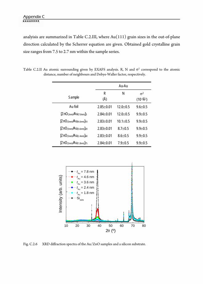
AAppppeennddiixx CC
analyisis are summarized in Table C.2.III, where Au(111) grain sizes in the out-of-plane
direction calculated by the Scherrer equation are given. Obtained gold crystalline grain
size ranges from 7.5 to 2.7 nm within the sample series.
Table C.2.II Au atomic surrounding given by EXAFS analysis. R, N and σ2 correspond to the atomic distance, number of neighbours and Debye-Waller factor, respectively.
Sample
Au-Au
R (Å)
N σ2 (10-3Å2)
Au foil 2.85±0.01 12.0±0.5 9.6±0.5
[ZnO(3nm)/Au(7.8nm)]5 2.84±0.01 12.0±0.5 9.9±0.5
[ZnO(3nm)/Au(4.6nm)]10 2.83±0.01 10.1±0.5 9.9±0.5
[ZnO(3nm)/Au(3.6nm)]20 2.83±0.01 8.7±0.5 9.9±0.5
[ZnO(3nm)/Au(2.4nm)]40 2.83±0.01 8.6±0.5 9.9±0.5
[ZnO(3nm)/Au(1.8nm)]75 2.84±0.01 7.9±0.5 9.9±0.5
10 20 30 40 50 60 70 80
Inte
nsity
(arb
. uni
ts)
2θ (º)
tAu = 7.8 nm tAu = 4.6 nm tAu = 3.6 nm tAu = 2.4 nm tAu = 1.8 nm Sisubs
Fig. C.2.6 XRD diffraction spectra of the Au/ZnO samples and a silicon substrate.

From Ferromagnetism to Noble Metal Nanoparticles Formation in the Si3N4 and ZnO Systems
217
Table. C.2.III XRD results summary: Au(111) peak position (2θ), full width at half maximum (FWHM) and its corresponding grain size in the out-of-plane direction obtained by the Scherrer equation. As well, effective Au-layer thickness (tAu) calculated from RBS data and Au NP diameter (φ) obtained by GISAXS.
Sample XRD-Au(111) RBS tAu (nm)
GISAXS φ (nm) 2θ (º) FWHM (º) grain size
[ZnO(3nm)/Au(7.8nm)]5 38.19 7.8 7.5 7.8 -
[ZnO(3nm)/Au(4.6nm)]10 38.14 4.6 4.6 4.6 -
[ZnO(3nm)/Au(3.6nm)]20 38.09 3.6 3.6 3.6 -
[ZnO(3nm)/Au(2.4nm)]40 38.06 2.4 2.8 2.4 4.7
[ZnO(3nm)/Au(1.8nm)]75 38.13 1.8 2.7 1.8 3.7
For tAu ≥ 3.6 nm, where formation of continuous Au-layers is expected, the
obtained XRD-Au grain sizes are nearly identical to the effective Au-layer thickness
calculated from RBS data considering Au bulk density (tAu). Therefore, the assumption
of the Au bulk density (ρAu = 5.9x10²² at/cm3) in these Au/ZnO samples becomes
justified.
For samples with tAu = 2.4 and 1.8 nm, larger nanocrystalline grain sizes in
comparison with the RBS effective Au-layer thickness (tAu) support the suggested non-
continuous Au growth in samples with tAu ≤ 2.4 nm. Gold crystalline grain sizes close to 3
nm compared to about 2 nm of effective thickness for these samples are found. On the
other hand, the Au crystalline sizes of these two samples (∼3 nm) are smaller than the
ones given by GISAXS, included in Table C.2.III ( ∼ 4 and 5 nm for tAu = 2.4 and 1.8 nm,
respectively). This fact can be easily understood considering than each Au NP may
consists of smaller nanocrystalline grains. Moreover, increase of the Au/ZnO interfacial
regions due to Au NP formation is usually related to an enhancement of the crystalline
disorder.
This situation slightly differs from the Au/Si3N4 case, where the Au diameters
obtained from XRD were of the same order as the ones obtained by GISAXS (Table
C.1.III). Another difference (not given in the table) is that, apart from Au(111),
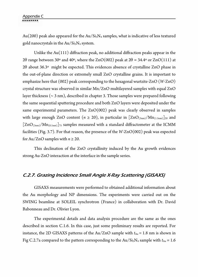
AAppppeennddiixx CC
Au(200) peak also appeared for the Au/Si3N4 samples, what is indicative of less textured
gold nanocrystals in the Au/Si3N4 system.
Unlike the Au(111) diffraction peak, no additional diffraction peaks appear in the
2θ range between 30º and 40º, where the ZnO(002) peak at 2θ = 34.4º or ZnO(111) at
2θ about 36.3º might be expected. This evidences absence of crystalline ZnO phase in
the out-of-plane direction or extremely small ZnO crystalline grains. It is important to
emphasize here that (002) peak corresponding to the hexagonal wurtzite-ZnO (W-ZnO)
crystal structure was observed in similar Mn/ZnO multilayered samples with equal ZnO
layer thickness (∼ 3 nm), described in chapter 3. Those samples were prepared following
the same sequential sputtering procedure and both ZnO layers were deposited under the
same experimental parameters. The ZnO(002) peak was clearly observed in samples
with large enough ZnO content (n ≥ 20), in particular in [ZnO(3nm)/Mn(1.5nm)]20 and
[ZnO(3nm)/Mn(0.1nm)]75 samples measured with a standard diffractometer at the ICMM
facilities (Fig. 3.7). For that reason, the presence of the W-ZnO(002) peak was expected
for Au/ZnO samples with n ≥ 20.
This declination of the ZnO crystallinity induced by the Au growth evidences
strong Au-ZnO interaction at the interface in the sample series.
C.2.7. Grazing Incidence Small Angle X-Ray Scattering (GISAXS)
GISAXS measurements were performed to obtained additional information about
the Au morphology and NP dimensions. The experiments were carried out on the
SWING beamline at SOLEIL synchrotron (France) in collaboration with Dr. David
Babonneau and Dr. Olivier Lyon.
The experimental details and data analysis procedure are the same as the ones
described in section C.1.6. In this case, just some preliminary results are reported. For
instance, the 2D GISAXS patterns of the Au/ZnO sample with tAu = 1.8 nm is shown in
Fig C.2.7a compared to the pattern corresponding to the Au/Si3N4 sample with tAu = 1.6

From Ferromagnetism to Noble Metal Nanoparticles Formation in the Si3N4 and ZnO Systems
219
nm (Fig C.2.7b), both with n = 75. The measured pattern presents features of Au NP
formation.
Bilayer thicknesses and NP sizes measured by this technique are given in Table C.2.IV.
For samples tAu = 1.8 nm and 1.6 nm, Bragg peaks indicate layering corresponding to
Λ about 4.9 nm and 4.8 nm respectively, well in agreement with the values determined by
XRR. A preliminary analysis gives average NP diameters of approximately φ = 4.7 nm
and φ = 3.7 nm for samples with tAu = 1.8 nm and tAu = 1.6 nm, respectively. Also
included in Table C.2.IV are the average Au cluster dimensions determined from XRD
measurements of the (111) Au reflection along the out-of-plane direction.
Fig. C.2.7 2D GISAXS patterns of [ZnO(3nm)/Au(1.8nm)]75 sample (left) and [Si3N4(6nm)/Au(1.6nm)]75 sample (right).
As it was indicated above, the Au crystalline grain sizes calculated by XRD are
slightly smaller than the φ values determined by GISAXS (see Table C.2.IV). This was
explained considering that not the all nanoparticle contributes to crystalline order,
existing Au amorphous fraction that leads to smaller XRD-φ values compared to GISAXS
ones. The Au amorphous contribution would be more important as the Au-layer
thickness is diminished, in the NP regime.

AAppppeennddiixx CC
The estimated Au NP density in these samples is about 4x10¹² NP/cm2 and 7x10¹²
NP/cm2 for tAu = 2.4 nm and tAu = 1.8 nm, respectively, which are considerably larger
than in the Au/Si3N4 system (∼2x10¹² NP/cm2), in agreement with the smaller NP size.
Higher NP density in the Au/ZnO system agrees with the shorter average in-plane
interparticle distances (L), also included in the table. For instance, L = 4.8 nm has been
estimated for the Au/ZnO sample with tAu = 1.8 nm, while nearly double separation (L =
8.3 nm) was found for the Au/Si3N4 sample with tAu = 1.6 nm. The NP density has been
calculated here in the same manner, by the total number of Au atoms measured by RBS
(at/cm2) divided by the number of atoms per NP obtained from the volume calculated
with the diameter φ, measured by GISAXS and the Au atomic density of 5.9x10²² at/cm3.
Table C.2.IV Structural characterization of samples with Au NP growth: XRR-obtained bilayer thickness
(XRR-Λ), GISAXS-obtained bilayer thickness (GISAXS-Λ), Au NP average diameter obtained by XRD (XRD-φ) and by GISAXS (GISAXS-φ). Au-layer NP density (NP/cm2) has been calculated using GISAXS-φ, the number of Au atoms per cm2 (RBS) and Au atomic density (ρAu = 5.9x10²² at/cm3). In-plane interparticle distance (L) has been obtained from Au NPs density and considering both square and hexagonal NP arranges. The given L value corresponds to the average.
Sample XRR-Λ
(nm) GISAXS-Λ
(nm) XRD-φ (nm)
GISAXS-φ (nm)
Au NPs (NP/cm2)
L (nm)
[ZnO(3nm)/Au(2.4nm)]40 5 4.9 2.8 4.7 4.4x10¹² 6.0
[ZnO(3nm)/Au(1.8nm)]75 5 4.8 2.7 3.7 6.8x10¹² 4.8
Regarding the structural parameters summarized in the table, it can be noticed,
similarly to what we observed for Au NPs in Si3N4, that Au NPs are also separated in
plane by a value close to 3/2 of φ distance for both Au/ZnO samples. For each sample,
the obtained average in-plane interparticle distance (L) and out-of-plane periodicity (Λ)
have again similar values (about 5 nm in this case).

From Ferromagnetism to Noble Metal Nanoparticles Formation in the Si3N4 and ZnO Systems
221
C.2.8. UV-VIS Absorption
Au NPs samples on quartz substrates were used to measure sample optical
absorption in transmission mode. The optical absorption of these films was measured
with a Cary 4000 UV-vis spectrophotometer at the ICMM, in the 200–900 nm
ultraviolet-visible range.
Fig. C.2.8(a) shows the optical density spectra as a function of wavelength of
samples with tAu ranging from 7.8 to 2.4 nm. The absorption coefficient spectra are also
given in Fig. C.2.8(b) for further comparison. The spectrum of sample with tAu = 1.8 nm
(75 bilayers) has not been included since its optical density results too high to be
accurately measured. Optical absorption from a ZnO film has been included for
comparison. For these samples, differing from the Au/Si3N4 system, no surface plasmon
resonance (SPR) is observed. For the particular case of tAu = 2.4 nm sample, for what Au
NP formation (φ ∼ 4 nm) was pointed by GISAXS, absorption at higher wavelengths
slightly differs from the other samples, where continuous Au/ZnO layers are expected.
Nonetheless, SPR is not observed in the Au/ZnO samples. The absence of SPR in these
as-grown samples agrees with the results recently reported by Sangpour et al.6 about gold
NPs formation in co-sputtered Au-SiO2 thin films, where no absorption peak was
observed for the as-deposited films. A broad SPR absorption band appeared after
annealing at 800ºC, leading to Au NP of about 30 nm size uniformly distributed on the
surface.
Taking into consideration all the obtained results, it appears that for Au/ZnO
samples with tAu = 1.8 nm and 2.4 nm, the Au NPs pointed out by GISAXS might be in
fact not as well formed as expected.
The situation could be related to the one recently observed by Lee et al. for Au and
Ag-ZnO composite nanocrystals prepared by solution-phase synthesis.7 They found that
the noble metal-ZnO systems do not form a core-shell structure despite the small lattice
parameter difference between Au (or Ag) and ZnO. Conversely, a dumbbell-like
structure was evidenced by HRTEM studies, being the average sizes in this case ∼ 4 and
∼ 10 nm for the noble metals and the ZnO.

AAppppeennddiixx CC
200 300 400 500 600 700 800 9000
1
2
3
4
200 300 400 500 600 700 800 900
Opt
ical
Den
sity
Wavelength (nm)
tAu
= 2.4 nm
tAu = 3.6 nm
ZnO film
tAu = 7.8 nm
tAu = 4.6 nm
(a)
Abs
orpt
ion
Coe
ffici
ent (
cm-1)
Wavelength (nm)
ZnO film
tAu
= 2.4 nm
tAu = 3.6 nm
tAu
= 7.8 nmtAu
= 4.6 nm
(b)
Fig. C.2.8 Optical density (a) and absorption coefficient (b) spectra of Au/ZnO samples with tAu = 7.8
nm, 4.6 nm, 3.6 nm and 2.4 nm (φ = 5.1 nm). A sputtered ZnO film has been included for comparison.
Fig. C.2.9 Mechanism for the formation of Au- and Ag-ZnO nanocrystals by solution-phase synthesis suggested by Lee et al.7
The suggested mechanism for the formation of Au- and Ag-ZnO nanocrystals by
this aqueous solution method is shown in Fig. C.2.9. They assigned the formation of

From Ferromagnetism to Noble Metal Nanoparticles Formation in the Si3N4 and ZnO Systems
223
dumbbell-like structures to differences in the crystalline structure between them. Due to
the crystal structure mismatch (∼17%), the interfacial energy would be too large, and
thus to reduce the total free energy of the system, the dumbbell-like structure could form
instead of core-shell structure.
It should be noted that we cannot make direct comparisons since Au/ZnO
preparation by sequential sputtering significantly differs from Au/ZnO growth by
solution-phase synthesis. Nonetheless, the reported Au/ZnO tendency to dumbbell-like
structures over core-shell ones might be associated with Au-ZnO interface tensions or
defected interfacial regions in our samples that may lead to not very well formed Au NPs
poorly distributed inside ZnO and nonappearance of SPR phenomenon. The existence
of a significant Au-ZnO interaction at the interface has been evidenced by XRD
experiments, which has shown i) declination of the ZnO crystallinity induced by the Au
growth and ii) Au(111) texture favoured by the ZnO presence. Furthermore, XRR
experiments have shown that out-of-plane periodicity gets declined for the Au/ZnO
system compared to the Au/Si3N4 one for tAu = 1.8 nm and 2.4 nm, evoking less well
formed or worse organized Au NPs inside ZnO. Moreover, analysis of XRR-Λ values
along the sample series has pointed out that formation of Au NPs is further favoured
using Si3N4 than ZnO as matrix material by this preparation method since the transition
from Au continuous layer to Au NP growth is much more abrupt as well as beginning
from longer Au sputtering times in the case of Au/Si3N4 samples.
C.2.9. Conclusions
With the aim of growing Au NPs inside a different matrix with similar refractive
index as Si3N4 in a controlled way, a series of Au/ZnO samples has been prepared by
sequential sputtering technique, keeping constant the ZnO layer thickness and
modifying the effective Au layer thickness (tAu).
A change in the Au-layer morphology with the deposited Au amount has been
evidenced by XRR and GISAXS results. Continuous Au layers leading to multilayered
samples have been found for tAu ≥ 3.6 nm, being the Au-layer continuous growth

AAppppeennddiixx CC
preserved until shorter Au-layer sputtering times than in the case of Au/ samples. Non-
continuous Au-layers resulting in Au NPs inside the ZnO matrix have been evidenced for
tAu = 2.4 nm and 1.8 nm.
Smaller Au NPs have been obtained in ZnO than in the Si3N4 matrix. Average NP
sizes between 5 – 4 nm have been found in ZnO compared to 7 – 5 nm in Si3N4. The Au
NP density varies within the Au/ZnO series, ranging between 4x10¹² NP/cm2 and 7x10¹²
NP/cm2, which are considerably larger than for the Si3N4 matrix (∼2x10¹² NP/cm2),
according to smaller NP size and shorter average in-plane interparticle distances (L = 5 –
6 nm for ZnO versus L = 8 – 10 nm for Si3N4 matrix).
For the Au/ZnO samples, UV-vis absorption spectrum has not shown surface
plasmon resonance (SPR) effect.
The absence of SPR phenomenon in these samples has been related to possible
Au-ZnO interface tensions or defected interfacial regions in our samples that may lead to
not very well formed Au NPs poorly distributed inside ZnO. Significant interaction at the
Au-ZnO interface has been confirmed by XRD.
References 1 S. Link and M. A. El-Sayed, J. Phys. Chem. B 103, 8410 (1999).
2 L. Arlemao, D. Barreca, G. Bottaro, A. Gasparotto, S. Gross, C. Maragno, E. Tondello, Coordination Chemistry Reviews 250, 1294 (2006).
3 E. Kotai, Nucl. Instrum. Methods B 85, 588 (1994).
4 SAMBA at www.synchrotron-soleil.fr
5 Outils et méthodes pour l’analyse des spectres EXAFS/www.icmpe.cnrs.fr/spip.php rubrique 340
6 P. Sangpour, O. Akhavan, A. Z. Moshfegh, M. Roozbehi, Appl. Surf. Sci. 254, 286 (2007).
7 M. Lee, T. G. Kim, W. Kim and Y. Sung, J. Phys. Chem. C 112, 10079 (2008).
225
GENERAL CONCLUSIONS
Different series of Mn-Zn-O films have been prepared ([Mn(t)/ZnO(3nm)]n
multilayers, [MnOx(t)/ZnO(3nm)]n multilayers and Zn0.95Mn0.05O thin films) in order
to gather further knowledge of the nature of the ferromagnetic ordering in this
system. For all the samples series, room temperature ferromagnetism (RTFM), as
well as an evolution of the magnetic response within each series, has been observed.
The sensitivity of the magnetic properties to the Mn oxidation state in each sample has been found to be a common characteristic in this study.
For [Mn(t)/ZnO(3nm)]n multilayers, XANES studies have revealed an absence of
metallic Mn and that the average Mn oxidation state increases from +2.1 to +3.3 as
the thickness of the Mn layer (t) diminishes. A weak ferromagnetic signal above
room temperature has been found in multilayers with larger values of t while mostly
paramagnetic-like signals have been found in samples with very thin Mn layers (t ≤
0.7 nm), where formation of amorphous MnO2 clusters inside the ZnO matrix has
been evidenced. For the obtained ferromagnetic samples (t ≥ 3 nm), EXAFS,
XANES, HRTEM and XRD have indicated the coexistence of Mn2+ in rocksalt (RS)
and wurtzite (W) phases. Results suggest non-homogeneously intermixed layers,
with Mn and Zn highly diffused into both ZnO and Mn oxide rich-regions, leading to
both Zn-O-Mn (W-type) and Mn-O-Zn (RS-type) mixed phases. Saturation
magnetization values scale with the Mn content in Zn-O-Mn (W-phase), what points at Mn2+ in ZnO wurtzite phase as the responsible of the weak ferromagnetic signal.
For [MnOx(t)/ZnO(3nm)]75 multilayers, MnO2-δ nano-sized grains embedded in W-
ZnO (with Mn/Zn ratio about 4 at.%) have been obtained by oxidizing both Zn and
Mn during growth. Stronger RTFM, with MS values reaching 0.8 μB per Mn atom,
has been found here, where results suggest ferromagnetism due to Mn3+ and Mn4+
interacting via double-exchange mechanism under the effect of the neighbouring
ZnO. The coexistence of Mn3+ and Mn4+ has been unambiguously confirmed by Mn K-edge and Mn L3,2-edge measurements.

These different approaches to the study of the role of interfaces and the Mn
oxidation state in the Mn-Zn-O system have indicated two possible kinds of
ferromagnetic interaction in this system, which are greatly influenced by the
particular Mn oxidization or reduction process during growth. Reduction of an
initially highly oxidized Mn phase by the surrounding ZnO effect has led to
ferromagnetic order via double exchange. By contrast, just a small paramagnetic-like
signal has been found in originally metallic Mn that highly oxidized during growth.
For this former series, a FM signal has only been obtained when the average Mn
oxidation state is close to +2, case where FM based on the magnetic interactions between the Mn2+ cations in a wurtzite Zn-O-Mn phase is suggested.
RTFM due to Mn2+ in ZnO lattice forming Zn-O-Mn wurtzite phase has been also
observed in Mn:ZnO films prepared by sputtering from a Zn0.95Mn0.05O target,
where a strong variation of the ferromagnetic response has been obtained by
modifying the working gas type (Ar, Ar/N2, Ar/O2). The highest MS values have
been obtained for the Ar− and Ar/N2−prepared Mn:ZnO films and results are in
agreement with RTFM ordering in n-type Mn:ZnO mediated by electron carriers.
Both preparation using Ar/O2 and post-deposition annealings in oxygen lead to highly oxidized Mn, close to Mn4+ and a significant reduction of the ferromagnetism.
It has been found that improvement of the crystal quality of samples, high oxidation
of Mn during growth or after deposition as well as promoting rocksalt phase over the
wurtzite one are common features leading to the weakening of the ferromagnetism in
this system, whose origin is mostly associated with Mn2+ in W-ZnO. High oxidization
of Mn during the early growth process only favours ferromagnetism under certain
conditions, where surrounding ZnO seem to favour MnO2 reduction and the
interaction between Mn3+ and Mn4+ by double-exchange. These specific conditions
leading to RTFM by double-exchange mechanism have been found to be more
difficult to stabilize than formation of the Zn-O-Mn W-phase. The coexistence of
Mn3+ and Mn4+ is necessary but not sufficient for the FM ordering of the system.

227
Moreover, the magnetic, structural and electronic properties of Mn/Si3N4
multilayers have been studied in this work for the first time, reporting RTFM in this
system. The origin of ferromagnetism here has been ascribed from the formation of a
distorted non-centrosymmetric Mn3N2 phase with slightly shorter Mn-N distances.
Changes in the unit cell volume have been commonly considered theoretically in
order to promote transitions from the AFM ground state to a FM phase in
manganese nitrides. XMCD has shown that the magnetism in the films is due to the
Mn d5 (Mn2+) state and XANES calculations have confirmed the presence of a
Mn3N2 phase with non-centrosymmetric Mn symmetry, which seems to be favored
by the tetrahedral Si-N4 arrange in the Si3N4 structure. An evolution of the magnetic
properties within the sample series has been found depending on the Mn and Si3N4 layer thickness, explaining this variation in terms of the Mn3N2 phase.
In addition, the growth of Au nanoparticles embedded in both ZnO and Si3N4
systems has been also studied by preparing Au/ZnO and Au/Si3N4 series by
sequential sputtering. A change in the Au-layer morphology with the deposited Au
amount has been evidenced by XRR and GISAXS in the two systems, obtaining Au
NPs for tAu ≤ 2.4 mm in the ZnO matrix and for tAu ≤ 2.9 mm in the Si3N4 one.
Average NP sizes between 5 - 4 nm have been found in ZnO compared to 7 - 5 nm in
Si3N4. Au NP density ranges between 4x10¹² NP/cm2 and 7x10¹² NP/cm2 in the
ZnO series, being considerably larger than in the Si3N4 matrix (∼2x10¹² NP/cm2),
according to a smaller NP size and a shorter average in-plane interparticle distance for ZnO.
For the Au/ZnO samples, surface plasmon resonance (SPR) effect has not been
observed, fact that has been related to possible Au-ZnO interface tensions or
defected interfacial regions in these samples that may have lead to poorly formed Au NPs insufficiently distributed inside ZnO.
For the Au/Si3N4 samples, different Au NP distributions have been found by
GISAXS, evidencing Au NPs (φ = 7 nm) with in-plane spatial correlation for tAu = 2.9

nm sample while Au NPs (φ = 5 nm) without spatial correlation for tAu = 1.6 nm. For
both samples, UV-vis absorption has shown a surface plasmon resonance (SPR),
which shifts towards longer wavelengths with increasing the Au-layer effective
thickness, in agreement with the theory. A variation of the SPR maximum with the
effective Au-layer thickness has been obtained, which makes the Au/Si3N4 system
tunable for optical applications requiring a specific absorption spectrum.

Conclusiones Generales
229
CONCLUSIONES GENERALES
Se han preparado distintas series de muestras del sistema Mn-Zn-O en forma de
lámina delgada (multicapas [Mn(t)/ZnO(3nm)]n, multicapas [MnOx(t)/ZnO(3nm)]n y
láminas delgadas de tipo Zn0.95Mn0.05O) con el objetivo de lograr una mayor
comprensión de la naturaleza del ordenamiento ferromagnético en este sistema. En
todas las series de muestras estudiadas se ha observado ferromagnetismo a
temperatura ambiente (RTFM) así como una evolución de la respuesta magnética
en cada serie. Una característica común en todas las muestras estudiadas es la fuerte dependencia de las propiedades magnéticas con el estado de oxidación de Mn.
En el caso de las multicapas denominadas [Mn(t)/ZnO(3nm)]n, estudios de XANES
han demostrado ausencia de Mn metálico en las muestras, así como un aumento del
estado de oxidación promedio de Mn, de +2.1 a +3.3, a medida que disminuye el
grosor de la capa de Mn (t) dentro de la serie. Las multicapas con los valores de t mayores presentan una pequeña señal ferromagnética a temperatura ambiente,
mientras que únicamente una contribución de tipo paramagnético se ha observado
en las muestras con capas de Mn muy delgadas (t ≤ 0.7 nm), constituidas
principalmente por agregados amorfos de MnO2 en la matriz de ZnO. En las
muestras ferromagnéticas, los estudios realizados mediante EXAFS, XANES,
HRTEM y XRD muestran la coexistencia de Mn2+ en dos fases distintas, tipo cloruro
sódico (RS) y wurtzita (W). Los resultados obtenidos sugieren la existencia de capas
ricas en óxido de Mn (tipo RS) y ricas en ZnO (tipo W), en las que los fenómenos de
interdifusión de Zn y Mn dan lugar a la formación de dos de dos fases mixtas no
homogéneas denominadas Zn-O-Mn (W) y Mn-O-Zn (RS), que coexisten en estas
muestras. Se ha encontrado que la imanación de saturación escala con la cantidad de
Mn en la fase W (Zn-O-Mn), lo que apunta a que sólo el Mn2+ en ZnO con fase wurtzita es responsable de la pequeña señal ferromagnética observada.
En el caso de las multicapas denominadas [MnOx(t)/ZnO(3nm)]75, los estudios
realizados muestran la formación de pequeños agregados de MnO2-δ dentro de W-
ZnO (en una relación Mn/Zn de aproximadamente 4 % at.) obtenidos mediante
oxidación de Zn y de Mn durante el proceso de preparación. Se ha encontrado
ferromagnetismo a temperatura ambiente, con valores de imanación de saturación
(MS) considerablemente mayores que en el caso anterior, alcanzando 0.8 μB por
átomo de Mn. Los resultados apuntan a que el origen del ferromagnetismo en estas
muestras reside en la interacción de doble-canje entre Mn3+ and Mn4+, promovida
por el efecto reductor del ZnO situado en las proximidades. La coexistencia de Mn3+ y Mn4+ ha sido corroborada mediante experimentos de XAS los bordes K y L del Mn.
Las dos vías utilizadas para el estudio de los fenómenos de intercara y del estado de
oxidación de Mn en el magnetismo del sistema Mn-Zn-O han puesto de manifiesto
la posibilidad de dos tipos de interacciones ferromagnéticas distintas en este sistema,
las cuales son muy dependientes del proceso particular de oxidación o reducción del
Mn durante el crecimiento. Por un lado, la reducción de una fase de Mn altamente
oxidada durante el depósito por el efecto del ZnO próximo se ha asociado con
ferromagnetismo por doble-canje. A diferencia, Mn originariamente metálico que
sufre una elevada oxidación durante el crecimiento únicamente presenta un
comportamiento tipo paramagnético. Partiendo de Mn metálico, se ha encontrado
orden ferromagnético únicamente en muestras con estados de oxidación promedio
de Mn cercanos a +2, donde el ordenamiento ferromagnético se ha asociado con la interacción entre los cationes Mn2+ de una fase Zn-O-Mn tipo wurtzita.
Se ha conseguido también ferromagnetismo a temperatura ambiente (RTFM) en
muestras con Mn2+ en la red de ZnO formando una fase Zn-O-Mn tipo wurtzita en
láminas de Mn:ZnO preparadas por pulverización catódica de un blanco de
composición Zn0.95Mn0.05O, en las que se ha observado una fuerte variación de la
respuesta magnética en función del tipo de gas durante el depósito (Ar, Ar/N2,
Ar/O2). Los valores de MS más altos corresponden a las láminas de Mn:ZnO
preparadas con Ar y con Ar/N2, en este orden, y los resultados obtenidos avalan la
existencia de ferromagnetismo mediado por los electrones en muestras tipo n con

Conclusiones Generales
231
Mn2+ diluido en ZnO. Tanto la preparación de láminas en atmósfera de Ar/O2 como
el recocido posterior de las muestras en atmósfera de oxígeno dan lugar a estado de
oxidación promedio de Mn elevado, próximo a Mn4+ y una considerable reducción del ferromagnetismo.
Factores como la mejora de la calidad cristalina de las muestras, la alta oxidación del
Mn durante el crecimiento o tras la preparación, así como el aumento de fase tipo
NaCl frente a wurtzita constituyen características comunes relacionadas con el
deterioro del ferromagnetismo en este sistema, asociado principalmente a Mn2+ en W-ZnO.
La alta oxidación inicial del Mn en el proceso de crecimiento únicamente favorece el
ferromagnetismo en ciertas condiciones particulares, bajo las cuales el ZnO cercano
al MnO2 favorece la reducción del MnO2 y la interacción entre Mn3+ y Mn4+ vía
doble-canje. Sin embargo, los resultados obtenidos indican que las condiciones
necesarias para lograr ordenamiento ferromagnético a través de doble-canje en este
sistema son considerablemente más difíciles de estabilizar que la formación de Zn-O-
Mn con fase wurtzita. La coexistencia de Mn3+ y Mn4+ no es suficiente para el ordenamiento ferromagnético del sistema.
Por otro lado, las propiedades magnéticas, estructurales y electrónicas de multicapas
de Mn/Si3N4 han sido estudiadas por vez primera, con la obtención de
ferromagnetismo por encima de temperatura ambiente. El origen del
ferromagnetismo se ha explicado mediante la formación de una fase no centro-
simétrica y distorsionada de Mn3N2, con distancias Mn-N ligeramente inferiores a las
existentes en Mn3N2, lo que está de acuerdo con las modificaciones del volumen de
la celda unidad consideradas frecuentemente en estudios teóricos sobre transiciones
entre estados fundamentales antiferromagnéticos y ferromagnéticos en nitruros de
manganeso. XMCD ha demostrado que el magnetismo de estas muestras procede de
Mn d5 (Mn2+) y cálculos de XANES han confirmado la presencia de la fase Mn3N2
con entorno de Mn no centrosimétrico, posiblemente favorecido por el

ordenamiento tetraédrico de tipo Si-N4 del Si3N4. Se ha observado una evolución de
las propiedades magnéticas de las muestras al modificar los grosores de las capas de Mn y de Si3N4, explicando esta variación en función de la fase de Mn3N2 formada.
Además, se han llevado a cabo estudios del crecimiento de nanopartículas (NPs) de
Au en ambas matrices, ZnO y Si3N4, preparadas mediante sputtering secuencial.
Estudios de XRR y GISAXS han mostrado un cambio en la morfología de la capa de
Au en función de la cantidad de Au depositada, indicando formación de NPs de Au
para tAu ≤ 2.4 nm, en el caso de ZnO, y para tAu ≤ 2.9 nm, en el caso de Si3N4. El
tamaño promedio de las NPs de Au obtenidas es de 5-4 nm en la serie de ZnO y de
7-5 nm en la de Si3N4. La densidad de NPs de Au varía entre 4x10¹² NP/cm2 y 7x10¹²
NP/cm2 en la serie de ZnO, siendo considerablemente más grande que en la serie de
Si3N4 (∼2x10¹² NP/cm2), de acuerdo con el menor tamaño y la menor separación entre NPs en la matriz de ZnO.
En el caso de las muestras Au/Si3N4, GISAXS ha evidenciado distintos tipos de
distribución de las NPs, obteniéndose NPs de Au (φ = 7 nm) con correlación
espacial en el plano para tAu = 2.9 nm y NPs de Au (φ = 5 nm) sin correlación espacial para tAu = 1.6 nm.
Ambas distribuciones de Au/Si3N4 presentan resonancia de plasmón de superficie
(SPR), desplazándose el máximo hacia longitudes de onda mayores al aumentar el
grosor de la capa efectiva de Au, como predice la teoría. La variación obtenida en la
posición del plasmón de superficie en función del grosor de Au efectivo pone de manifiesto el interés del sistema Au/Si3N4 en aplicaciones ópticas.
En el caso de las muestras Au/ZnO, no se ha observado resonancia de plasmón de
superficie (SPR), hecho que se ha relacionado con la existencia de tensiones o zonas
defectuosas en las intercaras Au-ZnO, pudiendo dar lugar a NPs de Au peor formadas o distribuidas de manera inhomogénea dentro de la matriz.

233
Agradecimientos
Son muchas las personas que han contribuido de una u otra manera a la realización
de este trabajo. A todas ellas quiero expresar mi más sincero agradecimiento.
En primer lugar a mi director de tesis, Carlos Prieto, por toda la dedicación, ilusión
y esfuerzo puestos en este trabajo y por toda la ayuda, paciencia y confianza en mí a lo
largo de estos años. Gracias, Carlos, siempre serás un referente para mí.
A Luisa Bausá, mi tutora, por su ayuda y disponibilidad.
Al grupo de investigación, Alicia de Andrés, Federico Mompeán, Rafa Jiménez y
Mar García, por el apoyo recibido.
A todas las colaboraciones. Gracias a Agnès Traverse por la estancia en París, por
tanta amabilidad y comprensión y por las aportaciones tanto científicas como personales.
Gracias también a Johann y al grupo de CLIO. A Augusto Barrós y al Instituto de
Engenharia Cerâmica e do Vidro por la estancia en Aveiro, por las medidas de TEM y por
toda la ayuda ofrecida. A Javier García por las medidas y los análisis de RBS y NRA. A
Jesús Chaboy por los cálculos de XANES. A Yves Huttel y a Elisa Román por las medidas
de XPS. A Luisa Ruiz González y a José María González Calbet por las medidas de
HRTEM. A Neil Telling y a Gerrit Van der Laan por los experimentos de XAS y de
XMCD en el borde L. A Olivier Lyon y David Babonneau por las medidas y el análisis de
GISAXS. A Ángel de Pablos por ayudarme con los blancos de sputtering. A Emiliano
Fonda por su asistencia en SAMBA y a toda la gente de SpLine por su asistencia y apoyo
en tantas ocasiones. Gracias, Germán Castro, por tu ayuda. Ha sido un placer colaborar
con todos vosotros.
Al mejor becario mayor que se puede imaginar, Félix, incapaz de reflejar tanta
gratitud, y a Merche, por su tan eficiente ayuda y por transmitir tanto entusiasmo.
A Ana, mi compañera de tesis y de tantos años, gracias por estar siempre ahí. A
Isabel, María, Marisa, Jorge, Rocío, Edu, Ainhara, Raúl y Ainhoa, por hacer los días en el
Instituto tan agradables. A Argelia, por la buena onda que nos diste. A Riccardo y los

AAggrraaddeecciimmiieennttooss
“fotónicos”, por los buenos ratos en el 004 y alrededores. A Jorge, Norbert y Luis Balo,
por la ayuda con medidas y cacharreos de laboratorio varios. Al “Club Valdelatillas”, al
mejor personal trainer, Javi y al resto de más o menos sufridores, Mariano, Elvira, Lidia,
Quique…gracias equipo por tantos buenos momentos, agujetas incluidas. Gracias
también al Grupo de Teatro por tantas risas.
Gracias a todo el personal científico, técnico y administrativo del Instituto de
Ciencia de Materiales y al CSIC, por la oportunidad de disfrutar una beca.
A mis compañeros de la Facultad (gracias Alberto por cuidarme tanto) incluidos
los que ya no están (gracias Claudio, imposible olvidarte).
A mis compis de piso, las de siempre y los de ahora, mi pequeña familia de
Meléndez, gracias por vuestra comprensión y por ese “buen rollito”.
A mis amigas de la resi y a las de Albacete de toda la vida, por vuestro interés en mi trabajo durante todos estos años.
Al apoyo incondicional de toda mi familia. A mi hermana Ana, por tanta motivación, a la peque, a Toni y a mis hermanos Juanjo y Ernesto. Gracias Pepe, por tus consejos, y gracias Mamá, por darme muchísimo más que la vida.
Y gracias a ti, Emilio, por tu ayuda, por escucharme y por hacerme tan feliz cada día.
