fermilab initiatives in 3d integrated circuits and soi...
TRANSCRIPT

May 2006 ILC VTX Workshop at Ringberg 1
Fermilab Initiatives in 3D Integrated Circuits and SOI
Design for HEP
Ray YaremaFor ILC Pixel Group at Fermilab
ILC Vertex WorkshopRingberg Castle, Tegernsee. Germany
May 29-31, 2006

May 2006 ILC VTX Workshop at Ringberg 2
Introduction• 3D integrated circuits is becoming a topic of interest
in many technical journals and conferences. 1,2 (Note: As you will see, this is different than 3D detectors often described in the HEP literature.)
• This work can provide new opportunities for us to explore issues such as:– Low mass– High density– Increased functionality
• This talk will present– An overview of 3D IC principles– Three examples of 3D ICs– A design showing a 3D circuit for HEP– SOI Sensor development projects

May 2006 ILC VTX Workshop at Ringberg 3
What is a 3D Integrated Circuit?• A 3D chip is
comprised or 2 or more layers of semiconductor devices which have been thinned, bonded together, and interconnected to form a “monolithic”circuit.
• Frequently, the layers (also called tiers) are comprised of devices made in different technologies.
Opto Electronics
Digital layer
Analog Layer
Sensor Layer
Optical Fiber In Optical Fiber Out
Designer’s Dream
50 um

May 2006 ILC VTX Workshop at Ringberg 4
Why Consider 3D Now?• The move to 3D is being driven entirely by
industry needs.– In submicron processes, RC delay is a limiting
factor in performance improvement.– Low k dielectrics to reduce C have been difficult
to implement.– Circuit overhead is taking a larger fraction of the
chip area.• 3D is discussed in the ITRS (International
Technology Roadmap for Semiconductors) as an approach to improve circuit performance and permit continuation of Moore’s Law.

May 2006 ILC VTX Workshop at Ringberg 5
What are the Advantages?• Going 3D reduces trace length
– Reduces R, L, C– Improves speed– Reduces interconnect power, crosstalk
• Reduces chip size• Processing for each layer can be optimized• MAPS as an example
– 100% diode fill factor– Four-side abuttable devices
Conventional MAPS Layout93D Pixel Layout9
3D Routing (small chip)2D Routing (large chip)

May 2006 ILC VTX Workshop at Ringberg 6
Who is Working on 3D ICs?
USA:Albany NanocenterU. Of Kansas, U of ArkansasLincoln Labs, AT&TMIT,RPI, RTI, TIIBM, Intel, Irvine SensorsMicron, Sandia LabsTessera, Tezzaron,Vertical Circuits, Ziptronix
Europe: Fraunhofer IZM, IMEC Delft,Infineon, Phillips, Thales, Alcatel Espace,NMRC, CEA-LETI, EPFL, TU Berlin
Asia:ASET, NEC, University of Tokyo,Tohoku University, CREST,Fujitsu, ZyCube, Sanyo,Toshiba, Denso, Mitsubishi, Sharp,Hitachi, Matsushita, Samsung

May 2006 ILC VTX Workshop at Ringberg 7
Groups are Pursuing Different Options
• The different organizations are taking many different approaches to 3D fabrication.3
• The approaches can be divided into 2 general categories:– Wafer to wafer
bonding– Die to wafer bonding
Wafer to wafer bonding
Die to wafer bonding

May 2006 ILC VTX Workshop at Ringberg 8
Advantages and Disadvantages• Wafer to wafer bonding approach
– Advantages• All work generally handled by one fabricator• Thinner tiers with shorter vias are possible
– Disadvantages • Dies must be same size• Precise alignment across wafer is essential.• Yield is reduced with the number of layers.
• Die to wafer bonding approach– Advantages
• Different vendors can be used for different tiers• Known good die can be used to improve yield
– Disadvantages• More handling of individual parts
May 2006 ILC VTX Workshop at Ringberg 9
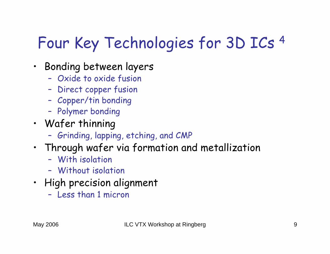
Four Key Technologies for 3D ICs 4
• Bonding between layers– Oxide to oxide fusion– Direct copper fusion– Copper/tin bonding– Polymer bonding
• Wafer thinning– Grinding, lapping, etching, and CMP
• Through wafer via formation and metallization– With isolation– Without isolation
• High precision alignment– Less than 1 micron
May 2006 ILC VTX Workshop at Ringberg 10
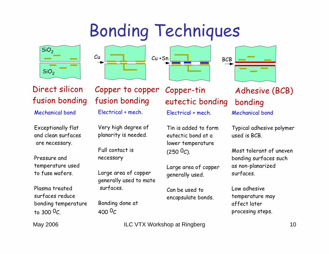
Bonding Techniques
Direct siliconfusion bonding
Copper to copperfusion bonding
Copper-tineutectic bonding
Adhesive (BCB)bonding
SiO2
SiO2Cu Cu +Sn BCB
Mechanical bond
Exceptionally flatand clean surfacesare necessary.
Pressure andtemperature usedto fuse wafers.
Plasma treatedsurfaces reducebonding temperatureto 300 0C.
Mechanical bond
Typical adhesive polymerused is BCB.
Most tolerant of unevenbonding surfaces suchas non-planarizedsurfaces.
Low adhesivetemperature mayaffect laterprocesing steps.
Electrical + mech.
Very high degree ofplanarity is needed.
Full contact isnecessary
Large area of coppergenerally used to matesurfaces.
Bonding done at400 0C
Electrical + mech.
Tin is added to formeutectic bond at alower temperature(250 0C).
Large area of coppergenerally used.
Can be used toencapsulate bonds.
May 2006 ILC VTX Workshop at Ringberg 11
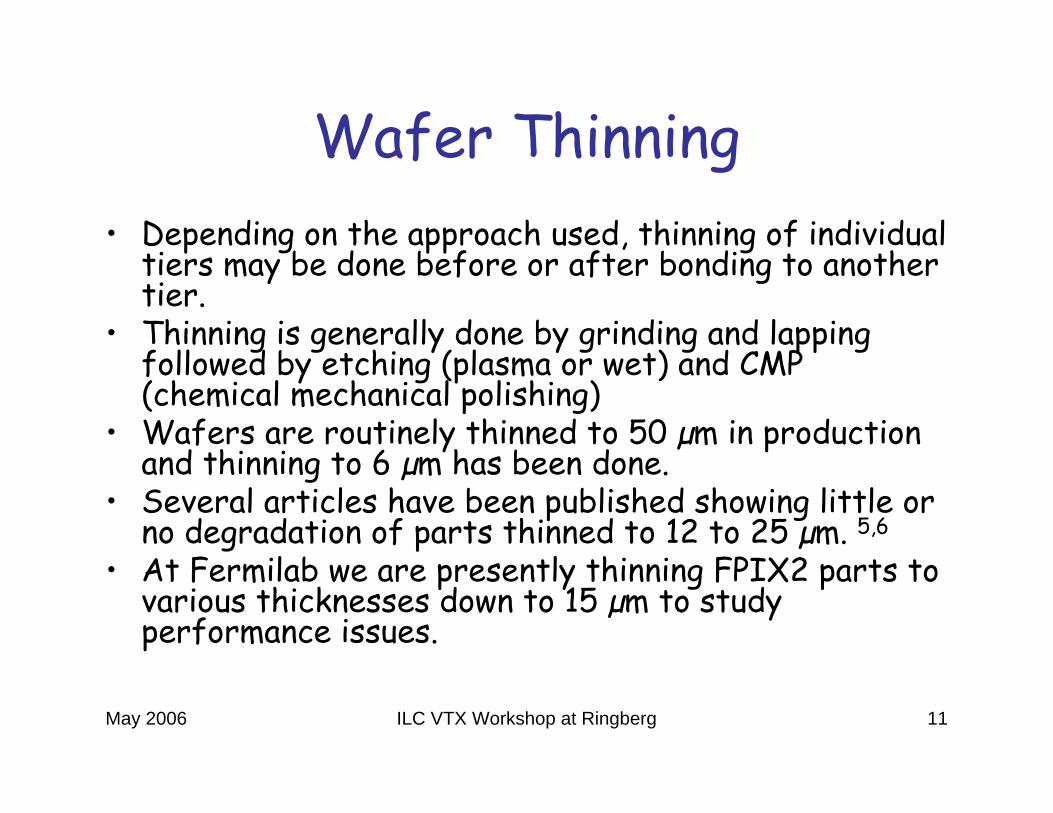
Wafer Thinning• Depending on the approach used, thinning of individual
tiers may be done before or after bonding to another tier.
• Thinning is generally done by grinding and lapping followed by etching (plasma or wet) and CMP (chemical mechanical polishing)
• Wafers are routinely thinned to 50 µm in production and thinning to 6 µm has been done.
• Several articles have been published showing little or no degradation of parts thinned to 12 to 25 µm. 5,6
• At Fermilab we are presently thinning FPIX2 parts to various thicknesses down to 15 µm to study performance issues.
May 2006 ILC VTX Workshop at Ringberg 12
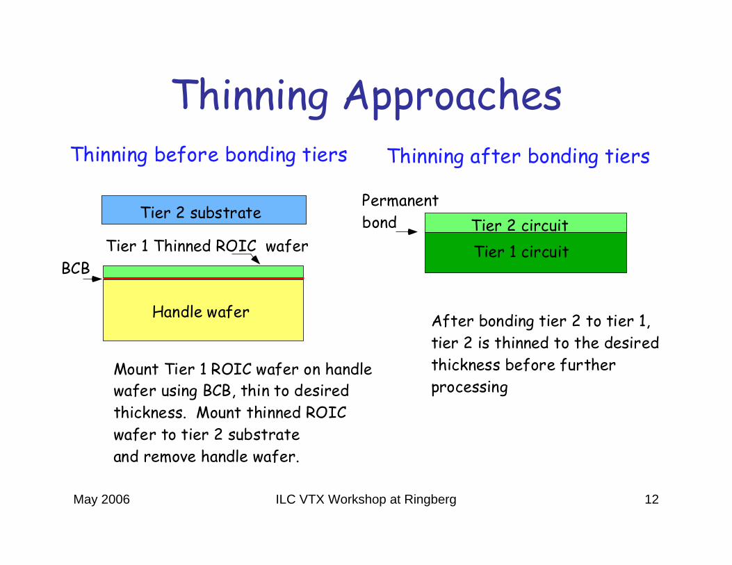
Thinning Approaches
Handle wafer
BCBTier 1 Thinned ROIC wafer
Mount Tier 1 ROIC wafer on handlewafer using BCB, thin to desiredthickness. Mount thinned ROICwafer to tier 2 substrateand remove handle wafer.
Thinning before bonding tiers
Permanentbond
Tier 1 circuitTier 2 circuit
After bonding tier 2 to tier 1,tier 2 is thinned to the desiredthickness before furtherprocessing
Thinning after bonding tiers
Tier 2 substrate
May 2006 ILC VTX Workshop at Ringberg 13
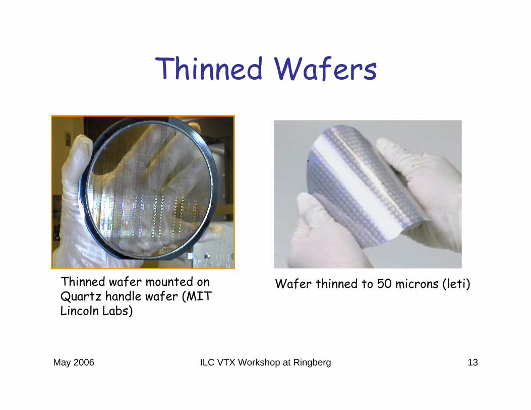
Thinned Wafers
Thinned wafer mounted onQuartz handle wafer (MITLincoln Labs)
Wafer thinned to 50 microns (leti)

May 2006 ILC VTX Workshop at Ringberg 14
Wafer Via Formation• Two different techniques are used for via formation
depending on the type of the substrate.– For vias in silicon (CMOS), the Bosch process (SF6) is used to
etch very deep vias (up to 400 um) with nearly vertical side walls. 7
– For vias in oxide (SOI), a standard plasma etching process is used, resulting in tapered side walls
• Isolation– In CMOS wafers, the via walls must be insulated (C4F8)
before filling with metal– In SOI wafers, no passivation is necessary (advantage for
SOI)• Vias are filled TiN/Cu or tungsten• Vias as small as 1.5 um have been made

May 2006 ILC VTX Workshop at Ringberg 15
Via Formation
SEM of 3 vias made with Bosch process 7
Close-up of walls with/withoutScallops in Bosch process 7
Tapered wall using high density plasma oxide etch(MIT Lincoln Labs)

May 2006 ILC VTX Workshop at Ringberg 16
Alignment• Need wafer-to-
wafer alignment accuracy compatible with a submicron 3D Via
• Tools used based on modern IC wafer stepper technology
• 0.5 µm 3-sigma overlay demonstrated at MIT LL.
6-axis PZT stage
Laser interferometer controlled XY stage
Bottom wafer chuck
Top wafer chuck
NIR microscopes
Mapping microscope
Pre-align plate
Low mag. microscope
150-mm dia. wafer
May 2006 ILC VTX Workshop at Ringberg 17
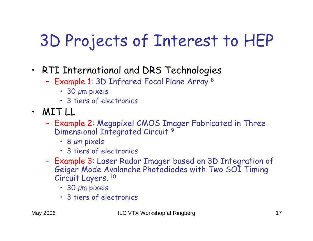
3D Projects of Interest to HEP• RTI International and DRS Technologies
– Example 1: 3D Infrared Focal Plane Array 8• 30 µm pixels• 3 tiers of electronics
• MIT LL– Example 2: Megapixel CMOS Imager Fabricated in Three
Dimensional Integrated Circuit 9• 8 µm pixels• 3 tiers of electronics
– Example 3: Laser Radar Imager based on 3D Integration of Geiger Mode Avalanche Photodiodes with Two SOI Timing Circuit Layers. 10
• 30 µm pixels• 3 tiers of electronics

May 2006 ILC VTX Workshop at Ringberg 18
3D Infrared Focal Plane Array• 256 x 256 array with
30 µm pixels• 3 Tiers
– HgCdTe (sensor)– 0.25 µm CMOS
(analog)– 0.18 µm CMOS
(digital)• Die to wafer stacking• Polymer adhesive
bonding• Bosch process vias (4
µm) with insulated side walls
• 99.98% good pixels• High diode fill factor
3 Tier circuit diagram
Infrared image
Array cross section
Synchronous Charge Removal
+
-+
-
ControlLogic
N BitRipple
Counter. . .
N Bit ParallelDigital Data Out
VCHG
VTRP
VRST
Cint
Cchg
CLK
CTIAOUT
Analog Residual Output
Detector
Analog Components Digital Components
Synchronous Charge Removal
+
-+
-
ControlLogic
N BitRipple
Counter. . .
N Bit ParallelDigital Data Out
VCHG
VTRP
VRST
Cint
Cchg
CLK
CTIAOUT
Analog Residual Output
Detector
Analog Components Digital Components
Diodes0.25 µmCMOS0.18 µmCMOS
Diode
Analog Digital
30 um
May 2006 ILC VTX Workshop at Ringberg 19
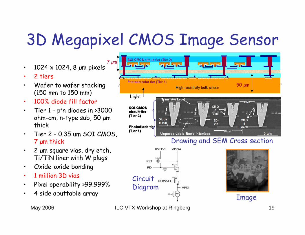
3D Megapixel CMOS Image Sensor • 1024 x 1024, 8 µm pixels• 2 tiers• Wafer to wafer stacking
(150 mm to 150 mm)• 100% diode fill factor• Tier 1 - p+n diodes in >3000
ohm-cm, n-type sub, 50 µm thick
• Tier 2 – 0.35 um SOI CMOS, 7 µm thick
• 2 µm square vias, dry etch, Ti/TiN liner with W plugs
• Oxide-oxide bonding• 1 million 3D vias• Pixel operability >99.999%• 4 side abuttable array
50 µm
7 µm
Drawing and SEM Cross section
CircuitDiagram
Image
Light

May 2006 ILC VTX Workshop at Ringberg 20
3D Laser Radar Imager• 64 x 64 array, 30 µm pixels• 3 tiers
– 0.18µm SOI– 0.35 µm SOI– High resistivity substrate
diodes• Oxide to oxide wafer bonding• 1.5 µm vias, dry etch• Six 3D vias per pixel
Tier 1
Tier 2
Tier 3
7 µm
7 µm
SEM Cross section
CAD DrawingSchematic

May 2006 ILC VTX Workshop at Ringberg 21
Four Ongoing Initiatives at Fermilab
• Investigate 3D thinning and bonding techniques with existing CMOS devices– BTEV pixel (FPIX) readout chips– BTEV pixel detectors
• Participate in 3 tier multi-project run – Design prototype pixel array with full readout for
ILC• Fabricate thin “edgeless” sensor array• Work with industry to develop diodes on high
resistivity substrate and pixel readout circuit in 0.18 um SOI.
May 2006 ILC VTX Workshop at Ringberg 22
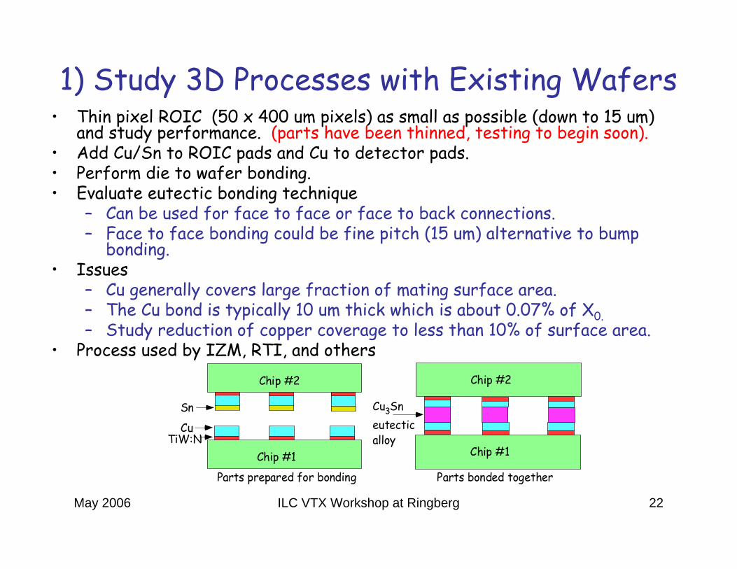
1) Study 3D Processes with Existing Wafers• Thin pixel ROIC (50 x 400 um pixels) as small as possible (down to 15 um)
and study performance. (parts have been thinned, testing to begin soon).• Add Cu/Sn to ROIC pads and Cu to detector pads.• Perform die to wafer bonding.• Evaluate eutectic bonding technique
– Can be used for face to face or face to back connections.– Face to face bonding could be fine pitch (15 um) alternative to bump
bonding.• Issues
– Cu generally covers large fraction of mating surface area.– The Cu bond is typically 10 um thick which is about 0.07% of X0.– Study reduction of copper coverage to less than 10% of surface area.
• Process used by IZM, RTI, and others
TiW:NCu
Sn
Parts prepared for bonding
Chip #1
Chip #2
Cu3Sneutecticalloy
Parts bonded together
Chip #2
Chip #1

May 2006 ILC VTX Workshop at Ringberg 23
2) Design of Pixel Readout Chip for ILC
• ILC Maximum hit occupancy– Assumed to be 0.03 particles/crossing/mm2
– Assume 3 hits pixels/particle (obviously this depends somewhat on pixel size and charge spreading)
– Hit rate = 0.03 part./bco/mm2 x 3 hits/part. x 2820 bco/train = 252 hits/train/mm2. 11
• Propose digital read out approach– Want better than 5 µm resolution– A square 15µm cell gives 15/3.46 = 4.3 µm.
May 2006 ILC VTX Workshop at Ringberg 24
Sparsification and Time Stamping
• Sparsification is highly desirable to reduce the volume of data being transmitted off any chip and to reduce the digital power dissipated in the chip.
• Although the occupancy is relatively low, Time Stamping is necessary to define when a hit in a given area occurred in order to reconstruct a hit pattern in association with data from other detectors.

May 2006 ILC VTX Workshop at Ringberg 25
Required Pipeline Depth• Occupancy for single 15 µm x 15 µm pixel
– Occupancy = 250 hits/mm2 (15µm x 15µm)= 0.056 hits/bunch train
– Chance of a single cell being hit twice in a bunch train = .056 x .056 = .0031 = 0.3%
– Therefore, with a depth of only one, 99.7% of hits are recorded unambiguously.
• For comparison, occupancy in a 4 x4 array of 15 um pixels would require a 3 deep time stamp buffer and provide 98.6% efficiency.

May 2006 ILC VTX Workshop at Ringberg 26
Chip Design Choices• Use token passing scheme developed for BTEV pixel
and silicon strip RO chips to sparsify data output.• Divide the bunch train into 32 time slices. Each pixel
stores one time stamp equivalent to 5 bits of time information.
• Do not store pixel addresses in the pixel cell.• Store the time stamp in the hit pixel cell.• Minimize number of transistors/pixel as much as
possible.• For time being, consider independent pixel cell
processing. Multiple cell processing (cell grouping) on multiple tiers could reduce the overall transistor count.
May 2006 ILC VTX Workshop at Ringberg 27
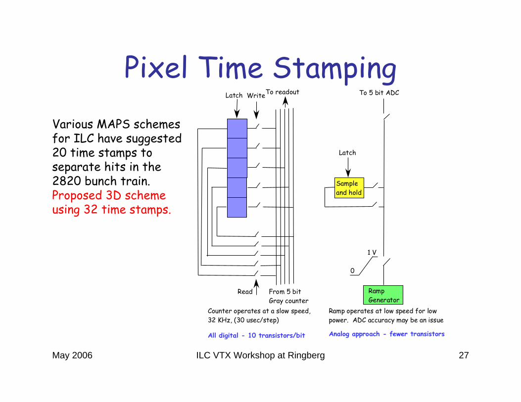
Pixel Time StampingVarious MAPS schemes for ILC have suggested 20 time stamps to separate hits in the 2820 bunch train. Proposed 3D scheme using 32 time stamps.
Read
Latch Write
All digital - 10 transistors/bit
To readout
From 5 bitGray counter
Counter operates at a slow speed,32 KHz, (30 usec/step)
RampGenerator
Sampleand hold
Latch
To 5 bit ADC
0
1 V
Ramp operates at low speed for lowpower. ADC accuracy may be an issue
Analog approach - fewer transistors

May 2006 ILC VTX Workshop at Ringberg 28
Sparsified Readout Concept
X=1
T11 5
Y=1
X=2
T21 5
10 10
Y=2
Y=3
Y address bus
110
cell1:1
cell2:1
cell1:2
cell2:2
cell1:3
X=1000
Token to row Y=2
Token to row Y=3
Serial Data out(30 bits/hit)
Data MuxX,Y,T
StartReadoutToken
XYT
T1buf T2buf
Note: All the Y address registers can be replaced by one counter thatis incremented by the last column token.
cell1000:1
cell2:3
cell1000:2
cell1000:3

May 2006 ILC VTX Workshop at Ringberg 29
Sparsified Readout• During acquisition, a hit sets a latch.• Sparse readout performed row by row.• To start readout, all hit pixels are disabled except
the first hit pixel in the readout scan.• The pixel being read points to the X address and Y
address stored on the perimeter and at the same time outputs the Time Stamp information from the pixel.
• While reading out first address and time stamp, a token scans ahead looking for next pixel to readout.
• Chip set to always readout all pixels with X=1 address and last pixel in the array.
• Assume 1000 x 1000 array (1000 pixels/row)– Time to scan 1 row = .125 ns x 1000 = 125 ns (TSMC 0.25um)– Time to readout cell = 30 bits x 20 ns/bit = 600 ns– Plenty of time to find next hit pixel during readout

May 2006 ILC VTX Workshop at Ringberg 30
Readout Time• Chip size = 1000 x 1000 pixels with 15 um pixels.• Max hits/chip = 250 hits/mm2 x 225 mm2 = 56250
hits/chip.• If you read all pixels with X=1, add 1000 pixels (small
increase in readout data).• For 50 MHz readout clock and 30 bits/hit, readout
time = 57250 hits x 30 bits/hit x 20 ns/bit = 34 msec.• Readout time is far less than the ILC allowed 200
msec. Thus the readout clock can be even slower or several chips can be put on the same bus.
• If CMOS is used, the output power is only dependent on the number of bits and not the length of time needed to readout.

May 2006 ILC VTX Workshop at Ringberg 31
Pixel Cell Block Diagram
Sensing diode
Amp Disc
10T 7T
Tier 1 - 17 Transistors
1 via
KillS.R.
HitLatch Token
pass
Token in Token out
To X addressregister
To Y address register
Time stampregister
51
5T
8T
20 T
Tier 2 - 37 Transistors Tier 3 - 50 Transistors
2 Vias
To Time stampregister
4T
Reset
2 phase clock
In Out

May 2006 ILC VTX Workshop at Ringberg 32
3D Advantages• High resistivity substrate for diodes• Minimum charge spreading with fully depleted
substrate• 100% diode fill factor• No limitation on PMOS usage• SOI for low power• Increased circuit density without going to
smaller feature sizes• 3D may be used to add layers above other
MAPS currently under development.

May 2006 ILC VTX Workshop at Ringberg 33
Chip FabricationFabricate Chip in MIT LLMultiproject run, Oct 1, 2006.Reticule from previous Multi-project run shown below
Multi-project run has 3 tiers eachwith 3 metal layers (3 transistor levels, 11 metal layers)
~7 um
~7 um
~7 um
Bond
Bond
Tier 1
Tier 2
Tier 3

May 2006 ILC VTX Workshop at Ringberg 34
Process flow for 3D Chip• 3 tier chip (tier 1 may
be CMOS)– 0.18 um (all layers)– SOI simplifies via
formation• Single vendor
processing
1) Fabricate individual tiers
2) Invert, align, and bond wafer 2 to wafer 1
3) Remove handle silicon from wafer 2, etch 3D Vias, deposit and CMP tungsten
4) Invert, align and bond wafer 3 to wafer 2/1 assembly, remove wafer 3 handle wafer, form3D vias from tier 2 to tier 3
Oxidebond
3DVia

May 2006 ILC VTX Workshop at Ringberg 35
3) Pixel Sensor Development• Develop sensor for 3D or bump bonded applications
– Sensor thickness: 50 to 100 µm– Pixel to detector edge ~ 15 µm– 3000 ohm-cm material– 15-20 µm pitch– Four side abuttable
• Trench etch edges (4 µm x 50 µm, Bosch process), • Fill trench with doped glass (PSG), drive into silicon• Backside PSG (phosphor) implant followed by laser annealing
• Initially to be mated to 3D ROIC• Fabricate at MIT LL by December 2006, (room for others to
participate in sensor run)
n substrate
p+
n+
May 2006 ILC VTX Workshop at Ringberg 36
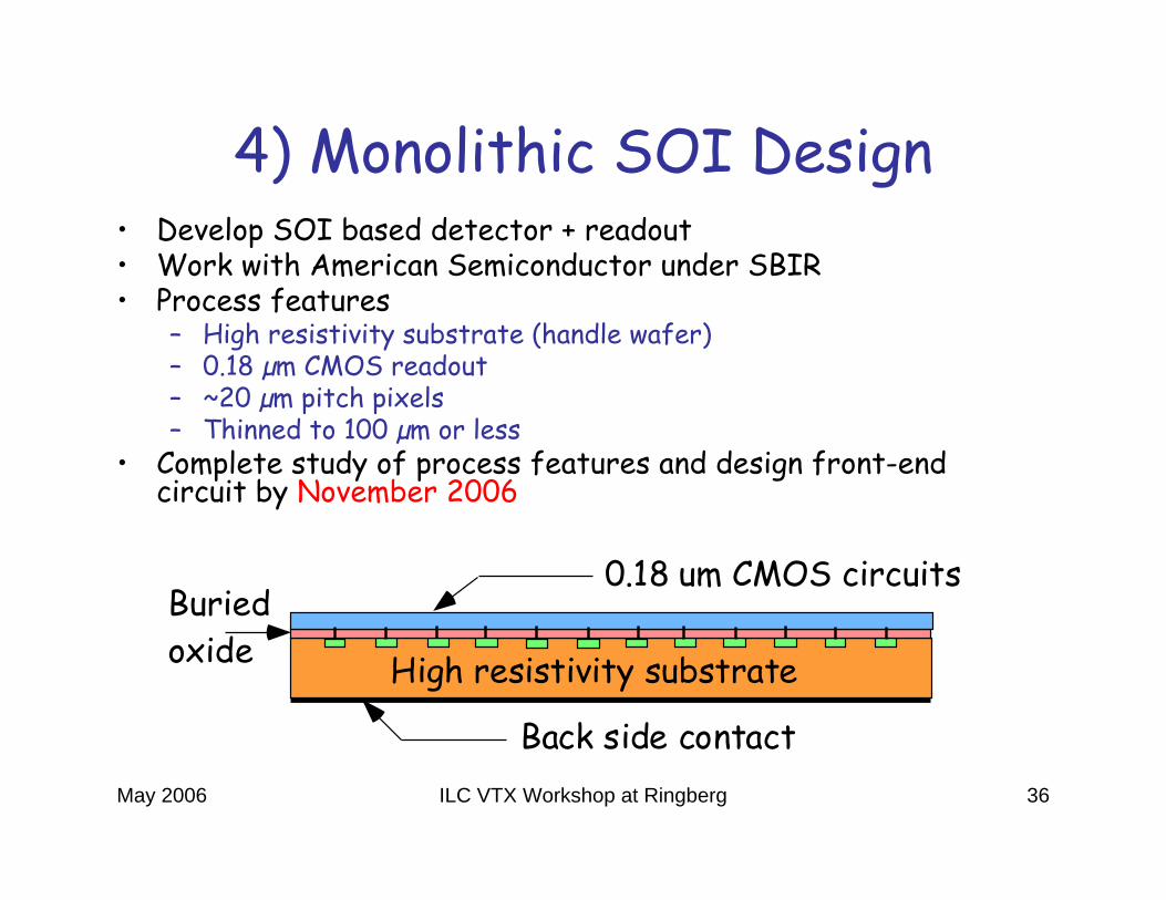
4) Monolithic SOI Design• Develop SOI based detector + readout• Work with American Semiconductor under SBIR• Process features
– High resistivity substrate (handle wafer)– 0.18 µm CMOS readout – ~20 µm pitch pixels– Thinned to 100 µm or less
• Complete study of process features and design front-end circuit by November 2006
High resistivity substrate
Buriedoxide
0.18 um CMOS circuits
Back side contact
May 2006 ILC VTX Workshop at Ringberg 37
Conclusion• Several initiatives for the ILC pixel detector are being
pursued at Fermilab.• Two different 3D electronics approaches are being
studied– Working with existing wafers
• Thinning• Bonding
– Complete new design for 3D IC• Two different detector efforts are under way
– Develop thin, edgeless sensor for abuttable arrays– Develop sensor and readout circuit in SOI
• 3D may open new opportunities for HEP• 3D may be used as an add-on for current MAPS work

May 2006 ILC VTX Workshop at Ringberg 38
References1) 3D Architectures for Semiconductor Integration and Packaging Conference,
June 2005, Tempe Arizona.2) “Introduction to 3D Integration”, Kerry Bernstein, IBM, ISSCC 2006.3) “Pixelated Architectures: Drives for 3D Integration Techniques”, Ken Williams,
3D Architectures for Semiconductor Integration and Packaging, June 2005, Tempe Arizona.
4) “Future ICs Go Vertical”, Philip Garrou, Semiconductor International, February 1, 2005.
5) “Impact of ultra-thinning on DC Characteristics of MOSFET Devices”, S. Pinel,et. al., Eur. Phys. J. AP 17, 41-43, 2002.
6) “Characterization of Fully Depleted SOI Transistors after Removal of the Silicon Substrate”, J. Burns, et. al., IEEE SOI Conference 2001.
7) “Through-Wafer Via Etching”, A. Chambers, et. al., Advanced Packaging,April 2005.
8) “3-D Integration Technology Platform for High Performance Detector Arrays”,D. Temple, et. al., public release from RTI International and DRS Technologies.
9) “Megapixel CMOS Image Sensor Fabricate in Three-Dimensional IntegratedCircuit Technology”, V. Suntharalingam, et. al., ISSCC 2005, pp 356-357.
10) Laser Radar Imager Based on 3D Integration of Geiger-Mode AvalanchePhotodiodes with Two SOI Timing Circuit layers”, B. Aull, et. al., ISSCC 2006, pp 26-27.
11) Monolithic CMOS Pixel Detectors for ILC Vertex Detection”, C. Baltay, et. al., ILC Workshop, April 3, 2006.