features - sitime
TRANSCRIPT

SiT5157
60 MHz to 220 MHz, ±0.5 to ±2.5 ppm, Elite Platform™ Super-TCXO
Description
The SiT5157 is a ±0.5 ppm to ±2.5 ppm MEMS Super-TCXO
that is engineered for best dynamic performance. It is ideal
for high reliability telecom, wireless and networking,
industrial, precision GNSS and audio/video applications.
Leveraging SiTime’s unique DualMEMS™ temperature
sensing and TurboCompensation™ technologies, the
SiT5157 delivers the best dynamic performance for timing
stability in the presence of environmental stressors such as
air flow, temperature perturbation, vibration, shock, and
electromagnetic interference. This device also integrates
multiple on-chip regulators to filter power supply noise,
eliminating the need for a dedicated external LDO.
The SiT5157 offers three device configurations that can be
ordered using Ordering Codes for:
The SiT5157 can be factory programmed for any
combination of frequency, stability, voltage, and pull range.
Programmability enables designers to optimize clock
configurations while eliminating long lead times and
customization costs associated with quartz devices where
each frequency is custom built.
Refer to Manufacturing Guideline for proper reflow profile
and PCB cleaning recommendations for best performance.
Features
◼ Output 60–189 MHz, and 208–220 MHz, in 1 Hz steps
◼ Factory programmable options for short lead time
◼ Best dynamic stability under airflow, thermal shock
±0.5 ppm stability across temperature
±15 ppb/°C typical frequency slope (ΔF/ΔT)
◼ -40°C to +105°C operating temperature
◼ No activity dips or micro jumps
◼ Resistant to shock, vibration and board bending
◼ On-chip regulators eliminate the need for external LDOs
◼ Digital frequency pulling (DCTCXO) via I2C
Digital control of output frequency and pull range
Up to ±3200 ppm pull range
Frequency pull resolution down to 5 ppt
◼ 2.5 V, 2.8 V, 3.0 V and 3.3 V supply voltage
◼ LVCMOS output
◼ RoHS and REACH compliant,
◼ Pb-free, Halogen-free, Antimony-free
Applications
◼ Precision GNSS systems
◼ Microwave backhaul
◼ Network routers and switches
◼ Professional audio and video equipment
◼ Storage and servers
◼ Test and measurement
Block Diagram
Figure 1. SiT5157 Block Diagram
5.0 mm x 3.2 mm Package Pinout
OE / VC / NC 1
2
3
4 5 6
7
8
910
SCL / NC
NC
GND
NC
NC
VDD
CLK
A0 / NC
SDA / NC
Figure 2. Pin Assignments (Top view)
(Refer to Table 11 for Pin Descriptions)
Rev 1.06 November 4, 2021 www.sitime.com

SiT5157 60 MHz to 220 MHz, ±0.5 to ±2.5 ppm, Elite Platform™ Super-TCXO
Rev 1.06 Page 2 of 33 www.sitime.com
Ordering Information
The part number guide illustrated below is for reference only, in which boxes identify order codes having more than one option.
To customize and build an exact part number, use the SiTime Part Number Generator. To validate the part number, use the
SiTime Part Number Decoder.
Frequency Stability
"K": for ±0.5 ppm
"A": for ±1.0 ppm
"D": for ±2.5 ppm
Part Family
Silicon Revision Letter
Pull Range – DCTCXO mode only
"T": ±6.25 ppm
"R": ±10 ppm
"Q": ±12.5 ppm
"M": ±25 ppm
"B": ±50 ppm
"C": ±80 ppm
"E": ±100 ppm
"F": ±125 ppm
"G": ±150 ppm
"H": ±200 ppm
"X": ±400 ppm
"L": ±600 ppm
"Y": ±800 ppm
"S": ±1200 ppm
"Z": ±1600 ppm
"U": ±3200 ppm
Supply Voltage
"25": 2.5 V ±10%
"28": 2.8 V ±10%
"30": 3.0 V ±10%
"33": 3.3 V ±10%
Pin 1 Function – DCTCXO mode only
"I": Output Enable
"J": No Connect, software OE control
Temperature Range
"I": Industrial, -40 to 85°C
"C": Extended Commercial, -20 to 70°C
"E": Extended Industrial, -40 to 105°C
Package Size "F": 5.0 mm x 3.2 mmPin 1 Function – TCXO mode only
"E": Output Enable
"N": No Connect
I2C Address Mode – DCTCXO mode only
“0”, “1”, “2”, “3”, “4”, “5”, “6”, “7”, “8”, “9”, “A”, “B”,
“C”, “D”, “E”, “F”: Order code representing hex
value of I2C address. When the I
2C address is
factory programmed using this code, pin A0 is no
connect (NC).
“G”: I2C pin addressable mode. Address is set by
the logic on A0 pin.
Packaging
"T": 12 mm Tape & Reel, 3 ku reel
"Y": 12 mm Tape & Reel, 1 ku reel
“X”: 12 mm Tape & Reel, 250 u reel
(blank): bulk[2]
Frequency
60.000001 MHz to 189.000000 MHz
208.000000 MHz to 220.000000 MHz
Output Waveform "-" : LVCMOS[1]
SiT5157AC - FK - 33 E 0 - 98.123456 T
SiT5157AC - FK - 33 V T - 98.123456 T
SiT5157AC - FKG33 J R - 98.123456 T
TCXO
VCTCXO
DCTCXO
Notes: 1. “-“ corresponds to the default rise/fall time for LVCMOS output as specified in Table 1 (Electrical Characteristics). Contact SiTime for other rise/fall time
options for best EMI or driving multiple loads. For differential outputs, contact SiTime.
2. Bulk is available for sampling only.
SiT5157 60 MHz to 220 MHz, ±0.5 to ±2.5 ppm, Elite Platform™ Super-TCXO
Rev 1.06 Page 3 of 33 www.sitime.com
TABLE OF CONTENTS
Description........................................................................................................................................................................... 1 Features .............................................................................................................................................................................. 1 Applications ......................................................................................................................................................................... 1 Block Diagram ..................................................................................................................................................................... 1 5.0 mm x 3.2 mm Package Pinout ........................................................................................................................................ 1 Ordering Information ............................................................................................................................................................ 2 Electrical Characteristics ...................................................................................................................................................... 4 Device Configurations and Pin-outs ...................................................................................................................................... 8
Pin-out Top Views ......................................................................................................................................................... 8 Test Circuit Diagrams for LVCMOS Outputs .......................................................................................................................... 9 Waveforms ........................................................................................................................................................................ 10 Timing Diagrams ................................................................................................................................................................ 10 Typical Performance Plots .................................................................................................................................................. 11 Architecture Overview ........................................................................................................................................................ 12
Frequency Stability .......................................................................................................................................................12 Output Frequency and Format ......................................................................................................................................12 Output Frequency Tuning .............................................................................................................................................12 Pin 1 Configuration (OE, VC, or NC) .............................................................................................................................13
Device Configurations ........................................................................................................................................................ 13 TCXO Configuration .....................................................................................................................................................13 VCTCXO Configuration ................................................................................................................................................14 DCTCXO Configuration ................................................................................................................................................15
VCTCXO-Specific Design Considerations ........................................................................................................................... 16 Linearity .......................................................................................................................................................................16 Control Voltage Bandwidth ...........................................................................................................................................16 FV Characteristic Slope KV ...........................................................................................................................................16 Pull Range, Absolute Pull Range ..................................................................................................................................17
DCTCXO-Specific Design Considerations ........................................................................................................................... 18 Pull Range and Absolute Pull Range .............................................................................................................................18 Output Frequency.........................................................................................................................................................19 I2C Control Registers ....................................................................................................................................................21 Register Descriptions ...................................................................................................................................................21 Register Address: 0x00. Digital Frequency Control Least Significant Word (LSW) ..........................................................21 Register Address: 0x01. OE Control, Digital Frequency Control Most Significant Word (MSW) ........................................22 Register Address: 0x02. DIGITAL PULL RANGE CONTROL[15] .....................................................................................23 Serial Interface Configuration Description ......................................................................................................................24 Serial Signal Format .....................................................................................................................................................24 Parallel Signal Format ..................................................................................................................................................25 Parallel Data Format.....................................................................................................................................................25 I2C Timing Specification ................................................................................................................................................27 I2C Device Address Modes ...........................................................................................................................................28 Schematic Example ......................................................................................................................................................29
Dimensions and Patterns.................................................................................................................................................... 30 Layout Guidelines .............................................................................................................................................................. 31 Manufacturing Guidelines ................................................................................................................................................... 31 Additional Information ......................................................................................................................................................... 32 Revision History ................................................................................................................................................................. 33
SiT5157 60 MHz to 220 MHz, ±0.5 to ±2.5 ppm, Elite Platform™ Super-TCXO
Rev 1.06 Page 4 of 33 www.sitime.com
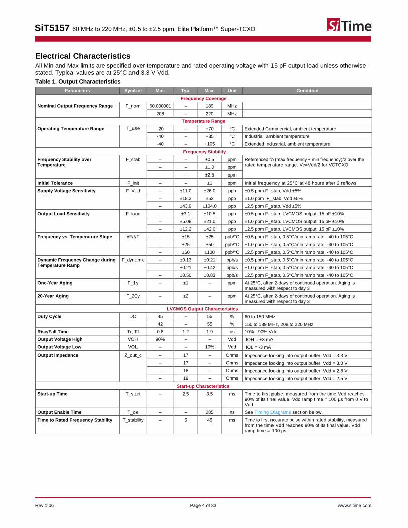
Electrical Characteristics All Min and Max limits are specified over temperature and rated operating voltage with 15 pF output load unless otherwise stated. Typical values are at 25°C and 3.3 V Vdd.
Table 1. Output Characteristics
Parameters Symbol Min. Typ. Max. Unit Condition
Frequency Coverage
Nominal Output Frequency Range F_nom 60.000001 – 189 MHz
208 – 220 MHz
Temperature Range
Operating Temperature Range T_use -20 – +70 °C Extended Commercial, ambient temperature
-40 – +85 °C Industrial, ambient temperature
-40 – +105 °C Extended Industrial, ambient temperature
Frequency Stability
Frequency Stability over Temperature
F_stab – – ±0.5 ppm Referenced to (max frequency + min frequency)/2 over the rated temperature range. Vc=Vdd/2 for VCTCXO
– – ±1.0 ppm
– – ±2.5 ppm
Initial Tolerance F_init – – ±1 ppm Initial frequency at 25°C at 48 hours after 2 reflows
Supply Voltage Sensitivity F_Vdd – ±11.0 ±26.0 ppb ±0.5 ppm F_stab, Vdd ±5%
– ±18.3 ±52 ppb ±1.0 ppm F_stab, Vdd ±5%
– ±43.9 ±104.0 ppb ±2.5 ppm F_stab, Vdd ±5%
Output Load Sensitivity F_load – ±3.1 ±10.5 ppb ±0.5 ppm F_stab. LVCMOS output, 15 pF ±10%
– ±5.08 ±21.0 ppb ±1.0 ppm F_stab. LVCMOS output, 15 pF ±10%
– ±12.2 ±42.0 ppb ±2.5 ppm F_stab. LVCMOS output, 15 pF ±10%
Frequency vs. Temperature Slope ΔF/ΔT – ±15 ±25 ppb/°C ±0.5 ppm F_stab, 0.5°C/min ramp rate, -40 to 105°C
– ±25 ±50 ppb/°C ±1.0 ppm F_stab, 0.5°C/min ramp rate, -40 to 105°C
– ±60 ±100 ppb/°C ±2.5 ppm F_stab, 0.5°C/min ramp rate, -40 to 105°C
Dynamic Frequency Change during Temperature Ramp
F_dynamic – ±0.13 ±0.21 ppb/s ±0.5 ppm F_stab, 0.5°C/min ramp rate, -40 to 105°C
– ±0.21 ±0.42 ppb/s ±1.0 ppm F_stab, 0.5°C/min ramp rate, -40 to 105°C
– ±0.50 ±0.83 ppb/s ±2.5 ppm F_stab, 0.5°C/min ramp rate, -40 to 105°C
One-Year Aging F_1y – ±1 – ppm At 25°C, after 2-days of continued operation. Aging is measured with respect to day 3
20-Year Aging F_20y – ±2 – ppm At 25°C, after 2-days of continued operation. Aging is measured with respect to day 3
LVCMOS Output Characteristics
Duty Cycle DC 45 – 55 % 60 to 150 MHz
42 – 55 % 150 to 189 MHz, 208 to 220 MHz
Rise/Fall Time Tr, Tf 0.8 1.2 1.9 ns 10% - 90% Vdd
Output Voltage High VOH 90% – – Vdd IOH = +3 mA
Output Voltage Low VOL – – 10% Vdd IOL = -3 mA
Output Impedance Z_out_c – 17 – Ohms Impedance looking into output buffer, Vdd = 3.3 V
– 17 – Ohms Impedance looking into output buffer, Vdd = 3.0 V
– 18 – Ohms Impedance looking into output buffer, Vdd = 2.8 V
– 19 – Ohms Impedance looking into output buffer, Vdd = 2.5 V
Start-up Characteristics
Start-up Time T_start – 2.5 3.5 ms Time to first pulse, measured from the time Vdd reaches 90% of its final value. Vdd ramp time = 100 µs from 0 V to Vdd
Output Enable Time T_oe – – 285 ns See Timing Diagrams section below.
Time to Rated Frequency Stability T_stability – 5 45 ms Time to first accurate pulse within rated stability, measured from the time Vdd reaches 90% of its final value. Vdd ramp time = 100 µs

SiT5157 60 MHz to 220 MHz, ±0.5 to ±2.5 ppm, Elite Platform™ Super-TCXO
Rev 1.06 Page 5 of 33 www.sitime.com
Table 2. DC Characteristics
Parameters Symbol Min. Typ. Max. Unit Condition
Supply Voltage
Supply Voltage
Vdd 2.25 2.5 2.75 V Contact SiTime for 2.25 V to 3.63 V continuous supply voltage support
2.52 2.8 3.08 V
2.7 3.0 3.3 V
2.97 3.3 3.63 V
Current Consumption
Current Consumption
Idd
– 48 62 mA F_nom = 100 MHz, No Load, TCXO and DCTCXO modes
– 52 66 mA F_nom = 100 MHz, No Load, VCTCXO mode
OE Disable Current
I_od
– 45 52 mA OE = GND, output weakly pulled down. TCXO, DCTCXO
– 49 56 mA OE = GND, output weakly pulled down. VCTCXO mode
Table 3. Input Characteristics
Parameters Symbol Min. Typ. Max. Unit Condition
Input Characteristics – OE Pin
Input Impedance Z_in 75 – – kΩ Internal pull up to Vdd
Input High Voltage VIH 70% – – Vdd
Input Low Voltage VIL – – 30% Vdd
Frequency Tuning Range – Voltage Control or I2C mode
Pull Range PR
±6.25 – – ppm VCTCXO mode; contact SiTime for ±12.5 and ±25 ppm
±6.25
±10
±12.5
±25
±50
±80
±100
±125
±150
±200
±400
±600
±800
±1200
±1600
±3200
– – ppm DCTCXO mode
Absolute Pull Range[3] APR ±2.75 – – ppm ±0.5 ppm F_stab, DCTCXO, VCTCXO for PR = ±6.25 ppm
±2.25 – – ppm ±1.0 ppm F_stab, DCTCXO, VCTCXO for PR = ±6.25 ppm
±0.75 – – ppm ±2.5 ppm F_stab, DCTCXO, VCTCXO for PR = ±6.25 ppm
Upper Control Voltage VC_U 90% – – Vdd VCTCXO mode
Lower Control Voltage VC_L – – 10% Vdd VCTCXO mode
Control Voltage Input Impedance VC_z 8 – – MΩ VCTCXO mode
Control Voltage Input Bandwidth VC_bw – 10 – kHz VCTCXO mode; contact SiTime for other bandwidth options
Frequency Control Polarity F_pol Positive VCTCXO mode
Pull Range Linearity PR_lin – 0.5 1.0 % VCTCXO mode
I2C Interface Characteristics, 200 Ohm, 550 pF (Max I2C Bus Load)
Bus Speed F_I2C ≤ 400 kHz -40 to 105°C
≤ 1000 kHz -40 to 85°C
Input Voltage Low VIL_I2C – – 30% Vdd DCTCXO mode
Input Voltage High VIH_I2C 70% – – Vdd DCTCXO mode
Output Voltage Low VOL_I2C – – 0.4 V DCTCXO mode
Input Leakage current IL 0.5 – 24 µA 0.1 VDD< VOUT < 0.9 VDD. Includes typical leakage current from 200 kΩ pull resister to VDD; DCTCXO mode
Input Capacitance CIN – – 5 pF DCTCXO mode
Note: 3. APR = PR – initial tolerance – 20-year aging – frequency stability over temperature. Refer to Table 14 for APR with respect to other pull range options.

SiT5157 60 MHz to 220 MHz, ±0.5 to ±2.5 ppm, Elite Platform™ Super-TCXO
Rev 1.06 Page 6 of 33 www.sitime.com
Table 4. Jitter & Phase Noise, -40°C to 85°C
Parameters Symbol Min. Typ. Max. Unit Condition
Jitter
RMS Phase Jitter (random) T_phj – 0.31 0.48 ps F_nom = 100 MHz, Integration bandwidth = 12 kHz to 20 MHz
RMS Period Jitter T_jitt_per – 1.0 1.8 ps F_nom = 100 MHz, population 10 k
Peak Cycle-to-Cycle Jitter T_jitt_cc – 6.6 13.4 ps F_nom = 100 MHz, population 1 k, measured as absolute value
Phase Noise
1 Hz offset – -61 -54 dBc/Hz
F_nom = 100 MHz TCXO and DCTCXO modes, and VCTCXO mode with ±6.25 ppm pull range
10 Hz offset – -89 -83 dBc/Hz
100 Hz offset – -107 -103 dBc/Hz
1 kHz offset – -128 -124 dBc/Hz
10 kHz offset – -133 -131 dBc/Hz
100 kHz offset – -133 -130 dBc/Hz
1 MHz offset – -150 -146 dBc/Hz
5 MHz offset – -157 -151 dBc/Hz
10 MHz offset – -157 -152 dBc/Hz
20 MHz offset – -159 -152 dBc/Hz
Spurious T_spur – -91 -86 dBc F_nom = 100 MHz, 1 kHz to 40 MHz offsets
Table 5. Jitter & Phase Noise, -40°C to 105°C
Parameters Symbol Min. Typ. Max. Unit Condition
Jitter
RMS Phase Jitter (random) T_phj – 0.31 0.50 ps F_nom = 100 MHz, Integration bandwidth = 12 kHz to 20 MHz
RMS Period Jitter T_jitt_per – 1.0 1.8 ps F_nom = 100 MHz, population 10 k
Peak Cycle-to-Cycle Jitter T_jitt_cc – 6.6 13.4 ps F_nom = 100 MHz, population 1 k, measured as absolute value
Phase Noise
1 Hz offset – -61 -54 dBc/Hz
F_nom = 100 MHz TCXO and DCTCXO modes, and VCTCXO mode with ±6.25 ppm pull range
10 Hz offset – -89 -83 dBc/Hz
100 Hz offset – -107 -103 dBc/Hz
1 kHz offset – -128 -124 dBc/Hz
10 kHz offset – -133 -131 dBc/Hz
100 kHz offset – -133 -130 dBc/Hz
1 MHz offset – -150 -144 dBc/Hz
5 MHz offset – -157 -150 dBc/Hz
10 MHz offset – -157 -150 dBc/Hz
20 MHz offset – -159 -150 dBc/Hz
Spurious T_spur – -91 -85 dBc F_nom = 100 MHz, 1 kHz to 40 MHz offsets

SiT5157 60 MHz to 220 MHz, ±0.5 to ±2.5 ppm, Elite Platform™ Super-TCXO
Rev 1.06 Page 7 of 33 www.sitime.com
Table 6. Absolute Maximum Limits
Attempted operation outside the absolute maximum ratings may cause permanent damage to the part. Actual performance of the IC is only guaranteed within the operational specifications, not at absolute maximum ratings.
Parameter Test Conditions Value Unit
Storage Temperature -65 to 125 °C
Continuous Power Supply Voltage Range (Vdd) -0.5 to 4 V
Human Body Model (HBM) ESD Protection JESD22-A114 2000 V
Soldering Temperature (follow standard Pb-free soldering guidelines) 260 °C
Junction Temperature[4] 130 °C
Input Voltage, Maximum Any input pin Vdd + 0.3 V
Input Voltage, Minimum Any input pin -0.3 V
Note: 4. Exceeding this temperature for an extended period of time may damage the device.
Table 7. Thermal Considerations[5]
Package JA[6] (°C/W) JC, Bottom (°C/W)
Ceramic 5.0 mm x 3.2 mm 54 15
Note: 5. Measured in still air. Refer to JESD51 for θJA and θJC definitions.
6. Devices soldered on a JESD51 2s2p compliant board.
Table 8. Maximum Operating Junction Temperature[7]
Max Operating Temperature (ambient) Maximum Operating Junction Temperature
70°C 80°C
85°C 95°C
105°C 115°C
Note: 7. Datasheet specifications are not guaranteed if junction temperature exceeds the maximum operating junction temperature.
Table 9. Environmental Compliance
Parameter Test Conditions Value Unit
Mechanical Shock Resistance MIL-STD-883F, Method 2002 30000 g
Mechanical Vibration Resistance MIL-STD-883F, Method 2007 70 g
Temperature Cycle JESD22, Method A104 – –
Solderability MIL-STD-883F, Method 2003 – –
Moisture Sensitivity Level MSL1 @260°C – –

SiT5157 60 MHz to 220 MHz, ±0.5 to ±2.5 ppm, Elite Platform™ Super-TCXO
Rev 1.06 Page 8 of 33 www.sitime.com
Device Configurations and Pin-outs
Table 10. Device Configurations
Configuration Pin 1 Pin 5 I2C Programmable Parameters
TCXO OE/NC NC –
VCTCXO VC NC –
DCTCXO OE/NC A0/NC Frequency Pull Range, Frequency Pull Value, Output Enable control.
Pin-out Top Views
OE/NC 1
2
3
4 5 6
7
8
910
NC
NC
GND
NC
NC
VDD
CLK
NC
NC
Figure 3. TCXO
VC 1
2
3
4 5 6
7
8
910
NC
NC
GND
NC
NC
VDD
CLK
NC
NC
Figure 4. VCTCXO
OE / NC 1
2
3
4 5 6
7
8
910
SCL
NC
GND
NC
NC
VDD
CLK
A0 / NC
SDA
Figure 5. DCTCXO
Table 11. Pin Description
Pin Symbol I/O Internal Pull-up/Pull Down
Resistor Function
1 OE/NC[10]/VC
OE – Input 100 kΩ Pull-Up H[8]: specified frequency output L: output is high impedance. Only output driver is disabled.
NC – No Connect – H or L or Open: No effect on output frequency or other device functions
VC – Input – Control Voltage in VCTCXO Mode
2 SCL / NC[10] SCL – Input 200 kΩ Pull-Up I2C serial clock input.
No Connect H or L or Open: No effect on output frequency or other device functions
3 NC[10] No Connect – H or L or Open: No effect on output frequency or other device functions
4 GND Power – Connect to ground
5 A0 / NC[10] A0 – Input 100 kΩ Pull-Up
Device I2C address when the address selection mode is via the A0 pin. This pin is NC when the I2C device address is specified in the ordering
code.
A0 Logic Level I2C Address
0 1100010
1 1101010
NC – No Connect – H or L or Open: No effect on output frequency or other device functions.
6 CLK Output – LVCMOS
7 NC[10] No Connect – H or L or Open: No effect on output frequency or other device functions
8 NC[10] No Connect – H or L or Open: No effect on output frequency or other device functions
9 VDD Power – Connect to power supply[9]
10 SDA / NC [10] SDA – Input/Output 200 kΩ Pull Up I2C Serial Data.
NC – No Connect – H or L or Open: No effect on output frequency or other device functions.
Notes:
8. In OE mode for noisy environments, a pull-up resistor of 10 kΩ or less is recommended if pin 1 is not externally driven. If pin 1 needs to be left floating, use
the NC option.
9. A 0.1 μF capacitor in parallel with a 10 μF capacitor are required between VDD and GND. The 0.1 μF capacitor is recommended to place close to the device,
and place the 10 μF capacitor less than 2 inches away.
10. All NC pins can be left floating and do not need to be soldered down.
SiT5157 60 MHz to 220 MHz, ±0.5 to ±2.5 ppm, Elite Platform™ Super-TCXO
Rev 1.06 Page 9 of 33 www.sitime.com
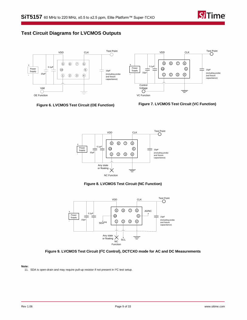
Test Circuit Diagrams for LVCMOS Outputs
9 8 7 6
1 2 3 4
510Power
Supply
VDDTest Point
Vdd
OE Function
CLK
15pF
(including probe
and fixture
capacitance)
10µF
0.1µF+
-
10µF
0.1µF+
-
9 8 7 6
1 2 3 4
510Power
Supply
VDDTest Point
Control
Voltage
VC Function
CLK
15pF
(including probe
and fixture
capacitance)
Figure 6. LVCMOS Test Circuit (OE Function)
Figure 7. LVCMOS Test Circuit (VC Function)
9 8 7 6
1 2 3 4
510Power
Supply
VDDTest Point
Any state
or floating
NC Function
CLK
15pF
(including probe
and fixture
capacitance)
10µF
0.1µF+
-
Figure 8. LVCMOS Test Circuit (NC Function)
9 8 7 6
1 2 3 4
510Power
Supply
VDDTest Point
Any state
or floating
NC
Function
CLK
SCL
SDA[11]
15pF
(including probe
and fixture
capacitance)
10µF
0.1µF+
-
A0/NC
Figure 9. LVCMOS Test Circuit (I2C Control), DCTCXO mode for AC and DC Measurements
Note: 11. SDA is open-drain and may require pull-up resistor if not present in I2C test setup.

SiT5157 60 MHz to 220 MHz, ±0.5 to ±2.5 ppm, Elite Platform™ Super-TCXO
Rev 1.06 Page 10 of 33 www.sitime.com
Waveforms
90 % Vdd
50 % Vdd
10 % Vdd
tr tf
High Pulse
(TH)
Low Pulse
(TL)
Period
Figure 10. LVCMOS Waveform Diagram[12]
Note: 12. Duty Cycle is computed as Duty Cycle = TH/Period.
Timing Diagrams
90% VddVdd
Vdd Pin
Voltage
CLK Output
T_start
T_start: Time to start from power-off
HZ
Figure 11. Startup Timing
50% Vdd
Vdd
OE Voltage
CLK Output
T_oe
T_oe: Time to re-enable the clock output
HZ
Figure 12. OE Enable Timing (OE Mode Only)

SiT5157 60 MHz to 220 MHz, ±0.5 to ±2.5 ppm, Elite Platform™ Super-TCXO
Rev 1.06 Page 11 of 33 www.sitime.com
Typical Performance Plots
Figure 13. Duty Cycle (LVCMOS)
Figure 14. IDD DCTCXO (LVCMOS)
Figure 15. IDD TCXO (LVCMOS)
Figure 16. IDD VCTCXO (LVCMOS)
Figure 17. RMS Phase Jitter, DCTCXO, TCXO (LVCMOS)
Figure 18. RMS Period Jitter (LVCMOS)
Figure 19. RMS Phase Jitter, VCTCXO (LVCMOS)
Figure 20. DCTCXO frequency pull characteristic
45
47
49
51
53
55
70 90 110 130 150 170 190 210
Du
ty c
ycle
(%
)
Frequency (MHz)
2.5 V 2.8 V 3.0 V 3.3 V
40
42
44
46
48
50
52
54
56
58
70 90 110 130 150 170 190 210
Cu
rre
nt
con
sum
pti
on
(m
A)
Frequency (MHz)
2.5 V 2.8 V 3.0 V 3.3 V
40
42
44
46
48
50
52
54
56
58
70 90 110 130 150 170 190 210
Cu
rre
nt
con
sum
pti
on
(m
A)
Frequency (MHz)
2.5 V 2.8 V 3.0 V 3.3 V
46
48
50
52
54
56
58
60
70 90 110 130 150 170 190 210
Cu
rre
nt
con
sum
pti
on
(m
A)
Frequency (MHz)
2.5 V 2.8 V 3.0 V 3.3 V
0
100
200
300
400
500
70 90 110 130 150 170 190 210
Ph
ase
Jit
ter
(fs
RM
S)
Frequency (MHz)
2.5 V 2.8 V 3.0 V 3.3 V
0.50
0.70
0.90
1.10
1.30
1.50
1.70
1.90
70 90 110 130 150 170 190 210
Pe
rio
d J
itte
r (p
s R
MS)
Frequency (MHz)
2.5 V 3.3 V
0
100
200
300
400
500
70 120 170 220
Ph
ase
Jit
ter
(fs
RM
S)
Frequency (MHz)
2.5 V 2.8 V 3.0 V 3.3 V
-6.25
-5
-3.75
-2.5
-1.25
0
1.25
2.5
3.75
5
6.25
-6.25 -5 -3.75 -2.5 -1.25 0 1.25 2.5 3.75 5 6.25
Fre
qu
en
cy d
evi
atio
n (
pp
m)
DCTCXO pull (ppm)
SiT5157 60 MHz to 220 MHz, ±0.5 to ±2.5 ppm, Elite Platform™ Super-TCXO
Rev 1.06 Page 12 of 33 www.sitime.com
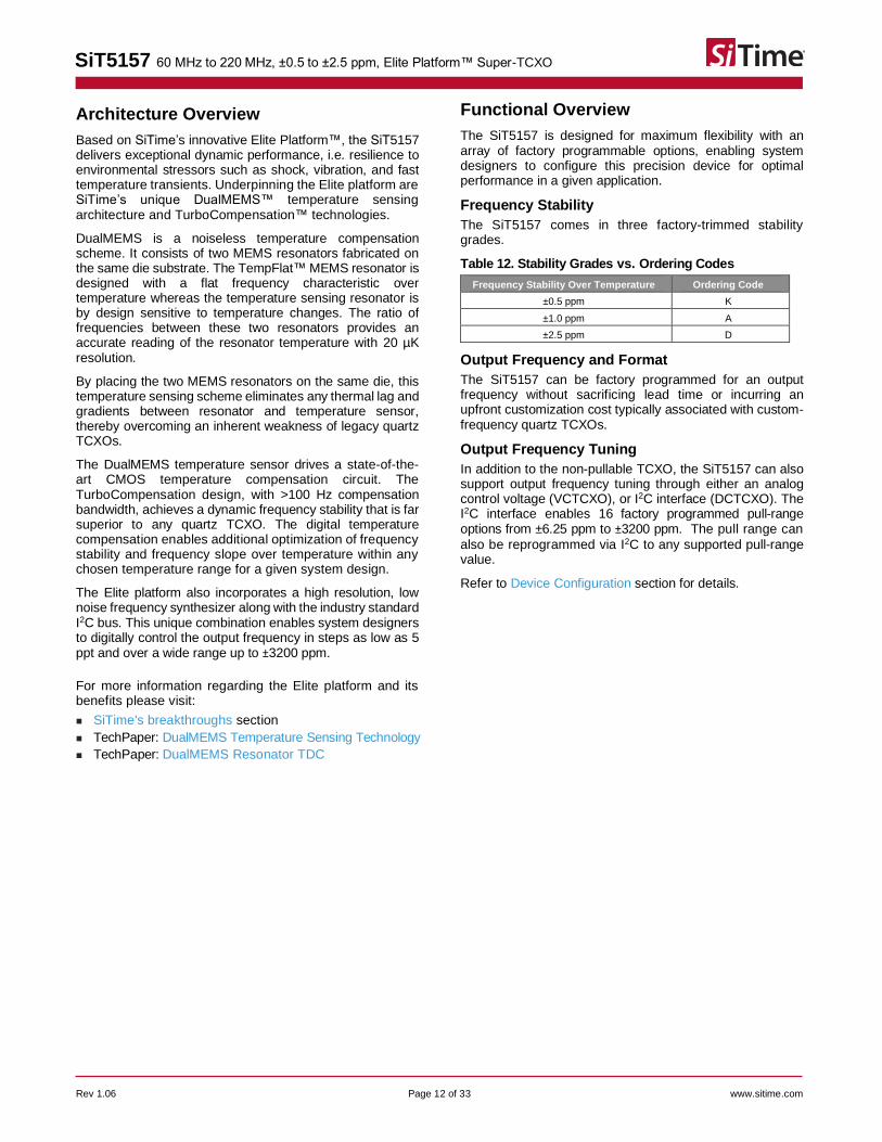
Architecture Overview
Based on SiTime’s innovative Elite Platform™, the SiT5157 delivers exceptional dynamic performance, i.e. resilience to environmental stressors such as shock, vibration, and fast temperature transients. Underpinning the Elite platform are SiTime’s unique DualMEMS™ temperature sensing architecture and TurboCompensation™ technologies.
DualMEMS is a noiseless temperature compensation scheme. It consists of two MEMS resonators fabricated on the same die substrate. The TempFlat™ MEMS resonator is designed with a flat frequency characteristic over temperature whereas the temperature sensing resonator is by design sensitive to temperature changes. The ratio of frequencies between these two resonators provides an accurate reading of the resonator temperature with 20 µK resolution.
By placing the two MEMS resonators on the same die, this temperature sensing scheme eliminates any thermal lag and gradients between resonator and temperature sensor, thereby overcoming an inherent weakness of legacy quartz TCXOs.
The DualMEMS temperature sensor drives a state-of-the-art CMOS temperature compensation circuit. The TurboCompensation design, with >100 Hz compensation bandwidth, achieves a dynamic frequency stability that is far superior to any quartz TCXO. The digital temperature compensation enables additional optimization of frequency stability and frequency slope over temperature within any chosen temperature range for a given system design.
The Elite platform also incorporates a high resolution, low noise frequency synthesizer along with the industry standard I2C bus. This unique combination enables system designers to digitally control the output frequency in steps as low as 5 ppt and over a wide range up to ±3200 ppm.
For more information regarding the Elite platform and its benefits please visit:
◼ SiTime's breakthroughs section
◼ TechPaper: DualMEMS Temperature Sensing Technology
◼ TechPaper: DualMEMS Resonator TDC
Functional Overview
The SiT5157 is designed for maximum flexibility with an array of factory programmable options, enabling system designers to configure this precision device for optimal performance in a given application.
Frequency Stability
The SiT5157 comes in three factory-trimmed stability grades.
Table 12. Stability Grades vs. Ordering Codes
Frequency Stability Over Temperature Ordering Code
±0.5 ppm K
±1.0 ppm A
±2.5 ppm D
Output Frequency and Format
The SiT5157 can be factory programmed for an output frequency without sacrificing lead time or incurring an upfront customization cost typically associated with custom-frequency quartz TCXOs.
Output Frequency Tuning
In addition to the non-pullable TCXO, the SiT5157 can also support output frequency tuning through either an analog control voltage (VCTCXO), or I2C interface (DCTCXO). The I2C interface enables 16 factory programmed pull-range options from ±6.25 ppm to ±3200 ppm. The pull range can
also be reprogrammed via I2C to any supported pull-range value.
Refer to Device Configuration section for details.
SiT5157 60 MHz to 220 MHz, ±0.5 to ±2.5 ppm, Elite Platform™ Super-TCXO
Rev 1.06 Page 13 of 33 www.sitime.com
Pin 1 Configuration (OE, VC, or NC)
Pin 1 of the SiT5157 can be factory programmed to support three modes: Output Enable (OE), Voltage Control (VC), or No Connect (NC).
Table 13. Pin Configuration Options
Pin 1 Configuration Operating Mode Output
OE TCXO/DCTCXO Active or High-Z
NC TCXO/DCTCXO Active
VC VCTCXO Active
When pin 1 is configured as OE pin, the device output is guaranteed to operate in one of the following two states:
◼ Clock output with the frequency specified in the part number when Pin 1 is pulled to logic high
◼ Hi-Z mode with weak pull down when pin 1 is pulled to logic low.
When pin 1 is configured as NC, the device is guaranteed to output the frequency specified in the part number at all times, regardless of the logic level on pin 1.
In the VCTCXO configuration, the user can fine-tune the output frequency from the nominal frequency specified in the part number by varying the pin 1 voltage. The guaranteed allowable variation of the output frequency is specified as pull range. A VCTCXO part number must contain a valid pull-range ordering code.
Device Configurations
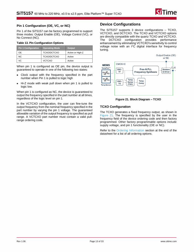
The SiT5157 supports 3 device configurations – TCXO, VCTCXO, and DCTCXO. The TCXO and VCTCXO options are directly compatible with the quartz TCXO and VCTCXO. The DCTCXO configuration provides performance enhancement by eliminating VCTCXO’s sensitivity to control voltage noise with an I2C digital interface for frequency tuning.
Figure 21. Block Diagram – TCXO
TCXO Configuration
The TCXO generates a fixed frequency output, as shown in Figure 21. The frequency is specified by the user in the frequency field of the device ordering code and then factory programmed. Other factory programmable options include supply voltage, and pin 1 functionality (OE or NC).
Refer to the Ordering Information section at the end of the datasheet for a list of all ordering options.
SiT5157 60 MHz to 220 MHz, ±0.5 to ±2.5 ppm, Elite Platform™ Super-TCXO
Rev 1.06 Page 14 of 33 www.sitime.com
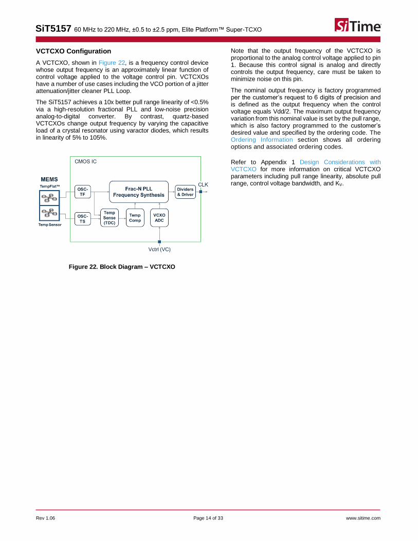
VCTCXO Configuration
A VCTCXO, shown in Figure 22, is a frequency control device whose output frequency is an approximately linear function of control voltage applied to the voltage control pin. VCTCXOs have a number of use cases including the VCO portion of a jitter attenuation/jitter cleaner PLL Loop.
The SiT5157 achieves a 10x better pull range linearity of <0.5% via a high-resolution fractional PLL and low-noise precision analog-to-digital converter. By contrast, quartz-based VCTCXOs change output frequency by varying the capacitive load of a crystal resonator using varactor diodes, which results in linearity of 5% to 105%.
Figure 22. Block Diagram – VCTCXO
Note that the output frequency of the VCTCXO is proportional to the analog control voltage applied to pin 1. Because this control signal is analog and directly controls the output frequency, care must be taken to minimize noise on this pin.
The nominal output frequency is factory programmed per the customer’s request to 6 digits of precision and is defined as the output frequency when the control voltage equals Vdd/2. The maximum output frequency variation from this nominal value is set by the pull range, which is also factory programmed to the customer’s desired value and specified by the ordering code. The Ordering Information section shows all ordering options and associated ordering codes.
Refer to Appendix 1 Design Considerations with VCTCXO for more information on critical VCTCXO parameters including pull range linearity, absolute pull range, control voltage bandwidth, and KV.

SiT5157 60 MHz to 220 MHz, ±0.5 to ±2.5 ppm, Elite Platform™ Super-TCXO
Rev 1.06 Page 15 of 33 www.sitime.com
DCTCXO Configuration
The SiT5157 offers digital control of the output frequency, as shown in Figure 23. The output frequency is controlled by writing frequency control words over the I2C interface.
There are several advantages of DCTCXOs relative to VCTCXOs:
Figure 23. Block Diagram

SiT5157 60 MHz to 220 MHz, ±0.5 to ±2.5 ppm, Elite Platform™ Super-TCXO
Rev 1.06 Page 16 of 33 www.sitime.com
VCTCXO-Specific Design Considerations
Linearity
In any VCTCXO, there will be some deviation of the frequency-voltage (FV) characteristic from an ideal straight line. Linearity is the ratio of this maximum deviation to the total pull range, expressed as a percentage. Figure 24 below shows the typical pull linearity of a SiTime VCTCXO. The linearity is excellent (1% maximum) relative to most quartz offerings because the frequency pulling is achieved with a PLL rather than varactor diodes.
Input Voltage Range
FR
EQ
EU
NC
Y
INPUT VOLTAGE
Best Straight
Line Fit
TO
TA
L P
UL
L R
AN
GE
Figure 24. Typical SiTime VCTCXO Linearity
Control Voltage Bandwidth
Control voltage bandwidth, sometimes called “modulation rate” or “modulation bandwidth”, indicates how fast a VCO can respond to voltage changes at its input. The ratio of the output frequency variation to the input voltage variation, previously denoted by KV, has a low-pass characteristic in most VCTCXOs. The control voltage bandwidth equals the modulating frequency where the output frequency deviation equals 0.707 (e.g. -3 dB) of its DC value, for DC inputs swept in the same voltage range.
For example, a part with a ±6.25 ppm pull range and a 0-3V control voltage can be regarded as having an average KV of 4.17 ppm/V (12.5 ppm/3 V = 4.17 ppm/V). Applying an input of 1.5 V DC ± 0.5 V (1.0 V to 2.0 V) causes an output frequency change of 4.17 ppm (±2.08 ppm). If the control voltage bandwidth is specified as 10 kHz, the peak-to-peak value of the output frequency change will be reduced to 4.33 ppm/√2 or 2.95 ppm, as the frequency of the control voltage change is increased to 10 kHz.
FV Characteristic Slope KV
The slope of the FV characteristic is a critical design parameter in many low bandwidth PLL applications. The slope is the derivative of the FV characteristic – the deviation of frequency divided by the control voltage change needed to produce that frequency deviation, over a small voltage span, as shown below:
in
outV
V
fK
=
It is typically expressed in kHz/Volt, MHz/Volt, ppm/Volt, or similar units. This slope is usually called “KV” based on terminology used in PLL designs.
The extreme linear characteristic of the SiTime SiT5157 VCTCXO family means that there is very little KV variation across the whole input voltage range (typically <1%), significantly reducing the design burden on the PLL designer. Figure 25 below illustrates the typical KV variation.
Input Voltage Range
KV
INPUT VOLTAGE
KV varies <1% over input
voltage range
Average
Kv
Figure 25. Typical SiTime KV Variation
SiT5157 60 MHz to 220 MHz, ±0.5 to ±2.5 ppm, Elite Platform™ Super-TCXO
Rev 1.06 Page 17 of 33 www.sitime.com
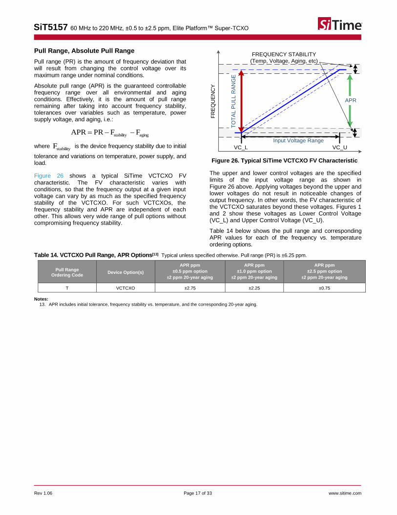
Pull Range, Absolute Pull Range
Pull range (PR) is the amount of frequency deviation that will result from changing the control voltage over its maximum range under nominal conditions.
Absolute pull range (APR) is the guaranteed controllable frequency range over all environmental and aging conditions. Effectively, it is the amount of pull range remaining after taking into account frequency stability, tolerances over variables such as temperature, power supply voltage, and aging, i.e.:
agingstability FFPRAPR −−=
where stabilityF is the device frequency stability due to initial
tolerance and variations on temperature, power supply, and load.
Figure 26 shows a typical SiTime VCTCXO FV characteristic. The FV characteristic varies with conditions, so that the frequency output at a given input voltage can vary by as much as the specified frequency stability of the VCTCXO. For such VCTCXOs, the frequency stability and APR are independent of each other. This allows very wide range of pull options without compromising frequency stability.
Input Voltage Range
FREQUENCY STABILITY
(Temp, Voltage, Aging, etc)
TO
TA
L P
UL
L R
AN
GE
FR
EQ
UE
NC
Y
APR
VC_UVC_L
Figure 26. Typical SiTime VCTCXO FV Characteristic
The upper and lower control voltages are the specified limits of the input voltage range as shown in
Figure 26 above. Applying voltages beyond the upper and lower voltages do not result in noticeable changes of output frequency. In other words, the FV characteristic of the VCTCXO saturates beyond these voltages. Figures 1 and 2 show these voltages as Lower Control Voltage (VC_L) and Upper Control Voltage (VC_U).
Table 14 below shows the pull range and corresponding APR values for each of the frequency vs. temperature ordering options.
Table 14. VCTCXO Pull Range, APR Options[13] Typical unless specified otherwise. Pull range (PR) is ±6.25 ppm.
Pull Range
Ordering Code Device Option(s)
APR ppm
±0.5 ppm option
±2 ppm 20-year aging
APR ppm
±1.0 ppm option
±2 ppm 20-year aging
APR ppm
±2.5 ppm option
±2 ppm 20-year aging
T VCTCXO ±2.75 ±2.25 ±0.75
Notes: 13. APR includes initial tolerance, frequency stability vs. temperature, and the corresponding 20-year aging.

SiT5157 60 MHz to 220 MHz, ±0.5 to ±2.5 ppm, Elite Platform™ Super-TCXO
Rev 1.06 Page 18 of 33 www.sitime.com
DCTCXO-Specific Design Considerations
Pull Range and Absolute Pull Range
Pull range and absolute pull range are described in the previous section. Table 15 below shows the pull range and corresponding APR values for each of the frequency vs. temperature ordering options.
Table 15. APR Options[14]
Pull Range Ordering Code
Pull Range ppm
APR ppm
±0.5 ppm option
±2 ppm 20-year aging
APR ppm
±1.0 ppm option
±2 ppm 20-year aging
APR ppm
±2. 5 ppm option
±2 ppm 20-year aging
T ±6.25 ±2.75 ±2.25 ±0.75
R ±10 ±6.50 ±6.0 ±4.5
Q ±12.5 ±9.0 ±8.5 ±7.0
M ±25 ±21.5 ±21.0 ±19.5
B ±50 ±46.5 ±46.0 ±44.5
C ±80 ±76.5 ±76.0 ±74.5
E ±100 ±96.5 ±96.0 ±94.5
F ±125 ±121.5 ±121.0 ±119.5
G ±150 ±146.5 ±146.0 ±144.5
H ±200 ±196.5 ±196.0 ±194.5
X ±400 ±396.5 ±396.0 ±394.5
L ±600 ±596.5 ±596.0 ±594.5
Y ±800 ±796.5 ±796.0 ±794.5
S ±1200 ±1196.5 ±1196.0 ±1194.5
Z ±1600 ±1596.5 ±1596.0 ±1594.5
U ±3200 ±3196.5 ±3196.0 ±3194.5
Notes: 14. APR includes initial tolerance, frequency stability vs. temperature, and the corresponding 20-year aging.

SiT5157 60 MHz to 220 MHz, ±0.5 to ±2.5 ppm, Elite Platform™ Super-TCXO
Rev 1.06 Page 19 of 33 www.sitime.com
Output Frequency
The device powers up at the nominal operating frequency and pull range specified by the ordering code. After power-up both pull range and output frequency can be controlled via I2C writes to the respective control registers. The maximum output frequency change is constrained by the pull range limits.
The pull range is specified by the value loaded in the digital pull-range control register. The 16 pull range choices are specified in the control register and range from ±6.25 ppm to ±3200 ppm.
Table 16 below shows the frequency resolution versus pull range programmed value
Table 16. Frequency Resolution versus Pull Range
Programmed Pull Range Frequency Resolution
±6.25 ppm 5x10-12
±10 ppm 5x10-12
±12.5 ppm 5x10-12
±25 ppm 5x10-12
±50 ppm 5x10-12
±80 ppm 5x10-12
±100 ppm 5x10-12
±120 ppm 5x10-12
±150 ppm 5x10-12
±200 ppm 5x10-12
±400 ppm 1x10-11
±600 ppm 1.4x10⁻¹¹
±800 ppm 2.1x10⁻¹¹
±1200 ppm 3.2x10⁻¹¹
±1600 ppm 4.7x10⁻¹¹
±3200 ppm 9.4x10⁻¹¹
The ppm frequency offset is specified by the 26 bit DCXO frequency control register in two’s complement format as described in the I2C Register Descriptions. The power up default value is 00000000000000000000000000b which sets the output frequency at its nominal value (0 ppm). To change the output frequency, a frequency control word is written to 0x00[15:0] (Least Significant Word) and 0x01[9:0] (Most Significant Word). The LSW value should be written first followed by the MSW value; the frequency change is initiated after the MSW value is written.
SiT5157 60 MHz to 220 MHz, ±0.5 to ±2.5 ppm, Elite Platform™ Super-TCXO
Rev 1.06 Page 20 of 33 www.sitime.com
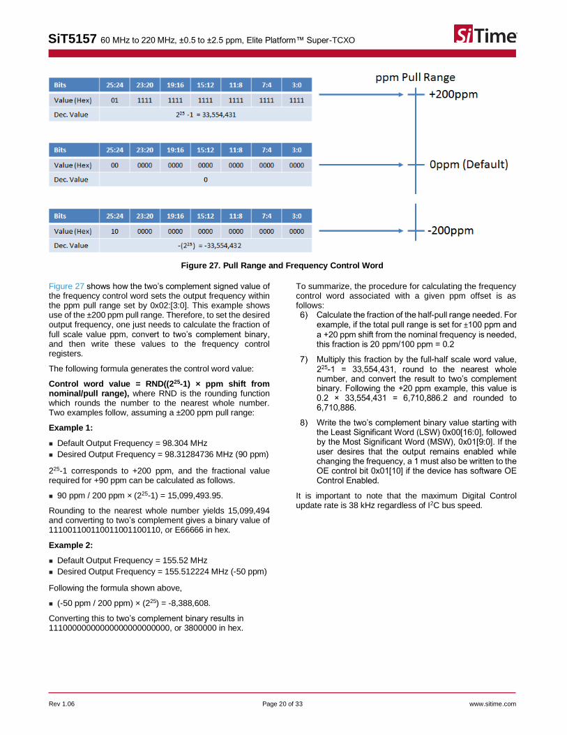
Figure 27. Pull Range and Frequency Control Word
Figure 27 shows how the two’s complement signed value of the frequency control word sets the output frequency within the ppm pull range set by 0x02:[3:0]. This example shows use of the ±200 ppm pull range. Therefore, to set the desired output frequency, one just needs to calculate the fraction of full scale value ppm, convert to two’s complement binary, and then write these values to the frequency control registers.
The following formula generates the control word value:
Control word value = RND((225-1) × ppm shift from nominal/pull range), where RND is the rounding function which rounds the number to the nearest whole number. Two examples follow, assuming a ±200 ppm pull range:
Example 1:
◼ Default Output Frequency = 98.304 MHz
◼ Desired Output Frequency = 98.31284736 MHz (90 ppm)
225-1 corresponds to +200 ppm, and the fractional value required for +90 ppm can be calculated as follows.
◼ 90 ppm / 200 ppm × (225-1) = 15,099,493.95.
Rounding to the nearest whole number yields 15,099,494 and converting to two’s complement gives a binary value of 111001100110011001100110, or E66666 in hex.
Example 2:
◼ Default Output Frequency = 155.52 MHz
◼ Desired Output Frequency = 155.512224 MHz (-50 ppm)
Following the formula shown above,
◼ (-50 ppm / 200 ppm) × (225) = -8,388,608.
Converting this to two’s complement binary results in 11100000000000000000000000, or 3800000 in hex.
To summarize, the procedure for calculating the frequency control word associated with a given ppm offset is as follows:
It is important to note that the maximum Digital Control update rate is 38 kHz regardless of I2C bus speed.
SiT5157 60 MHz to 220 MHz, ±0.5 to ±2.5 ppm, Elite Platform™ Super-TCXO
Rev 1.06 Page 21 of 33 www.sitime.com
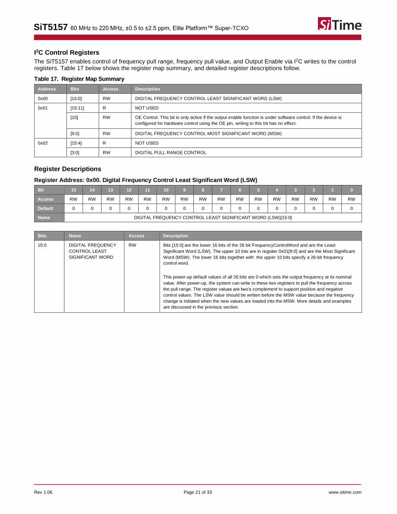
I2C Control Registers
The SiT5157 enables control of frequency pull range, frequency pull value, and Output Enable via I2C writes to the control registers. Table 17 below shows the register map summary, and detailed register descriptions follow.
Table 17. Register Map Summary
Address Bits Access Description
0x00 [15:0] RW DIGITAL FREQUENCY CONTROL LEAST SIGNIFICANT WORD (LSW)
0x01 [15:11] R NOT USED
[10] RW OE Control. This bit is only active if the output enable function is under software control. If the device is
configured for hardware control using the OE pin, writing to this bit has no effect.
[9:0] RW DIGITAL FREQUENCY CONTROL MOST SIGNIFICANT WORD (MSW)
0x02 [15:4] R NOT USED
[3:0] RW DIGITAL PULL RANGE CONTROL
Register Descriptions
Register Address: 0x00. Digital Frequency Control Least Significant Word (LSW)
Bit 15 14 13 12 11 10 9 8 7 6 5 4 3 2 1 0
Access RW RW RW RW RW RW RW RW RW RW RW RW RW RW RW RW
Default 0 0 0 0 0 0 0 0 0 0 0 0 0 0 0 0
Name DIGITAL FREQUENCY CONTROL LEAST SIGNIFICANT WORD (LSW)[15:0]
Bits Name Access Description
15:0 DIGITAL FREQUENCY
CONTROL LEAST
SIGNIFICANT WORD
RW Bits [15:0] are the lower 16 bits of the 26 bit FrequencyControlWord and are the Least
Significant Word (LSW). The upper 10 bits are in regsiter 0x01[9:0] and are the Most Significant
Word (MSW). The lower 16 bits together with the upper 10 bits specify a 26-bit frequency
control word.
This power-up default values of all 26 bits are 0 which sets the output frequency at its nominal
value. After power-up, the system can write to these two registers to pull the frequency across
the pull range. The register values are two’s complement to support positive and negative
control values. The LSW value should be written before the MSW value because the frequency
change is initiated when the new values are loaded into the MSW. More details and examples
are discussed in the previous section.
SiT5157 60 MHz to 220 MHz, ±0.5 to ±2.5 ppm, Elite Platform™ Super-TCXO
Rev 1.06 Page 22 of 33 www.sitime.com
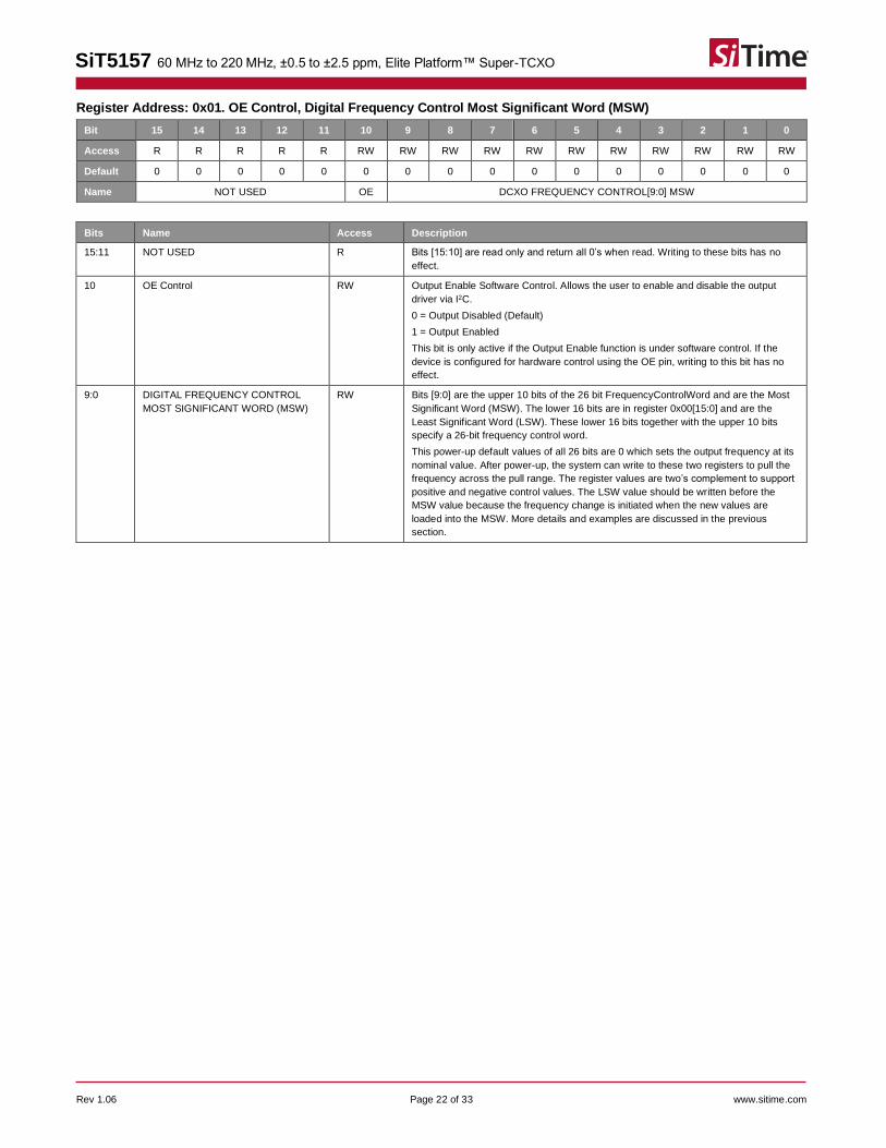
Register Address: 0x01. OE Control, Digital Frequency Control Most Significant Word (MSW)
Bit 15 14 13 12 11 10 9 8 7 6 5 4 3 2 1 0
Access R R R R R RW RW RW RW RW RW RW RW RW RW RW
Default 0 0 0 0 0 0 0 0 0 0 0 0 0 0 0 0
Name NOT USED OE DCXO FREQUENCY CONTROL[9:0] MSW
Bits Name Access Description
15:11 NOT USED R Bits [15:10] are read only and return all 0’s when read. Writing to these bits has no
effect.
10 OE Control RW Output Enable Software Control. Allows the user to enable and disable the output
driver via I2C.
0 = Output Disabled (Default)
1 = Output Enabled
This bit is only active if the Output Enable function is under software control. If the
device is configured for hardware control using the OE pin, writing to this bit has no
effect.
9:0 DIGITAL FREQUENCY CONTROL
MOST SIGNIFICANT WORD (MSW)
RW Bits [9:0] are the upper 10 bits of the 26 bit FrequencyControlWord and are the Most
Significant Word (MSW). The lower 16 bits are in register 0x00[15:0] and are the
Least Significant Word (LSW). These lower 16 bits together with the upper 10 bits
specify a 26-bit frequency control word.
This power-up default values of all 26 bits are 0 which sets the output frequency at its
nominal value. After power-up, the system can write to these two registers to pull the
frequency across the pull range. The register values are two’s complement to support
positive and negative control values. The LSW value should be written before the
MSW value because the frequency change is initiated when the new values are
loaded into the MSW. More details and examples are discussed in the previous
section.

SiT5157 60 MHz to 220 MHz, ±0.5 to ±2.5 ppm, Elite Platform™ Super-TCXO
Rev 1.06 Page 23 of 33 www.sitime.com
Register Address: 0x02. DIGITAL PULL RANGE CONTROL[15]
Bit 15 14 13 12 11 10 9 8 7 6 5 4 3 2 1 0
Access R R R R R R R R R R R R RW RW RW RW
Default 0 0 0 0 0 0 0 0 0 0 0 0 X X X X
Name NONE DIGITAL PULL RANGE CONTROL
Notes: 15. Default values are factory set but can be over-written after power-up.
Bits Name Access Description
15:4 NONE R Bits [15:4] are read only and return all 0’s when read. Writing to these bits has no
effect.
3:0 DIGITAL PULL RANGE CONTROL RW Sets the digital pull range of the DCXO. The table below shows the available pull range
values and associated bit settings. The default value is factory programmed.
Bit
3 2 1 0
0 0 0 0: ±6.25 ppm
0 0 0 1: ±10 ppm
0 0 1 0: ±12.5 ppm
0 0 1 1: ±25 ppm
0 1 0 0: ±50 ppm
0 1 0 1: ±80 ppm
0 1 1 0: ±100 ppm
0 1 1 1: ±125 ppm
1 0 0 0: ±150 ppm
1 0 0 1: ±200 ppm
1 0 1 0: ±400 ppm
1 0 1 1: ±600 ppm
1 1 0 0: ±800 ppm
1 1 0 1: ±1200 ppm
1 1 1 0: ±1600 ppm
1 1 1 1: ±3200 ppm

SiT5157 60 MHz to 220 MHz, ±0.5 to ±2.5 ppm, Elite Platform™ Super-TCXO
Rev 1.06 Page 24 of 33 www.sitime.com
Serial Interface Configuration Description
The SiT5157 includes an I2C interface to access registers that control the DCTCXO frequency pull range, and frequency pull value. The SiT5157 I2C slave-only interface supports clock speeds up to 1 Mbit/s. The SiT5157 I2C module is based on the I2C specification, UM1024 (Rev.6 April 4, 2014 of NXP Semiconductor).
Serial Signal Format
The SDA line must be stable during the high period of the SCL. SDA transitions are allowed only during SCL low level for data communication. Only one transition is allowed during the low SCL state to communicate one bit of data. Figure 28 shows the detailed timing diagram.
An idle I2C bus state occurs when both SCL and SDA are not being driven by any master and are therefore in a logic HI state due to the pull up resistors. Every transaction begins with a START (S) signal and ends with a STOP (P) signal. A START condition is defined by a high to low transition on the SDA while SCL is high. A STOP condition is defined by a low to high transition on the SDA while SCL is high. START and STOP conditions are always generated by the master. This slave module also supports repeated START (Sr) condition which is same as START condition instead of STOP condition (the blue-color line shows repeated START in Figure 29).
SDA
SCL
data line stable:
data valid
change of data
allowed
setup time
Figure 28. Data and clock timing relation in I2C bus
SDA
SCL
S P
START Condition STOP Condition
hold time setup timehold time
Figure 29. START and STOP (or repeated START, blue line) condition
SiT5157 60 MHz to 220 MHz, ±0.5 to ±2.5 ppm, Elite Platform™ Super-TCXO
Rev 1.06 Page 25 of 33 www.sitime.com
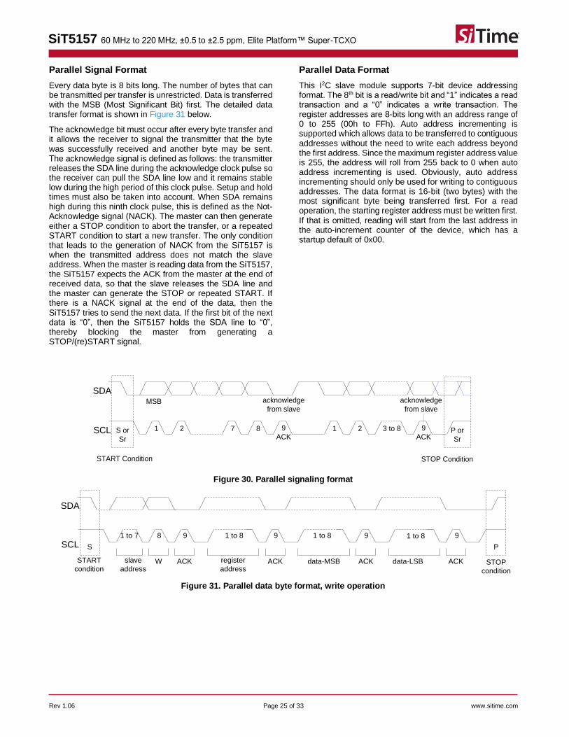
Parallel Signal Format
Every data byte is 8 bits long. The number of bytes that can be transmitted per transfer is unrestricted. Data is transferred with the MSB (Most Significant Bit) first. The detailed data transfer format is shown in Figure 31 below.
The acknowledge bit must occur after every byte transfer and it allows the receiver to signal the transmitter that the byte was successfully received and another byte may be sent. The acknowledge signal is defined as follows: the transmitter releases the SDA line during the acknowledge clock pulse so the receiver can pull the SDA line low and it remains stable low during the high period of this clock pulse. Setup and hold times must also be taken into account. When SDA remains high during this ninth clock pulse, this is defined as the Not-Acknowledge signal (NACK). The master can then generate either a STOP condition to abort the transfer, or a repeated START condition to start a new transfer. The only condition that leads to the generation of NACK from the SiT5157 is when the transmitted address does not match the slave address. When the master is reading data from the SiT5157, the SiT5157 expects the ACK from the master at the end of received data, so that the slave releases the SDA line and the master can generate the STOP or repeated START. If there is a NACK signal at the end of the data, then the SiT5157 tries to send the next data. If the first bit of the next data is “0”, then the SiT5157 holds the SDA line to “0”, thereby blocking the master from generating a STOP/(re)START signal.
Parallel Data Format
This I2C slave module supports 7-bit device addressing format. The 8th bit is a read/write bit and “1” indicates a read transaction and a “0” indicates a write transaction. The register addresses are 8-bits long with an address range of 0 to 255 (00h to FFh). Auto address incrementing is supported which allows data to be transferred to contiguous addresses without the need to write each address beyond the first address. Since the maximum register address value is 255, the address will roll from 255 back to 0 when auto address incrementing is used. Obviously, auto address incrementing should only be used for writing to contiguous addresses. The data format is 16-bit (two bytes) with the most significant byte being transferred first. For a read operation, the starting register address must be written first. If that is omitted, reading will start from the last address in the auto-increment counter of the device, which has a startup default of 0x00.
SDA
SCL S or
Sr
P or
Sr
START Condition STOP Condition
MSB
1 2 7 8 9
ACK1 2 3 to 8
acknowledge
from slave
9
ACK
acknowledge
from slave
Figure 30. Parallel signaling format
SDA
SCL S P
START
conditionSTOP
condition
8 91 to 7 91 to 8 91 to 8
slave
addressW ACK ACK ACKdata-MSBregister
address
91 to 8
ACKdata-LSB
Figure 31. Parallel data byte format, write operation

SiT5157 60 MHz to 220 MHz, ±0.5 to ±2.5 ppm, Elite Platform™ Super-TCXO
Rev 1.06 Page 26 of 33 www.sitime.com
SDA
SCL S P
START
conditionSTOP
condition
8 91 to 7 91 to 8
slave
addressR ACK ACKdata-MSB
91 to 8
ACKdata-LSB
Figure 32. Parallel data byte format, read operation
Figure 33 below shows the I2C sequence for writing the 4-byte control word using auto address incrementing.
STOP
condition
OutputFrequency
f0
Tfdelay
Tsettle
f0 + f1 ±0.5%
St D_Address[6:0] W A R_Address[7:0]=00 A
0x00[15:8]
A
0x00[7:0]
A
Digital Frequency Control – Least Significant Word (LSW) [15:0]
X X X X X OE
0x01[15:8]
A MSW[7:0] A Sp
Digital Frequency Control – Most Significant Word (MSW) [9:0]
LSW[15:8] LSW[7:0]
0x01[7:0]
9 8
Slave Drives Bit(s) on Bus
Master Drives Bit(s) on Bus
St Start
Sp Stop
W Write
R Read
A Acknowledge
OE Output Enable
X “Don’t Care” Register Bit not used.
Figure 33. Writing the Frequency Control Word
Table 18. DCTCXO Delay and Settling Time
Parameter Symbol Minimum Typical Maximum Units Notes
Frequency Change Delay Tfdelay – 103 140 µs Time from end of 0x01 reg MSW to start of frequency pull, as shown in Figure 33
Frequency Settling Time Tsettle – 16.5 20 µs Time to settle to 0.5% of frequency offset, as shown in Figure 33

SiT5157 60 MHz to 220 MHz, ±0.5 to ±2.5 ppm, Elite Platform™ Super-TCXO
Rev 1.06 Page 27 of 33 www.sitime.com
I2C Timing Specification
The below timing diagram and table illustrate the timing relationships for both master and slave.
Figure 34. I2C Timing Diagram
Table 19. I2C Timing Requirements
Parameter Speed Mode Value Unit
tSETUP FM+ (1 MHz) > 50 nsec
FM (400 KHz) > 100 nsec
SM (100 KHz) > 250 nsec
tHOLD FM+ (1 MHz) > 0 nsec
FM (400 KHz) > 0 nsec
SM (100 KHz) > 0 nsec
tVD:AWK FM+ > 450 nsec
FM (400 KHz) > 900 nsec
SM (100 KHz) > 3450 nsec
tVD:DAT NA (s-awk + s-data)/(m-awk/s-data)
master spec both (slave/master) spec

SiT5157 60 MHz to 220 MHz, ±0.5 to ±2.5 ppm, Elite Platform™ Super-TCXO
Rev 1.06 Page 28 of 33 www.sitime.com
I2C Device Address Modes
There are two I2C address modes:
Table 20. Factory Programmed I2C Address Control [16]
I2C Address Ordering Code Device I2C Address
0 1100000
1 1100001
2 1100010
3 1100011
4 1100100
5 1100101
6 1100110
7 1100111
8 1101000
9 1101001
A 1101010
B 1101011
C 1101100
D 1101101
E 1101110
F 1101111
Notes: 16. Table 20 is only valid for the DCTCXO device option which supports
I2C Control.
Table 21. Pin Selectable I2C Address Control [17]
A0
Pin 5 I2C Address
0 1100010
1 1101010
Notes: 17. Table 21 is only valid for the DCTCXO device option which supports
I2C control and A0 Device Address Control Pin.

SiT5157 60 MHz to 220 MHz, ±0.5 to ±2.5 ppm, Elite Platform™ Super-TCXO
Rev 1.06 Page 29 of 33 www.sitime.com
Schematic Example
Figure 35. DCTCXO schematic example
SiT5157 60 MHz to 220 MHz, ±0.5 to ±2.5 ppm, Elite Platform™ Super-TCXO
Rev 1.06 Page 30 of 33 www.sitime.com
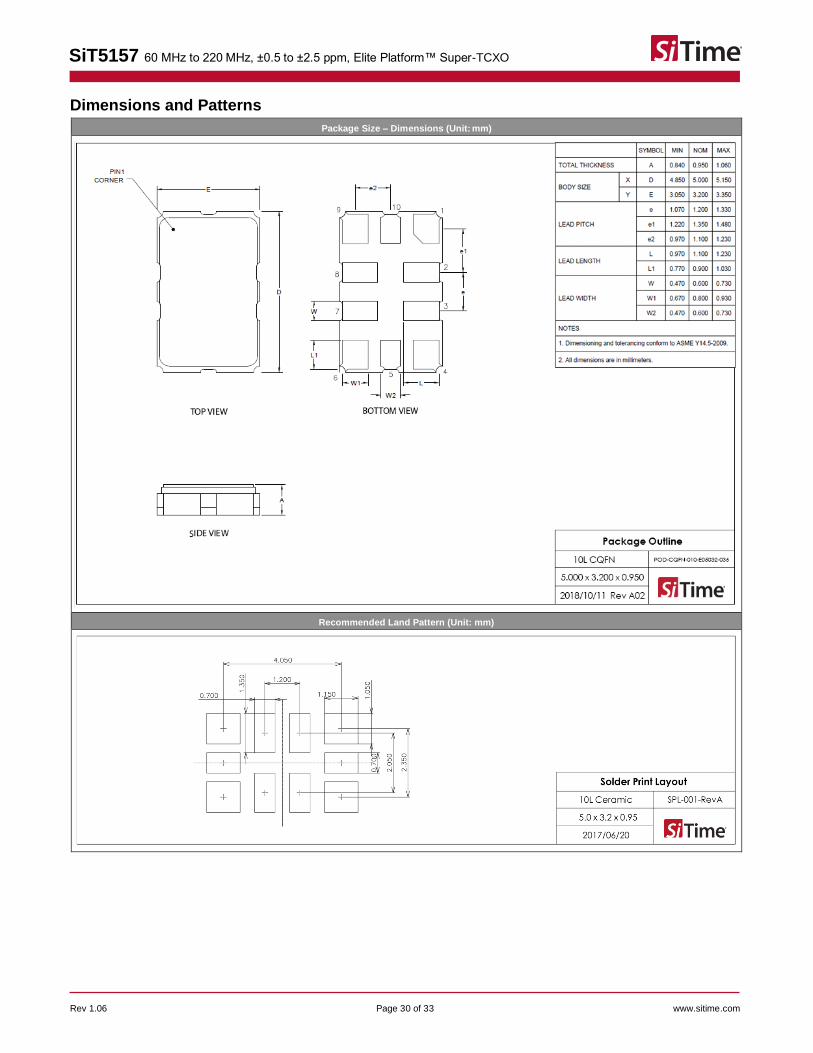
Dimensions and Patterns
Package Size – Dimensions (Unit: mm)
Recommended Land Pattern (Unit: mm)

SiT5157 60 MHz to 220 MHz, ±0.5 to ±2.5 ppm, Elite Platform™ Super-TCXO
Rev 1.06 Page 31 of 33 www.sitime.com
Layout Guidelines
◼ The SiT5157 uses internal regulators to minimize the impact of power supply noise. For further reduction of noise, it is essential to use two bypass capacitors (0.1 μF and 10 μF). Place the 0.1 uF capacitor as close to the VDD pin as possible, typically within 1 mm to 2 mm. Place the 10 uF capacitor within 2 inches of the device VDD and VSS pins.
◼ It is also recommended to connect all NC pins to the ground plane and place multiple vias under the GND pin for maximum heat dissipation.
◼ For additional layout recommendations, refer to the Best Design Layout Practices.
Manufacturing Guidelines
The SiT5157 Super-TCXOs are precision timing devices. Proper PCB solder and cleaning processes must be followed to ensure best performance and long-term reliability.
◼ No Ultrasonic or Megasonic Cleaning: Do not subject the SiT5157 to an ultrasonic or megasonic cleaning environment. Otherwise, permanent damage or long-term reliability issues to the device may result.
◼ No external cover. Unlike legacy quartz TCXOs, the SiT5157 is engineered to operate reliably, without performance degradation in the presence of ambient disturbers such as airflow and sudden temperature changes. Therefore, the use of an external cover typically required by quartz TCXOs is not needed.
◼ Reflow profile: For mounting these devices to the PCB, IPC/JEDEC J-STD-020 compliant reflow profile must be used. Device performance is not guaranteed if soldered manually or with a non-compliant reflow profile.
◼ PCB cleaning: After the surface mount (SMT)/reflow process, solder flux residues may be present on the PCB and around the pads of the device. Excess residual solder flux may lead to problems such as pad corrosion, elevated leakage currents, increased frequency aging, or other performance degradation. For optimal device performance and long-term reliability, thorough cleaning to remove all the residual flux and drying of the PCB is required as shortly after the reflow process as possible. Water soluble flux is recommended. In addition, it is highly recommended to avoid the use of any “no clean” flux. However, if the reflow process necessitates the use of “no clean” flux, then utmost care should be taken to remove all residual flux between SiTime device and the PCB. Note that ultrasonic PCB cleaning should not be used with SiTime oscillators.
◼ For additional manufacturing guidelines and marking/ tape-reel instructions, refer to SiTime Manufacturing Notes.
SiT5157 60 MHz to 220 MHz, ±0.5 to ±2.5 ppm, Elite Platform™ Super-TCXO
Rev 1.06 Page 32 of 33 www.sitime.com
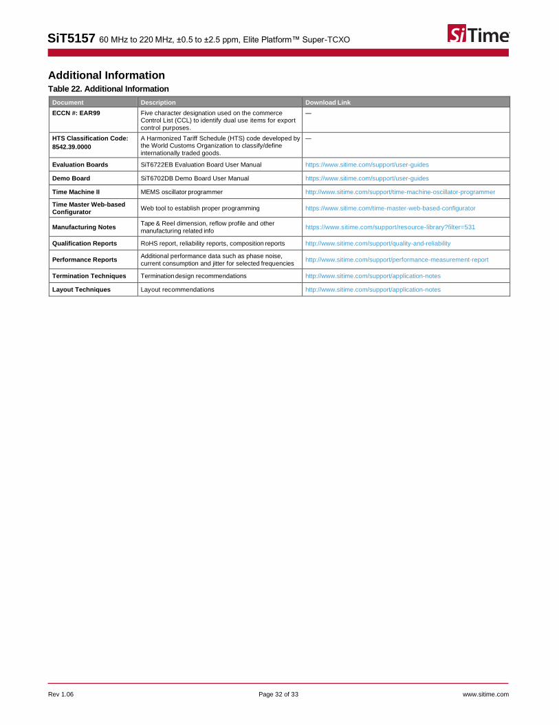
Additional Information Table 22. Additional Information
Document Description Download Link
ECCN #: EAR99 Five character designation used on the commerce Control List (CCL) to identify dual use items for export control purposes.
—
HTS Classification Code:
8542.39.0000
A Harmonized Tariff Schedule (HTS) code developed by the World Customs Organization to classify/define internationally traded goods.
—
Evaluation Boards SiT6722EB Evaluation Board User Manual https://www.sitime.com/support/user-guides
Demo Board SiT6702DB Demo Board User Manual https://www.sitime.com/support/user-guides
Time Machine II MEMS oscillator programmer http://www.sitime.com/support/time-machine-oscillator-programmer
Time Master Web-based Configurator
Web tool to establish proper programming https://www.sitime.com/time-master-web-based-configurator
Manufacturing Notes Tape & Reel dimension, reflow profile and other manufacturing related info
https://www.sitime.com/support/resource-library?filter=531
Qualification Reports RoHS report, reliability reports, composition reports http://www.sitime.com/support/quality-and-reliability
Performance Reports Additional performance data such as phase noise, current consumption and jitter for selected frequencies
http://www.sitime.com/support/performance-measurement-report
Termination Techniques Termination design recommendations http://www.sitime.com/support/application-notes
Layout Techniques Layout recommendations http://www.sitime.com/support/application-notes

SiT5157 60 MHz to 220 MHz, ±0.5 to ±2.5 ppm, Elite Platform™ Super-TCXO
Rev 1.06 Page 33 of 33 www.sitime.com
Revision History Table 23. Revision History
Version Release Date Change Summary
0.1 05/10/2016 First release, advanced information
0.15 08/04/2016 Replaced QFN package with SOIC-8 package Added 10 µF bypass cap requirement Updated test circuits to reflect both new bypass cap requirement and SOIC-8 package Update Table 1 (Electrical Characteristics)
0.16 09/12/2016 Updated test circuit diagrams
0.2 09/21/2016 Revised Table 1 (Electrical Characteristics)
0.51 08/20/2017 Changed to preliminary Added DCTCXO mode Added I2C information Added 5.0 mm x 3.2 mm package information Updated test circuits Updated Table 1 (Electrical Characteristics) Updated part ordering info Misc. corrections
0.52 11/27/2017 Updated the Thermal Characteristics table
Added more on Manufacturing Guideline section
0.55 02/05/2018 Added View labels to Package Drawings Updated links and notes
0.60 03/01/2018 Added 105°C support, updated Ordering Information
1.0 07/02/2018 Updated Electrical Characteristics tables. Added Typical Performance Plots.
Improved readability. Fixed bad hyperlinks.
1.01 07/06/2018 Updated Mechanical Shock Resistance, Table 9 (Environmental Compliance).
1.02 08/02/2018 Various formatting updates.
Revised phase noise specifications.
Updated package outline drawing.
Updated conditions for one day and one year aging specs.
1.03 12/04/2018 Formatting updates Fixed APR typo for 125 ppm pull range and 0.5 ppm stability, Table 15 Corrected typos in package drawing dimensions Added nominal value for LVCMOS output impedance Increased Mechanical Shock Resistance to 30000g Added “X” order code for 250u Tape and Reel Improved I2C bus frequency specification Updated Manufacturing Guidelines to recommend water soluble flux
1.04 03/28/2020
Corrected typos for write/read I2C polarity Clarified PCB cleaning instructions Added link to SiT6702DB Added ECCN and HTS codes Modified supply and load sensitivities Formatting changes
Added note for Theta Ja Updated DCTCXO Delay and Settling Time table Removed frequency support from 200 to 208 MHz Added max and min input voltage to Absolute Maximum Limits table Updated output impedance typical spec
Clarified Initial Tolerance specification condition
Relabeled “First Pulse Accuracy” parameter to “Time to Rated Frequency Stability” for clarity
1.05 05/29/2020 Revised Parallel Data Format section description and figures
1.06 11/04/2021 Resolved a typographical error in the frequency range listing in the ordering code