features product summary - infineon technologies
TRANSCRIPT

AUIRB24427S
www.irf.com © 2014 International Rectifier Sept 29nd
, 2014
1
Features
Very low output resistance
Extended supply voltage range: 12.5V to 24V
TTL/CMOS compatible inputs
CMOS Schmitt-triggered inputs
Matched propagation delay for both channels
Outputs in phase with inputs
Enable function
Under Voltage Lock Out function
Automotive Qualified
Leadfree, RoHS compliant
Typical Applications
Automotive General Purpose Dual
Low Side Driver
Gate transformer driver
Bridge Tied Gate Transformer Driver
DC-DC converters secondary side driver
Hybrid Power Train Driver
Product Summary
Topology Dual Low Side Driver
VOUT 12.5 V – 24 V
Io+ & I o- (VCC=15V) > 6 A
Output Resistance (max)
0.65 Ohm
tON & tOFF (max) 55ns
Package
PSOIC-8N
Typical Connection Diagram
VCC
INA
COM
INB
OUTA
OUTB
TO
LOAD
ENRg
Rg
NC
-Vbatt
+
Logic level
input
Orderable Part Number Package Type
Standard Pack Note
Form Quantity
AUIRB24427STR PSOIC8-N Tape & Reel 2500

AUIRB24427S
www.irf.com © 2014 International Rectifier Sept 29nd
, 2014
2
Absolute Maximum Ratings Absolute Maximum Ratings indicate sustained limits beyond which damage to the device may occur. All voltage parameters are absolute voltages referenced to COM lead. Stresses beyond those listed under " Absolute Maximum Ratings" may cause permanent damage to the device. These are stress ratings only; and functional operation of the device at these or any other condition beyond those indicated in the ―Recommended Operating Conditions‖ is not implied. Exposure to absolute-maximum-rated conditions for extended periods may affect device reliability. The thermal resistance and power dissipation ratings are measured under board mounted and still air conditions. Ambient temperature (TA) is 25°C, unless otherwise specified.
Recommended Operating Conditions
For proper operation the device should be used within the recommended conditions. All voltage parameters are absolute voltage referenced to COM.
Symbol Definition Min. Max. Units
Vcc Fixed supply voltage -0.3 24
V VO Output voltage -0.3 24
VIN Logic input voltage -0.3 5.5
VEN Logic enable voltage -0.3 5.5
RthJc Thermal resistance, junction to case — 4 °C/W
TJ Junction temperature — 150
°C TS Storage temperature -55 150
TL Lead temperature (soldering, 10 seconds) — 300
Symbol Definition Min. Max. Units
Vcc Fixed supply voltage 5 20
V VO Output voltage 0 VCC
VIN Logic input voltage 0 5
VEN Logic enable voltage 0 5
TA Ambient temperature -40 125 °C
Rg External gate resistance 2.5
CBP VCC to COM bypass capacitance – X7R dielectric type.
1 F

AUIRB24427S
www.irf.com © 2014 International Rectifier Sept 29nd
, 2014
3
Static Electrical Characteristics
Unless otherwise specified, these specifications apply for an operating junction temperature range of -40°C≤Ta≤125°C and power supply VCC=15 V. The VIN and IIN parameters are referenced to COM and are applicable to input leads: INA and INB. The VO and IO parameters are referenced to COM and are applicable to the output leads: OUTA and OUTB.
(†) Guaranteed by design
Symbol Definition Min Typ Max Units Test Conditions
VIL Logic ―0‖ input voltage 0.8
V
VIH Logic ―1‖ input voltage 2.5
VHYS-IN Input voltage hysteresis 0.8
VENL Logic ―0‖ enable voltage 0.8
VENH Logic ―1‖ enable voltage 2.5
VHYS-EN Enable voltage hysteresis 0.8
ROH+25 Source Output resistance 450
m
Ta=+25C ROL+25 Sink Output resistance 450
ROH+125 Source Output resistance 650 Ta=+125C
ROL+125 Sink Output resistance 650
VOH+25 Output high level voltage Vcc-Vo 450
mV
Ta=+25C, Iout=100mA VOL+25 Output low level voltage Vo 450
VOH+125 Output high level voltage Vcc-Vo 650 Ta=+125C, Iout=100mA
VOL+125 Output low level voltage Vo 650
IIN+ Logic ―1‖ input bias current 25 50 µA
VIN=5V, VCC=15V
IIN- Logic ―0‖ input bias current 1 VIN=0V, VCC=15V
IQB Quiescent supply current 0.5 1.2 2.5 mA VCC=15V, INA & INB
not switching
VCCUVHYS Vcc supply undervoltage hysteresis 1.5
V
VCCUV+ Vcc supply undervoltage turn on threshold 10.5 11.5 12.6
VCCUV- Vcc supply undervoltage turn off threshold 9.0 10.0 11
IO+ Output high short circuit pulsed current(†)
6 A
VCC=15V, PW<10us
IO- Output high short circuit pulsed current(†)
6 VCC=15V, PW<10us

AUIRB24427S
www.irf.com © 2014 International Rectifier Sept 29nd
, 2014
4
Dynamic Electrical Characteristics
Unless otherwise noted, these specifications apply for an operating junction temperature range of -40°C≤Ta≤125°C with bias conditions of VCC = 15 V, CL = 4700pF. Refer to Figure T2 for switching time definition and to Figure T3 for switching time test circuit (page 15).
Input/Output table
EN INA INB OUTA OUTB
L X L L
L X L L
H L L L L
H H H H H
This table is held true in the voltages ranges defined in the recommended conditions section. See also Fig. T1 on page 14.
Symbol Definition Min Typ Max Units Test Conditions
Propagation delay characteristics
ns CBP=10uF
TON Turn-on propagation delay — 40
TOFF Turn-off propagation delay — 55
TON-EN Enable Turn-on propagation delay — 40
TOFF-EN Enable Turn-off propagation delay — 55
tr Turn-on rise time — 33
tf Turn-off fall time — 33

AUIRB24427S
www.irf.com © 2014 International Rectifier Sept 29nd
, 2014
5
Functional Block Diagram:

AUIRB24427S
www.irf.com © 2014 International Rectifier Sept 29nd
, 2014
6
Input/Output/Enable Pin Equivalent Circuit Diagrams
VCC
COM
OUTA
OUTB
ESD
Diode
ESD
Diode
24V
Lead Definitions
PIN Symbol Description
1 EN Enable pin
2 INA Logic input for gate driver output (OUTA), in phase
3 COM Ground
4 INB Logic input for gate driver output (OUTB), in phase
5 OUTB Gate drive output B
6 VCC Supply voltage
7 OUTA Gate drive output A
8 NC No connection

AUIRB24427S
www.irf.com © 2014 International Rectifier Sept 29nd
, 2014
7
Package Information

AUIRB24427S
www.irf.com © 2014 International Rectifier Sept 29nd
, 2014
8
Sym
bo
ls Dimensions
Millimiter Inches
MIN MAX MIN MAX
A --- 1.70 --- .067
A1 0 0.10 0 .004
A2 1.25 --- .049 ---
b 0.31 0.51 .012 .020
c 0.17 0.25 .007 .010
D 4.90 .193
D1 3.20 3.40 .126 .134
E 6.00 BSC .236 BSC
E1 3.90 BSC .153 BSC
E2 1.00 --- .039 ---
e 1.27 BSC .050 BSC
h 0.25 0.50 .010 .020
L 0.40 1.27 .016 .050
L1 1.04 REF .041 REF
L2 0.25 BSC .010 BSC
Θ 0 8 0 8
Recommended PCB footprint

AUIRB24427S
www.irf.com © 2014 International Rectifier Sept 29nd
, 2014
9
Part Marking Information

AUIRB24427S
www.irf.com © 2014 International Rectifier Sept 29nd
, 2014
10
Application Information
1. Gate Driver The AUIRB24427S has been designer as a high current gate driver for single ended applications.
Thanks to its very high output current and low thermal resistance vs. pcb, it is capable to drive Mosfets
with very large input capacitance at frequencies up to fsw=200kHz or higher without the need of negative
supply. The following figure 1 shows the typical device application schematic:
VCC
INA
COM
INB
OUTA
OUTB
LOAD
ENRg
Rg
NCLogic level
input
LOADVcc
Cbp
Figure 1: typical gate driver application
Rg values have to be selected based on the requested tr and tf of the application and may vary between
2.5 and 20while the input capacitance of the Fets can go up to 20nF or more depending on fsw.
Since the very high peak output current, the bypass capacitor Cpb has to be mounted in the close proximity
of the Vcc and COM pins and a ceramic type with low ESR has to be chosen.
2. BT-GTD (Bridge Tied Gate Transformer Driver)
This is a popular configuration that allows driving high side Fets using a low side gate driver, the Fig. 2
shows the typical schematic for a single Fet drive:
VCC
INA
COM
INB
OUTA
OUTB
ENRg,ps
Rg,ps
NCLogic level
input Rg,ssCdec
PulseTransf.
Vcc
Cbp
Figure 2: Bridge Tied Gate Driver configuration
In this configuration the gate transformer parameters have a very important role, most manufacturers
indicate the following in their datasheets:
V*s ratings: this factor must be respected, in bipolar drive application (like the one shown in
Fig.2) a maximum of up to twice that parameter is still acceptable for most manufacturers, this
factor then must be chosen accordingly to the following formula:

AUIRB24427S
www.irf.com © 2014 International Rectifier Sept 29nd
, 2014
11
(1)
where Vprim is the voltage applied to the primary, is the duty cycle and fsw the switching
frequency of the application;
N, turns ratio: usually 1:1, in some cases 1:2 or 1:1:1 (dual driver) this determines the voltage ratio
between primary and secondary;
Lp, primary inductance: this value determines the magnetizing inductance as follows:
(2)
where K is the coupling factor between primary and secondary windings.
LLK, leakage inductance: this parameter, usually indicated at primary, is equal to:
(3)
The higher is Lm, the lower is the magnetizing current flowing into the transformer and consequent power
losses into the driver. On the other hand the lower is LLK, the lower and shorter will be the ringing of the
secondary LC network created by LLK, and Ciss of the Fet, damped by Rg,ss and much lower overshot will
appear on the Vgs across the Fet during transition. Then a too high Lm requires a very good mechanical
construction of the gate transformer to achieve high K and consequent low LLK.
In a gate driver application running in the range of 50kHz-200kHz and using the AUIRB24427S, a good
choice is usually a Lm between 300uH and 2mH and a LLK < 1uH. This translate for the formula (2) and (3)
above in a coupling factor K between 0.9940 and 0.9995
For good operation and to reduce unneeded power losses into the AUIRB24427S driver, the magnetizing
current has to be kept ILM < 0.5A, from this then derives a minimum Lm to be calculated as follows:
(4)
Where Vg is the gate driving voltage of the Fet
Fig. 2.a show a good design waveform obtained with the following parameters:
Vg=+/-15V, Lm=400uH, LLK=0.4uH, N=1, fsw=100kHz, CissFET =10nF, Rg,ps=3, Rg,ss=4Cdec=1uF Cdec is the AC coupling capacitor needed to reset the driver transformer flux, its value has to be calculated
in a way that the voltage across it can be considered constant during normal operation. The higher the fsw
the smaller will be Cdec. A ceramic capacitor is normally used.

AUIRB24427S
www.irf.com © 2014 International Rectifier Sept 29nd
, 2014
12
Figure 3a: Bridge Tied Gate Driver waveforms
The waveforms in Fig. 2a show that:
The lower is LLK, the lower and shorter is the ringing on the Fets gate voltage, particular care must
be paid to guarantee that the max Vgs voltage of the Fet is not exceeded during operation;
The lower is LLK, the shorter is the propagation delay from the driver to the gate of the Fet and the
higher is the peak current into its gate;
The higher is Lm, the lower is ILM; at the primary side the gate peak current, summed to ILM,
constitute the total current flowing out of the gate driver.

AUIRB24427S
www.irf.com © 2014 International Rectifier Sept 29nd
, 2014
13
3. Driving circuitry design: thermal considerations The following design example shows how to get a proper design of the gate driving circuitry considering the following target application data:
Switching frequency 150kHz.
Load capacitance range [10-100] nF.
Supply voltage Vcc=12V. The switching losses due to the charge/discharge of the capacitive load CL represent the main component of the IC power dissipation. These losses are proportionally shared between the IC output resistance and the external gate resistance Rg. As a consequence the thermal behavior of the IC, with the constraint of a maximum junction temperature equal to 150°C, is one of the key points in dimensioning the system parameters. Figure 3 shows the power that is dissipated inside the IC as a function of load capacitance CL. The external resistance Rg has been chosen in order to keep the product RL*Cg as constant and equal to 300ns (refer to Figure 4 for switching circuit schematic). For a given parameter sizing the value of Pow allows to calculate the junction temperature Tj as:
JAthAJ RPowTT (1)
Where TA is the ambient temperature and RthJA is the junction to ambient thermal resistance.
Figure 3: Simulated IC power dissipation as a function of load capacitance.
IC dissipated power
0.000
0.100
0.200
0.300
0.400
0.500
0.600
0.700
0 10 20 30 40 50 60 70 80 90 100
C [nF]
Po
w [
W]

AUIRB24427S
www.irf.com © 2014 International Rectifier Sept 29nd
, 2014
14
4. Bias and Transient Conditions The input pins of the IC are protected by ESD events with the circuitry shown into ―Functional block diagram‖ section at par.: Input/Output/Enable Pin Equivalent Circuit Diagrams. This shows that an ESD diode is placed in between each of these pins and Vcc. In case Vcc voltage will be lower than one of the voltage applied to these pins the diode will conduct. Because of its power dissipation the junction temperature will increase. In order to avoid dangerous working conditions it is recommended to keep the Vcc voltage always higher or equal to the INA/INB/Enable pin voltages; it is remind that input voltage must respect the defined absolute maximum rating limits.
5. System functionality with improved thermal behavior. The PSOIC8N package is characterized by a metal thermal pad whose functionality is to reduce the junction to case thermal resistance. In order to better exploit this feature it is necessary to reduce as much as possible the thermal pad to PCB thermal resistance (RthTP-PCB in. Fig. 4). Two possible ways are suggested: a- Foresee a footprint on layout that allows to solder the thermal pad to the PCB. b- Use thermal material filling the air gap in between the thermal pad and the PCB.
PCB
Plastic Case
Thermal PadSolder
Paste
J
TPRthj-TP
RthTP-PCB
PCB
Ambient
RthPCB-a
Figure 4: Steady state equivalent thermal circuit.
6. Square input pulse distortion The following chapter provides a characterization of pulse width distortion. This is defined as the ratio between the output pulse width with respect to input pulse width. Characterization is done with no load on OUTA and OUTB and it is applicable to both INA, INB and EN input pulses. Fig. 5a and 5b show the output pulse length with respect to input pulse length. In particular, Fig. 5a describes the pulse distortion in case of a short turn-on input pulse (e.g. low duty cycle condition); while Fig. 5b shows the pulse distortion in case of a turn-off input pulse (e.g. high duty cycle condition).

AUIRB24427S
www.irf.com © 2014 International Rectifier Sept 29nd
, 2014
15
a
b
Fig. 5 Output pulse distortion in case of a short turn-on input pulse (a) and turn-off input pulse (b).
0
50
100
150
200
250
0 50 100 150 200 250
Ou
tpu
t p
uls
e w
idth
[n
s]
Input pulse width [ns]
REAL
IDEAL
0
50
100
150
200
250
0 50 100 150 200 250
Ou
tpu
t p
uls
e w
idth
[n
s]
Input pulse width [ns]
REAL
IDEAL

AUIRB24427S
www.irf.com © 2014 International Rectifier Sept 29nd
, 2014
16
7. Bypass capacitor The bypass capacitor stores an electrical charge that is released to the power line whenever a transient voltage spike occurs. It provides a low-impedance supply source and it minimizes the noise generated by the switching of the outputs. It is recommended to place the bypass capacitor as close as possible to the gate driver in order to improve its effectiveness by reducing the effect of parasitic inductance of PCB lines. The value of bypass capacitor is related to: a- the current that the gate driver has to provide to the OUTA/B loads during turn-on switching condition; b- the speed at which the output pin is driven; c- the maximum allowed drop on power supply pins.
For instance, if it considered that outputs OUTA and OUTB provide 6A source current with 20ns rise time and the maximum wished drop on VCC pin is 0.1V, then the bypass capacitance can be calculated as:
FV
nsA
V
TInC 4.2
1.0
206*2*
(1)
Where n is the number of outputs that are switching at the same time. In this case it has been considered that OUTA and OUTB are driven in phase. Equation 1 does not contain the information about capacitance ESR that introduces a further drop in the power supply voltage. As a consequence it is recommended to use low ESR capacitances (e.g. X7R dielectric material).
Additional Details
Figure T1: Input/output Timing Diagram

AUIRB24427S
www.irf.com © 2014 International Rectifier Sept 29nd
, 2014
17
Figure T2: Switching Time Waveform Definitions
VCC
INA
COM
INB
OUTA
OUTB
EN NC
Cgb Cga
-
Vbatt +CBP
VCC
GND
GND VCC
EN
IN
IN
Parameter Definitio EN IN
TON Turn-on propagation delay 5V Pulse 0V to 5V
TOFF Turn-off propagation delay 5V Pulse 5V to 0V
TON-EN Enable Turn-on propagation delay
Pulse 0V to 5V 5V
TOFF-EN Enable Turn-off propagation delay
Pulse 5V to 0V 5V
Figure T3: Switching Time Test Circuit and test conditions
AUIRB24427S
www.irf.com © 2014 International Rectifier Sept 29nd
, 2014
18
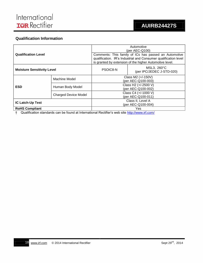
Qualification Information
Qualification Level
Automotive
(per AEC-Q100)
Comments: This family of ICs has passed an Automotive qualification. IR’s Industrial and Consumer qualification level is granted by extension of the higher Automotive level.
Moisture Sensitivity Level PSOIC8-N MSL3,
260°C
(per IPC/JEDEC J-STD-020)
ESD
Machine Model Class M2 (+/-150V)
(per AEC-Q100-003)
Human Body Model Class H2 (+/-2500 V) (per AEC-Q100-002)
Charged Device Model Class C4 (+/-1000 V) (per AEC-Q100-011)
IC Latch-Up Test Class II, Level A
(per AEC-Q100-004)
RoHS Compliant Yes
† Qualification standards can be found at International Rectifier’s web site http://www.irf.com/

AUIRB24427S
www.irf.com © 2014 International Rectifier Sept 29nd
, 2014
19
IMPORTANT NOTICE
Unless specifically designated for the automotive market, International Rectifier Corporation and its subsidiaries (IR) reserve the right to make corrections, modifications, enhancements, improvements, and other changes to its products and services at any time and to discontinue any product or services without notice. Part numbers designated with the ―AU‖ prefix follow automotive industry and / or customer specific requirements with regards to product discontinuance and process change notification. All products are sold subject to IR’s terms and conditions of sale supplied at the time of order acknowledgment. IR warrants performance of its hardware products to the specifications applicable at the time of sale in accordance with IR’s standard warranty. Testing and other quality control techniques are used to the extent IR deems necessary to support this warranty. Except where mandated by government requirements, testing of all parameters of each product is not necessarily performed. IR assumes no liability for applications assistance or customer product design. Customers are responsible for their products and applications using IR components. To minimize the risks with customer products and applications, customers should provide adequate design and operating safeguards. Reproduction of IR information in IR data books or data sheets is permissible only if reproduction is without alteration and is accompanied by all associated warranties, conditions, limitations, and notices. Reproduction of this information with alterations is an unfair and deceptive business practice. IR is not responsible or liable for such altered documentation. Information of third parties may be subject to additional restrictions. Resale of IR products or serviced with statements different from or beyond the parameters stated by IR for that product or service voids all express and any implied warranties for the associated IR product or service and is an unfair and deceptive business practice. IR is not responsible or liable for any such statements. IR products are not designed, intended, or authorized for use as components in systems intended for surgical implant into the body, or in other applications intended to support or sustain life, or in any other application in which the failure of the IR product could create a situation where personal injury or death may occur. Should Buyer purchase or use IR products for any such unintended or unauthorized application, Buyer shall indemnify and hold International Rectifier and its officers, employees, subsidiaries, affiliates, and distributors harmless against all claims, costs, damages, and expenses, and reasonable attorney fees arising out of, directly or indirectly, any claim of personal injury or death associated with such unintended or unauthorized use, even if such claim alleges that IR was negligent regarding the design or manufacture of the product. Only products certified as military grade by the Defense Logistics Agency (DLA) of the US Department of Defense, are designed and manufactured to meet DLA military specifications required by certain military, aerospace or other applications. Buyers acknowledge and agree that any use of IR products not certified by DLA as military-grade, in applications requiring military grade products, is solely at the Buyer’s own risk and that they are solely responsible for compliance with all legal and regulatory requirements in connection with such use. IR products are neither designed nor intended for use in automotive applications or environments unless the specific IR products are designated by IR as compliant with ISO/TS 16949 requirements and bear a part number including the designation ―AU‖. Buyers acknowledge and agree that, if they use any non-designated products in automotive applications, IR will not be responsible for any failure to meet such requirements.
For technical support, please contact IR’s Technical Assistance Center
http://www.irf.com/technical-info/
WORLD HEADQUARTERS: 101 N. Sepulveda Blvd., El Segundo, California 90245
Tel: (310) 252-7105

AUIRB24427S
www.irf.com © 2014 International Rectifier Sept 29nd
, 2014
20
Rev Description
1v7 June, 26
th 2013
Updated datasheet parameters according to standard lots test results. OUTx_x splitted overt UVLO+ increased the max to 12.6V Toff increased to 45ns from 40ns Toff-EN increased to 48ns from 40ns Introduced VOH/L parameters Changed Fig. T2. Added application sections:
1- pulse width distortion 2- Bypass capacitance
1v8 September, 23
rd 2013
Updated pulse width distortion section based on new R0E silicon. Added min VCC in recommended table. Updated Toff delay page 4 Added CBP min in recommended table.
1v9 Nov. 15
th
Updated comments on page 13 and 3 Updated Rdson Max on page 1
2v0 Dec 2013
Updated Vhys on page 3, removed tube packaging and updated typical applications on page 1, updated qualification information Updated date, added Important Notice page, DR3 version
2v1 Mar 18
th 2014
Updated Ton & Toff value on page 1, updated Toff limits on page 4
2v2 Mar 24
th 2014
Updated Tr & Tf value on page 4. Last DR3 version
2V3 May 23
rd 2014
Updated application sections adding typical and BT-GTD circuits. Updated typical application list on page 1
Sept.29,2104 Part Marking drawing updated