feature - nextlabv26).pdf · terminal assignment (44qfp) nxd1003 / 1004 pv dd pwma pwmb pgnd v dd v...
TRANSCRIPT

- 1 -
NEXT Lab Semiconductor Development Group
NXD1003/1004
Voice Player with Digital Amplifier & 8M Flash
General Description
The NXD1003/1004 is a ADPCM codec Voice player.
It includes Digital amplifier and enable to drive 6∼16 ohm speaker directly.
The NXD1003 is a non flash memory version and the NXD1004 is a embedded 8M flash memory
version.
And all of them can extend external flash memory.
The NXD1003/1004 can be used Stand alone mode or u-Com mode.
Feature
• Supply voltage : 2.8V ~ 5.5V
• 16bits operation in ADPCM Decoder
• Stand alone / SPI control interface
• Program play : Selectable Phrase play or Sentence play
• Direct play : PCM or ADPCM input
• Non-Encoded data can be saved in the Internal/external flash memory for high quality.
• Direct internal/external serial flash memory access
• Direct speaker drive with internal Digital amplifier
600mW @ 8ohm, THD=10% ( VCC=3.3V )
1.5W @ 8ohm, THD=10% ( VCC=5.5V )
• X-tal oscillator or Passive ring oscillator : Master clock Frequency is 16.384 or 32.768MHz
• Maximum 36 keys(matrix structure) at stand alone mode
• Auto power save mode for very long battery life time
• Sampling rate : 4, 8, 16KHz / 8, 16, 32KHz(X-tal : 16.384MHz / 32.768MHz)
• Maximum play time ( @ internal 8M, 4K Sampling rate ) : 500sec
• Built in 2 Low Dropout Regulators for internal/external flash or u-com
• Built in Power on reset
• Auto stand-by : under 0.1uA when no key action
• A few external parts
• Package : 36SSOP, 44QFP, 48QFN
•
Application
• Toys
• GPS, Navigation
• Audio book
• Answering machine
• Home voice applications

NEXT Lab
- 2 -
Block Diagram
SPI
Interface
Oscillator
System
Registor
&
Controller
ADPCM
Decoder
Flash Memory
( option )
PWM
Process
or
Speaker
Driver
LDO1
LDO2
&
POR
CSB
CLK
SDI
XI
XO
RESB STPB VUP VDN RPT SELSENT VDDLL
PVDD
VDD
PWMA
PWMB
PGND
VDD33VDD18FCSBFCLKFSDIFSDOK0~K5 K6~K11
BUSY
Memory
Controller
FWHIB VDD_L
AGND
GND
INITV0 INITV1 ASIC_TEST VDD_EXIO
Terminal assignment (44QFP)
NXD1003
/ 1004
PVDD
PWMA
PWMB
PGND
VDD
VDD33
GND
VDD18
DGND
FC
SB
FC
LK
FS
DI
FS
DO
FW
HIB
KE
Y6
KE
Y8
KE
Y7
KE
Y9
KE
Y11
KE
Y10
KEY0
KEY2
KEY1
KEY3
KEY5
KEY4
CSB
CLK
SDI
BUSY
ST
PB
VD
N
RP
T
SE
LS
EN
T
VU
P
XOXI
INIT
V1
INIT
V0
RESB
VD
DL
VD
DL
L
ASIC_TEST
VDD_EXIO
NEXT Lab
- 3 -
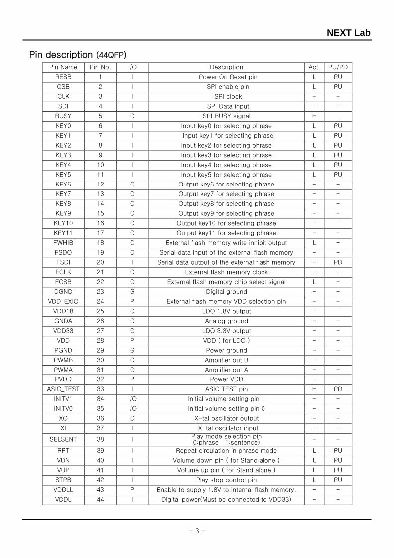
Pin description (44QFP)
Pin Name Pin No. I/O Description Act. PU/PD
RESB 1 I Power On Reset pin L PU
CSB 2 I SPI enable pin L PU
CLK 3 I SPI clock - -
SDI 4 I SPI Data input - -
BUSY 5 O SPI BUSY signal H -
KEY0 6 I Input key0 for selecting phrase L PU
KEY1 7 I Input key1 for selecting phrase L PU
KEY2 8 I Input key2 for selecting phrase L PU
KEY3 9 I Input key3 for selecting phrase L PU
KEY4 10 I Input key4 for selecting phrase L PU
KEY5 11 I Input key5 for selecting phrase L PU
KEY6 12 O Output key6 for selecting phrase - -
KEY7 13 O Output key7 for selecting phrase - -
KEY8 14 O Output key8 for selecting phrase - -
KEY9 15 O Output key9 for selecting phrase - -
KEY10 16 O Output key10 for selecting phrase - -
KEY11 17 O Output key11 for selecting phrase - -
FWHIB 18 O External flash memory write inhibit output L -
FSDO 19 O Serial data input of the external flash memory - -
FSDI 20 I Serial data output of the external flash memory - PD
FCLK 21 O External flash memory clock - -
FCSB 22 O External flash memory chip select signal L -
DGND 23 G Digital ground - -
VDD_EXIO 24 P External flash memory VDD selection pin - -
VDD18 25 O LDO 1.8V output - -
GNDA 26 G Analog ground - -
VDD33 27 O LDO 3.3V output - -
VDD 28 P VDD ( for LDO ) - -
PGND 29 G Power ground - -
PWMB 30 O Amplifier out B - -
PWMA 31 O Amplifier out A - -
PVDD 32 P Power VDD - -
ASIC_TEST 33 I ASIC TEST pin H PD
INITV1 34 I/O Initial volume setting pin 1 - -
INITV0 35 I/O Initial volume setting pin 0 - -
XO 36 O X-tal oscillator output - -
XI 37 I X-tal oscillator input - -
SELSENT 38 I Play mode selection pin 0:phrase 1:sentence) - -
RPT 39 I Repeat circulation in phrase mode L PU
VDN 40 I Volume down pin ( for Stand alone ) L PU
VUP 41 I Volume up pin ( for Stand alone ) L PU
STPB 42 I Play stop control pin L PU
VDDLL 43 P Enable to supply 1.8V to internal flash memory. - -
VDDL 44 I Digital power(Must be connected to VDD33) - -
NEXT Lab
- 4 -
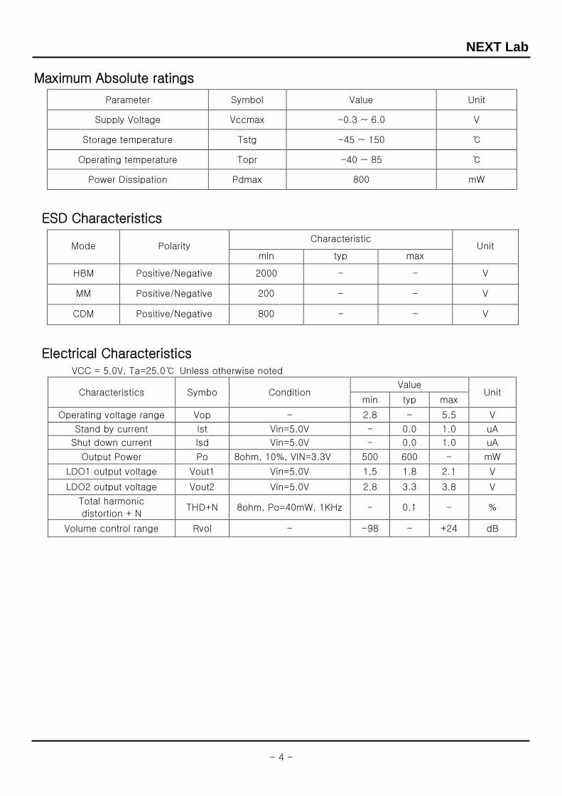
Maximum Absolute ratings
Parameter Symbol Value Unit
Supply Voltage Vccmax -0.3 ~ 6.0 V
Storage temperature Tstg -45 ~ 150 ℃
Operating temperature Topr -40 ~ 85 ℃
Power Dissipation Pdmax 800 mW
ESD Characteristics
Mode Polarity Characteristic
Unit min typ max
HBM Positive/Negative 2000 - - V
MM Positive/Negative 200 - - V
CDM Positive/Negative 800 - - V
Electrical Characteristics VCC = 5.0V, Ta=25.0℃ Unless otherwise noted
Characteristics Symbo Condition Value
Unit min typ max
Operating voltage range Vop - 2.8 - 5.5 V
Stand by current Ist Vin=5.0V - 0.0 1.0 uA
Shut down current Isd Vin=5.0V - 0.0 1.0 uA
Output Power Po 8ohm, 10%, VIN=3.3V 500 600 - mW
LDO1 output voltage Vout1 Vin=5.0V 1.5 1.8 2.1 V
LDO2 output voltage Vout2 Vin=5.0V 2.8 3.3 3.8 V
Total harmonic
distortion + N THD+N 8ohm, Po=40mW, 1KHz - 0.1 - %
Volume control range Rvol - -98 - +24 dB

NEXT Lab
- 5 -
Timing Diagram
- SPI Timing (CSB, CLK, SDI)
CSB
CLK
SDI
1 2 3 4 5 6 7 8 9 10 11 12 13 14 15 16
A7 A6 A5 A4 A3 A2 A1 A0 D7 D6 D5 D4 D3 D2 D1 D0
Tcss Tcl Tch Tcsh
Tds Tdh
Parameter Symbol 2.7 ~ 4.4V 4.5 ~ 5.5V Unit
Clock Width High Tch 500 400 ns min
Clock Width Low Tcl 500 400 ns min
Data Setup Tds 100 80 ns min
Data Hold Tdh 60 50 ns min
Select Tcss 60 50 ns min
Deselect Tcsh 120 100 ns min
- Decode timing ( Using internal flash memory mode )
td1
trep_d1
DecodingCommand
Audio Out(PWM_A/PWM_B)
The td1 is the time-gap between the stat command for decode and the real audio output.
NEXT Lab
- 6 -
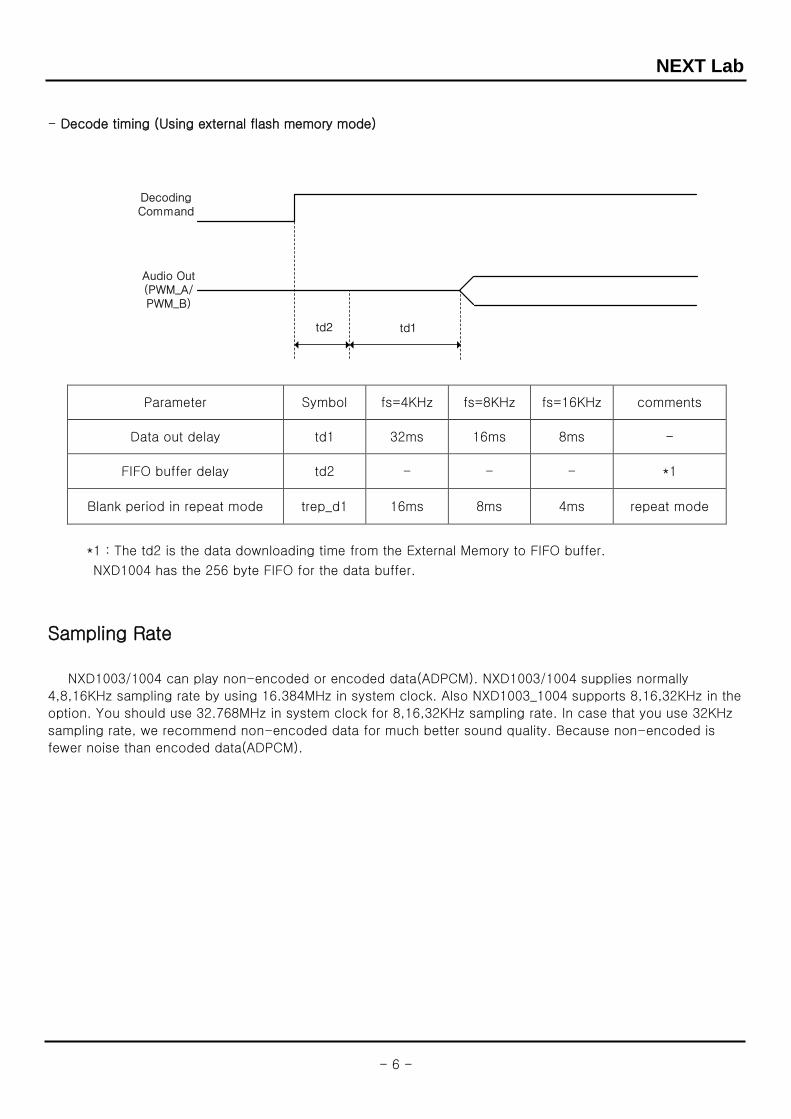
- Decode timing (Using external flash memory mode)
td1
DecodingCommand
Audio Out(PWM_A/PWM_B)
td2
Parameter Symbol fs=4KHz fs=8KHz fs=16KHz comments
Data out delay td1 32ms 16ms 8ms -
FIFO buffer delay td2 - - - *1
Blank period in repeat mode trep_d1 16ms 8ms 4ms repeat mode
*1 : The td2 is the data downloading time from the External Memory to FIFO buffer.
NXD1004 has the 256 byte FIFO for the data buffer.
Sampling Rate
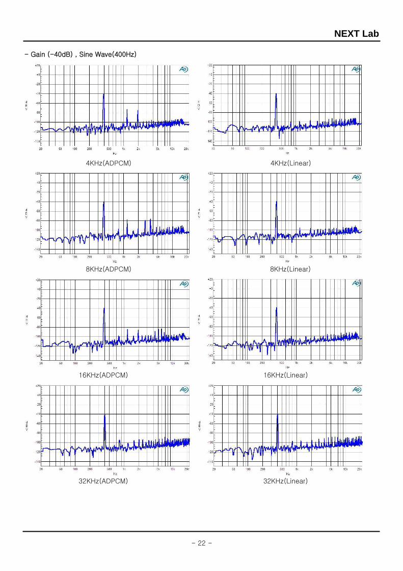
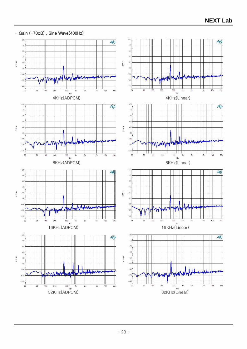
NXD1003/1004 can play non-encoded or encoded data(ADPCM). NXD1003/1004 supplies normally
4,8,16KHz sampling rate by using 16.384MHz in system clock. Also NXD1003_1004 supports 8,16,32KHz in the
option. You should use 32.768MHz in system clock for 8,16,32KHz sampling rate. In case that you use 32KHz
sampling rate, we recommend non-encoded data for much better sound quality. Because non-encoded is
fewer noise than encoded data(ADPCM).

NEXT Lab
- 7 -
Register Map
Name Addr Bit7 Bit6 Bit5 Bit4 Bit3 Bit2 Bit1 Bit0 Default
Phrase Number $E0h 0~254 Phrase / 0~31 Sentence 0x00
Volume $E1h Volume (+24~-96dB) 0x24
Control0 $E2h - Stop Repeat[1:0] OprMode[1:0] 0x00
Control1 $E3h EnDth SymDth AmtDth[1:0] EnFlt - 0x00
- Phrase Number Register ( $E0h )
This register designates the phrase number or sentence number for decoding.
- Volume Control Register ( $E1h )
This register controls the volume of the signal.
Number Volume[dB] Number Volume[dB] Number Volume[dB] Number Volume[dB]
00h +24 01h +23 02h +22 03h +21
04h +20 05h +19 06h +18 07h +17
08h +16 09h +15 0ah +14 0bh +13
0ch +12 0dh +11 0eh +10 0fh +9
10h +8 11h +7 12h +6 13h +5
14h +4 15h +3 16h +2 17h +1
18h 0 19h -1 1ah -2 1bh -3
1ch -4 1dh -5 1eh -6 1fh -7
20h -8 21h -9 22h -10 23h -11
24h -12 25h -13 26h -14 27h -15
28h -16 29h -17 2ah -18 2bh -19
2ch -20 2dh -21 2eh -22 2fh -23
30h -24 31h -25 32h -26 33h -27
34h -28 35h -29 36h -30 37h -31
38h -32 39h -33 3ah -34 3bh -35
3ch -36 3dh -37 3eh -38 3fh -39
40h -40 41h -41 42h -42 43h -43
44h -44 45h -45 46h -46 47h -47
48h -48 49h -49 4ah -50 4bh -52
4ch -54 4dh -56 4eh -58 4fh -60
50h -64 51h -68 52h -72 53h -78
54h -84 55h -90 56h -96 57h -98

NEXT Lab
- 8 -
- Control0 Register ( $E2h )
OprMode (Operating Mode) :
You can select operating Mode by setting these two bits.
0h : Nomal Play from Internal/External flash memory.
1h : Internal/External Flash Memory Program Mode.
2h : Direct Play Mode (etc. : PC control program)
Repeat :
This two bits register is for the repetition play for the selected phrase or sentence.
0h : 1-time play 1h : 2-time play
2h : 4-time play 3h : endless play until stop
Stop :
If you want to stop during playing, you can stop play by setting this register high. It is not necessary to
reset because it is internally cleared oneself.
- Control1 Register (D-Amp Control Register)
EnDth :
It will use a dither function for sound quality improvement.
0: Disable, 1: Enable
SynDth :
Select dither function mode.
0: Asymmetrical, 1: Symmetrical
AmtDth :
Set the amount of dither.
0h: 18-bit position, 1h: 17-bit position, 2h: 16-bit position, 3h 15-bit position.
Enflt :
Set the activation of fault protection function in the Speaker Block.
0: Disable, 1: Enable

NEXT Lab
- 9 -
Stand Alone Operation
Without the microprocessor, NXD1004 can operate as “Stand Alone Operation” with key pad. Stand Alone
Operation mode is judged internally without pin configuration.
- Designation of the Phrase for Decoding
It is possible to designate the phrase and sentence by using key0 ~ key11 directly. These keys must be
set with Matrix structure to designate 36 phrase or sentence. Also it can select phrase mode or sentence
mode by setting SELST pin. (0: Phrase mode, 1: Sentence mode)
When using the key switch, there is an electric and mechanical noise of the switch and this noise induce
the malfunction. To prevent this, the key inputs are not accepted during 50ms after previous key inputs.
Therefore the recommendation is to press the key over 200ms.
- Volume Control
In Stand Alone Operation, the initial volume level is controlled by the INIT0, INIT1 pin at power on time.
The volume level can be changed by selecting the level of the VUP and VDN during the power on. When
once pressing the VUP button, the 1dB level of volume will increase. When once pressing the VDN button,
the 1dB level will decrease. (Please refer to the volume chart)
INIT1 INIT0 Volume(dB)
0 0 0
0 1 -6
1 0 -12
1 1 -18
- Repetition Play the Phrase
By pushing the RPT pin`s switch, repetition play function is activated. Whenever this pin`s switch is
pushed, repetition number is change.(If this switch is pushed 4 times, repetition number is returned 1
time.)
Push Number Repetition Number
0 1
1 2
2 4
3 Infinity
- Power Save Mode
If there is no play back during over 1second in Stand Alone Operation, the operation will be changed to
the Power Save Mode automatically. To play phrase or sentence from power save mode, press any key
(key0 ~ key11). In Power Save Mode, the internal clock is stopped and also PWM outputs are off.

NEXT Lab
- 10 -
MCU Operation by SPI I/F
CSB
CLK
SDI A7 A6 A5 A4 A3 A2 A1 A0 D7 D6 D5 D4 D3 D2 D1 D0
MCU I/F Timing Chart
The above is the timing diagram of SPI interface. The structure is composed with the 8 bits address and the
8 bits data. With this SPI interface, MCU controls all the operations. The register control by using the MCU I/F
is referenced the Register Map. MCU interface protocol is automatically detected without any pin
configurations. CSB goes to High level status for next command. And this CSB signal must be High status
during minimum 3us for the stable operation of NXD1004. For the decoding operation, MCU must observe the
BUSY signal of NXD1004. When the BUSY is High, it means the internal FIFO buffer is full. If the BUSY pin is
High-level, this means that there is no space in internal FIFO buffer, therefore can not access the data.
Otherwise MCU stops the data writing for a while. If the BUSY is Low-level, MCU can write the data to the
NXD1004 for decoding.
- Power Save Mode
If there is no communication with MCU over 1second in MCU Operation, the operation will be changed
to the Power Save Mode automatically. To play phrase or sentence from Power Save Mode, please restart
to communicate with MCU. In Power Save Mode, the internal clock is stopped and also PWM outputs are
Off.
Internal / External Memory Mode
- Internal Memory Mode
For the decoding the saved ADPCM data within the internal memory, Must come to be converted in
proper format with Sampling Frequency 4/8/16KHz(8/16/32KHz). Also non-encoded data can be saved in
the internal memory, but playing time is shorter than ADPCM data. After the setting other registers
according to the necessity, the decode action will be processed with the selection of the designated
phrase. By writing the designation number to Phrase Number Register, the decoding is started.
1) When user set the “0” to the Phrase Number Register, the first phrase is selected.
2) If the designated number is greater than the maximum number of recorded, the phrase that recorded
last will be selected.
- External Memory Mode
The user can play the ADPCM or non-encoded data saved in the External Memory. It is available with
controlling the register in NXD1004 by MCU. The format of ADPCM files which are stored in the external
flash memory is compressed at 4 bit and sampling frequency 4/8/16kHz(8/16/32KHz) are possible. File
conversion is a possibility of doing with NXD1003/NXD1004 PC program. The overall sequence is same
as Play ADPCM Data. Also 16 bit PCM data must come to be converted with sameness rightly in
NXD1003/NXD1004 formats. We recommend you use non-encoded data in direct play for a quality.

NEXT Lab
- 11 -
Data Access to Internal Flash Memory
- Data download sequence
• Internal/external flash program mode setting(address E2h, data 01h)
• Flash Write protection clear operation(address 01h, data 00h)
• Flash chip erase operation(data C7h)
• Flash page program operation(Refer to figure3 on 12page.)
• Flash Write protection setting(address 01h, data 9Ch)
• Internal/external flash memory play mode setting(address E2h, data 00h)
- Write Enable(06h)
The Write Enable instruction (Figure 1) set the Write Enable Latch bit. The Write Enable Latch bit must be
set prior to every Page Program(PP), Sector Erase(SE), Block Erase(BE, Chip Erase(CE), and Write Status
Register instruction.
The Write Enable instruction is entered by driving Chip Select(CSB) low, sending the instruction code, and
then driving Chip Select(CSB) high.
CSB
CLK
SDI
Mode 0
Mode 3
Mode 0
Mode 31 2 3 4 5 6 7 8
Instruction(06h)
Figure 1. Write Enable instruction Sequence Diagram
- Write Status Register(01h)
The Write Status Register instruction allows new value to be written to the Status Register. Before it can
be accepted, a Write Enable instruction must previously have been executed. After the Write Enable
instruction has been decoded and executed, the device sets the Write Enable Latch.
The Write Status Register instruction is entered by driving Chip Select (CSB) low, followed by the
instruction code and the data byte on Serial Data Input (SDI).
The instruction sequence is shown in Figure 2.
CSB
CLK
SDI
Mode 0
Mode 3
Mode 0
Mode 31 2 3 4 5 6 7 8
Instruction(01h)
9 10 11 12 13 14 15 16
7 6 5 4 3 2 1 0
Figure2. Write Status Register Instruction Sequence Diagram
NEXT Lab
- 12 -
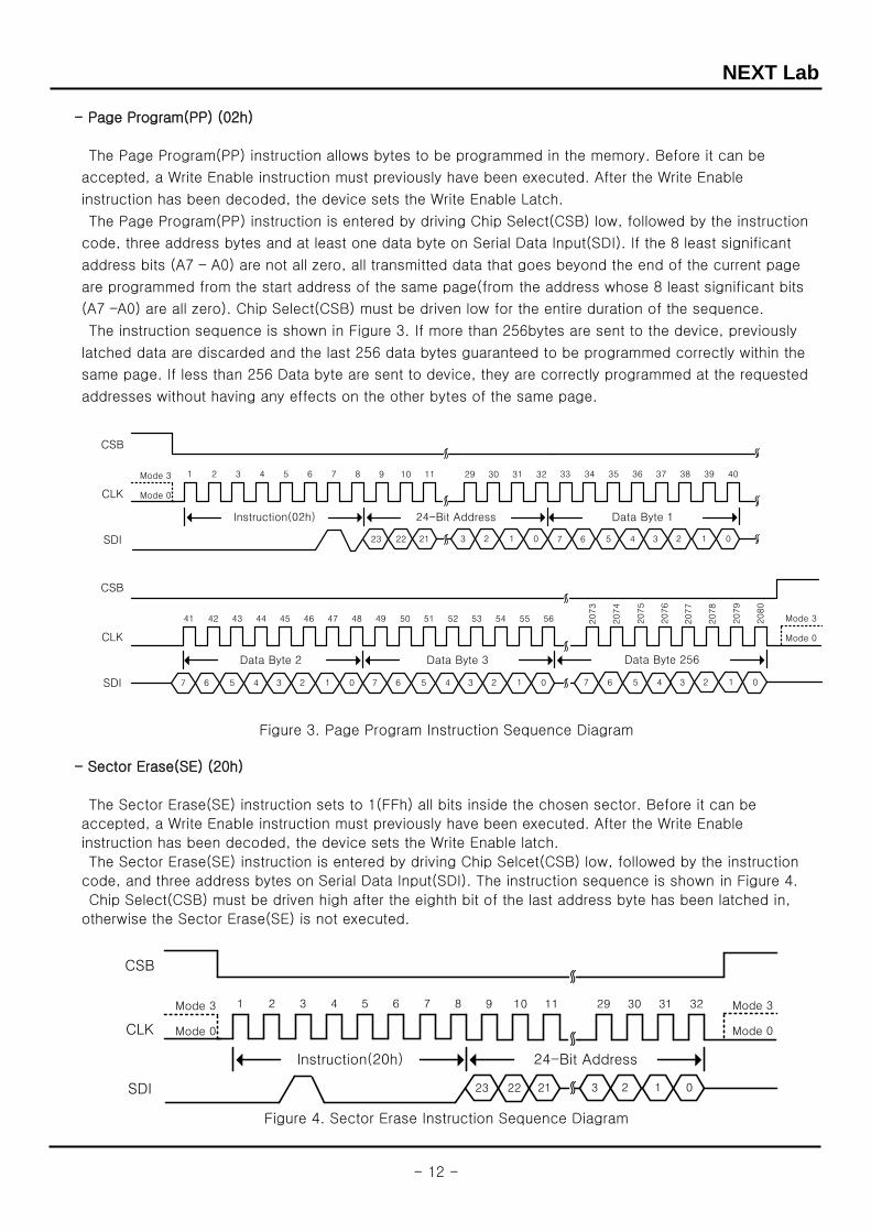
- Page Program(PP) (02h)
The Page Program(PP) instruction allows bytes to be programmed in the memory. Before it can be
accepted, a Write Enable instruction must previously have been executed. After the Write Enable
instruction has been decoded, the device sets the Write Enable Latch.
The Page Program(PP) instruction is entered by driving Chip Select(CSB) low, followed by the instruction
code, three address bytes and at least one data byte on Serial Data Input(SDI). If the 8 least significant
address bits (A7 – A0) are not all zero, all transmitted data that goes beyond the end of the current page
are programmed from the start address of the same page(from the address whose 8 least significant bits
(A7 –A0) are all zero). Chip Select(CSB) must be driven low for the entire duration of the sequence.
The instruction sequence is shown in Figure 3. If more than 256bytes are sent to the device, previously
latched data are discarded and the last 256 data bytes guaranteed to be programmed correctly within the
same page. If less than 256 Data byte are sent to device, they are correctly programmed at the requested
addresses without having any effects on the other bytes of the same page.
CSB
CLK
SDI
Mode 0
Mode 3
Mode 0
Mode 3
1 2 3 4 5 6 7 8
Instruction(02h)
9 10 11 29 30 31 32
23 22 21 3 2 1 0
24-Bit Address
33 34 35 36 37 38 39 40
Data Byte 1
7 6 5 4 3 2 1 0
7 6 5 4 3 2 1 0
CSB
CLK
SDI
41 42 43 44 45 46 47 48
Data Byte 2
49 50 51 52 53 54 55 56
Data Byte 3
7 6 5 4 3 2 1 0
2073
Data Byte 256
6 5 4 3 2 1 0
2074
2075
2076
2077
2078
2079
2080
7
Figure 3. Page Program Instruction Sequence Diagram
- Sector Erase(SE) (20h)
The Sector Erase(SE) instruction sets to 1(FFh) all bits inside the chosen sector. Before it can be
accepted, a Write Enable instruction must previously have been executed. After the Write Enable
instruction has been decoded, the device sets the Write Enable latch.
The Sector Erase(SE) instruction is entered by driving Chip Selcet(CSB) low, followed by the instruction
code, and three address bytes on Serial Data Input(SDI). The instruction sequence is shown in Figure 4.
Chip Select(CSB) must be driven high after the eighth bit of the last address byte has been latched in,
otherwise the Sector Erase(SE) is not executed.
CSB
CLK
SDI
Mode 0
Mode 3 1 2 3 4 5 6 7 8
Instruction(20h)
9 10 11 29 30 31 32
23 22 21 3 2 1 0
24-Bit Address
Mode 0
Mode 3
Figure 4. Sector Erase Instruction Sequence Diagram

NEXT Lab
- 13 -
- Block Erase(BE) (D8h)
The Block Erase(BE) instruction sets to 1 (FFh) all bits inside the chosen block. Before it can be
accepted, a Write Enable instruction must previously have been executed. After the Write Enable
instruction has been decoded, the device sets the Write Enable latch.
The Block Erase(BE) instruction is entered by driving Chip Select(CSB) low, followed by the instruction
code, and three address bytes on Serial Data Input(SDI).
The instruction sequence is shown in Figure 5. Chip Select(CSB) must be driven high after the eighth bit
of the last address byte has been latched in, otherwise the Block Erase(BE) is not executed.
CSB
CLK
SDI
Mode 0
Mode 3 1 2 3 4 5 6 7 8
Instruction(D8h)
9 10 11 29 30 31 32
23 22 21 3 2 1 0
24-Bit Address
Mode 0
Mode 3
Figure 5. Block Erase Instruction Sequence Diagram
- Chip Erase(CE) (C7h)
The Chip Erase(CE) instruction sets all bits to 1(FFh). Before it can be accepted, a Write Enable
instruction must previously have been executed. After the Write Enable instruction has been decoded, the
device sets the Write Enable latch.
The Chip Erase(CE) instruction is entered by driving Chip Select(CSB) low, followed by the instruction
code on Serial Data Input(SDI). Chip Select(CSB) must be driven low for the entire duration of the
sequence.
The instruction sequence is shown Figure 6. Chip Select(CSB) must be driven high after the eighth bit of
the instruction code has been latched in, otherwise the Chip Erase instruction is not executed.
CSB
CLK
SDI
Mode 0
Mode 3
Mode 0
Mode 31 2 3 4 5 6 7 8
Instruction(C7h)
Figure 6. Chip Erase Instruction Sequence Diagram
NEXT Lab
- 14 -
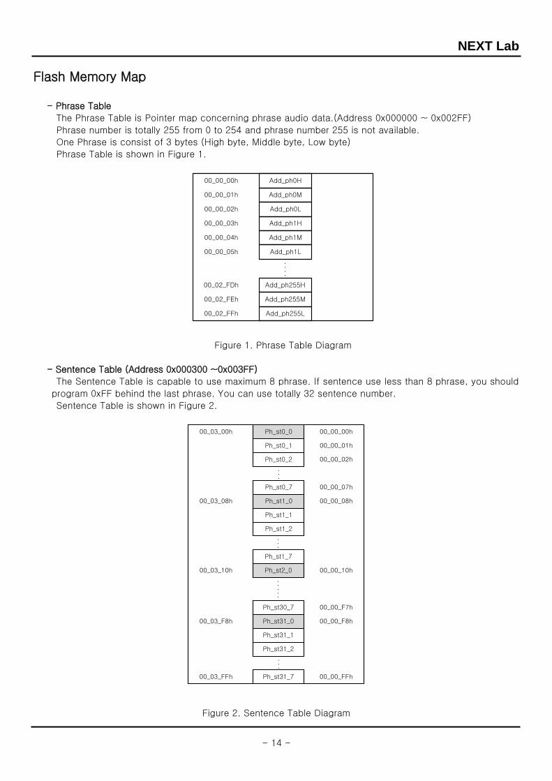
Flash Memory Map
- Phrase Table
The Phrase Table is Pointer map concerning phrase audio data.(Address 0x000000 ~ 0x002FF)
Phrase number is totally 255 from 0 to 254 and phrase number 255 is not available.
One Phrase is consist of 3 bytes (High byte, Middle byte, Low byte)
Phrase Table is shown in Figure 1.
Add_ph0H
Add_ph0M
Add_ph0L
Add_ph1H
Add_ph1M
Add_ph1L
Add_ph255H
Add_ph255M
Add_ph255L
00_00_00h
00_00_01h
00_00_02h
00_00_03h
00_00_04h
00_00_05h
00_02_FDh
00_02_FEh
00_02_FFh
Figure 1. Phrase Table Diagram
- Sentence Table (Address 0x000300 ~0x003FF)
The Sentence Table is capable to use maximum 8 phrase. If sentence use less than 8 phrase, you should
program 0xFF behind the last phrase. You can use totally 32 sentence number.
Sentence Table is shown in Figure 2.
Ph_st0_0
Ph_st0_1
Ph_st0_2
Ph_st0_7
Ph_st1_0
Ph_st1_7
Ph_st2_0
00_03_00h
00_03_08h
00_03_10h
00_03_F8h
Ph_st1_1
Ph_st1_2
Ph_st30_7
Ph_st31_0
Ph_st31_1
Ph_st31_2
Ph_st31_700_03_FFh
00_00_00h
00_00_01h
00_00_02h
00_00_07h
00_00_08h
00_00_10h
00_00_F7h
00_00_F8h
00_00_FFh
Figure 2. Sentence Table Diagram
NEXT Lab
- 15 -
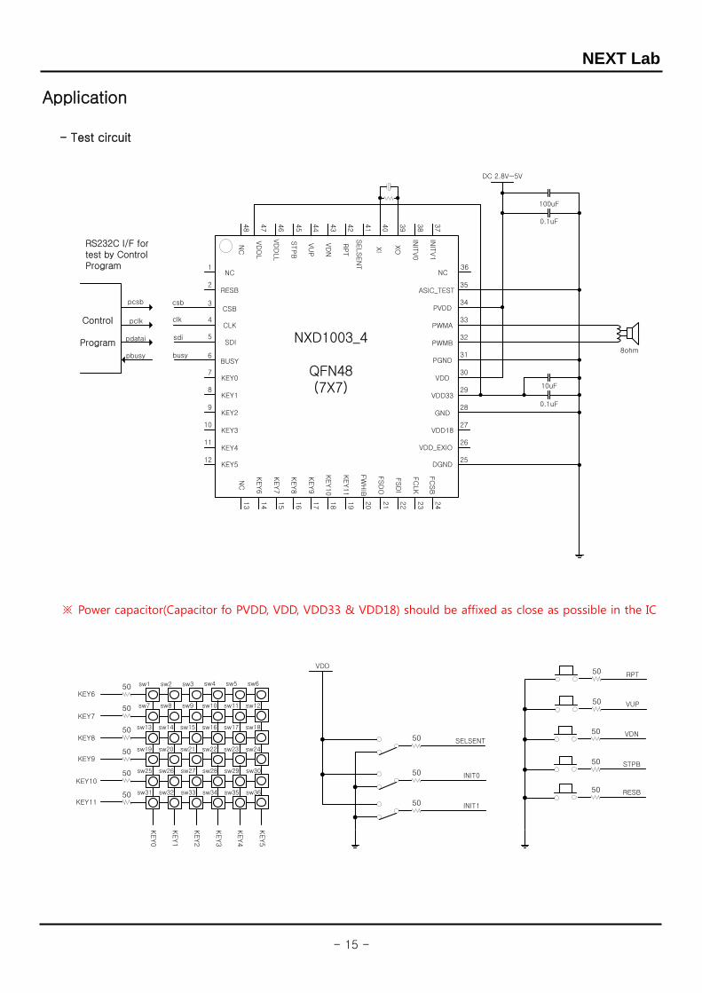
Application
- Test circuit
KEY0
KEY2
KEY1
KEY3
KEY5
KEY4
CSB
CLK
SDI
BUSY
RESB
FC
SB
FC
LK
FSD
I
FSD
O
FW
HIB
KEY6
KEY8
KEY7
KEY9
KEY11
KEY10
PVDD
PWMA
PWMB
PGND
VDD
VDD33
GND
VDD18
DGND
ASIC_TEST
VDD_EXIO
STPB
VD
N
RPT
SELSEN
T
VU
P
XOXI
INIT
V1
INIT
V0
VD
DL
VD
DLL
2
3
4
5
6
7
8
9
10
11
12
14
15
16
17
18
19
20
21
22
23
24
25
26
27
28
29
30
31
32
33
34
35
37
38
39
40
41
42
43
44
45
46
47
NXD1003_4
QFN48(7X7) 10uF
8ohm
DC 2.8V~5V
100uF
0.1uF
pcsb
pclk
pdatai
pbusy
csb
clk
sdi
busy
0.1uF
Control
Program
RS232C I/F for test by Control Program
NC1
NC
48
NC36
NC
13
※ Power capacitor(Capacitor fo PVDD, VDD, VDD33 & VDD18) should be affixed as close as possible in the IC
KEY0
KEY1
KEY2
KEY3
KEY4
KEY5
KEY6
KEY7
KEY8
KEY9
KEY10
KEY11
VDD
50
50
50 INIT1
INIT0
SELSENT
RPT
50
50
50 STPB
VDN
VUP
50
50
50
50
50
5050 RESB
50
sw1 sw2 sw3 sw4 sw5 sw6
sw7 sw8 sw9 sw10 sw11 sw12
sw13 sw14 sw15 sw16 sw17 sw18
sw19 sw20 sw21 sw22 sw23 sw24
sw25 sw26 sw27 sw28 sw29 sw30
sw31 sw32 sw33 sw34 sw35 sw36
NEXT Lab
- 16 -
1
2
3
4
5
6
7
8
9
10
11
12
13
14
15
16
17
18
19
20
21
22
23
24
25
100
100
100
100
pbusy
pcsb
pclk
psdi
100pF
OEB1
A1
A2
A3
A4
A5
A6
A7
A8
GND
VCC
OEB2
Y1
Y2
Y3
Y4
Y5
Y6
Y7
Y8
VDDpcsb
pclk
psdi
busy
csb
clk
sdi
pbusy74LVC541
100pF
500K
VDD = 5V
10K
VCC33
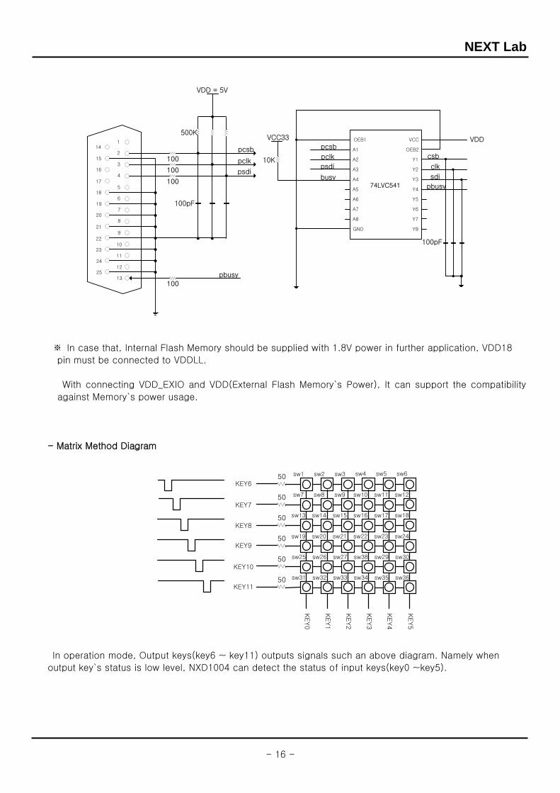
※ In case that, Internal Flash Memory should be supplied with 1.8V power in further application, VDD18
pin must be connected to VDDLL.
With connecting VDD_EXIO and VDD(External Flash Memory`s Power), It can support the compatibility
against Memory`s power usage.
- Matrix Method Diagram
KEY0
KEY1
KEY2
KEY3
KEY4
KEY5
KEY6
KEY7
KEY8
KEY9
KEY10
KEY11
50
50
50
50
50
50
sw1 sw2 sw3 sw4 sw5 sw6
sw7 sw8 sw9 sw10 sw11 sw12
sw13 sw14 sw15 sw16 sw17 sw18
sw19 sw20 sw21 sw22 sw23 sw24
sw25 sw26 sw27 sw38 sw29 sw30
sw31 sw32 sw33 sw34 sw35 sw36
In operation mode, Output keys(key6 ~ key11) outputs signals such an above diagram. Namely when
output key`s status is low level, NXD1004 can detect the status of input keys(key0 ~key5).

NEXT Lab
- 17 -
- External Flash Memory SPI I/F Diagram
External FlashMemory
CS#
VSS
DO
WP#
VCC
DI
HOLD#
CLK
*VCC =
22
21
19
18
20
FCSB
FCLK
24
1
2
3
4
8
7
6
5
FSDO
FSDI
FWHIB
VDD_EXIO
FCSB
FWHIB FCLK
FSDO
FSDI
VDD_EXIO
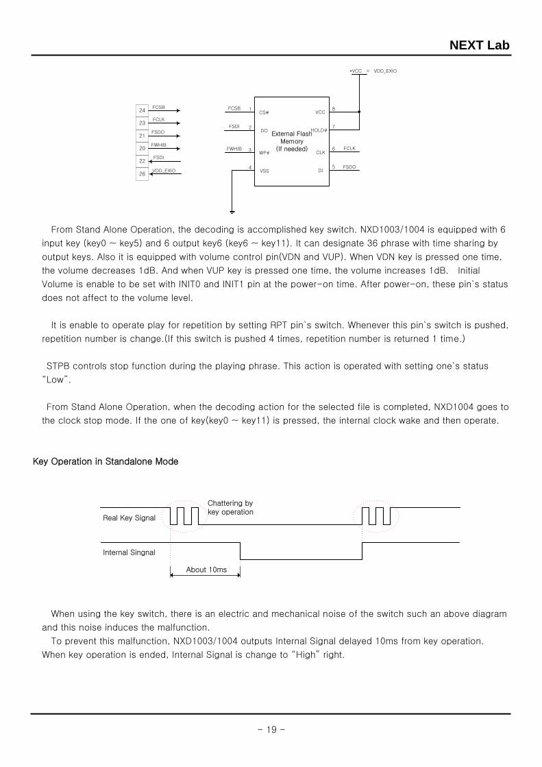
*If you need to use External Flash Memory, you must set-up this form.
※ VDD pin(External Flash Memory Power) must be connected with VDD_EXIO pin to avoid problem about
the confusion between internal VDD and external VDD.
- X-tal usage recommendation
In case of using X-tal (We recommend that you should use this method as possible.)
300kohm 16.384MHZ or 32.768MHz
XI
XO
In case of using system clock (Recommended Frequency Fr = 16.384MHz or 32.768MHz)
XI
System clock(16.384MHZ or 32.768MHz)
* If clock is being used in the system, NXD1003/1004 can use this clock source directly with connecting to XI pin.
In case of using resistor and capacitor
XO
XI
24pF
1Kohm
NEXT Lab
- 18 -
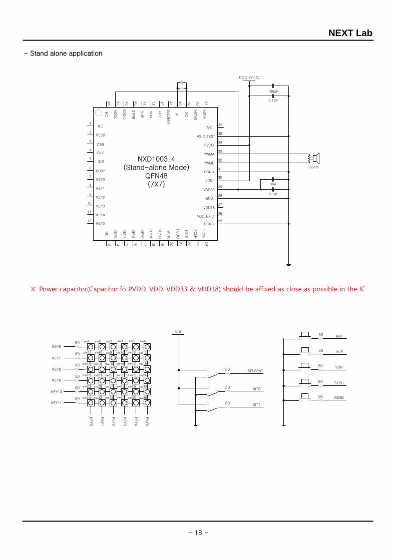
- Stand alone application
10uF
8ohm
DC 2.8V~5V
100uF
0.1uF
0.1uF
KEY0
KEY2
KEY1
KEY3
KEY5
KEY4
CSB
CLK
SDI
BUSY
RESB
FC
SB
FC
LK
FSD
I
FSD
O
FW
HIB
KEY6
KEY8
KEY7
KEY9
KEY11
KEY10
PVDD
PWMA
PWMB
PGND
VDD
VDD33
GND
VDD18
DGND
ASIC_TEST
VDD_EXIO
STPB
VD
N
RPT
SELSEN
T
VU
P
INIT
V1
INIT
V0
VD
DL
VD
DLL
2
3
4
5
6
7
8
9
10
11
12
14
15
16
17
18
19
20
21
22
23
24
25
26
27
28
29
30
31
32
33
34
35
37
38
41
42
43
44
45
46
47
NXD1003_4(Stand-alone Mode)
QFN48(7X7)
NC1
NC
48
NC36
NC
13
XOXI
39
40
※ Power capacitor(Capacitor fo PVDD, VDD, VDD33 & VDD18) should be affixed as close as possible in the IC
KEY0
KEY1
KEY2
KEY3
KEY4
KEY5
KEY6
KEY7
KEY8
KEY9
KEY10
KEY11
VDD
50
50
50 INIT1
INIT0
SELSENT
RPT
50
50
50 STPB
VDN
VUP
50
50
50
50
50
5050 RESB
50
sw1 sw2 sw3 sw4 sw5 sw6
sw7 sw8 sw9 sw10 sw11 sw12
sw13 sw14 sw15 sw16 sw17 sw18
sw19 sw20 sw21 sw22 sw23 sw24
sw25 sw26 sw27 sw28 sw29 sw30
sw31 sw32 sw33 sw34 sw35 sw36
NEXT Lab
- 19 -
External FlashMemory
(If needed)
CS#
VSS
DO
WP#
VCC
DI
HOLD#
CLK
*VCC =
24
23
21
20
22
FCSB
FCLK
26
1
2
3
4
8
7
6
5
FSDO
FSDI
FWHIB
VDD_EXIO
FCSB
FWHIB FCLK
FSDO
FSDI
VDD_EXIO
From Stand Alone Operation, the decoding is accomplished key switch. NXD1003/1004 is equipped with 6
input key (key0 ~ key5) and 6 output key6 (key6 ~ key11). It can designate 36 phrase with time sharing by
output keys. Also it is equipped with volume control pin(VDN and VUP). When VDN key is pressed one time,
the volume decreases 1dB. And when VUP key is pressed one time, the volume increases 1dB. Initial
Volume is enable to be set with INIT0 and INIT1 pin at the power-on time. After power-on, these pin`s status
does not affect to the volume level.
It is enable to operate play for repetition by setting RPT pin`s switch. Whenever this pin`s switch is pushed,
repetition number is change.(If this switch is pushed 4 times, repetition number is returned 1 time.)
STPB controls stop function during the playing phrase. This action is operated with setting one`s status
“Low”.
From Stand Alone Operation, when the decoding action for the selected file is completed, NXD1004 goes to
the clock stop mode. If the one of key(key0 ~ key11) is pressed, the internal clock wake and then operate.
Key Operation in Standalone Mode
About 10ms
Chattering by key operation
Internal Singnal
Real Key Signal
When using the key switch, there is an electric and mechanical noise of the switch such an above diagram
and this noise induces the malfunction.
To prevent this malfunction, NXD1003/1004 outputs Internal Signal delayed 10ms from key operation.
When key operation is ended, Internal Signal is change to “High” right.
NEXT Lab
- 20 -
- MCU application
0.1uF
DC 2.8V~5V
100uF
0.1uF
SPI I/F for Control
Switch for selecting phrase or sentence mode.
MCU
10uFKEY0
KEY2
KEY1
KEY3
KEY5
KEY4
CSB
CLK
SDI
BUSY
RESB
FC
SB
FC
LK
FSD
I
FSD
O
FW
HIB
KEY6
KEY8
KEY7
KEY9
KEY11
KEY10
PVDD
PWMA
PWMB
PGND
VDD
VDD33
GND
VDD18
DGND
ASIC_TEST
VDD_EXIOSTPB
VD
N
RPT
SELSEN
T
VU
P
INIT
V1
INIT
V0
VD
DL
VD
DLL
2
3
4
5
6
7
8
9
10
11
12
14
15
16
17
18
19
20
21
22
23
24
25
26
27
28
29
30
31
32
33
34
35
37
38
41
42
43
44
45
46
47
NXD1003_4(MCU Mode)
QFN48(7X7)
NC1
NC
48
NC36
NC
13
XOXI
39
40
8ohm
MCU_VDD
50kohm
※ Power capacitor(Capacitor fo PVDD, VDD, VDD33 & VDD18) should be affixed as close as possible in the IC
※Caution
There is no need the pull-up resistor for KEY0~KEY5 pin.
Because NXD1003/1004 has internally pull-up for these, therefore if you connect to ground(GND),
the unwanted current flows and increases the power consumption.
If you want to play phrase and sentence by turns, MCU should control SELSENT(41). If the status of
SELSENT is changed, it is applied from next turn.
External FlashMemory
(If needed)
CS#
VSS
DO
WP#
VCC
DI
HOLD#
CLK
*VCC =
24
23
21
20
22
FCSB
FCLK
26
1
2
3
4
8
7
6
5
FSDO
FSDI
FWHIB
VDD_EXIO
FCSB
FWHIB FCLK
FSDO
FSDI
VDD_EXIO

NEXT Lab
- 21 -
FFT Waveform - Gain (-10dB) , Sine Wave(400Hz)
4KHz(ADPCM) 4KHz(Linear)
8KHz(ADPCM) 8KHz(Linear)
16KHz(ADPCM) 16KHz(Linear)
32KHz(ADPCM) 32KHz(Linear)
NEXT Lab
- 22 -
- Gain (-40dB) , Sine Wave(400Hz)
4KHz(ADPCM) 4KHz(Linear)
8KHz(ADPCM) 8KHz(Linear)
16KHz(ADPCM) 16KHz(Linear)
32KHz(ADPCM) 32KHz(Linear)
NEXT Lab
- 23 -
- Gain (-70dB) , Sine Wave(400Hz)
4KHz(ADPCM) 4KHz(Linear)
8KHz(ADPCM) 8KHz(Linear)
16KHz(ADPCM) 16KHz(Linear)
32KHz(ADPCM) 32KHz(Linear)

NEXT Lab
- 24 -
Package Dimensions <36SSOP>
NEXT Lab
- 25 -
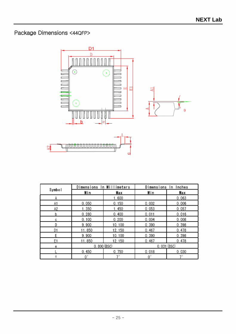
Package Dimensions <44QFP>