fe in iii-v and ii-vi semiconductors · models mentioned above. many experimental and theoretical...
TRANSCRIPT

© 2008 WILEY-VCH Verlag GmbH & Co. KGaA, Weinheim
phys. stat. sol. (b), 1–26 (2008) / DOI 10.1002/pssb.200743315
Early View publication on www.interscience.wiley.com (issue and page numbers not yet assigned; citable using Digital Object Identifier – DOI)
Review Article
p s sbasic solid state physics
b
statu
s
soli
di
www.pss-b.comph
ysi
ca
Fe in III–V and II–VI semiconductors
Enno Malguth*, 1, 2, Axel Hoffmann1, and Matthew R. Phillips2
1 Institut für Festkörperphysik, Technische Universität Berlin, Hardenbergstraße 36, 10623 Berlin, Germany 2 Microstructural Analysis Unit, University of Technology, Sydney, Broadway, NSW 2007, Australia
Received 11 July 2007, revised 7 November 2007, accepted 20 November 2007
Published online 1 February 2008
PACS 71.70.Ej, 71.70.Gm, 75.50.Pp, 76.30.Fc, 78.40.Fy
* Corresponding author: e-mail [email protected], Phone: +49-30-31424440, Fax: +49-30-31422064
© 2008 WILEY-VCH Verlag GmbH & Co. KGaA, Weinheim
1 Introduction 1.1 Application and motivation The Fe impurity in III–V and II–VI compound semi-conductors has been the subject of research for several decades. In the past, it was studied as an inevitable defect providing experimental information of interest for aspects of group theory. Fe is also introduced deliberately into semiconductor materials used in electronic and optoelectronic devices to achieve semi-insulating substrate material [1]. Today though, transition metal (TM) doped semicon-ductors are the major subject of recent attempts to realize ferromagnetic semiconductors for spintronics applica-tions [2–9]. Such alloys represent dilute magnetic semi-conductors (DMS). Potential mechanisms of a ferromag-netic coupling between the isolated TM ions are superex-
change, double-exchange [10], kinetic exchange and an in-teraction involving bound magnetic polarons [4, 8]. In par-ticular in the wide gap materials GaN and ZnO, a high po-tential to eventually achieve room temperature ferromag-netism through kinetic exchange in the form of hole medi-ated spin-coupling has been predicted (Zener model) [6]. Microscopically, the spin-coupling between the free carri-ers and the localized TM centers is established by ex-change interaction. This approach requires high concentra-tions of TM ions and holes at the same time [6]. Also the charge state of the TM center is a critical parameter of the models mentioned above. Many experimental and theoretical studies (mainly fo-cussed on Mn) lack a comprehensive, quantitative under-standing of the electronic structure of the TM centers. In
Many theoretical and experimental studies deal with the reali-
zation of room-temperature ferromagnetism in dilute mag-
netic semiconductors (DMS). However, a detailed quantita-
tive understanding of the electronic properties of transition
metal doped semiconductors has often been neglected. This
article points out which issues concerning electronic states
and charge transfers need to be considered using Fe as an ex-
ample. Methods to address these issues are outlined, and a
wealth of data on the electronic properties of Fe doped III–V
and II–VI compound semiconductors that have been obtained
over a few decades is reviewed thoroughly. The review is
complemented by new results on the effective-mass-like state
consisting of a hole bound to Fe2+ forming a shallow acceptor
state.
The positions of established Fe3+/2+ and Fe2+/1+ charge transfer
levels are summarized and predictions on the positions of
further charge transfer levels are made based on the internal
reference rule. The Fe3+/4+ level has not been identified
unambiguously in any of the studied materials. Detailed term
schemes of the observed charge states in tetrahedral
and trigonal crystal field symmetry are presented including
hyperfine structure, isotope effects and Jahn–Teller effect.
Particularly, the radiative transitions Fe3+(4T1 → 6A1) and
Fe2+(5E → 5T2) are analyzed in great detail.
An effective-mass-like state [Fe2+, h] consisting of a hole
bound to Fe2+ is of great significance for a potential realiza-
tion of spin-coupling in a DMS. New insights on this shallow
acceptor state could be obtained by means of stress dependent
and temperature dependent absorption experiments in the mK
range. The binding energy and effective Bohr radius were
determined for GaN, GaP, InP and GaAs and a weak ex-
change interaction between the hole and the Fe2+ center was
detected.
With regard to the Fe3+ ground state, 6A1, in GaP and InP, the
hyperfine structure level 8
Γ was found to be above the 7
Γ
level.
All results are discussed with respect to a potential realization
of a ferromagnetic spin-coupling in DMSs.

2 E. Malguth et al.: Fe in III–V and II–VI semiconductors
© 2008 WILEY-VCH Verlag GmbH & Co. KGaA, Weinheim www.pss-b.com
ph
ysic
ap s sstat
us
solid
i b
this paper, we summarize such experimental data of the Fe center in a wide range of III–V and II–VI host materials. Our goal is to provide crucial information required for an estimate of the feasibility of an Fe based DMS. We shall point out common phenomena that can be generalized to other TM’s. In order to gauge the potential of an Fe-doped semi-conductor for a ferromagnetic coupling, the following questions need to be answered: (1) Which charge states of Fe are found and what states do they form within the band gap of the host material, especially near (~20 meV) the electronic bands? (2) What is the position of the charge transfer (donor or acceptor) levels? (3) Do we observe any type of interaction between the Fe center and itinerant car-riers that might enable spin-coupling? Those three questions are addressed in detail through-out this paper. On the basis of optical and magnetic studies, complete term schemes of Fe3+ (Section 3.2) and Fe2+ (Section 3.3) are established and the charge transfer energies are given as far as they are known (Section 2). Regarding the last question, we present new results on the shallow hydrogenic state consisting of a hole localized at Fe2+ (Section 4) that are significant in the context of spin-coupling via bound magnetic polarons [11]. 2 Charge transfer levels In order to gauge the fea-sibility of an Fe based DMS it is most important to know the position of the charge transfer (CT) levels, i.e., donor and acceptor levels, formed by the Fe impurity.
2.1 Significance of charge transfer levels A transfer from one charge state of Fe into another can be es-
Enno Malguth is a Ph.D. student at the Institut für Fest-körperphysik, Technische Universität Berlin and at the Microstructural Analysis Unit, University of Technol-ogy Sydney. His main field of research is the optical and magnetic characterization of transitional-metal-doped wide-band-gap semiconductors for potential spin-tronic applications. By the time of publication, he will have finished his Ph.D. and is starting a position as a postdoctoral fellow at the School of Electrical and Computer Engineering at the Georgia Institute of Tech-nology where he wants to extend his research onto the growth of ferromagnetic semiconductors.
tablished by transferring a d-electron from the Fe center into one of the bands of the host lattice or vice versa. The energy involved in this charge transfer process is the charge transfer energy and can be identified with a level within the band gap (see Fig. 1). The Fe ( 1)N N/ - and Fe ( 1)N N/ + levels represent deep acceptor 0
A/- and donor 0
D/+ states,
respectively. N is the charge state of the isoelectronic case. For Fe on cation site, N is 3+ and 2+ for III–V and II–VI compounds, respectively. The CT levels ( 1)
FeN N/ - and
( 1)Fe
N N/ + are usually found above and below the middle of the band gap, respectively. However, their exact position also depends on the stability of the involved charge states. For instance, the high correlation energy of the stable 5
d configuration of Fe3+ shifts the Fe3 2+/ + level to higher and the Fe3 4+/ + level to lower energies (Fig. 1). In general, there is only one charge state present at equilibrium conditions. Which one that is depends on the position of the Fermi level in relation to the CT levels (Fig. 1). In thermodynamic equilibrium, the position of the Fermi level is a function of donor and acceptor concentra-tions and therefore may again depend on the Fe concentra-tion [12]. In the case of high Fe concentrations needed for the potential realization of a ferromagnetic semiconductor, the position of the Fermi level may be governed mainly by the Fe impurity. Consequently, two charge states could be present pinning the Fermi level to the respective CT level. As the Fe3 2+/ + CT level is found near the middle of the band gap in most materials, this effect is exploited by heavy Fe-doping for producing semi-insulating material that is needed as substrate for electronic and optoelectronic devices [1]. Other charge states may be created (activated) in non-equilibrium conditions. For instance, optical excitation may induce a charge transfer either directly in the form of a Fe center to band transition or by producing free carriers, i.e., shifting the Fermi level. Optically induced CT transi-tions starting from the isoelectric charge state are called photoionization, the ones terminating at it photo neutraliza-tion. From the just discussed meaning of the position of the CT levels their significance in the context of ferromagnetic DMS’s becomes apparent. The charge state and the result-ing spin of the Fe center are crucial points when calculat-ing a potential ferromagnetic coupling [8]. Hence, in order to make predictions on or achieve a particular charge state, the position of the CT levels needs to be known as pre-cisely as possible. The donor and acceptor states formed by Fe may impede or support p- or n-doping. The promising approach of hole mediated spin-coupling requires high hole concentrations [6]. Here, the role of the TM center is decisive for a successful implementation. If the iron 0
A/-
level is found close to or within the VB then the Fe center will not only provide localized spin but also the required holes. However, if the 0
D/+ level is found within the band
gap it will compensate the p-doping 0(D + h → D )+ by pinning the Fermi energy, unless it is located between the VB and the acceptor level of the p-dopant.

phys. stat. sol. (b) (2008) 3
www.pss-b.com © 2008 WILEY-VCH Verlag GmbH & Co. KGaA, Weinheim
Review
Article
Fe3+/2+(A )
0/-
Fe (3+/4+
D )0/+
GaP InPGaAs
GaN
AlN
GaSb
InAs
Fe2+/1+(A )
-/--
1
0
2
3
4
5
-1
-2
Energy(eV)
III-V
InN
Fe3+
Fe2+
Fe1+
Fe4+
?
Fe3+/2+
Fe2+/1+
(a)
CB
VB
Fe2+/3+(D )
0/+
Fe2+/1+(A )
0/-
1
0
2
3
4
5
-1
-2
II-VI
ZnSZnSe
ZnTe
ZnO
CdTe
CdSCdSe
Fe1+
Fe2+
Fe3+
Fe3+/2+
Fe2+/1+
(b)
CB
VB
Energy(eV)
Figure 1 Charge transfer levels Fe2 1,
+/ + Fe3 2+/ + and Fe3 4+/ + in (a) III–V and (b) II–VI compounds. The band gaps and band off-sets
were taken from [15, 16]. For recently established values of the band gap of InN, see Refs. [17, 18] and references therein. The CT
values were taken from Table 1. Dark grey bars roughly indicate trends of common Fe levels according to the internal reference
rule [13, 14]. They separate energy regimes of stable oxidation states. Regarding the II–VI materials (b), the potential trends are dif-
ferent for Zn and Cd compounds. The position of the Fe3 4+/ + level in III–V materials is still unclear.
Additionally, the position of the CT levels is also needed to place the term schemes of the single charge states that are established in Section 3 in the correct rela-tion to the bands. It is also important regarding the internal reference rule that predicts band off-sets in semiconductor hetero-structures on the basis of TM CT levels [13, 14]. 2.2 Determining the position of the CT levels The position of the CT levels can be determined from ob-serving the CT process (photoionization) in absorption, PL excitation, photo conductivity or photo ESR experiments where it appears as an exponentially rising band (see Figs. 2 and 9). The underlying processes were modeled successfully by Ridley et al. [19–21]. The low-energy on-set of that band is the photoionization threshold and equals the distance between the CT level and the involved band.
The values obtained this way are relatively inaccurate because the exact photoionization threshold is difficult to pinpoint. A more accurate method exploiting the effective-mass-like state [Fe2+, h] is presented in Section 4.3.3. Between two charge states, two CT processes can be observed in photoionization experiments:
1
1 VBFe Fe h ,
N Nhν
-
+ Æ + (1)
1
2 CBFe Fe e .
N Nhν
-
+ Æ + (2)
Due to its s–d character transitions involving the s-like CB (Eq. (2)) have a much smaller oscillator strength and are more difficult to detect than those involving the p-like VB (Eq. (1)). In ZnS an energy transfer from one Fe2+ ion to another was observed in the form [22]
2 3 2 3 1
CB2Fe Fe e Fe Fe Fe .hν
+ + + + +
+ Æ + + Æ + (3)
0.5 1.0 1.5
Absorption(arb.units)
Energy (eV)
GaAs:Fe
GaP:Fe
InP:Fe
IIIIII
E5
5T2
Fe2+
Fe3+
I
II
III
VB
CB
+
Figure 2 Typical absorption spectra of semi-insulating InP, GaAs and GaP. All spectra exhibit the internal Fe2+(5E → 5T2) transition
(I) and two charge transfer bands (II and III) representing 3 2Fe Fe
+ +
Æ CT processes that result in the Fe2+(5E) ground and Fe2+(5T2)
excited state, respectively, while a hole is generated in the VB. The energy diagram on the right illustrates these three transitions.

4 E. Malguth et al.: Fe in III–V and II–VI semiconductors
© 2008 WILEY-VCH Verlag GmbH & Co. KGaA, Weinheim www.pss-b.com
ph
ysic
ap s sstat
us
solid
i b
It should be noted that, in general, the sum of the CT energies
1hν and
2hν (Eqs. (1) and (2)) does not equal the
band gap energy because of lattice relaxation effects [23, 24]. In extreme cases these effects may be of magnitudes up to 0.3 eV [24]. Another issue of determining the CT level from photoionization spectra is that the observed CT process might be that of another defect and that the Fe charge state is simply changed by the free carriers created in that first process [12, 25]. The experimentally found CT levels are summarized in Table 1 and in Fig. 1. The CT process (Eq. (1)) terminating in both the 5E and the 5T
2 states of Fe2+ has been observed
in InP, GaAs, GaP and GaN (see Figs. 2 and 9) [12, 34]. Unfortunately, the Fe3 2+/ + level in ZnO has not been found to date although both charge states 3+ and 2+ have been observed [25, 35]. Here, the problem is that the holes that establish the CT process are generated via different defects at 2.25 eV [25]. While the Fe2 1+/ + level has only been ob-served in GaP and ZnS [26, 29] it must be found within the band gap of ZnSe, ZnTe and CdTe as well. In these mate-rials both charge states Fe2+ and Fe1+ have been identified (Sections 3.3 and 3.4). Neither the 3 4
Fe Fe+ +
´ transition nor the Fe4+ state have been observed in any material to date. Merely theoretical calculations and tentative specula-tions based on near band edge luminescence put the Fe3 4+/ + level above the VB edge in GaN and AlN [36, 37]. From Fig. 1 further conclusions about so far unob-served CT levels can be drawn if we assume the band off-sets to be correct and that the internal reference rule holds, i.e., that there is a trend in the position of the CT levels at least within related material systems. Among the III–V Table 1 Experimentally determined position of the CT levels
Fe3 2+/ + and Fe2 1.
+/ + The Fe3 4+/ + level has not been found in any
material. The values are given in meV as measured from the VB
maximum unless indicated otherwise. The values of GaP, InP and
GaAs are derived in this work with high accuracy from a com-
parison of the binding energies of the bound state [Fe2,
+ h] with
effective mass theory (Section 4.3.3). The values of the other ma-
terials were determined from the photoionization threshold. Lev-
els that have not been observed yet but that are believed to be
found within the band gap because both charge states have been
observed are labeled (gap).
material Fe3 2+/ + Ref. Fe2 1+/ +
Ref.
(meV) (meV)
GaP 851.8 [this work] ECB
240- [26]
InP 800.6 [this work]
GaAs 510.8 [this work]
GaN 2870 ± 10 [12]
AlN 3000 ± 300 [27]
ZnS ECB
2100- ± 100 [28] ECB
240- ± 100 [29]
ZnSe 890, 1250 [13, 23] (gap)
ZnTe ECB
2240- ± 50 [30] 1700 ± 50 [30]
ZnO >2250 [25]
CdTe 350, 150 [31, 32] (gap) [30]
CdS <1300 [33]
CdSe 800, 640 [13, 23]
materials in Fig. 1(a) the only other material apart from GaP where the Fe2 1+/ + level can be expected to be found within the band gap is AlN. Regardless of the exact band gap energy of InN [17, 18], Fe3+ is probably the only sta-ble charge state. Regarding the II–VI materials, if we dis-tinguish between Zn and Cd compounds we get a better agreement with the internal reference rule for each group. From the respective trends we can conclude that if the Fe2 1+/ + level is really found within the band gap of ZnSe and CdTe it must be very close to the CB. In ZnO, the Fe2 1+/ + level is very likely to be found in the CB. The posi-tion of the Fe3 2+/ + level in ZnO can be narrowed down to be between 2.25 eV and 2.8 eV above the VB and in CdS to be between 1 eV and 1.3 eV. 2.3 Implications of the found charge transfer levels From the found position of the CT levels we can conclude that the Fe3 2+/ + acceptor level in GaN is too deep to act as a hole source in a potential DMS based on hole mediated spin-coupling. Here, additional p-doping would be required. However, as discussed above, if the Fe3 4+/ + donor level turns out to be found higher than a few tens of meV above the VB it will compensate the p-doping imped-ing the realization of hole-mediated ferromagnetism. This problem is quite likely to occur in AlN (see Fig. 1). The same applies for the II–VI materials included in Fig. 1 be-cause the Fe3 2+/ + donor level is high above the VB in all of them. On the other hand, apart from GaN and AlN, the Fe3 4+/ + donor level is located well within the VB of III–V materials enabling p-doping. The only material included in Fig. 1 where Fe might act as a shallow acceptor is GaSb. In intrinsic GaN where natural defects act as donors rising the Fermi level, iron is predominantly found in the Fe2+ charge state. At high Fe concentrations with the Fermi level pinned to the Fe3 2+/ + level both charge states are pre-sent and GaN becomes semi-insulating [12]. A similar be-havior is expected for most other materials with intrinsic defects acting as donors. Regarding the validity of the internal reference rule [13, 14], it can be concluded that it holds to a certain extend in-side the three material groups Zn compounds, Cd com-pounds and phosphides/arsenides (see Fig. 1). Inside the nitrides and between these material groups it only provides a rough trend. 3 Electronic structure of the Fe charge states
The electronic structure of the different charge states of Fe occurring in III–V and II–VI semiconductors needs to be understood in order to make predictions about a potential spin-coupling. Carrier mediated spin-coupling requires free carriers to interact with the Fe centers [6]. Therefore, levels close to the bands are of particular interest which free carriers could be captured in and released from at room tempera-ture. Another mechanism of ferromagnetic coupling, double exchange, is established by d-electrons hopping between

phys. stat. sol. (b) (2008) 5
www.pss-b.com © 2008 WILEY-VCH Verlag GmbH & Co. KGaA, Weinheim
Review
Article
two isolated TM centers with different numbers of elec-trons [4, 8, 10, 38]. At large TM concentrations, partly filled itinerant impurity bands may be formed from Fe d-levels in the band gap. Both ferromagnetic coupling and electrical conduction are accomplished by hopping within these bands. No free VB or CB carriers are involved in double exchange. A good understanding of the electronic structure of all occurring Fe charge states is required for predictions about d-states potentially involved in that hop-ping process and the formation of such bands. Also the coupling mechanism involving bound magnetic polarons depends crucially on the configuration of the magnetic centers [39]. As discussed above, the charge state of the Fe center is a critical parameter in the models of carrier mediated spin-coupling. When applying optical and magnetic (e.g., elec-tron spin resonance (ESR)) techniques to determine the present charge state of a new alloy containing Fe, a deep understanding of the electronic structures of potential charge states is essential to interpret the respective results. In this section, we do not confine ourselves to the mere aspects of the electronic structure that are of interest for spin-coupling. Moreover, complete term schemes are pre-sented including hyperfine structure, isotope effects and Jahn–Teller effect. 3.1 The emergence of the electronic structure
Incorporated into the host crystal the electronic structure of the Fe center is the result of a multiple splitting of the highly degenerate states of the free ion by symmetry reduc-tion (Figs. 3 and 10). The Stark effect of the crystal field has the strongest impact. The resulting electronic structure can be approximated by the Hamiltonian
free ion CF SO v JT pert( ) ,H H H H H H H= + + + + + (4)
with the perturbation terms: free ion
H = Hamiltonian of free ion including multi electron interaction according to Hund’s rule,
CFH = crystal field (Stark effect),
SOH = spin-
orbit interaction, v
H = vibrational contributions, JT
H = electron–phonon coupling namely Jahn–Teller coupling,
pertH = possible further perturbation, e.g., axial distortion of the crystal field in hexagonal crystals (C3V symmetry). Specific term schemes of Fe 3+ and Fe 2+ illustrating the various splitting processes are shown in Figs. 3 and 10, re-spectively. III–V and II–VI materials predominantly crystalize in the cubic zincblende and the hexagonal wurtzite structure. Fe has been found to be preferably incorporated on the cation site which has a tetrahedral (
dT ) symmetry in cubic
crystals and a trigonal symmetry (C3V) in hexagonal ones [40–42]. The trigonal case can be treated as a pertur-bation of the tetrahedron in the form of a slight axial dis-tortion along the c-axis. The amplitude of the crystal field splitting is given by the crystal field parameter Dq and the spin–orbit splitting by the spin–orbit-coupling parameter λ . In this paper, Mullikan notation is used for the irre-
ducible representation of crystal field states while Bethe notation is used for spin–orbit and less degenerate states. The Fe center may suffer a Jahn–Teller effect, i.e., a spontaneous symmetry reduction by a displacement of the surrounding nuclei leading to a partial lift of degener-acy and a decreased over-all energy [43]. The energy difference between the symmetric and the distorted con-figuration is the Jahn–Teller energy
JT( ).E As there are
usually several such distorted configurations the system oscillates between them enabling a coupling to the vibrational motion of the lattice. This is called a dynami- cal Jahn–Teller effect and has a crucial impact on the electronic fine structure of the Fe center. Here,
JTE is a
measure of the strength of the coupling to vibrational modes. The eventual electronic structure can be determined experimentally by means of optical and magnetic experi-ments. The position of the term schemes within the band gap, i.e., the relation to the bands, infers from the the re-spective CT level which equals the position of the ground state.
6A1
4G
6S
Hfree ion HCF(Td) HSO HJT
4D
4P
4F
4 4A , E1
4T1
4T2
Γ8
Γ8
Γ7
Γ6
Γ8, Γ6Γ8, Γ7
Γ8, Γ7
Figure 3 Qualitative term scheme of the Fe3+ center in a tetrahe-
dral crystal field. The hamiltonian of the isolated ion and terms
for the crystal field, spin–orbit interaction and Jahn–Teller effect
are given at the bottom. The case of a trigonal crystal field of a
hexagonal lattice is outlined in Fig. 8. The energetic differences
are not to scale.

6 E. Malguth et al.: Fe in III–V and II–VI semiconductors
© 2008 WILEY-VCH Verlag GmbH & Co. KGaA, Weinheim www.pss-b.com
ph
ysic
ap s sstat
us
solid
i b
3.2 The Fe 3+ center Fe 3+ has a 53d configuration.
Consequently, the free ion has a 6S ground state and a 4G first excited state (see Fig. 3). Under the impact of the
dT
crystal field, the first transforms into a 6A1 state and the
latter splits into four states of 4T1, 4
2T , 4E and 4A
1 symme-
try, in order of rising energy. Compared to the free ion, the energy difference between the crystal field states is re-duced by the partially covalent bonding. The crystal field states are further split by spin–orbit coupling. The 4T
1 state splits into four states of
6Γ ,
8Γ ,
7Γ and
8Γ sym-
metry. The 6A1 ground state is split neither by the crystal
field nor by the spin–orbit coupling because of its singlet character. Only spin–spin interaction and second order spin–orbit terms lead to a splitting of a few µeV, into a
8Γ
and a 7
Γ state the energetic order of which is elucidated in Section 4.3.3. Beyond spin–orbit coupling, the Fe3+ states are also affected by symmetry reduction such as the axial distortion of the crystal field of hexagonal crystals and the Jahn–Teller effect. Since Mn2+ and Cr+ also have 5
d con-figuration these ions exhibit a similar splitting and similar luminescence spectra. Excited states higher than Fe3+(4T
1)
have only been observed for GaN [12] meaning that in other materials these states are not found within the band gap or that they are degenerate with other electronic states. 3.2.1 The (4T1 →
6A1) luminescence The only lumi-nescent intra-center transition of Fe3+ is the ‘spin-flip’ (4T1 → 6A1) transition. So far, it has been reported for GaAs [48], InP [46], GaN [12, 41, 50], ZnO [25] and ZnS [45]. This transition is forbidden by symmetry and spin se-
lection rules. The electric dipole transition becomes al-lowed mainly by the admixture of odd-parity states of the ligands to the d-like TM states by the covalent bonding or the spin–orbit interaction with the ligands [51]. Figure 4 exemplifies the photo luminescence spectrum of that tran-sition for GaN. Details derived from the observed (4T1 → 6A1) luminescence are compiled in Table 2. Since the (4T1 → 6A1) transition is forbidden by selection rules, it exhibits lifetimes in the ms range. Obviously there are no non-radiative relaxation processes between the two levels. The lifetimes decrease with rising degrees of covalency of the host crystal (order: ZnO, GaN, ZnS, (InP,GaAs)) be-cause the (4T1 → 6A1) transition is made allowed by the covalent part of the bonding [51, 52]. Covalency also reduces the energy difference 4
G – 6S of the free ion
of 4.07 eV [53]. Hence, also the energy of the (4T1 → 6A1) transition decreases with the covalency of the crystals in the same order (Table 2). In Fig. 4, a pronounced phonon sideband can be seen which is quite similar for all studied host materials. De-tailed analyses of the sideband can be found in Refs. [12, 25, 45, 46, 48]. In brief, most replica can be attributed to replicas of LO and TO phonons at the center of the Bril-louin zone as well as to defect specific vibrational modes. Particularly, a strong coupling on
2E modes is common for
all host materials. It will be discussed below in the frame-work of the Jahn–Teller effect. Defect specific vibrational modes are discussed in more detail in Section 5. Multiple zero phonon lines in ZnO and ZnS are accounted for by an isotope effect (Section 3.2.2) and by the polymorphic
Table 2 Observations on the Fe3+(4T1 → 6A1) luminescence. Energy, FWHM, lifetime as well as the fine structure of the involved
states are listed for various host materials. The fine structure of the 6A1 state was resolved by interpolating the zero field splitting in
Zeeman measurements. More detailed information on the 6A1 fine structure obtained from magnetic experiments is given in Table 3.
All values are given for liquid helium temperature. Concerning the host materials listed in the first column, c and h refer to the cubic
(dT ) and hexagonal (C
3V) lattice structure, respectively. The labeling of ZnS polytypes (AN, PN, AS, PS) refers to the notation of Buch
et al. [44]. Where several kinds of one polytype were observed, the values of the most prominent line are given [45]. Fe in AlN has
only been studied very roughly [27].
host energy FWHM lifetime excited state 4T1 ground state 6A
1
material (eV) (µeV) (ms) assignment of splitting assignment of splitting
sublevels (meV) sublevels (µeV)
GaP c not observed
InPa c 0.5331 32 1.1 7
Γ , 8
Γ , 6 8
Γ,
0.51, 2.73
GaAsb c 0.3790 ≈100 1.9 7
Γ , 8
Γ , 6 8
Γ,
0.74, 1.61
GaNc h 1.2990 120 8.0 4
Γ , 5 6
Γ,
, 4
Γ , 4 5 6
Γ, ,
,
4Γ
1.10, 1.72, 2.42,
3.65
( )4
Γ 5/2± ,
( )5 6
Γ 3/2,
± ,
( )4
Γ 1/2±
38, 59
AlNd
1.297 4.5
ZnOe h 1.7874 48 25.2 4
Γ , 5 6
Γ,
, 4
Γ , 4
Γ ,
4 5 6Γ
, ,
1.20, 1.34, 2.62,
4.4
( )4
Γ 5/2± ,
( )5 6
Γ 3/2,
± ,
( )4
Γ 1/2±
33, 43
ZnSf c (AN) 1.0140 180 4.3 7 8
Γ,
, 6 8
Γ,
0.58
ZnSf (PN) 1.0182 300 3.3 four (unassigned) 0.86, 1.72, 2.75
ZnSf (AS) 1.0256 250 3.1 7 8
Γ,
, 6 8
Γ,
0.48g
ZnS h (PS) not observed
a [46, 47], b [48, 47], c [12, 49], d [27], e [25], f [45]

phys. stat. sol. (b) (2008) 7
www.pss-b.com © 2008 WILEY-VCH Verlag GmbH & Co. KGaA, Weinheim
Review
Article
Figure 4 Polarized photo luminescence spectra of the
Fe3+(4T1 → 6A1) transition in GaN. Very similar phonon
sidebands are found for the same transition in other host materi-
als.
host crystal, respectively [25, 45]. In GaN, additional ZPL’s originating from defect complexes involving Fe3+ have been found [12, 54].
3.2.2 Isotope effect of the (4T1 → 6A1) lumines-cence For ZnO, an isotope shift of the (4T1 → 6A1) energy was reported by Heitz et al. [25]. A shift of +39 µeV/ nucleon occurs due to the natural abundance of Fe isotopes. Also the replacement of one of the 16O ions of the tetra-hedral 3 2
4Fe O
+ - cluster by 18O causes a shift of 365 or 222 µeV depending on the position within the tetrahedron. The isotope effect can be explained sufficiently by the con-tribution of mass-dependent local vibrational modes to the total energy of the involved states. In this context, also the Jahn–Teller coupling on such modes as well as the distor-tion of the 3 2
4Fe O
+ - cluster in the hexagonal lattice need to be taken into account [25]. 3.2.3 The
6A1 state Due to the absence of orbital momentum the 6A1 state in
dT symmetry is only split by
spin–spin and second order spin–orbit interaction into two states of
7Γ and
8Γ symmetry. Until today, the correct en-
ergetic order of the 7
Γ and 8
Γ states has been unknown. In Section 4.3.3 we present CAS data indicating that, in GaP and InP, the
8Γ level is above the
7Γ level. The magnitude
ED of this splitting is given by the fine structure constant a and 3 .E aD = In hexagonal crystals (C3V symmetry), the axial distortion of the crystal field causes a split into three Kramers doublets with the
ZS = ±3/2 and
ZS = ±1/2 states a
few tens of µeV above the the Z
S = ±5/2 ground state. This splitting is represented by the parameters D and F of the spin-Hamiltonian (see below). Further symmetry reduction may lead to an even stronger splitting. For example, in monoclinic symmetry resulting from Fe3+ associated with a monovalent point defect, a zero field splitting of the 6A1 state of up to 630 µeV was observed by Holton et al. in II–VI materials [55].
Figure 5 Zeeman behavior of the (4T1 → 6A1) luminescence in
GaN. Since the spectra were recorded at T = 2 K they show the
splitting of the 6A1 ground state. The lines represent fits of the
magnetic behavior on the basis of Eq. (5).
The following spin-Hamiltonian describes the mag-netic behavior of the 6A1 state of a 5
d system (S = 5/2) and, thus, includes the just outlined fine structure for a magnetic field equal zero [56].
4 4 4 707
6 16
aH g S S Sξ η ζβ
Ê ˆ= ◊ ◊ + + + -Ë ¯H S
2 4 2
Z Z Z
35 7 95 81.
12 36 14 16
FD S S SÊ ˆ Ê ˆ+ - + - +Ë ¯ Ë ¯ (5)
The axial symmetry component of a C3V crystal field, given by the terms proportional to D and F, lies within the z-axis, the c-axis of a hexagonal lattice. This axis corre-sponds to a [111] axis in the cubic system given by ,ξ η and ,ζ in which the cubic part of the crystal field is defined by the fine structure constant .a
0 100 200 300 400 500 600 700
EPRSignal(arb.units)
Magnetic Field (mT)
GaN:Fe3+
9.49 GHz
B || c
T = 5 K
Figure 6 X-band (~9.5 GHz) ESR spectrum of Fe doped GaN
with a Fe concentration of 1 1910¥ cm 3- at 5 K for B || c-axis. The
line positions of the five allowed fine-structure transitions
(DM = ±1) are indicated.

8 E. Malguth et al.: Fe in III–V and II–VI semiconductors
© 2008 WILEY-VCH Verlag GmbH & Co. KGaA, Weinheim www.pss-b.com
ph
ysic
ap s sstat
us
solid
i b
Table 3 Ligand field parameters for the spin-Hamiltonian of the 6A1 state determined from Zeemann and ESR experiments. Concern-
ing the host materials listed in the first column, c and h refer to the cubic (dT ) and hexagonal (C3V) lattice structure, respectively. Only
Fe centers of axial symmetry have values of D and F that are different from zero. Regarding ZnS axial polytypes, it is not clear which
form of axial polytype was detected [44]. Where g is anisotropic, || and ^ refer to the direction with respect to the c-axis.
–D (µeV) –a (µeV) a-F (µeV) g Ref.
ZnO h –7.38 –0.51 0.46 2.0062 [58, 59]
GaN h
– on SiC –9.32 – 0.60 0.65 g|| = 1.990, g^
= 1.997 [49]
– on sapphire –8.84 – 0.60 0.65 g|| = 1.990, g^
= 1.997 [41]
– freestanding –9.52 – 0.97 0.78 2.006 [42]
GaP c – – 4.85 – 2.026 [60]
GaAs c – – 4.22 – 2.046 [61]
InP c – – 2.74 – 2.0235 [62]
InAs c – – 5.22 – 2.035 [63]
ZnTe c – –32.40 – 2.0967 [64]
CdS h –0.37 ≈ 0.7 2.01 [65]
CdTe c ±23.6 2.084 [66]
ZnS AN c – – 1.58 – 2.0194, 2.026 [45, 57, 67]
ZnS (axial1) –5.95 – 1.57 1.65 g|| = same as AN polytype [44]
ZnS (axial2) –5.70 – 1.57 2.31 g|| = same as AN polytype [44]
ZnS PS h not observed
In a magnetic field, the 6A1 state splits into six levels with
ZS = 1/2,± 3/2± and 5/2.± This splitting can be re-
solved in Zeeman and ESR experiments. Typical spectra are presented in Figs. 5 and 6, respectively, for Fe3+ in GaN. Zeeman spectra of the (4T1 → 6A1) luminescence ob-tained for ZnO, GaN and ZnS show that with increasing magnetic field the splitting is linear for B� c and nonlinear for B^ c (see Fig. 5). In both cases, the center of gravity shifts towards lower energies [25, 45, 49]. The five ESR resonances in Fig. 6 have been observed for any of the host lattices listed in Table 3. They represent transitions be-tween the six Zeeman-split levels. The values of the parameters representing the zero field splitting in various host materials were derived from such magnetic experiments. They are summarized in Ta-ble 3. The fine structure constant a is almost one order of magnitude smaller in axial symmetry than in tetrahedral symmetry. The absence of orbital momentum leads to g-values close to that of the free electron. While mostly isotropic g-factors are reported in the literature, GaN epilayers ex-hibit a dependence on the orientation of the external mag-netic field with respect to the c-axis [41, 49]. Strain in-duced by the hetero-substrate is probably responsible for this anisotropy. In ESR measurements on Fe doped cubic ZnS, Räuber and Schneider resolved an isotope effect [57]. They observed a splitting of the central fine structure line caused by the natural abundance (2.2%) of Fe57.
3.2.4 The 4T1 state The fine structure of the 4T1 state as outlined in Fig. 3 cannot be studied by means of absorp-tion measurements because of the small oscillator strength
of the (6A1 → 4T1) transition. Instead, it has been resolved by temperature dependent PL experiments of the (4T1 → 6A1) transition (see Fig. 7). With increasing tem-perature “hot lines” appear on the high energy side of the original ZPL representing higher 4T1 levels. The results are compiled in the fifth and sixth column of Ta-ble 2.
Figure 7 Polarized luminescence spectra of the Fe3+(4T1 → 6A1)
transition in GaN excited at 2.41 eV at T = 20 K. With increasing
temperature, higher 4T1 sublevels are populated resulting in addi-
tional ZPL’s on the high-energy side of the main peak.

phys. stat. sol. (b) (2008) 9
www.pss-b.com © 2008 WILEY-VCH Verlag GmbH & Co. KGaA, Weinheim
Review
Article
As depicted in Fig. 3, according to static crystal field theory, the excited Fe3+(4T1) state is predicted to suffer a four fold splitting by spin–orbit interaction of roughly 10 meV. However, as can be seen in Table 2, in cubic II–VI and III–V semiconductors the four sub levels
6Γ ,
8Γ ,
7Γ ,
8Γ of the 4T1 state are found to be reduced to a
doublet or triplet with a splitting of only about 2 meV [45–48]. As illustrated in Fig. 3, the 4T1 state is affected by a strong dynamic Jahn–Teller coupling to E-type phonon modes drastically reducing the orbital momentum [47, 68]. This phenomenon is even more pronounced for the 4T1 state of tetrahedrally coordinated Mn2+ (isovalent with Fe3+). Here, in the static limit, the Jahn–Teller effect fully quenches the first-order spin–orbit interaction leading to a characteristic doublet that can be explained by second-order spin–spin and spin–orbit interactions [68]. The ob-served fine structure lines of Fe3+(4T1) in cubic crystals could not be assigned unambiguously to particular 4T1 sub levels [45–48]. In case of the trigonal symmetry of a hexagonal host crystal or axial polytype, the lower defect symmetry stabi-lizes the Fe3+ center against the Jahn–Teller coupling [12, 25, 45]. As a result, an only intermediate dynamic Jahn–Teller effect reduces the spin–orbit splitting to about 4 meV (Table 2). Additionally in C3V symmetry, the four 4T
1 states are split into states of
4Γ ,
5Γ ,
6Γ symmetry as
outlined in Fig. 8. This splitting has only been resolved in hexagonal ZnO and GaN [12, 25]. Polarized measurements suggest that in GaN the top states
7Γ and
8Γ swap their en-
ergetic positions [12]. In summary, the fine structure of the Fe3+(4T1) state is
the result of spin–orbit interaction, spin–spin interaction,
6A1
HCF(T )dHSO HJT
4T1 Γ 8
Γ 8Γ 7
Γ 6 Γ 4
Γ 4Γ 5,Γ 6
Γ 4Γ Γ 5 6,
Γ 4Γ 8
Γ 8
Γ 7
Γ 6
HCF(C )3V
Figure 8 Energy scheme of the Fe3+(4T1) state in a C3V crystal
field. The spin–orbit splitting is not quenched as drastically by
Jahn–Teller coupling as in dT symmetry. Due to the axial distor-
tion an additional splitting occurs into states of 4
Γ , 5
Γ and 6
Γ
symmetry. This fine splitting has been observed for ZnO and
GaN [12, 25].
the axial distortion in C3V symmetry and a strong or inter-mediate Jahn–Teller effect in cubic and hexagonal crystals, respectively. Only little is known about the magnetic behavior of the 4T1 state. Merely a shift and twofold Zeeman splitting has been observed for the lowest state in hexagonal ZnO and GaN and the cubic polytype of ZnS [25, 45, 49]. Anisot-ropic g-factors were found for ZnO (g� = –2.71, g
^= 0.27)
and GaN (g� = –2.81) [25, 49]. 3.2.5 Higher excited Fe3+ states As mentioned above, higher excited Fe3+
states have only been observed in GaN [12, 69]. Figure 9 presents the PLE spectrum of the (4T1 → 6A1) luminescence in GaN. Transitions from the 6A1 ground state into the excited states 4T2 and 4E appear at 2.0172 eV and 2.725 eV, respectively. Concerning the 4T2 state, high-resolution spectra reveal a four fold splitting of about 10 meV with the lowest state at 2.0091 eV. In ac-cordance with the 4T1 state and in contrast to the Mn2+ cen-ter in cubic materials, the Jahn–Teller coupling is softened by the axial symmetry of the ligand field [68–71]. The high-energy sideband is the result of a dynamical Jahn–Teller effect on the vibronic levels of the 4T2 state [69, 71]. The smallest FWHM found for the (6A1– 4E) peak is 7.4 meV. Since other measurements on the same sample suggest a relatively strain free incorporation of the Fe cen-ter, the mechanisms behind the relatively large value are still unclear. Two peaks separated by 1.4 meV were identi-fied by means of polarized transmission experiments [12]. No assignment of the resolved sub-levels could be given for either state.
Figure 9 PLE spectrum of the (4T1 → 6A1) luminescence in GaN
taken from Ref. [12]. Peaks at 2.0172 eV and 2.7247 eV repre-
sent transitions from the 6A1 ground state into the excited states 4T2 and 4E, respectively. The broad band starting at 2.86 eV
represents the charge transfer process Fe3+ + hν Æ Fe2+ + VB
h in
which a hole is excited into the valence band. The small reso-
nances at the onset of the charge transfer band represent a hydro-
genic state where the valence band hole stays bound to Fe2+. This
state is dealt with in detail in Section 4. Phonon replica of the cor-
responding transition superimposed on the charge transfer band
are responsible for the step-like structure. The broad band starting
at about 2.2 eV represents the generation of free holes via native
defects involved in the yellow luminescence of intrinsic GaN.

10 E. Malguth et al.: Fe in III–V and II–VI semiconductors
© 2008 WILEY-VCH Verlag GmbH & Co. KGaA, Weinheim www.pss-b.com
ph
ysic
ap s sstat
us
solid
i b
3.2.6 Excitation processes of the (4T1 → 6A1) lu-minescence In II–VI and III–V materials, two excitation processes of the (4T1 → 6A1) luminescence, i.e, mecha-nisms resulting in the Fe3+(4T1) state, have been found: in-tra-center excitation and the recombination of free holes with Fe2+. Of course, intra-center excitation is only possi-ble if iron is present in the 3+ charge state. The generation of free holes via a Fe3+/2+ CT process and subsequent cap-ture by Fe2+
3+ 6 2+ 3+ 4
1 VB 1Fe ( A ) Fe h Fe ( T ) ,hν+ Æ + Æ (6)
has been observed for GaAs [72], GaP [73], InP [46], ZnS [45], ZnO [25] and GaN [12] in the form of broad CT bands (Fig. 9). Depending on the host material, the second part of Eq. (6) may be a multi-step process involving the bound state [Fe2+, h] (Section 4) and higher excited Fe3+ states. Except for the (4T1 → 6A1) transition, all intra-center relaxation processes have been found to be non-radiative [12]. Also resonant excitation into the bound state represents an efficient excitation process in these materials as can be seen from PLE spectra, e.g., small resonances at 2.812 eV in Fig. 9. In ZnO, ZnS, and GaN, also defects other than iron act as additional hole sources. That is Cu2+ in ZnS [45], the defects responsible for the yellow lumi-nescence in GaN (Fig. 9) [12], and unknown deep accep-tors in ZnO with ionization energies above 2.25 eV [25]. Of course, a hole generation via band edge excitation works for all materials as well.
3.3 The Fe2+ center 3.3.1 Term scheme Fe2+ is difficult to detect by ESR because 6
3d is a non-Kramers configuration. Therefore, most of our knowledge about the electronic structure of the Fe2+ center in semiconductor materials is based on optical methods. According to crystal field theory, the splitting of the 5D ground state of the Fe2+ ion ( 6
3d , L = 2, S = 2) is described by the following Hamiltonian [79]:
0 4
CF SO 4 4 4( 5 ) ,H H H B O O λ= + = + + ◊ ◊L S (7)
with 4
B = 12Dq- / and the Stevens’s equivalent operators 0
4O and 4
4O . The 5D state is split by the impact of the tetra-
hedral crystal field into a 5E ground and 52
T excited state separated by ∆ = 10 | |Dq ~ 400 meV (Fig. 10). As can be seen in Fig. 10, the former is split by spin–orbit interaction proportional to 2
/Dqλ into five equidistant levels and the latter proportional to λ into six sates (λ = spin–orbit-coupling parameter) [79, 80]. However, it has been shown that crystal field theory alone cannot explain the experi-mentally observed fine structure. In fact, a dynamical Jahn–Teller coupling to E phonon modes defines the fine structure [78, 81]. Further splitting on account of symme-try reduction through axial distortion of the crystal field in hexagonal crystals or uniaxial pressure will be dealt with in the form of a perturbation of the tetrahedral crystal field in Sections 3.3.6 and 3.3.7, respectively.
5D
Hfree ion HSO HJT
3H
3P
3F
E5
5T2
Γ1
3G
3D
10|Dq|
Γ4Γ3Γ5Γ2
Γ1
Γ4Γ3
Γ5
Γ5’Γ4’
HCF(T )d
Figure 10 Qualitative term scheme of the Fe2+ center in a tetra-
hedral crystal field. The hamiltonian of the isolated ion and terms
for the crystal field, spin–orbit interaction and Jahn–Teller effect
are given at the bottom. The scheme is not to scale. The effects of
the Jahn–Teller coupling JT
( )H are only adumbrated. The exact
behavior depends on the host material and can be found in the re-
spective Refs. [75–78]. In general, the Jahn–Teller effect causes
vibrational levels to shift, split and mix. Dashed lines indicate
levels arising from higher vibrational states. A term scheme illus-
trating further splitting in C3V symmetry while ignoring the
Jahn–Teller effect can be found in Fig. 13.
3.3.2 The (5E → 5T2) transition In tetrahedral sym-metry, the over-all optical transition (5E → 5T2) is both electric- and magnetic-dipole-allowed [80]. Symmetry se-lection rules for individual transitions between spin–orbit levels of the 5E and 5T2 states are displayed in Table 4. The (5E → 5T2) transition has been observed by absorption and luminescence experiments in ZnS [80–82], CdTe [80], GaN [83], GaAs [48, 72], GaP [84], InP [85–87], ZnO [35], ZnTe [77, 88], ZnSe [89, 90], CdS [90], CdSe

phys. stat. sol. (b) (2008) 11
www.pss-b.com © 2008 WILEY-VCH Verlag GmbH & Co. KGaA, Weinheim
Review
Article
Table 4 Selection rules for otpical transitions in dT symmetry.
Allowed transitions are ticked.
Td 1Γ
2Γ
3Γ
4Γ
5Γ
1Γ ✓
2Γ ✓
3Γ ✓ ✓
4Γ ✓ ✓ ✓ ✓
5Γ ✓ ✓ ✓ ✓
[91]. Exemplary transmission and PL spectra of the Fe2+(5E → 5T2) transition in ZnS and InP are shown in Figs. 2, 11 and 12. Table 5 summarizes the energy and the lifetime of the (5E → 5T2) transition for various host materials. It also lists crystal field and spin–orbit splitting parameters determined from optical spectra using Hamiltonian 7. For almost all host materials the (5E → 5T2) transition is found between 300 meV and 400 meV. The λ values have to be taken with care as they were determined neglecting Jahn–Teller effects. Except for CdTe, the values of λ are close to that of the free ion of 12.8 meV indicating relatively small degrees of covalency and weak Jahn–Teller coupling. At low temperatures ( 2 K)T ª where only the
1Γ (5E) state is appreciably popu-
lated, only the two transitions terminating at 5
5 2Γ ( T ) levels
should be observed in absorption spectra, according to Fig. 10 and selection rules (Table 4). However, most of the prominent lines in Fig. 11 cannot be interpreted coherently in terms of phonon replica. Instead, they are ZPLs arising
Table 5 The (5E → 5T2) transition and derived crystal field and
spin–orbit coupling parameters Dq and λ for various cubic (c)
and wurtzitic (h) host materials. Notation of ZnS polytypes ac-
cording to Buch [44]. All values were determined at liquid he-
lium temperature. The λ values have to be taken with care as they
were determined neglecting Jahn–Teller effects.
energy life time –λ –Dq
( 5
5 2Γ ( T ) - 5
1Γ ( E) ) 5
5 2Γ ( T ) –(meV) –(meV)
(meV) (µs)
InP c 352.6a 10a –10.74b –37.66b
GaAs c 372.2c 8.5c –11.20c –39.75c
GaP c 414.4d 6.6e –11.49d –44.04d
ZnS
(AN) c
365.5f 5.5g –11.53h –42.2f,
–43.4j
ZnS (PN) 350.8j
ZnS (AS) 365.3k
GaN h 393.3l
ZnSe c 339.5m 18g
CdTe c 282.9f –8f –30.7f
CdS h 317.9k
CdSe h 294.5n –11.6o –31.6o
ZnTe c 308.7p –33.4p
ZnO h 397.2q
a [85], b [87], c [72], d [84], e [93], f [80], g [94], h [95], i [96], j [97], k [90], l [83], m [88], n [91], o [98], p [77], q [35]
Figure 11 Fe2+(5E → 5T2) transition. Transmission spectrum of
Fe-doped ZnS at T = 4 K. The common ground state of the pre-
sent absorption lines is the 5
1Γ ( E) state. The main ZPL represents
the transition into the 5
5 2Γ ( T ) state which is unaffected by Jahn–
Teller coupling. Lines at higher energies represent transitions into
higher excited 5T2 states that are the result of a strong Jahn–
Teller coupling to TA and TO phonon modes. Taken from [78].
through electron phonon coupling in the form of a dynamic Jahn–Teller effect from vibronic levels of 5T2 [78]. This will be gone into in more detail in Section 3.3.5. Besides, pronounced replica associated with TA, LA, TO, LO lattice phonons and Fe specific vibrational modes occur particularly in PL spectra. 3.3.3 Isotope effect of the Fe2+(5E → 5T2) transi-tion An isotope effect on the (5E → 5T2) transition was observed on InP, GaP and GaAs in the form of a fourfold
Figure 12 Fe2+(5E → 5T2) luminescence in InP at T = 4 K. The
four ZPL’s represent transitions from the 5
5 2Γ ( T ) state into the
four bottom 5E states (Fig. 10). The transition into the 5
2Γ ( E) state is forbidden by selection rules (Table 4). Taken
from [92].

12 E. Malguth et al.: Fe in III–V and II–VI semiconductors
© 2008 WILEY-VCH Verlag GmbH & Co. KGaA, Weinheim www.pss-b.com
ph
ysic
ap s sstat
us
solid
i b
fine structure of the ZPL’s in absorption and PL spectra [72, 84, 85]. The relative intensities of these components agree with the natural abundance of the stable Fe isotopes 54Fe, 56Fe, 57Fe and 58Fe. The magnitude of the isotope shift is +19, +28 and 20 µeV/nucleon for InP, GaP and GaAs, respectively. The mechanisms behind isotope effects in op-tical spectra are outlined in Section 3.2.2. 3.3.4 The 5E ground state Insights into the fine structure of the 5E state are gained from infrared lumines-cence spectra of the 5 5
5 2Γ ( T ) EÆ transition [72, 77, 82, 84,
85, 87, 90, 91, 99, 100] as well as from far-infrared absorp-tion spectra of transitions between 5E sublevels [95, 101, 102]. The 5E ground state was found to be almost suffi-ciently described by crystal field theory [80, 102]. It is not split by first order spin–orbit interaction. In second order it splits into five equally spaced levels separated by
26 /E λ ∆D = [79]. With equal values for 11meVλ ª in all
materials (see Table 5), the distance between spin–orbit sublevels is roughly 1.9 meV. Third order perturbation terms cause only minor deviations from this homogenous splitting [103]. For small external magnetic fields, the Zeeman split-ting of 5E sublevels in cubic compounds is isotropic and can be explained by simple crystal field theory [102, 103]. If the magnetic field is strong and the Zeeman energy is of the magnitude of the spin–orbit coupling then Van Vleck paramagnetism arises leading to an anisotropic Zeeman behavior [103, 104]. Furthermore, in Zeeman measure-ments on Fe doped GaP and InP, a reduction of the orbital momentum by a factor of 0.2 was observed and assigned to a dynamic Jahn–Teller effect [92, 103]. Additionally, a weak dynamic Jahn–Teller coupling to E phonon modes at the edge of the Brillouin zone was found to shift, split and mix vibrational levels of the spin–orbit states [75–77, 106]. The Jahn–Teller coupling of the 5E state is small in comparison to the spin–orbit coupling. As a consequence, transitions into vibronic states involving one or more vibronic quanta have small oscillator strengths and cause only weak peaks. Another consequence of the weak Jahn–Teller effect is that only small deviations from the fine structure predicted by plain crystal-filed theory oc-cur in experiments. This is particularly true for host mate-rials with large phonon energies that the Jahn–Teller effect is coupling to (e.g., III–V compounds, ZnS, ZnSe). In this case, first and higher vibronic states do not mingle but stay above zero phonon levels and only appear as low-energy bands in 5 5
5 2Γ ( T )Æ E luminescence spectra [72, 75, 77, 82,
84, 85, 87, 90, 91, 99]. In case of small phonon energies (e.g., CdTe, ZnTe), higher vibrational states end up among the zero phonon levels causing additional luminescence lines [76, 77]. The Jahn–Teller effect was modeled successfully by adding a Jahn–Teller term to the Hamiltonian introducing a linear coupling [75–77, 106]. The resulting Jahn–Teller energies that are a measure of the magnitude of the cou-pling are compiled in Table 6. Also listed in Table 6 are
Table 6 TA(L) phonon energies ω� and Jahn–Teller energies
JTE used to model the Fe2+(5E) fine structure in various host ma-
terials. The exact fine structure of the 5E state can be found in the
given references.
ω� TA(L) JT
E
(meV) (meV)
GaPa 10.3 1.0
GaAsa 7.7 1.0
InPa 6.8 0.9
GaSba 5.7 1.0
InAsa 5.5 1.0
InSba 4.1 1.0
ZnSb 0.9
CdTec 3.7 0.35
ZnTed 5.0 0.35
a [73], b [105], c [76], d [77]
the energies ω� of the E-type modes that are involved in the Jahn–Teller coupling. These were found to be TA (L) phonons [75]. The calculated and experimentally con-firmed fine structure of the 5E state can be found in the ref-erences given in the first column of Table 6. Vogel et al. also calculated the 5E fine structure for GaSb, InAs and GaSb for which no experimental data exist [75]. Similari-ties between the materials of Table 6 can be expected to also hold for all host crystals listed in Table 5. The determined Jahn–Teller energies ( 1meV)ª are relatively small confirming the Jahn–Teller coupling to be weak. While the spin–orbit splitting is hardly reduced the equal distances between the 5E spin–orbit states are slightly altered [75]. Generalizing results on the 5T2 state (Section 3.3.5), the 5E state might also couple to optical phonons. However, given the relatively weak Jahn–Teller interaction found for 5E this coupling is probably negligible. 3.3.5 The 5T2 excited state According to crystal field theory, the 5T2 state is split linearly in λ by first and second order spin–orbit coupling into six sates
5Γ ,
4Γ ,
3Γ ,
5Γ ,¢
4Γ ,¢
1Γ (Fig. 10) [79]. However, a dynamic Jahn–Teller
effect with a magnitude comparable with that of the spin–orbit coupling needs to be considered in order to ex-plain the final energy levels of 5T2 as inferred from ex-periments [78, 81]. The vibronic coupling causes vibra-tional levels to shift, split and mix potentially producing a variety of ZPL’s. Numerous studies have been performed to interpret absorption and luminescence spectra of the Fe3+(5E → 5T2) transition in terms of a Jahn–Teller coupling to E-type lattice phonon modes [75, 80, 81, 106–112]. The most comprehensive, consistent and recent one was done by Mualin, Vogel and coworkers [78]. As previously proposed [81], they considered a simultaneous coupling to transversal acoustical (TA1(K)) and transver-sal optical modes at the edge of the Brillouin Zone and cal-culated the resulting Jahn–Teller effect by the Lanczos method. The parameters determined that way, namely

phys. stat. sol. (b) (2008) 13
www.pss-b.com © 2008 WILEY-VCH Verlag GmbH & Co. KGaA, Weinheim
Review
Article
Jahn–Teller energies (JT
E ª 25 meV) and the energies of the coupling phonons, are listed in Table 2 of Ref. [78]. While, particularly for II–VI compounds, the coupling to acoustical modes is stronger the coupling to optical pho-nons becomes more significant in III–V compounds. Simi-lar Jahn–Teller energies within these groups indicate that the vibronic coupling is primarily related to the impurity ion and its surrounding symmetry. The only level unaf-fected by the Jahn–Teller coupling is the bottom
5Γ state.
Any higher 5T2 level is the result of shifted, split and mixed vibronic levels involving acoustical and/or optical phonons. These 5T2 fine structure levels are scattered over a range of ~30 meV and ~50 meV for II–VI and III–V compounds, respectively [78]. The experimentally and theoretically determined fine structures of the 5T2 state resulting from Jahn–Teller ef-fects in CdTe, ZnTe, ZnSe, ZnS, GaAs, InP, GaP are summarized in Tables 1 and 2 of Ref. [78], respectively, and Tables 1 and 2 of Ref. [111], respectively. The most complete knowledge has been obtained about the 5T2 sub-states into which transitions from the
1Γ (5E) ground state
are allowed. Only for these levels, there are sufficient experimental data as a basis for theoretical calculations. Similar to the 5E state, in host materials with small TA phonon energies at the edge of the Brillouin Zone (e.g., CdTe), numerous levels result from higher vibronic states. In previous works, the shift of vibronic levels had not been considered to the extend required to account for all features observed in absorption and luminescence spectra. Instead, most ZPLs were associated with vibronic replica and a partially quenched spin–orbit coupling [48, 72, 80, 81, 84, 85]. Previously found phenomena such as allegedly swapped energetic positions of spin–orbit states [72, 80, 84] can now be considered as misinterpretations made be-fore the significant effects of Jahn–Teller coupling were calculated by Mualin, Vogel et al. [78]. In Zeeman experiments, the 5
5 2Γ ( T ) state in GaP
which is unaffected by Jahn–Teller coupling was found to split linearly into three components
3Γ ,
2Γ ,
4Γ [103].
3.3.6 The Fe2+ center in C3V symmetry In C3V site-symmetry of hexagonal crystals, the axial distortion of the tetrahedron along the c-axis can be treated as a perturba-tion of the Hamiltonian 7 [113]. Figure 13 illustrates the resulting splitting. Detailed corrections resulting from the perturbation term
3VCH were calculated theoretically and
can be found in Tables 7 and 8 of Ref. [113] for the 5E and 5T2 states, respectively.
5Γ and
4Γ spin–orbit levels split
into pairs (1
Γ , 3
Γ ) and (2
Γ , 3
Γ ), respectively. The correct order cannot be predicted theoretically. The order pre-sented in Fig. 13 was chosen to agree with experimental data [83, 90, 91, 98]. Selection rules for spontaneous and stimulated transitions between the resulting states also in-clude the polarization of the light with respect to the c-axis (Table 7).
Table 7 Selection rules for electronic dipole transitions in C3V-
symmetry. Transitions marked ‘||’ are allowed for E || c-axis, the
ones marked ‘^’ for E ^ c-axis. Blank boxes stand for forbidden
transitions.
C3V Γ1 Γ2 Γ3
Γ1 || ^
Γ2 || ^
Γ3 ^ ^ ||/^
So far, the simultaneous effects of C3V symmetry and Jahn–Teller effect have only been investigated for the 5T2 states [114]. Considering coupling to only one TA pho-non, phonon energies and Jahn–Teller energies similar to zinc-blende compounds (Section 3.3.5) were found. Con-sequently, the Jahn–Teller coupling of the Fe2+(5T2) state is not quenched in C3V symmetry as was found for the Fe3+ states (Section 3.2). In optical studies on hexagonal GaN, CdSe, CdTe, CdS and axial polytypes of ZnS, a trigonal splitting complying with Fig. 13 was observed with magnitudes roughly around 1 meV for both 5E and 5T2 states [83, 90, 91, 98].
5D
Hfree ion HSO
E5
5T2
Γ1
Γ4
Γ3
Γ5
Γ2
Γ1
Γ4
Γ3
Γ5
Γ5’
Γ4’
HCF(T )dHCF(C )3V
10|Dq|
Γ1
Γ1
Γ2
Γ3
Γ3
Γ3
Γ2
Γ3Γ1
Γ3Γ2
Γ3
Γ1Γ3Γ3Γ2Γ1
Figure 13 Theoretical splitting of the 5E and 5T2 states in C3V
symmetry ignoring the Jahn–Teller effect. The C3V site-
symmetry is treated as a perturbation of the tetrahedral crystal
field. The order of the resulting states cannot be predicted. It was
adjusted in accordance with experimental findings.

14 E. Malguth et al.: Fe in III–V and II–VI semiconductors
© 2008 WILEY-VCH Verlag GmbH & Co. KGaA, Weinheim www.pss-b.com
ph
ysic
ap s sstat
us
solid
i b
3.3.7 The Fe2+ center under uniaxial pressure The results of PL and absorption studies of the (5E → 5T2) transition in cubic III–V semiconductors under uniaxial pressure comply well with group theory confirm-ing the incorporation of Fe on cation-cite of perfectly tet-rahedral symmetry [87, 103]. The impact of uniaxial stress is modeled in the form of a perturbation of the Hamilto-nian 7. For stress parallel to the [111] direction, the site-symmetry becomes C3V with the resulting splitting outlined above. However, in uniaxial stress experiments the split-ting of the 5E state has not been observed what is attributed to a dynamical Jahn–Teller effect [87]. For stress parallel to the [100] direction, the crystal field transforms into
2dD
symmetry and 3
Γ , 4
Γ , 5
Γ states split into pairs of 1
(Γ , 3
Γ ),
5(Γ ,
2Γ ) and (
5Γ ,
4Γ ), respectively. For stress along the
[110] direction, the site-symmetry becomes S,C all degen-
eracy is lifted completely and 3
Γ , 4
Γ , 5
Γ states split into states of
1Γ and
2Γ symmetry. For allowed transitions, the
polarization of the light with respect to the direction of the applied stress depends on the symmetry of the involved states. Additionally, a shift of the distance 5
5 2(Γ ( T ) –5E) to
higher energies occurs [87, 103]. 3.3.8 Higher excited Fe2+ states Figure 10 shows higher excited states of the free Fe2+ ion. Their energetic position is described by the Racah parameters. Crystal field states originating from these higher excited levels in tetra-hedral symmetry have been observed by optical experi-ments on ZnS and ZnSe in the following energetic order: 3
1T , 3E, 3
2T , 3
1T , 3
2A , 3
1A , 3
1T , 3
2T [23, 90, 96, 115–117].
From those observations the Racah parameters were de-termined [96]. According to the position of the Fe3+/2+ level in relation to the CB (Fig. 1(b)), higher excited Fe2+ states should be found inside the band gap of ZnTe as well. 3.4 The Fe1+ center Fe in the charge state 1+ ( 7
3d , S = 3/2) has been identified in GaP, ZnS, ZnTe, ZnSe and CdTe by means of optical studies and ESR [22, 29, 30, 118–120]. For the 4A2 ground state, g-factors of 2.133, 2.251, 2.280 have been found in GaP, ZnS and ZnTe, re-spectively [22, 30, 118]. Intra-center transitions involving the ground state have been observed in ZnTe and ZnS at 0.967 eV and ≈0.8 eV, respectively [29, 30]. While the in-volved excited state is 4T2 in ZnS it is uncertain in ZnTe. The exact position of the established electronic Fe states in relation to the bands can be determined by putting together the CT levels (Section 2) with the term-schemes presented in the previous sections. However, no levels close (a few tens of meV) to one of the bands that are of particular interest for carrier mediated spin-coupling can be identified. Only in ZnS and ZnSe, the Fe3+/2+ level is so deep in the band gap that the wealth of higher excited Fe2+ states (Section 3.3.8) is found in proximity to the CB. The found excited Fe1+ states are even located inside the CB. However, transitions between these states an the CB have small oscillator strength due to their s–d character rendering them uninteresting for carrier mediated spin-coupling.
Still, the thorough understanding of Fe centers ob-tained in this section is of significance regarding the pur-suit of ferromagnetic spin-coupling. When studying new Fe doped alloys this knowledge will help determining the present charge state and aligning the results of optical and magnetic experiments. 4 The (Fe2+, h) bound state A bound state consist-ing of a carrier localized at a non-isoelectric TM center holds significance regarding spin-coupling in DMS. In the III–V semiconductors GaP, InP, GaAs and GaN, such a hydrogenic state [Fe2+, h] has been identified consisting of an Fe2+ ion ( 1- with respect to the lattice) and a hole at-tracted by Coulomb interaction [12, 73, 121–126]. It can approximately be described by effective mass the-ory [127, 128] and represents a transient shallow acceptor state. This kind of effective-mass-like state has been observed in the following material systems as well: II–VI:Ni [129, 130], II–VI:Cu [131, 132], III–V:Co and III–V:Ni [133]. 4.1 Significance of the [Fe2+, h] state With its large Bohr radius this shallow acceptor state has a large capturing cross section [134, 135] significantly influencing the electrical and optical properties of the crystal. Regarding spin-coupling in a DMS, this bound state (i.e., a bound magnetic polaron) holds various potentials depending on the TM concentration [4, 8]. At low concen-trations, the average distance between the isolated TM cen-ters is much larger than the effective Bohr radius. In this diluted regime, carrier mediated spin-coupling could be re-alized via holes being captured and thermally released by the TM centers [136]. At higher TM concentrations when the average distance becomes equal to the effective Bohr radius, the overlap of the effective-mass-like states enables to mediate ferromagnetic interaction [11, 39]. At even higher TM concentrations, the impurity band eventually merges with the VB and the material becomes metallic. Here, the coupling between TM spins is mediated by p–d kinetic exchange [137]. The just outlined coupling mechanisms have been stud-ied mainly for (Ga,Mn)As [11, 137–139] where the ground state of the neutral Mn acceptor represents an ef-fective-mass-like state with the hole moderately bound to Mn2+ (EB = 112.4 meV) [140]. The binding energies of the hydrogenic [Fe2+ , h] state in III–V materials are only in the range of 40 meV (see below) enabling long-range in-teractions at lower concentrations. On the other hand, the transient shallow Fe acceptor state [Fe2+, h] in fact is an excited state that may relax into Fe3+. The exact type and magnitude of the interaction between the Fe2+ center and the bound hole is analyzed in Section 4.3.3. 4.2 Observing and describing the [Fe2+, h] state The effective-mass-like state [Fe2+, h] can be detected by optical experiments. It is observed in the form of weak sharp features near the photoionization threshold of ab-

phys. stat. sol. (b) (2008) 15
www.pss-b.com © 2008 WILEY-VCH Verlag GmbH & Co. KGaA, Weinheim
Review
Article
Figure 14 Absorption spectra of Fe doped GaP, InP and GaAs at T = 45 mK. The fine features at the Fe3+/2+ photoionization thresh-
olds represent the CT process Fe3+ + hν Æ [Fe2+, h]. (a) The low-energy peaks represent CT processes involving the Fe2+ ground state 5E. (b) The high-energy peaks represent CT processes involving the excited state 5T2.
sorption (Fig. 14) and PLE (Fig. 9) spectra. A resonant photon ionizes the neutral defect and the free carrier stays with the ion. For Fe in III–V compounds:
3 6 2
1Fe ( A ) [Fe h] .hν
+ +
+ Æ , (8)
The difference between the ionization energy and hν in Eq. (8) equals the binding energy
bE of the hydrogenic
state. A potential theoretical description of the resulting bound state is given by a work by Baldereschi et al. who modeled shallow acceptors using effective-mass theory (EMT) and central cell correction [127]. A comparison with experimental data obtained for various systems of
bound holes yields a general phenomenon: While there is good agreement of experiment and theory concerning ex-cited EMT states, the experimentally found absolute values of the binding energy of the hole in the EMT ground state are systematically smaller than predicted by EMT (Fig. 22). The reason is that the closed shell situation of shallow ac-ceptors considered by Baldereschi et al. differs considera-bly from the open shell configuration of an ionized TM impurity. This fact was modeled successfully by Fleurov taking into consideration hybridization effects between the d-orbitals and VB wave functions. Such effects cause the Coulomb potential ( )V r and the blown up d-orbitals of the ionized center to smear over the neighboring lattice sites.
a) Fe3+ + hv → [Fe2+ (5E), h] b) Fe3+ + hv → [Fe2+ (5T2), h]
16 E. Malguth et al.: Fe in III–V and II–VI semiconductors
© 2008 WILEY-VCH Verlag GmbH & Co. KGaA, Weinheim www.pss-b.com
ph
ysic
ap s sstat
us
solid
i b
The results are a larger trapping cross section and a smaller binding energy of holes localized at the ion, i.e., the s-like EMT ground state [128]. Such extended wave functions of the combined [Fe2+, h] state are predicted to potentially en-able spin-coupling between isolated TM ions [6]. 4.3 Detailed analysis of the [Fe2+, h] state In the following we will give a summary of the numerous studies on the well established bound state [Fe2+, h] in InP, GaP and GaAs and we will complement it with new results bringing clarity into the discussion about an unambiguous assignment of the observed peaks. The bound state was reported first by Juhl et al. for InP:Fe [121]. However, they interpreted their spectra which are similar to Fig. 14 as an exciton bound to Fe3+. The best argument against this interpretation is the obser-vation of a strong coupling on defect specific vibrational modes with energies typical for the Fe2+ center [73, 85] (see Section 5 for defect specific vibrational modes). It is generally accepted, that the five lines (a ′–e ′) in Fig. 14(a) represent the bound state [Fe2+, h] with Fe2+ in its ground state, 5E, and with the hole in its EMT ground state
3/2 81S (Γ ) where
8Γ is the symmetry of the valence band
[73, 124, 126]. The five-fold structure is correlated to the spin–orbit splitting of the Fe2+(5E) state (Section 3.3.4). Here, the splitting is reduced by a factor of about 0.5 which corresponds to a reduction of the spin–orbit coupling pa-rameter λ by about 0.7. This effect is approximately twenty percent stronger in GaP. Pressel et al. explain the reduction of the spin–orbit coupling by the hole in an s-like ground state having a non vanishing probability of finding at the Fe2+ center ( (0) 0).Ψ π Therefore, it might influence the d-electrons via spin–spin interaction or Jahn–Teller effect [73, 124, 126]. On the basis of tem-perature and pressure dependent measurements, we will show in Section 4.3.3 that this simplified model of the bound state [Fe2+, h] as a superposition of the wave func-tions of Fe2+ and a
8Γ -VB-hole is insufficient as it neglects
interactions between the VB hole and the core holes. There is still some debate about the correct interpreta-tion of further lines occurring in Fig. 14 in the context of bound states [Fe2+, h] with the hole in excited EMT states and/or with Fe2+ in its excited state 5T2 [73, 123, 124, 126]. In order to address these issues we carried out stress and temperature (mK) dependent absorption measurements on Fe doped GaP, InP and GaAs samples. 4.3.1 Experimental details Stress dependent optical absorption experiments were performed using a BOMEM DA3.01 Fourier-transform spectrometer equipped with a CaF2 beam splitter and a cooled InSb detector. The sam-ples were mounted in a stage allowing the application of compressive uniaxial stress. A temperature of 6 K was achieved by a continuous flow He cryostat. Temperature dependent optical absorption experiments were carried out at mK temperatures using calorimetric ab-sorption spectroscopy (CAS). The CAS spectrum is the in-
crease of sample temperature versus the excitation photon energy. It is sensitive to non-radiative relaxation processes by detecting the increase of sample temperature caused by the generation of phonons after optical excitation. The CAS setup is located inside a 3He/4He dilution refrigerator cryostat (Oxford Instruments). A halogen lamp in combi-nation with an 1 m grating monochromator (Jarrel Ash) was employed as tunable excitation source. Details of the experimental setup are described in Ref. [141]. The InP:Fe, GaP:Fe and GaAs:Fe samples were taken from bulk crystals grown by the liquid encapsulation Czochralski (LEC) method. Iron was added to the melt. With an Fe concentration of about 1 17
10¥ cm 3- the sam-ples are semi-insulating with the Fermi-level pinned to the Fe3+/2+ acceptor level, i.e. both charge states 3+ and 2+ are present at equilibrium. For stress experiments oriented samples with the dimensions 2 × 4 × 10 mm3 were pre-pared with the long axis parallel to the [100], [110] and [111] direction. Samples for CAS had the dimensions 1 × 4 × 10 mm3.
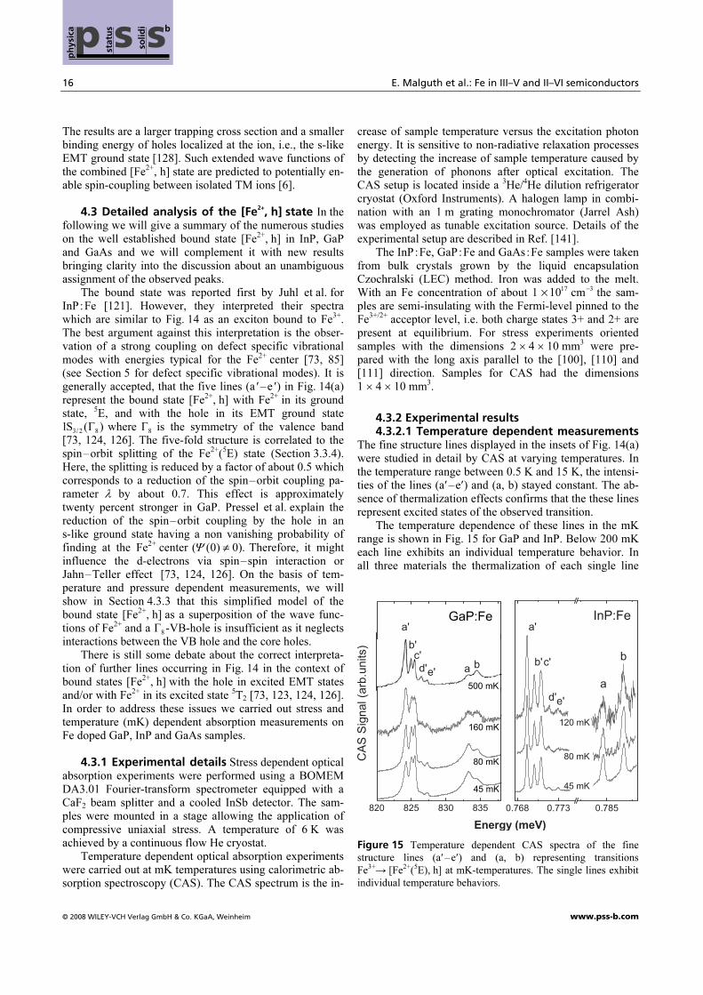
4.3.2 Experimental results 4.3.2.1 Temperature dependent measurements
The fine structure lines displayed in the insets of Fig. 14(a) were studied in detail by CAS at varying temperatures. In the temperature range between 0.5 K and 15 K, the intensi-ties of the lines (a′–e′) and (a, b) stayed constant. The ab-sence of thermalization effects confirms that the these lines represent excited states of the observed transition. The temperature dependence of these lines in the mK range is shown in Fig. 15 for GaP and InP. Below 200 mK each line exhibits an individual temperature behavior. In all three materials the thermalization of each single line
Figure 15 Temperature dependent CAS spectra of the fine
structure lines (a′–e′) and (a, b) representing transitions
Fe3+→ [Fe2+(5E), h] at mK-temperatures. The single lines exhibit
individual temperature behaviors.

phys. stat. sol. (b) (2008) 17
www.pss-b.com © 2008 WILEY-VCH Verlag GmbH & Co. KGaA, Weinheim
Review
Article
Figure 16 Sketch of an absorption transition with a two-fold
split ground state and one excited state.
exhibits a similar behavior which is the most pronounced for GaP. The temperature dependent behavior in the mK range must be the result of thermalization effects in the ground state. At mK temperatures the thermal activation energy is only a few µeV. Hence, the splitting of the ground state is much smaller than the linewidth (~1 meV). Consequently, each line represents a superposition of transitions with a common final state but individual ground states separated by a few µeV. In order to gain insights we assume a simple model outlined in Fig. 16. The ground state is split by DE into two levels with degeneracies
1g and
2,g respectively.
The population ratio 2 1/N N of the two sub-levels is given
by Boltzmann-statistic.
2 1
1 2
e .
E
kTN g
N g
D-
= (9)
If the respective oscillator strengths of the transitions are
1if and
2,i
f then the intensity of one absorption line as a function of temperature is given by
1 2 2
2 1 1
1
1 e ,
1 e
E
kT
E
kT
i i
i
i
Af f gI
g f g
g
D
D
Ê ˆ-Á ˜
Á ˜Á ˜- Ë ¯
= +
+
(10)
Table 8 Parameters of Eq. (10) determined by fitting the tem-
perature dependencies of lines (a′–e′) and (a, b) in Fig. 17.
a′ b′ c′ >d′ e′ >a b
GaP:Fe
∆E (µeV) 14.5 14.5 14.5 >14.5 14.5 >14.5 14.5
2 1g g/ 2 2 2 >2 2 >2 2
2 1i if f/ 1.6 0.8 0.5 >40 3 >0.2 2.7
A1if 3.5 3.2 4.2 <0.03 0.3 >2.2 0.6
InP:Fe
∆E (µeV) 8.5 8.5 8.5 >8.5 8.5 >8.5 8.5
2 1g g/ 2 2 2 >2 2 >2 2
2 1i if f/ 1.52 0.8 0.5 >9.2 2.3 <0.02 2
A1if 1.7 1.04 1.55 >0.04 0.1 >0.23 0.17
Figure 17 Temperature dependance of the seven fine structure
lines (a′–e′) and (a, b) observed in semi-insulating GaP and InP
(Fig. 15). The solid curves represent fits using Eq. (10) and the
parameters compiled in Table 8.
where A is a constant describing the intensity at T = 0 K. From Eq. (10) it can easily be seen that the temperature behavior depends on the ratio
2 1.
i if f/ This and other pa-
rameters, particularly ,ED can be determined by fitting the results from temperature dependent experiments according to Eq. (10). The results for GaP and InP are displayed in Fig. 17 and the used parameters are summarized in Table 8. A simultaneous fit of all seven lines is possible only for a degeneracy ratio of
2 12.g g/ = The determined ground state
splittings of 15 ± 3 µeV and 8 ± 2 µeV for GaP and InP, respectively, are in good agreement with ESR data for the splitting of the Fe3+(6A1) ground state (see Table 2, Sec-tion 3.2.1). No absolute values of the oscillator strengths can be given since the exact Fe3+ concentration of our samples is unknown.
4.3.2.2 Uniaxial stress experiments Uniaxial stress experiments were performed to obtain information on the electronic character of the bound states behind lines displayed in Fig. 14. Under uniaxial pressure along the [100]-, [110]- or [111]-axis, the crystal symmetry for Fe on cation site is reduced from
dT to
2dD ,
2vC or
3vC , respec-
tively. If the bound state can be described by a superposi-tion of a hole and an Fe2+ center, then the total stress in-duced splitting should equal the splitting of the Fe2+ states times the splitting of the
8Γ -VB-hole state. The splitting of
the Fe2+ states 5E and 5T2 under uniaxial pressure is pre-sented in Section 3.3.7. The fourfold degenerate
8Γ state of
the valence band hole splits into two twofold degenerate levels under stress in any direction. Consequently, twofold and fourfold splittings are expected. Figure 18 shows exemplary stress dependent absorp-tion spectra of the lines (a′–e′) for different uniaxial stress conditions. Small absorption coefficients and reduced intensities through splitting made the stress dependent measurements difficult to perform and it cannot be ruled out that very weak lines were not detected. While detailed

18 E. Malguth et al.: Fe in III–V and II–VI semiconductors
© 2008 WILEY-VCH Verlag GmbH & Co. KGaA, Weinheim www.pss-b.com
ph
ysic
ap s sstat
us
solid
i b
ENERGY (meV)
GaP:FeInP:FeT = 6 KT = 6 K
P || [111]P || [110]
34 MPa
0 MPa
820775770765 830825
x 0.5
69 MPa
114 MPa
148 MPa100 MPa
74 MPa
47 MPa
20 MPa
0 MPa x 0.5
Absorption(arb.units)
Figure 18 Exemplary absorption spectra of the quintet (a′–e′) in
GaP and InP under different uniaxial pressure conditions.
spectra could be recorded for the lines (a′–e′) in InP and GaP, the split lines (a, b) could be resolved only for InP. No distinct polarization of the split lines was observed con-firming that each line is a superposition of two lines origi-nating from the fine structure splitting of the Fe3+(6A1) ground state. The complete observed stress behavior of the lines (a′–e′) in InP and GaP is illustrated in Fig. 19 and is very similar for the two materials. Threefold splittings (e.g. line a′, P � [100]) and line shifts (e.g. line b, P � [100]) are in considerable disagreement with the simple model of a su-perposition outlined above. The stress-induced splitting of the lines a, b, A and A
1
in InP is shown in Fig. 20. In the following, the observed splitting is compared to the expected one outlined above.
820
822
824
826
828
830
766
768
770
772
774
776
0 50 100 150 0 50 100 150 0 50 100 150 200
Uniaxial Stress (MPa)
GaP:Fe
(a´-e´)
Energy(meV)
(a´-e´)
InP:Fe
P || [100] P || [110] P || [111]
Figure 19 Pressure-behavior of the quintet (a′–e′).
P � [111]: The lines a and b exhibit a twofold splitting of equal amplitude (9.5 meV/GPa) which can be attributed to the splitting of the hole, as the splitting of the
4Γ (5E) state
is too small to be resolved (see Section 3.3.7). P � [110]: Both lines a and b exhibit the expected behavior, a splitting of 10.0 meV/GPa on account of the hole (lines a, b) and a splitting of 6 meV/GPa of the Fe2+(
4Γ (5E)) state (line b).
The latter value is in good agreement with the splitting of 7 meV/GPa obtained from intra-center luminescence [87]. P � [100]: Although a splitting similar to P � [110] is ex-pected, here, only a twofold splitting is detected for line b
and none for line a. Further splitting may have been out-shone by the noisy background. For the interpretation of
Figure 20 Stress behavior of lines a, b, A, A1 in InP. In the top row, the magnitude of the stress induced splitting p
ED is displayed.

phys. stat. sol. (b) (2008) 19
www.pss-b.com © 2008 WILEY-VCH Verlag GmbH & Co. KGaA, Weinheim
Review
Article
the lines A and A1 the splitting of the Fe2+(
5Γ (5T2)) state
under stress has to be taken into account. For any direction a twofold splitting was established (Section 3.3.7). There-fore, a fourfold splitting is expected. However, only the twofold hole splitting is observed (Fig. 20). Concerning a quantitative analysis of the stress behav-ior of lines a, b, A and A
1, the splitting of the valance band
hole state under stress P is described by deformation po-tentials β and δ [143]. The splitting
hED of the free hole
state 8
Γ is given by:
h 11 12[100] 2 ( ) ,P E S S Pβ� : D = / (11)
1
22 2 2 2
h 11 12 44[110] [ ( ) ] ,P E S S S Pβ δ� : D = / + (12)
h 44
1[111] ,
3P E S Pδ�
Ê ˆ: D = Ë ¯ (13)
where ijS are elastic modules. For InP their values are: 2 1
111 65 10 GPa ,S
- -
= . ¥ 2 1
120 59 10 GPaS
- -
= - . ¥ and 2 1
42 17 10 GPaS
- -
= . ¥ [144]. The deformation potentials β and δ can be determined from the experimental data. The observed energetic splitting
pED is depicted in the top
row of Fig. 20. For the lines a and b it can be successfully fitted for all three directions with the values β ¢ = 0.245 eV and δ ¢ = 0.76 eV. Lines A and A
1 show slight deviations
from those fits indicating that the coupling between the hole and Fe2+ is different for the ground and excited state of Fe2+. Compared to the deformation potentials of the free exciton in InP (β = 1.55 eV, δ = 4.2 eV) [145], the values of the bound hole are reduced by the factor β β δ δ/ ª / ª¢ ¢ 0.17. Such a reduction of the deformation potentials is common for bound states [146]. The results of the stress dependent experiments can be summarized as follows: While the stress behavior of the lines a, b, A and A1 is in reasonable agreement with a su-perposition of hole and Fe2+, the one of the lines (a′–e′) is not. Hence, a more sophisticated model is required to de-scribe the bound state.
4.3.3. Discussion 4.3.3.1 The ground state The temperature depend-ence of the intensity of the absorption lines (a′–e′) and (a, b) in the mK range can be explained assuming a ground state consisting of two sub-levels. The found distance be-tween them amounts to 15 ± 3 µeV and 8 ± 2 µeV for GaP and InP, respectively, which is in good agreement with the splitting of the Fe3+(6A1) state determined by ESR (see Ta-ble 2, Section 3.2.1). The Fe3+ (6A1) state is split by sec-ond-order spin–orbit and spin–spin interaction into two levels of
7Γ and
8Γ symmetry separated by 3E aD = (a is
the fine structure parameter). The correct order cannot be obtained from ESR though. The
7Γ state is twofold and the
8Γ state fourfold degenerate. Hence, the found ratio of de-generacies g2/g1 = 2 leads to the conclusion that the
8Γ
level is located above the 7
Γ level.
4.3.3.2 The bound state [Fe2+(5E), h] In this section the bound state [Fe2+(5E), h] will be discussed which is the final state of the transitions represented by lines (a′–e′) and (a, b). First we will focus on the lines a and b. In agreement with previous works [121, 124], the lines a and b in InP are assigned to the formation of a bound state [Fe2+(5E), h] with the hole in its first excited EMT state,
3 2 82P (Γ )
/ and the Fe2+ center in the states 5
1Γ ( E) and
5
4Γ ( E), respectively. Key arguments are the small linewidth and the energy spacing equal to the spin–orbit splitting of the Fe2+(5E) state (Section 3.3.4). The stress behavior of the lines (a, b) is compliant with a superposi-tion of Fe2+ and a
8Γ -VB-hole supporting the interpretation
as a weakly bound and thus excited hole. For the following reasons we interpret the lines (a, b) in GaP the same way as in InP despite missing stress ex-periments for GaP and contrary assignment in previous works as TA phonons of the lines (a′–e′) [73]: (i) The lines are too narrow to be TA phonon replica. (ii) No analogous phonon structure is found in InP although other phonon satellites of lines (a′–e′) are quite similar in both materials. (iii) The lines (a, b) show the same temperature depend-ence in both materials. (iv) The temperature behavior of lines (a, b) is contrary to that of lines (a′, b′). The associa-tion of lines (a, b) in GaP with TA phonons is based on a complex model including a Jahn–Teller effect [73]. How-ever, a significant impact of a Jahn–Teller effect is rather unlikely given the weak phonon coupling of the complex. Moreover, the assignment of the weak resonances around 846 meV to be the analogue to the lines (a, b) in GaP does not comply with an over-all model of EMT states. This will be discussed below. Concerning lines (a′–e′), the model of a superposition of a
8Γ hole in the VB and the Fe2+(5E) center is not capa-
ble to explain the stress behavior of these lines. Also the inverse temperature dependence of lines (a′, b′) in com-parison with lines (a, b) necessitates a revised and more comprehensive model of the bound complex that also holds for the interpretation of lines a, b, A and A
1.
The quintet (a′–e′) can be explained conclusively by the model of a modified spin–orbit interaction (Sec-tion 4.3). However, the fundamentals of the formation of the [Fe2+, h] complex are not taken into account in this model. The interaction between the Fe2+ core and the hole is affected by spin–spin coupling and exchange interaction. The magnitude of these interactions scales with the overlap of the Fe2+ and hole wave functions. An evaluation of the magnitude of the exchange interaction is crucial as it repre-sents one of the major mechanisms of spin-coupling be-tween free carriers and TM centers (see above). The electronic structure of the [Fe2+(5E), h] bound states under the influence of exchange interaction is mod-eled in Fig. 21 for three different cases. If the exchange in-teraction is negligible compared to the spin–orbit interac-tion, then the fine structure of the bound state will be simi-lar to that of the unperturbed Fe2+(5E) state. In case of a weak exchange interaction that cannot be neglected, the re-

20 E. Malguth et al.: Fe in III–V and II–VI semiconductors
© 2008 WILEY-VCH Verlag GmbH & Co. KGaA, Weinheim www.pss-b.com
ph
ysic
ap s sstat
us
solid
i b
4
Figure 21 Symmetries and relative energies of [Fe2+(5E), h]
states under consideration of weak and strong exchange interac-
tion between the Fe2+(5E) spin–orbit states and the 8
Γ -VB-hole.
For a strong influence of the exchange interaction, only rough
predictions about the symmetries of the resulting states can be
made.
sulting splitting and symmetries can be acquired from the Kronecker-product of the Γ8-VB-hole and the Fe2+(5E) states. In case of a strong exchange interaction that is of the same order of magnitude as the spin–orbit coupling, the resulting states cannot be calculated from hole and Fe2+ states without major effort. In the latter case, a maxi-mum of thirteen states of
6Γ ,
7Γ and
8Γ symmetry are ex-
pected from group theory considerations. The observation of five equidistant lines suggests that the [Fe2+(5E), h] states are dominated by the fine structure of the Fe2+(5E) state ruling out effects of a strong exchange interaction. This leads us to the following comprehensive model explaining all experimental findings: (i) The pres-ence of the VB hole at the Fe2+ core leads to a reduced spin–orbit interaction (outlined above) and thus to a re-duced splitting of the Fe2+(5E) state. (ii) The impact of the exchange interaction between the VB hole and the Fe2+ core cannot be neglected and governs the symmetry of the resulting states. That leaves the determination of the symmetries of the five EMT ground states and a detailed comparison with the experimental results. The discussed transitions have initial states (Fe3+(6A1)) of
7Γ and
8Γ symmetry (Section 4.3.3).
Of possible transitions between 7
Γ and 8
Γ initial and 6
Γ ,
7Γ and
8Γ final states only the
7 7Γ Γ´ transition is for-
bidden. As a result of the Kronecker-product, lines a′ and e′ can easily be assigned to states of
8Γ symmetry. The in-
tensity of line d′ has a vanishing intensity at lowest tem-
peratures where only the Fe3+(7
Γ (6A1)) state is populated and rises quickly with increasing temperature where also the Fe3+(
8Γ (6A1)) state is populated thermally (Table 8,
Fig. 17). Consequently, the final state must be of 7
Γ sym-metry. Lines b′ and c′ must represent transitions into states of
6Γ or
8Γ symmetry since they are very pronounced even
at lowest temperatures (Table 8, Fig. 17). The stress behav-ior of the lines provide further clarity. From the appropri-ate multiplication table in Ref. [147] we see that for a re-duction of symmetry from
dT to
2vC ,
3vC or
2dD , a
8Γ state
splits into two or three levels whereas 6
Γ and 7
Γ states do not split but only change symmetry. A comparison with Fig. 19 delivers the symmetries of the lines (a′, b′, c′, d′, e′) to be
8(Γ ,
6Γ ,
8Γ ,
7Γ ,
8Γ ), respectively. The only experi-
mental result that remains unclear is the threefold splitting of line a′ under certain pressure conditions (Fig. 19). In order to determine the binding energy (
bE ) of the
bound state [Fe2+, h] a comparison with the EMT model is depicted in Fig. 22. The observed absorption lines are as-signed to EMT states by dashed lines. The EMT binding energies were taken from Ref. [127]. Line a was used as a reference because its final state was shown to be in good agreement with the first excited EMT state
3 22P .
/ Both the
spectra and the EMT axes were shifted so that the ioniza-tion thresholds (
bE = 0) of all materials line up with each
other. The experimentally found position of the ground state is shifted to higher energies (weaker bonding) as was pre-dicted by Fleurov [128]. While a shift of 3.9 meV and 3.2 meV for InP and GaAs, respectively, is relatively small, it is rather large for GaP (17.7 meV). The larger shift for GaP suggests a stronger localization of the ground state hole at the core. This assumption is supported by the larger reduction of the spin–orbit coupling in GaP discussed in the first part of Section 4.3. The stronger localization of the
3 2 81S (Γ )
/ hole at the Fe2+ core in GaP is also reflected by
the larger binding energy (stronger) predicted by EMT [127]. The weak resonances in the GaP spectrum labeled (
1a ,
1b ) represent the second excited EMT state,
3 2 82S (Γ ),
/
of the hole. Due to the s-type wavefunction this state is shifted to smaller binding energies (weaker) as well. This shift (6.7 meV) is not as large as that of the 1S state be-cause of the smaller probability of finding at the core. The binding energies of the [Fe2+, h] complex with the hole in the EMT ground state determined from the just outlined assignment are 31.3 meV for InP, 28.1 meV for GaP and 22.5 meV for GaAs. Unfortunately, the same effective-mass-like state in GaN could not be resolved as well as in GaP, InP and GaAs [12]. Furthermore, no EMT calculations as detailed as in Ref. [127] exist for acceptor impurities in GaN. For those two reasons, we can only attempt a tentative deter-mination of the binding energy in GaN. We calculate the binding energy using simplified EMT: 2 2
b*/( ),E Rm nε= -
with the Rydberg constant R= 13.6 eV, the relative effec-tive mass of the hole in GaN *m = 83 [148], effective di-

phys. stat. sol. (b) (2008) 21
www.pss-b.com © 2008 WILEY-VCH Verlag GmbH & Co. KGaA, Weinheim
Review
Article
Binding Energy (meV)
InP:Fe
GaP:Fe
GaAs:Fe
Absorption(arb.units)
-50 -40 -30 -20 -10 0 10
exp.
(a´- e´)
(a´- e´)
(a´- e´)
(a - d)
(a - d)
(a,b)(a ,b )1 1
exp.
exp.
EMT
EMT
EMT
1S ( )3/2 8Γ 2P ( )3/2 8Γ
2P ( )3/2 8Γ
2P ( )3/2 8Γ
2S ( )3/2 8Γ
1S ( )3/2 8Γ
1S ( )3/2 8Γ
Figure 22 Comparison and association of the fine structure lines
of the (Fe2+(5E), h) complex with EMT states. The EMT values
are taken from Ref. [127]. Line a was taken as a reference. The
lines (a–d) are in good agreement with the 3 2 8
2P (Γ )/
EMT state.
The binding energies of the s-type EMT states 3 2 8
1S (Γ )/
and
3 2 82S (Γ )
/ are shifted to higher energies (weaker bonding) because
of hybridization effects of the Fe2+ d-orbitals with the ligands.
The reduced spin–orbit splitting is caused by the presence of the
hole at the Fe2+ core partially quenching the spin–orbit coupling.
electric constant ε = 9.5 and the “main” quantum number n. We interpret the resonances 24 meV and 37 meV above the ground state at 2.812 eV [12] as the first (n = 2) and second excited (n = 3) EMT states, respectively. For n = 1, 2, 3, we receive
bE = 125, 31, 14 meV, respectively.
The difference between the last two values (17 meV) is larger than found experimentally (13 meV) which can be explained by the first excited shifting stronger to smaller binding energies. If we assume the second excited state to remain unshifted, we obtain a binding energy of the ground state of 51 meV. This result is in good agreement with the value of about 50 meV derived from the distance to the photoionization threshold [12]. Because of the coarse model applied above this new value cannot be considered more accurate. A binding energy of ≈50 meV means a shift of 75 meV according to our model. This is one order of magnitude larger than for GaP, InP and GaAs. This
could be explained by the relatively small lattice constant leading to a stronger hybridization of the Fe2+ d-orbitals with the VB [128]. 4.3.3.3 The bound state [Fe2+(5T2), h] In this sec-tion the bound state [Fe2+(5T2), h] will be discussed which is the final state of the transitions represented by lines (A, A
1, A
2), (C, C
1, C
2) and D in Fig. 14(b).
The lines A, C and D in InP and GaAs are assigned to the formation of [Fe2+(5T2), h] complexes with the hole in its first excited EMT state
3 2 82 (Γ )P
/ and the Fe2+ center in
the first three 5T2 states with reasonable transition prob-abilities, respectively. These 5T2 states are the result of the strong Jahn–Teller coupling on the 5T2 spin–orbit levels discussed in Section 3.3.5. The mentioned transition prob-ability is the one for transitions starting at the Fe3+(6A1) state. These are unknown since relative intensities have only been calculated for transitions starting at the Fe2+(5
1E(Γ )) state [78]. Thus, the only thing we can tell for
certain is that the Fe2+(5T2) state involved in the bound state behind the lines (A, A1, A2) is the
5Γ state which re-
mains unaffected by the Jahn–Teller effect (Section 3.3.5). The Fe2+(5T2) states involved in the lines (C, C
1, C
2) and D
are unclear. The above assignment is supported by the
GaAs:Fe
-20 -10 0
C
D
C1 C2
10 20
Binding Energy (meV)
Absorption(arb.units)
InP:Fe
GaP:Fe
continuum
A A1 A2
continuum
A1A A2
continuum
C1C C2
continuum
[Fe ( T ( )),h]2+ 5
2 5Γ
[Fe ( T ( )),h]2+ 5
2 JTΓ
[Fe ( T ( )),h]2+ 5
2 JTΓ
[Fe ( T ( )),h]2+ 5
2 5Γ
Figure 23 Assignment of the fine structure lines of the
(Fe2+(5T2), h) complex to EMT states of the hole. On the inserted
EMT axes, the positions of the first four excited states 3 2 8
2P (Γ ),/
3 2 82S (Γ ),
/
5 2 82P (Γ )
/ and
5 2 72P (Γ )
/ are indicated as well as the
ionization thresholds. The EMT ground state 3 2 8
2S (Γ )/
does not
appear in these spectra for reasons given in the text. The EMT
values are taken from Ref. [127].
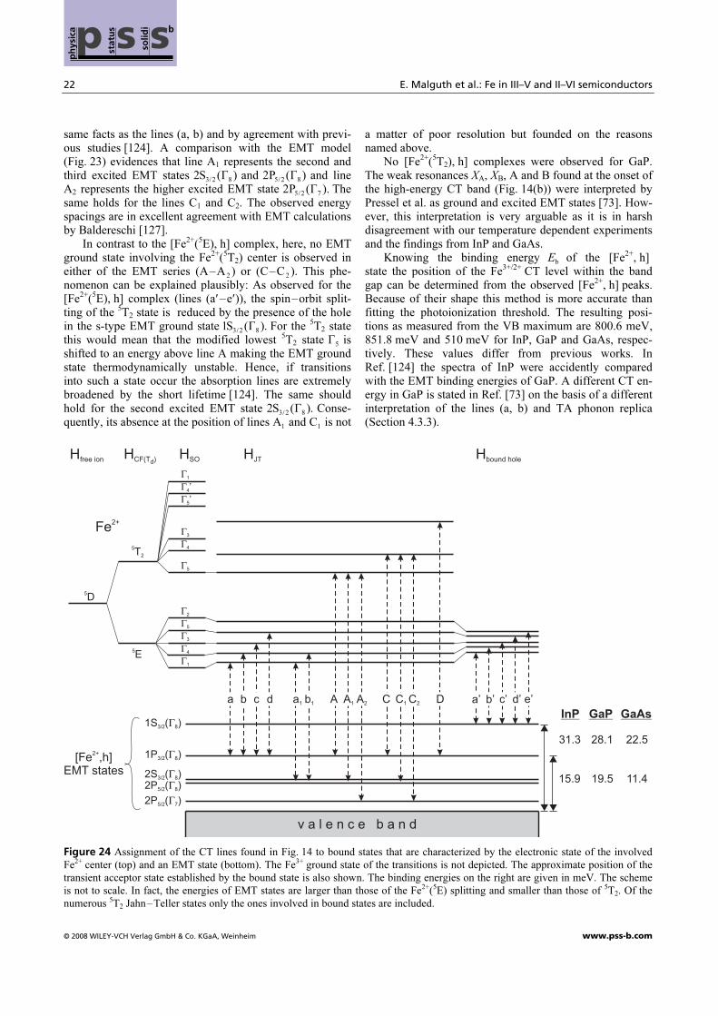
22 E. Malguth et al.: Fe in III–V and II–VI semiconductors
© 2008 WILEY-VCH Verlag GmbH & Co. KGaA, Weinheim www.pss-b.com
ph
ysic
ap s sstat
us
solid
i b
same facts as the lines (a, b) and by agreement with previ-ous studies [124]. A comparison with the EMT model (Fig. 23) evidences that line A1 represents the second and third excited EMT states
3 2 82S (Γ )
/ and
5 2 82P (Γ )
/ and line
A2 represents the higher excited EMT state 5 2 7
2P (Γ )./
The same holds for the lines C1 and C2. The observed energy spacings are in excellent agreement with EMT calculations by Baldereschi [127]. In contrast to the [Fe2+(5E), h] complex, here, no EMT ground state involving the Fe2+(5T2) center is observed in either of the EMT series (A–A
2) or (C–C
2). This phe-
nomenon can be explained plausibly: As observed for the [Fe2+(5E), h] complex (lines (a′–e′)), the spin–orbit split-ting of the 5T2 state is reduced by the presence of the hole in the s-type EMT ground state
3 2 81S (Γ ).
/ For the 5T2 state
this would mean that the modified lowest 5T2 state 5
Γ is shifted to an energy above line A making the EMT ground state thermodynamically unstable. Hence, if transitions into such a state occur the absorption lines are extremely broadened by the short lifetime [124]. The same should hold for the second excited EMT state
3 2 82S (Γ ).
/ Conse-
quently, its absence at the position of lines A1 and C
1 is not
a matter of poor resolution but founded on the reasons named above. No [Fe2+(5T2), h] complexes were observed for GaP. The weak resonances XA, XB, A and B found at the onset of the high-energy CT band (Fig. 14(b)) were interpreted by Pressel et al. as ground and excited EMT states [73]. How-ever, this interpretation is very arguable as it is in harsh disagreement with our temperature dependent experiments and the findings from InP and GaAs. Knowing the binding energy
bE of the [Fe2+, h]
state the position of the Fe3+/2+ CT level within the band gap can be determined from the observed [Fe2+, h] peaks. Because of their shape this method is more accurate than fitting the photoionization threshold. The resulting posi-tions as measured from the VB maximum are 800.6 meV, 851.8 meV and 510 meV for InP, GaP and GaAs, respec-tively. These values differ from previous works. In Ref. [124] the spectra of InP were accidently compared with the EMT binding energies of GaP. A different CT en-ergy in GaP is stated in Ref. [73] on the basis of a different interpretation of the lines (a, b) and TA phonon replica (Section 4.3.3).
Hfree ion HSO
5D
E5
5T2
Γ1
Γ4
Γ3
Γ5
Γ2
Γ1
Γ4
Γ3
Γ5
Γ5’
Γ4’
HCF(T )d
1S ( )3/2 8Γ
1P ( )3/2 8Γ
2S ( )3/2 8Γ2P ( )5/2 8Γ2P ( )5/2 7Γ
InP GaAsGaP
Hbound holeHJT
v a l e n c e b a n d
a b c d a1 b1 A1A A2 C1C C2 D e’b’ c’ d’a’
[Fe ,h]EMT states
2+
Fe2+
31.3 28.1 22.5
15.9 11.419.5
Figure 24 Assignment of the CT lines found in Fig. 14 to bound states that are characterized by the electronic state of the involved
Fe2+ center (top) and an EMT state (bottom). The Fe3+ ground state of the transitions is not depicted. The approximate position of the
transient acceptor state established by the bound state is also shown. The binding energies on the right are given in meV. The scheme
is not to scale. In fact, the energies of EMT states are larger than those of the Fe2+(5E) splitting and smaller than those of 5T2. Of the
numerous 5T2 Jahn–Teller states only the ones involved in bound states are included.

phys. stat. sol. (b) (2008) 23
www.pss-b.com © 2008 WILEY-VCH Verlag GmbH & Co. KGaA, Weinheim
Review
Article
If we want to estimate the extent of the EMT ground state [Fe2+, h] state we need to keep in mind that it does not comply exactly with EMT. However, assuming an effec-tive-mass-like state the effective radius can be sized up by
B b* ( *)a a R E ε= / from the found binding energy
bE
(in eV), with the Bohr radius B,a the Rydberg constant R
and the effective dielectric constant *.ε Values for the 3 2
1S/
state of 2.3 nm, 1.8 nm, 2.5 nm and 1.5 nm for GaP, InP, GaAs and GaN, respectively, indicate that the bound hole should still be characterized by VB properties. 4.3.4 Concluding remarks The bound states found in InP, GaP and GaAs are summarized in Fig. 24. The situation depicted in Fig. 24 should be similar in other ma-terials, particularly in GaN. Regarding carrier mediated spin-coupling, our findings yield the following implications. The various bound states [Fe2+ , h] depicted in Fig. 24 provide scores of shallow ac-ceptor levels. The at least weak exchange interaction within the s-type EMT states,
3 2 81S (Γ )
/ and
3 2 82S (Γ ),
/
should facilitate spin-coupling between the hole and the Fe2+ center. From the determined extent of the bound state, *a ≈ 2 nm, the critical Fe concentration
c,N for which an
overlap of the wave functions enables a long-range inter- action, can be calculated from the Mott criterion
3
c(0 25 *)N aª . / ª 2
1810¥ cm 3
.
- At room temperature, the first excited EMT state should be occupied with an at least four times larger radius potentially enabling extended in-teractions already at smaller concentrations. At even lower Fe densities, carrier mediated spin-coupling could be es-tablished via holes being captured and thermally released by the Fe centers [136]. This coupling mechanism is sup-ported by the relatively small binding energy of the magni-tude equal to the thermal energy at room temperature. However, it needs to be kept in mind that the relaxation of the bound state into Fe3+ represents a competing process. Unfortunately, the lifetime of this process is still unknown. 5 Fe-specific vibrational modes The different mass of an impurity atom in comparison to the cation it is re-placing leads to a change of local vibrational modes. Re-sulting defect specific vibrational modes have been re-ported for Fe in GaP, GaAs, InP, GaN, ZnO [12, 46, 72, 84, 85, 149–152]. In General, different charge states and even different electronic states of the same charge state exhibit individual defect specific modes because each electronic configuration results in a different coupling constant in the model of the harmonic oscillator [84, 85]. Such defect specific vibrational modes can be observed by means of Raman spectroscopy or in the form of replica of defect related luminescence or absorption lines. For both methods caution needs to be taken when interpreting new lines arising upon impurity introduction. The presence of a point defect may cause silent lattice modes to become allowed by breaking the translational symmetry of the bulk crystal [153]. Further care needs to be taken when assigning replica of internal transitions. As demonstrated
in Section 3.3, alleged replica on account of defect specific vibrational modes may in fact arise from transitions involving vibrational states affected by Jahn–Teller coupling [78]. In order to avoid misinterpretation experi-mental findings should be compared with theoretical calcu-lations. Concerning GaP, InP and GaAs, Pressel and coworkers distinguish three different kinds defect specific vibrational modes [46, 72, 84, 85]: Resonant modes (RM) are degen-erate with lattice phonon states. Gap modes (GM) are lo-cated within the phonon band gap and are characteristic for phosphorous ligands. Local modes (LM) have larger ener-gies than optical lattice phonons. For exact energies of Fe specific vibrational modes in GaP, GaAs, InP, GaN see Refs. [12, 72, 84, 85]. A comparison of these works with theoretical calculations [78, 151] confirms the identity of the found modes. 6 Summary For the realization of spin-coupling in a DMS a detailed quantitative understanding of the elec-tronic states introduced through TM doping is essential. The electronic properties of Fe doped III–V and II–VI compound semiconductors were reviewed and the involved experimental methods were presented. The Fe3 2+/ + level is found within the band gap of many materials while the Fe2 1+/ + level has only been observed in a few and the Fe3 4+/ + level in none. While the position of the CT levels has mainly been derived from the photoioni-zation threshold, it can be determined with higher accuracy via the effective-mass-like state [Fe2+, h]. To date no CT level has been detected in ZnO. On the basis of trends of the position of the CT levels within related material sys-tems (internal reference rule), predictions about as yet un-detected CT levels could be made. The results were dis-cussed against the background of a potential realization of a ferromagnetic coupling in DMS’s. The suitability of Fe doped GaN for hole-mediated spin-couping critically de-pends on whether the Fe3 4+/ + donor level is found above or below the VB edge. The deep Fe2 3+/ + donor level in II–VI compounds renders these materials unsuitable for hole me-diated spin-coupling. Detailed term schemes of the Fe ions in tetrahedral and trigonal crystal field symmetry are presented, includ-ing hyperfine structure, isotope effects and Jahn–Teller effect. Most of the insights about the respective electronic structure was obtained from the radiative transitions Fe3+(4T1 → 6A1) and Fe2+(5E → 5T2). The trigonal symme-try in hexagonal crystals can be approximated by a pertur-bation in the form of an axial distortion of the tetrahedral case. While a weak or intermediate Jahn–Teller coupling was shown to effect most Fe electronic states, the fine structure of the Fe2+(5T2) state is significantly altered by a strong Jahn–Teller effect. From the established term-schemes in combination with the positions of the CT levels, we concluded that, except for the effective-mass-like state, no levels close to one of the bands are formed by the Fe impurity.

24 E. Malguth et al.: Fe in III–V and II–VI semiconductors
© 2008 WILEY-VCH Verlag GmbH & Co. KGaA, Weinheim www.pss-b.com
ph
ysic
ap s sstat
us
solid
i b
The collected data indicate small but non-negligible degrees of covalency between Fe and the ligands. It scales with the degree of covalency of the host crystal. New insights on the shallow effective-mass-like accep-tor state [Fe2+, h] could be obtained by means of tempera-ture dependent CAS experiments in the mK range as well as stress dependent measurements. The binding energy and effective Bohr radius were determined for GaN, GaP, InP and GaAs and a weak exchange interaction between the hole and the Fe2+center was detected. Our results also provide insights into the hyperfine structure of the Fe3+ ground state, 6A1: In GaP and InP, the
8Γ level is found above the
7Γ level.
Acknowledgement We thank Lars Podlowski and Torsten
Wolf for carrying out the CAS experiments.
References
[1] R. P. Vaudo, X. Xu, A. Salant, J. Malcarne, and G. R. Bran-
des, phys. stat. sol. (a) 200(1), 18–21 (2003).
[2] S. A. Wolf, D. D. Awschalom, R. A. Buhrman, J. M.
Daughton, S. von Molnar, M. L. Roukes, A. Y. Chtchelka-
nova, and D. M. Treger, Science 294(5546), 1488–1495
(2001).
[3] T. Dietl, H. Ohno, F. Matsukura, J. Cibert, and D. Ferrand,
Science 287(5455), 1019–1022 (2000).
[4] T. Jungwirth, J. Sinova, J. Masek, J. Kucera, and A. H.
MacDonald, Rev. Mod. Phys. 78(3), 809 (2006).
[5] H. Ohno, Science 281(5379), 951–956 (1998).
[6] T. Dietl, H. Ohno, and F. Matsukura, Phys. Rev. B 63(19),
195205 (2001).
[7] T. Dietl, phys. stat. sol. (b) 240(2), 433–439 (2003).
[8] T. Graf, S. T. B. Goennenwein, and M. S. Brandt, phys. stat.
sol. (b) 239(2), 277–290 (2003).
[9] A. Bonanni, Semicond. Sci. Technol. 22(9), R41–R56
(2007).
[10] C. Zener, Phys. Rev. 82(3), 403 – 405 (1951).
[11] T. Dietl, F. Matsukura, and H. Ohno, Phys. Rev. B 66(3),
033203 (2002).
[12] E. Malguth, A. Hoffmann, W. Gehlhoff, O. Gelhausen, M. R.
Phillips, and X. Xu, Phys. Rev. B 74(16), 165202 (2006).
[13] J. M. Langer and H. Heinrich, Phys. Rev. Lett. 55, 1414
(1985).
[14] J. M. Langer, C. Delerue, M. Lannoo, and H. Heinrich,
Phys. Rev. B 38, 7723 (1988).
[15] I. Vurgaftman, J. R. Meyer, and L. R. Ram-Mohan, J. Appl.
Phys. 89(11), 5815–5875 (2001).
[16] S. H. Wei and A. Zunger, Appl. Phys. Lett. 72(16), 2011–
2013 (1998).
[17] P. Rinke, M. Scheffler, A. Qteish, M. Winkelnkemper,
D. Bimberg, and J. Neugebauer, Appl. Phys. Lett. 89(16),
161919 (2006).
[18] K. M. Yu, Z. Liliental-Weber, W. Walukiewicz, W. Shan,
J. W. Ager, III, S. X. Li, R. E. Jones, E. E. Haller, H. Lu,
and W. J. Schaff, Appl. Phys. Lett. 86(7), 071910 (2005).
[19] B. K. Ridley, J. Phys. C, Solid State Phys. 13(10), 2015–
2026 (1980).
[20] B. K. Ridley and M. A. Amato, J. Phys. C, Solid State Phys.
14(9), 1255–1269 (1981).
[21] M. A. Amato and B. K. Ridley, J. Phys. C, Solid State Phys.
13(10), 2027–2040 (1980).
[22] W. C. Holton, J. Schneider, and T. L. Estle, Phys. Rev.
133(6A), A1638–A1641 (1964).
[23] A. Zunger, Solid State Phys. 39, 275 (1986).
[24] J. M. Baranowski, in: Deep Centers in Semiconductors, ed-
ited by S. T. Pantelides (Gordon and Breach, New York,
1986), p. 691.
[25] R. Heitz, A. Hoffmann, and I. Broser, Phys. Rev. B 45(16),
8977–8988 (1992).
[26] S. Brehme, J. Phys. C, Solid State Phys. 18(13), L319–L323
(1985).
[27] J. Baur, K. Maier, M. Kunzer, U. Kaufmann, and J. Schnei-
der, Appl. Phys. Lett. 65(17), 2211–2213 (1994).
[28] M. Godlewski and A. Zakrzewski, J. Phys. C, Solid State
Phys. 18(36), 6615–6625 (1985).
[29] H. Zimmermann, R. Boyn, and N. Nagel, phys. stat. sol. (b)
117(1), 229–239 (1983).
[30] H. Lechner, D. M. Hofmann, B. K. Meyer, M. Azoulay,
K. Krambrock, J. M. Spaeth, A. Dörnen, B. Kaufmann,
M. S. P. Omling, and K. W. Benz, Adv. Mater. Opt. Elec-
tron. 3(1–6), 223–232 (1994).
[31] W. Jantsch and G. Hendorfer, J. Cryst. Growth 101(1–4),
404–413 (1990).
[32] A. J. Szadkowski, J. Phys.: Condens. Matter 2(49), 9853–
9859 (1990).
[33] J. Dieleman, J. W. de Jong, and T. Meijer, J. Chem. Phys.
45(9), 3178–3184 (1966).
[34] B. V. Shanabrook, P. B. Klein, and S. G. Bishop, Physica B
116, 444 (1983).
[35] We observed the Fe2+ 5 5
2( E T )Æ transition in ZnO by Fou-
rier transform infrared transmission spectroscopy at
395 meV (to be published).
[36] U. Gerstmann, A. T. Blumenau, and H. Overhof, Phys. Rev.
B 63(7), 075204 (2001).
[37] M. Wegscheider, C. Simbrunner, H. Przybylinska, M. Kie-
cana, M. Sawicki, A. Navarro-Quezada, H. Sitter, W. Jantsch,
T. Dietl, and A. Bonanni, phys. stat. sol. (a) 204(1), 86–91
(2007).
[38] K. Sato and H. Katayama-Yoshida, Jpn. J. Appl. Phys.
40(5B), L485–L487 (2001).
[39] M. Herbich, A. Twardowski, D. Scalbert, and A. Petrou,
Phys. Rev. B 58(11), 7024–7034 (1998).
[40] U. Kaufmann and J. Schneider, Festkörperprobleme: Ad-
vances in Solid State Physics (Vieweg, Braunschweig,
1980), p. 87.
[41] K. Maier, M. Kunzer, U. Kaufmann, J. Schneider, B. Mo-
nemar, I. Akasaki, and H. Amano, Mater. Sci. Forum 143–
147, 93–97 (1994).
[42] W. Gehlhoff, D. Azamat, U. Haboeck, and A. Hoffmann,
Physica B 376/377, 486–490 (2006).
[43] H. A. Jahn and E. Teller, Proc. R. Soc. Lond. A, Math.
Phys. Sci. 161(905), 220 (1937).
[44] T. Buch, B. Clerjaud, B. Lambert, and P. Kovacs, Phys.
Rev. B 7(1), 184 – 191 (1973).
[45] A. Hoffmann, R. Heitz, and I. Broser, Phys. Rev. B 41(9),
5806–5816 (1990).
[46] K. Pressel, G. Bohnert, A. Dörnen, B. Kaufmann, J. Den-
zel, and K. Thonke, Phys. Rev. B 47(15), 9411–9417
(1993).

phys. stat. sol. (b) (2008) 25
www.pss-b.com © 2008 WILEY-VCH Verlag GmbH & Co. KGaA, Weinheim
Review
Article
[47] B. Kaufmann, A. Dörnen, and F. S. Ham, in: 23rd Interna-
tional Conference on the Physics of Semiconductors, Berlin
1996, Vol. 4, edited by M. Scheffler and R. Zimmermann
(World Scientific, Singapore, 1996), p. 2829.
[48] K. Pressel, G. Bohnert, G. Rückert, A. Dörnen, and K. Thon-
ke, J. Appl. Phys. 71(11), 5703–5705 (1992).
[49] R. Heitz, P. Thurian, I. Loa, L. Eckey, A. Hoffmann, I. Bro-
ser, K. Pressel, B. K. Meyer, and E. N. Mokhov, Appl. Phys.
Lett. 67(19), 2822–2824 (1995).
[50] J. Baur, K. Maier, M. Kunzer, U. Kaufmann, J. Schneider,
H. Amano, I. Akasaki, T. Detchprohm, and K. Hiramatsu,
Appl. Phys. Lett. 64(7), 857–859 (1994).
[51] D. Boulanger, D. Curie, and R. Parrot, J. Lumin. 48/49,
680–684 (1991).
[52] W. A. Harrison, Phys. Rev. B 8(10), 4487 (1973).
[53] C. K. Jørgensen, Discuss. Faraday Soc. 26, 110–115
(1958).
[54] P. Thurian, A. Hoffmann, L. Eckey, P. Maxim, R. Heitz,
I. Broser, K. Pressel, B. K. Meyer, J. Schneider, J. Bauer,
and M. Kunzer, in: III–V Nitrides, Symposium, Boston
1996, edited by F. Ponce, T. Moustakas, I. Akasaki, and
B. Monemar (Mater. Res. Soc., 1997), p. 707.
[55] W. C. Holton, M. de Wit, T. L. Estle, B. Dischler, and
J. Schneider, Phys. Rev. 169(2), 359–372 (1968).
[56] B. Bleaney and R. S. Trenam, Proc. R. Soc. Lond. A 223
(April), 1–14 (1954).
[57] A. Räuber and J. Schneider, Z. Naturforsch. A 17, 266–270
(1962).
[58] J. Schneider, Z. Naturforsch. A 17, 189 (1962).
[59] W. M. Walsh and L. W. Rupp, Phys. Rev. 126(3), 952–955
(1962).
[60] W. Teuerle, E. Blaschke, and A. Hausmann, Z. Phys. A
270(1), 37–41 (1974).
[61] M. de Wit and T. L. Estle, Phys. Rev. 132(1), 195–201
(1963).
[62] G. H. Stauss, J. J. Krebs, and R. L. Henry, Phys. Rev. B
16(3), 974 (1977).
[63] T. L. Estle, Phys. Rev. 136(6A), A1702–A1704 (1964).
[64] J. C. Hensel, Bull. Am. Phys. Soc. 9, 244 (1964).
[65] J. Lambe, J. Baker, and C. Kikuchi, Phys. Rev. Lett. 3(6),
270–271 (1959).
[66] G. Brunthaler, U. Kaufmann, and J. Schneider, J. Appl.
Phys. 56(10), 2974–2976 (1984).
[67] R. S. Title, Phys. Rev. 131(2), 623–627 (1963).
[68] P. Koidl, phys. stat. sol. (b) 74(2), 477–484 (1976).
[69] R. Heitz, P. Maxim, L. Eckey, P. Thurian, A. Hoffmann,
I. Broser, K. Pressel, and B. K. Meyer, Phys. Rev. B 55(7),
4382–4387 (1997).
[70] U. W. Pohl, A. Ostermeier, W. Busse, and H. E. Gumlich,
Phys. Rev. B 42(9), 5751–5758 (1990).
[71] R. Parrot, A. Geoffroy, C. Naud, W. Busse, and H. E. Gum-
lich, Phys. Rev. B 23(10), 5288–5300 (1981).
[72] K. Pressel, G. Rückert, A. Dörnen, and K. Thonke, Phys.
Rev. B 46(20), 13171–13178 (1992).
[73] K. Pressel, A. Dörnen, G. Rückert, and K. Thonke, Phys.
Rev. B 47(24), 16267–16273 (1993).
[74] E. Malguth, A. Hoffmann, M. Phillips, and W. Gehlhoff,
Mater. Res. Soc. Symp. Proc. 892, 131–136 (2006).
[75] E. E. Vogel, O. Mualin, M. A. de Orúe, and J. Rivera-
Iratchet, Phys. Rev. B 44(4), 1579–1587 (1991).
[76] E. E. Vogel, O. Mualin, M. A. de Orúe, J. Rivera-Iratchet,
M. L. Flores, U. W. Pohl, H. J. Schulz, and M. Thiede,
Phys. Rev. B 50(8), 5231 (1994).
[77] H. J. Schulz, M. Thiede, U. W. Pohl, J. Rivera-Iratchet,
M. A. de Orúe, M. L. Flores, O. Mualin, and E. E. Vogel,
Z. Phys. B, Condens. Matter 98(2), 215–221 (1995).
[78] O. Mualin, E. E. Vogel, M. A. de Orúe, L. Martinelli,
G. Bevilacqua, and H. J. Schulz, Phys. Rev. B 65(3),
035211 (2001).
[79] W. Low and M. Weger, Phys. Rev. 118(5), 1119–1130
(1960).
[80] G. A. Slack, F. S. Ham, and R. M. Chrenko, Phys. Rev. B
152(1), 376–402 (1966).
[81] F. S. Ham and G. A. Slack, Phys. Rev. B 4(3), 777–798
(1971).
[82] G. A. Slack and B. M. O’Meara, Phys. Rev. 163(2), 335
(1967).
[83] E. Malguth, A. Hoffmann, and X. Xu, Phys. Rev. B 74(16),
165201 (2006).
[84] G. Rückert, K. Pressel, A. Dörnen, K. Thonke, and W. Ul-
rici, Phys. Rev. B 46(20), 13207–13214 (1992).
[85] K. Pressel, K. Thonke, A. Dörnen, and G. Pensl, Phys.
Rev. B 43(3), 2239 (1991).
[86] W. H. Koschel, U. Kaufmann, and S. G. Bishop, Solid
State Commun. 21(12), 1069–1072 (1977).
[87] K. Thonke, K. Pressel, H. U. Hermann, and A. Dörnen,
Mater. Sci. Forum 38–41, 869–873 (1989).
[88] J. M. Baranowski, J. W. Allen, and G. L. Pearson, Phys.
Rev. 160(3), 627–692 (1967).
[89] J. H. Haanstra, in: International Conference on II–VI
Semiconductor Compounds, edited by D. G. Thomas
(W. A. Benjamin, New York, 1967), pp. 207–214.
[90] G. Roussos, H. J. Schulz, and M. Thiede, J. Lumin. 31/32
(Part 1), 409–411 (1984).
[91] D. Buhmann, H. J. Schulz, and M. Thiede, Phys. Rev. B
24(11), 6221–6233 (1981).
[92] K. Pressel, Ph.D. thesis, Universität Stuttgart (1985).
[93] M. V. Klein, in: Light Scattering in Solids I, edited by
M. Cardona (Springer, Berlin, 1975), p. 179.
[94] G. Goetz and H. J. Schulz, J. Lumin. 40/41, 415–416
(1988).
[95] G. A. Slack, S. Roberts, and F. S. Ham, Phys. Rev. 155(2),
170–177 (1967).
[96] M. Skowronski and Z. Liro, J. Phys. C, Solid State Phys.
15(1), 137–145 (1982).
[97] S. A. Kazanskii, A. I. Ryskin, and G. I. Khil’ko, Opt.
Spektrosk. 27(2), 296 (1969).
[98] M. K. Udo, M. Villeret, I. Miotkowski, A. J. Mayur, A. K.
Ramdas, and S. Rodriguez, Phys. Rev. B 46(12), 7459–
7468 (1992).
[99] K. Pressel, K. Thonke, and A. Dörnen, in: 20th Int.
Conf. Phys. Semic., Thessaloniki 1990, Vol. 1, edited by
E. M. Anastassakis and J. D. Joannopoulos (World Scien-
tific, Singapore, 1990), p. 690.
[100] L. Podlowski, R. Heitz, P. Thurian, A. Hoffmann, and
I. Broser, J. Lumin. 48, 252–256 (1994).
[101] C. Testelin, C. Rigaux, A. Mauger, A. Mycielski, and
C. Julien, Phys. Rev. B 46(4), 2183–2192 (1992).
[102] J. T. Vallin, G. A. Slack, and C. C. Bradley, Phys. Rev. B
2(11), 4406–4413 (1970).

26 E. Malguth et al.: Fe in III–V and II–VI semiconductors
© 2008 WILEY-VCH Verlag GmbH & Co. KGaA, Weinheim www.pss-b.com
ph
ysic
ap s sstat
us
solid
i b
[103] C. L. West, W. Hayes, J. F. Ryan, and P. J. Dean, J. Phys.
C, Solid State Phys. 13(30), 5631–5643 (1980).
[104] M. Villeret, S. Rodriguez, and E. Kartheuser, Phys. Rev. B
43(4), 3443–3449 (1991).
[105] S. W. Biernacki, phys. stat. sol. (b) 102(1), 235 (1980).
[106] L. Martinelli, G. Bevilacqua, J. Rivera-Iratchet, M. A. de
Orúe, O. Mualin, E. E. Vogel, and J. Cartes, Phys. Rev. B
62(16), 10873–10881.
[107] J. Rivera-Iratchet, M. A. de Orúe, and E. E. Vogel, Phys.
Rev. B 34(6), 3992 (1986).
[108] M. A. de Orúe, J. Rivera-Iratchet, and E. E. Vogel, J.
Cryst. Growth 86(1–4), 28–32 (1990).
[109] E. E. Vogel, J. Rivera-Iratchet, and M. A. de Orúe, Phys.
Rev. B 38(5), 3556 (1988).
[110] J. Rivera-Iratchet, M. A. de Orúe, M. L. Flores, and E. E.
Vogel, Phys. Rev. B 47(16), 10164 (1993).
[111] L. Martinelli, G. Bevilacqua, E. E. Vogel, and O. Mualin,
Phys. Rev. B 65(15), 155203 (2002).
[112] E. E. Vogel, O. Mualin, H. J. Schulz, and M. Thiede,
Z. Phys. Chem. 201(1–2), 99–109 (1997).
[113] M. Villeret, S. Rodriguez, and E. Kartheuser, J. Appl.
Phys. 67(9), 4221–4232 (1990).
[114] E. E. Vogel, M. A. de Orúe, J. Rivera-Iratchet, and J. E.
Morales, J. Cryst. Growth 101(1–4), 470–473 (1990).
[115] A. Karipidou, H. Nelkowski, and G. Roussos, J. Cryst.
Growth 59(1–2), 307–311 (1982).
[116] H. Nelkowski, O. Pfutzenreuter, and W. Schrittenlacher,
J. Lumin. 17(4), 419–423 (1978).
[117] K. P. O’Donnell, K. M. Lee, and G. D. Watkins, J. Phys. C,
Solid State Phys. 16(20), L723–L728 (1983).
[118] U. Kaufmann and J. Schneider, Solid State Commun.
21(12), 1073–1075 (1977).
[119] T. L. Estle and W. C. Holton, Phys. Rev. 150(1), 159–167
(1966).
[120] R. Kernocker, K. Lischka, and L. Palmetshofer, J. Cryst.
Growth 86(1–4), 625–628 (1990).
[121] A. Juhl, A. Hoffmann, D. Bimberg, and H. J. Schulz,
Appl. Phys. Lett. 50(18), 1292–1294 (1987).
[122] A. H. A. Wysmolek, Acta Phys. Pol. A 77, 67 (1990).
[123] T. Wolf, D. Bimberg, and W. Ulrici, Phys. Rev. B 43(12),
10004 (1991).
[124] K. Thonke and K. Pressel, Phys. Rev. B 44(24), 13418–
13425 (1991).
[125] A. Dörnen, K. Pressel, G. Rückert, and K. Thonke, Mater.
Sci. Forum 143–147(2), 791–795 (1994).
[126] K. Pressel, G. Rückert, K. Thonke, and A. Dörnen, in:
16th Int. Conf. Defects Semicond., edited by G. Davis,
G. G. DeLeo, and M. Stavola, Mater. Sci. Forum 83–87,
695 (1991).
[127] A. Baldereschi and N. O. Lipari, Phys. Rev. B 9(4), 1525
(1974).
[128] V. N. Fleurov and K. A. Kikoin, Solid State Commun.
42(5), 353–357 (1982).
[129] J. M. Noras and J. W. Allen, J. Phys. C, Solid State Phys.
13(18), 3511–3521 (1980).
[130] R. Heitz, A. Hoffmann, and I. Broser, Phys. Rev. B 48(12),
8672–8682 (1993).
[131] R. Dingle, Phys. Rev. Lett. 23(11), 579–581 (1969).
[132] R. Heitz, A. Hoffmann, P. Thurian, and I. Broser, J. Phys.:
Condens. Matter 4(1), 157–168 (1992).
[133] T. Wolf, W. Ulrici, D. Côte, B. Clerjaud, and D. Bimberg,
Mater. Sci. Forum 143–147, 317 (1994).
[134] A. Bobyl and M. Sheinkman, Sov. Phys.-Semicond.
13(11), 1296 (1979).
[135] V. Abakumov, V. Perel, and I. Yassievich, in: Nonradia-
tive recombination in semiconductors, edited by V. M.
Agranovich and A. Maradudin, Modern Problems in Con-
densed Matter Sciences, Vol. 33 (North-Holland, Amster-
dam, 1991).
[136] E. A. Pashitskii and S. M. Ryabchenko, Sov. Phys. Solid
State 21(2), 322–323 (1979).
[137] T. Jungwirth, W. A. Atkinson, B. H. Lee, and A. H. Mac
Donald, Phys. Rev. B 59(15), 9818–9821 (1999).
[138] H. Ohno, J. Magn. Magn. Mater. 200, 110–129 (1999).
[139] S. J. Potashnik, K. C. Ku, R. Mahendiran, S. H. Chun,
R. F. Wang, N. Samarth, and P. Schiffer, Phys. Rev. B
66(1), 012408 (2002).
[140] M. Linnarsson, E. Janzén, B. Monemar, M. Kleverman,
and A. Thilderkvist, Phys. Rev. B 55(11), 6938–6944
(1997).
[141] L. Podlowski, A. Hoffmann, and I. Broser, J. Cryst.
Growth 117(1–4), 698–703 (1992).
[142] T. Wolf, Ph.D. thesis, Technische Universität Berlin
(1992).
[143] S. Rodriguez, P. Fisher, and F. Barra, Phys. Rev. B 5(6),
2219 (1972).
[144] F. S. Hickernell and W. R. Gayton, J. Appl. Phys. 37(1),
462 (1966).
[145] G. Weber and W. Ruhle, phys. stat. sol. (b) 92(2), 425–
431 (1979).
[146] O. Madelung (ed.), Physics of Group IV Elements and
III–V Compounds, Landolt–Börnstein: Numerical Data
and Functional Relationships in Science and Technology,
Group III: Crystal and Solid State Physics, Vol. 17a
(Springer-Verlag, Berlin, 1982).
[147] G. F. Koster, J. O. Dimmock, R. G. Wheeler, and H. Statz,
Properties of the Thirty-two Point Groups (M.I.T. Press,
Cambridge, Massachusetts, 1963).
[148] J. B. Xia, K. W. Cheah, X. L. Wang, D. Z. Sun, and M. Y.
Kong, Phys. Rev. B 59(15), 10119–10124 (1999).
[149] C. Schrepel, U. Scherz, W. Ulrici, and K. Thonke, Mater.
Sci. Forum 258–263, 1075–1080 (1997).
[150] P. Thurian and A. Hoffmann, in: XIV Int. Symp. Elec-
tron–Phonon Dynamics and Jahn–Teller-Effect, Erice,
1998, edited by G. Bevilacqua, L. Martinelli, and N. Terzi
(World Scientific, Singapore, 1998), pp. 216–229.
[151] C. Goebel, C. Schrepel, U. Scherz, P. Thurian, G. Kacz-
marczyk, and A. Hoffmann, Mater. Sci. Forum 258–
263(2), 1173–1178 (1997).
[152] C. Bundesmann, N. Ashkenov, M. Schubert, D. Spemann,
T. Butz, E. M. Kaidashev, M. Lorenz, and M. Grundmann,
Appl. Phys. Lett. 83(10), 1974–1976 (2003).
[153] F. J. Manjon, B. Mari, J. Serrano, and A. H. Romero,
J. Appl. Phys. 97(5), 053516 (2005).