fdtd modelingof graphene-basedrfdevices: · pdf fileacknowledgements i would like to express...
TRANSCRIPT
FDTD Modeling of Graphene-Based RF Devices: Fundamental Aspectsand Applications
by
Xue Yu
A thesis submitted in conformity with the requirements
for the degree of Master of Applied Science
Graduate Department of Edward S. Rogers Sr. Department of Electrical and Computer
Engineering
University of Toronto
Copyright c© 2013 by Xue Yu
Abstract
FDTD Modeling of Graphene-Based RF Devices: Fundamental Aspects and Applications
Xue Yu
Master of Applied Science
Graduate Department of Edward S. Rogers Sr. Department of Electrical and Computer
Engineering
University of Toronto
2013
Graphene is a single atomic layer of graphite and has many extraordinary properties. Many
graphene based applications have been proposed in recent years and the need of a time domain
simulation tool for studying graphene based devices emerges. This thesis focuses on developing
a simulation framework for graphene based devices using finite-difference time-domain (FDTD)
method. Formulation for a perfectly matched layer (PML) for the sub-cell FDTD method for
thin dispersive layers has been derived and implemented. Such a PML is useful when thin layers
extend to the boundaries of the computational domain. Using the sub-cell PML formulation to
model the graphene thin layers significantly reduces the computational cost compared to using
the conventional FDTD. The proposed formulation is accompanied by detailed validation and
error analysis studies. Several graphene applications are simulated using the new framework
and the results show good agreement with the respective analytical models.
ii

Dedication
To my parents
iii

Acknowledgements
I would like to express my deepest gratitude to my supervisor, Prof. Costas D. Sarris, for his
guidance and patience throughout the two years of my master’s study. He has been generous
with his time and has provided many invaluable advices that helped to shape up this work. His
commitment to excellence has been motivational to me, now and in my future career.
I want to thank my friends and colleagues of EM group for all the stimulating discussions
we had about research and all the fond memories we shared over the past two years. Thanks
for making my graduate school experience memorable.
I would also like to thank the professors and classmates I had for my undergraduate study.
Thanks for teaching me to strive for excellence, you are the reason that I’ve made it this far.
Lastly, I want to thank my parents for their love and support. They are always there to
encourage me when I go through tough times. Thank you for everything!
iv

Contents
1 Introduction 1
1.1 Motivation . . . . . . . . . . . . . . . . . . . . . . . . . . . . . . . . . . . . . . . 1
1.2 Graphene Overview . . . . . . . . . . . . . . . . . . . . . . . . . . . . . . . . . . 2
1.2.1 Graphene as a Novel Material . . . . . . . . . . . . . . . . . . . . . . . . . 2
1.2.2 Graphene Applications . . . . . . . . . . . . . . . . . . . . . . . . . . . . . 5
1.2.3 Current State of the Simulation Tools for Graphene Devices . . . . . . . . 10
1.3 Outline . . . . . . . . . . . . . . . . . . . . . . . . . . . . . . . . . . . . . . . . . 11
2 FDTD Modeling of Graphene 12
2.1 Graphene Conductivity Model . . . . . . . . . . . . . . . . . . . . . . . . . . . . 12
2.2 The Finite-difference Time-domain Method . . . . . . . . . . . . . . . . . . . . . 16
2.3 FDTD Update Equations for Graphene at Microwave Frequencies . . . . . . . . . 19
2.4 Dispersion and Stability Study: Intra-band Conductivity . . . . . . . . . . . . . . 21
2.5 Study of the Numerical Wave Number in 1-D . . . . . . . . . . . . . . . . . . . . 23
2.6 Modeling of Inter-band Conductivity . . . . . . . . . . . . . . . . . . . . . . . . . 24
2.7 Summary . . . . . . . . . . . . . . . . . . . . . . . . . . . . . . . . . . . . . . . . 26
3 Theory of Sub-cell Dispersive Perfectly Matched Layer (PML) 27
3.1 Introduction to the Sub-cell Technique . . . . . . . . . . . . . . . . . . . . . . . . 27
3.2 FDTD Update Equations for 2-D Sub-cell Scheme . . . . . . . . . . . . . . . . . 28
3.3 Review of Dispersive PML . . . . . . . . . . . . . . . . . . . . . . . . . . . . . . . 32
3.4 Sub-cell Dispersive PML in 2-D . . . . . . . . . . . . . . . . . . . . . . . . . . . . 34
v

3.5 Sub-cell Dispersive PML in 3-D . . . . . . . . . . . . . . . . . . . . . . . . . . . . 37
3.6 Summary . . . . . . . . . . . . . . . . . . . . . . . . . . . . . . . . . . . . . . . . 38
4 Numerical Results for Sub-cell PML 39
4.1 Study of PML Parameters . . . . . . . . . . . . . . . . . . . . . . . . . . . . . . . 39
4.2 Sub-cell PML Error Test with Dielectric Slab Structure . . . . . . . . . . . . . . 42
4.3 Dielectric Slab Transmission Coefficient Test . . . . . . . . . . . . . . . . . . . . 44
4.3.1 Theoretical Solution . . . . . . . . . . . . . . . . . . . . . . . . . . . . . . 44
4.3.2 Simulation Results . . . . . . . . . . . . . . . . . . . . . . . . . . . . . . . 45
4.4 Handling of Material Interface in Graphene Simulations . . . . . . . . . . . . . . 48
4.5 Graphene Slab Test in 2-D . . . . . . . . . . . . . . . . . . . . . . . . . . . . . . . 52
4.5.1 Theoretical Solution . . . . . . . . . . . . . . . . . . . . . . . . . . . . . . 53
4.5.2 Simulation Results . . . . . . . . . . . . . . . . . . . . . . . . . . . . . . . 53
4.6 Graphene Slab Test in 3-D . . . . . . . . . . . . . . . . . . . . . . . . . . . . . . . 55
4.7 Graphene Parallel Plate Waveguide Test . . . . . . . . . . . . . . . . . . . . . . . 56
4.7.1 Theoretical Solution . . . . . . . . . . . . . . . . . . . . . . . . . . . . . . 56
4.7.2 Simulation Results . . . . . . . . . . . . . . . . . . . . . . . . . . . . . . . 58
4.8 Summary . . . . . . . . . . . . . . . . . . . . . . . . . . . . . . . . . . . . . . . . 61
5 Study of Graphene Antennas in 2-D 63
5.1 Analytical Model of A Graphene Patch Antenna . . . . . . . . . . . . . . . . . . 63
5.2 Simulations of Graphene Patch Antennas in 2-D . . . . . . . . . . . . . . . . . . 66
5.3 Summary . . . . . . . . . . . . . . . . . . . . . . . . . . . . . . . . . . . . . . . . 69
6 Conclusion 70
6.1 Summary . . . . . . . . . . . . . . . . . . . . . . . . . . . . . . . . . . . . . . . . 70
6.2 Contributions . . . . . . . . . . . . . . . . . . . . . . . . . . . . . . . . . . . . . . 71
6.3 Future Work . . . . . . . . . . . . . . . . . . . . . . . . . . . . . . . . . . . . . . 72
A Derivation of the Dispersion Relation and Stability Analysis 73
A.0.1 Derivation of the Dispersion Relation . . . . . . . . . . . . . . . . . . . . 73
vi

A.0.2 Detailed Stability Analysis . . . . . . . . . . . . . . . . . . . . . . . . . . 76
Bibliography 79
vii
List of Tables
1.1 Graphene’s main properties [1], [2]. . . . . . . . . . . . . . . . . . . . . . . . . . . 4
2.1 Routh table for equation (2.40). . . . . . . . . . . . . . . . . . . . . . . . . . . . . 22
4.1 Normalized wave impedance for the graphene parallel plate waveguide. . . . . . . 59
A.1 Routh table for equation (A.16). . . . . . . . . . . . . . . . . . . . . . . . . . . . 77
viii
List of Figures
1.1 Graphitic materials in various dimensionalities. . . . . . . . . . . . . . . . . . . . 3
1.2 A graphene sample at the millimeter scale. . . . . . . . . . . . . . . . . . . . . . 5
1.3 A graphene field-effect transistor [3]. . . . . . . . . . . . . . . . . . . . . . . . . 6
1.4 Schematics and optical images of the graphene mixer circuit. . . . . . . . . . . . 7
1.5 A graphene CPW. . . . . . . . . . . . . . . . . . . . . . . . . . . . . . . . . . . . 8
1.6 (a) CNT nano-patch antenna (b) Graphene nano-patch antenna. . . . . . . . . . 9
1.7 Controlling of graphene conductivity. . . . . . . . . . . . . . . . . . . . . . . . . . 9
2.1 Graphene surface conductivity for µc = 0.5eV, γ = 1012 and T = 0. . . . . . . . . 13
2.2 Graphene surface conductivity for µc = 0− 0.5eV, γ = 1012 and T = 0. . . . . . . 14
2.3 Graphene relative permittivity for µc = 0.5eV , γ = 1012 and T = 0. . . . . . . . . 16
2.4 Yee’s cell with E and H fields positions in the unit cell. . . . . . . . . . . . . . . 18
2.5 Comparison of theoretical and simulated β and α vs. frequency. . . . . . . . . . . 24
3.1 (a) A 3-D sub-cell model (b) A 2-D sub-cell model in the xz plane. . . . . . . . . 28
3.2 A sub-cell FDTD domain in 2-D. . . . . . . . . . . . . . . . . . . . . . . . . . . . 29
3.3 Integral contour of 3-D Maxwell’s equations. . . . . . . . . . . . . . . . . . . . . . 30
3.4 Simulation domain with PML. . . . . . . . . . . . . . . . . . . . . . . . . . . . . 32
3.5 Update flow of dispersive PML equations. . . . . . . . . . . . . . . . . . . . . . . 33
3.6 Simulation domain with sub-cell dispersive PML. . . . . . . . . . . . . . . . . . . 34
4.1 Simulation domain for PML error contour plot. . . . . . . . . . . . . . . . . . . . 40
4.2 Contour plot for graphene PML error in dB (a) at point A (b) at point B. . . . 41
ix

4.3 Geometry of the three dielectric layer test. . . . . . . . . . . . . . . . . . . . . . . 42
4.4 Error of sub-cell PML in time domain for (a) α = 0.5 (b) α = 0.1. . . . . . . . . 43
4.5 Computational domain for plane wave incidence on a dielectric slab. . . . . . . . 45
4.6 Geometry of a 3-slab structure. . . . . . . . . . . . . . . . . . . . . . . . . . . . . 45
4.7 Transmission coefficient for a dielectric slab terminated with sub-cell PML. . . . 46
4.8 Transmission coefficient for a dielectric slab terminated with air PML. . . . . . . 47
4.9 Geometry of the one plate test structure. . . . . . . . . . . . . . . . . . . . . . . 48
4.10 Default node assignment at the material interface. . . . . . . . . . . . . . . . . . 49
4.11 Node assignment using averaged values at the material interface. . . . . . . . . . 49
4.12 A conflicting node assignment for the averaging method. . . . . . . . . . . . . . . 50
4.13 A new node assignment at the material interface. . . . . . . . . . . . . . . . . . . 51
4.14 The actual location of the material interface using the new node assignment. . . 51
4.15 Comparison of late time stability conditions using different node assignments. . . 52
4.16 Computational domain for plane wave incidence on a graphene slab. . . . . . . . 53
4.17 Transmission coefficient for a graphene slab in 2-D. . . . . . . . . . . . . . . . . . 54
4.18 A 3-D computational domain for plane wave incidence on a graphene slab. . . . . 55
4.19 Transmission coefficient for a graphene slab in 3-D. . . . . . . . . . . . . . . . . . 57
4.20 Geometry of the parallel plate waveguide. . . . . . . . . . . . . . . . . . . . . . . 58
4.21 Computational domain for the graphene PPWG simulation. . . . . . . . . . . . . 59
4.22 Normalized wave impedance at a cross section of the PPWG. . . . . . . . . . . . 60
4.23 Normalized phase constant (β/k0) for graphene PPWG. . . . . . . . . . . . . . . 60
4.24 Attenuation constant (α) for the graphene PPWG. . . . . . . . . . . . . . . . . . 61
5.1 Schematic of a graphene based patch antenna. . . . . . . . . . . . . . . . . . . . . 64
5.2 Graphene conductivity at T=300 K, µc = 0 and γ = 5× 10¹². . . . . . . . . . . . 64
5.3 Graphene conductivity at T=300K, µc = 0 and γ = 5× 10¹². . . . . . . . . . . . 65
5.4 Simulation domain for graphene patch antenna in 2-D. . . . . . . . . . . . . . . . 66
5.5 Theoretical current distribution along the length of a linear wire antenna. . . . . 67
5.6 Normalized ∆H value vs. frequency for different antenna lengths L. . . . . . . . 68
x

5.7 First resonance of a 2-D graphene patch antenna vs. antenna length. . . . . . . . 69
xi

Chapter 1
Introduction
1.1 Motivation
Graphene is a novel material made of a single atomic plane of graphite, which is a form of
carbon. Graphene has many extraordinary properties, mechanically and electrically. It is the
thinnest and strongest material sheet known, and its conductivity can be tuned to be metal-like
or semiconductor-like, which makes it an excellent candidate for high frequency electronics.
The field of graphene study has been growing quickly since the discovery of the material in
2004. Many electronic and radio frequency (RF) applications, such as the graphene transistor [3]
and the graphene integrated circuit (IC) [4], have been proposed and studied. As researchers
investigate the possibilities of graphene based electromagnetics (EM) related applications, such
as waveguides or nano-antennas, the need for an EM simulation tool for graphene based devices
emerges.
The complicated graphene conductivity model (macroscopic) and the electronic/quantum
transport occurring in graphene (microscopic) make modeling of graphene challenging. This
is especially true for time domain simulations because the graphene conductivity is frequency
dependent. As such, the development of an accurate and efficient time domain simulation tool
for graphene is important to further study graphene based devices.
1
Chapter 1. Introduction 2
1.2 Graphene Overview
Graphene is a new material with a history of less than 10 years and yet it has already attracted
appreciable attention in fields ranging from material science, nanotechnology to physics and
electrical engineering. Researchers across disciplines have made many discoveries on graphene’s
material properties and potential applications. In the following section, an overview of graphene
and its modeling is provided.
1.2.1 Graphene as a Novel Material
Graphene is a one-atom-thick layer of graphite, a form of carbon, and is considered as a 2-
D material. It was discovered by K. S. Novoselov and A. K. Geim from the University of
Manchester in 2004. The two scientists were awarded the 2010 Nobel Prize in Physics “for
groundbreaking experiments regarding the two-dimensional material graphene”.
Graphitic materials come in a variety of forms. The 3-D graphite is the most commonly seen
form, and the 1-D carbon nanotube (CNT) has been another recent research interest, especially
in composite materials. The newly discovered graphene is the 2-D graphitic material, and is
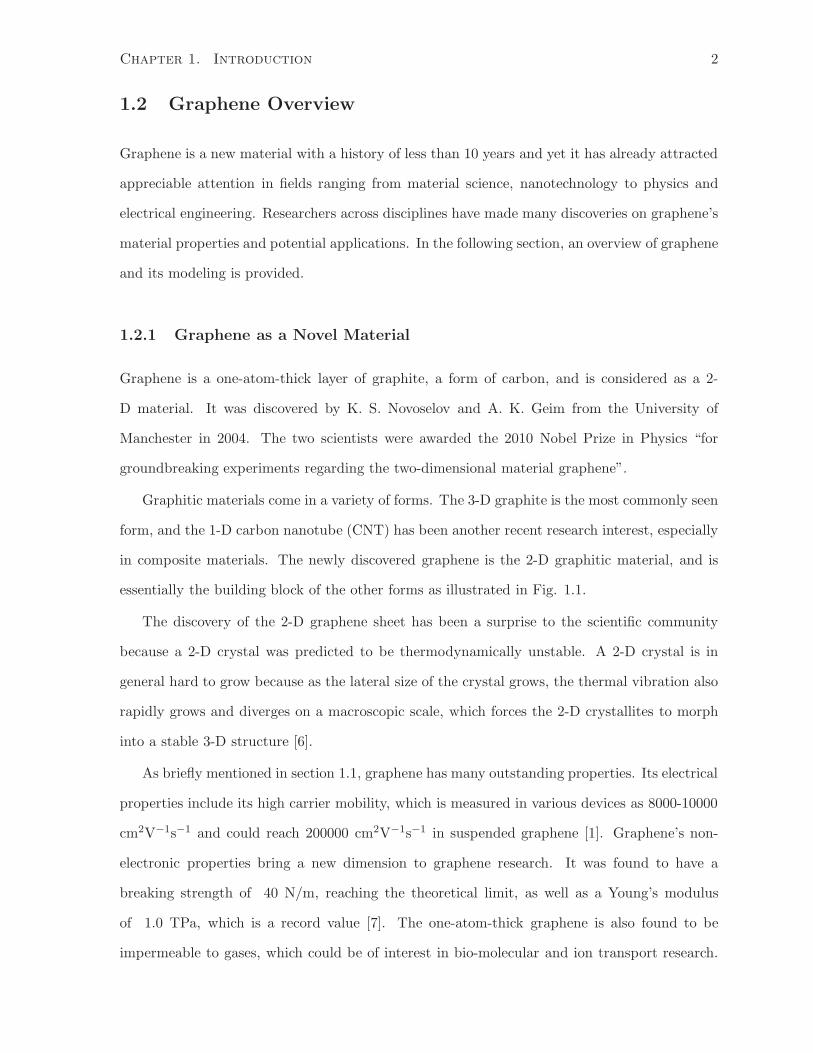
essentially the building block of the other forms as illustrated in Fig. 1.1.
The discovery of the 2-D graphene sheet has been a surprise to the scientific community
because a 2-D crystal was predicted to be thermodynamically unstable. A 2-D crystal is in
general hard to grow because as the lateral size of the crystal grows, the thermal vibration also
rapidly grows and diverges on a macroscopic scale, which forces the 2-D crystallites to morph
into a stable 3-D structure [6].
As briefly mentioned in section 1.1, graphene has many outstanding properties. Its electrical
properties include its high carrier mobility, which is measured in various devices as 8000-10000
cm2V−1s−1 and could reach 200000 cm2V−1s−1 in suspended graphene [1]. Graphene’s non-
electronic properties bring a new dimension to graphene research. It was found to have a
breaking strength of 40 N/m, reaching the theoretical limit, as well as a Young’s modulus
of 1.0 TPa, which is a record value [7]. The one-atom-thick graphene is also found to be
impermeable to gases, which could be of interest in bio-molecular and ion transport research.

Chapter 1. Introduction 3
Figure 1.1: Graphitic materials in various dimensionalities: 0-D buckyball, 1-D carbon nan-otube, 2-D graphene and 3-D graphite [5].
Chapter 1. Introduction 4
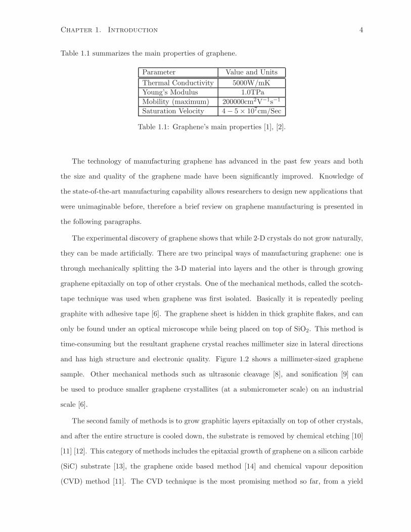
Table 1.1 summarizes the main properties of graphene.
Parameter Value and Units
Thermal Conductivity 5000W/mK
Young’s Modulus 1.0TPa
Mobility (maximum) 200000cm2V−1s−1
Saturation Velocity 4− 5× 107cm/Sec
Table 1.1: Graphene’s main properties [1], [2].
The technology of manufacturing graphene has advanced in the past few years and both
the size and quality of the graphene made have been significantly improved. Knowledge of
the state-of-the-art manufacturing capability allows researchers to design new applications that
were unimaginable before, therefore a brief review on graphene manufacturing is presented in
the following paragraphs.
The experimental discovery of graphene shows that while 2-D crystals do not grow naturally,
they can be made artificially. There are two principal ways of manufacturing graphene: one is
through mechanically splitting the 3-D material into layers and the other is through growing
graphene epitaxially on top of other crystals. One of the mechanical methods, called the scotch-
tape technique was used when graphene was first isolated. Basically it is repeatedly peeling
graphite with adhesive tape [6]. The graphene sheet is hidden in thick graphite flakes, and can
only be found under an optical microscope while being placed on top of SiO2. This method is
time-consuming but the resultant graphene crystal reaches millimeter size in lateral directions
and has high structure and electronic quality. Figure 1.2 shows a millimeter-sized graphene
sample. Other mechanical methods such as ultrasonic cleavage [8], and sonification [9] can
be used to produce smaller graphene crystallites (at a submicrometer scale) on an industrial
scale [6].
The second family of methods is to grow graphitic layers epitaxially on top of other crystals,
and after the entire structure is cooled down, the substrate is removed by chemical etching [10]
[11] [12]. This category of methods includes the epitaxial growth of graphene on a silicon carbide
(SiC) substrate [13], the graphene oxide based method [14] and chemical vapour deposition
(CVD) method [11]. The CVD technique is the most promising method so far, from a yield

Chapter 1. Introduction 5
and quality point of view. A 76.2cm (30 in) graphene film has been fabricated on a copper
substrate using the CVD technique and has been further processed to make a graphene based
touch screen [15]. The aforementioned graphene properties and current level of manufacturing
capability make graphene a good candidate for many novel devices as will be introduced in the
next section.
Figure 1.2: A graphene sample at the millimeter scale.
1.2.2 Graphene Applications
As silicon-based technology approaches its fundamental limits, the electronics industry is look-
ing for an alternative material to replace silicon in order to further shrink the device size.
Graphene’s ultra-thin nature and its electrical properties make it a good candidate and this
brings more attention and input to graphene research. Graphene field-effect transistors (FET)
and graphene wafer scale integrated circuits have been fabricated and versatile graphene appli-
cations in EM and transformation optics has been developed in recent years. Several designs
emerged from graphene’s unique properties will be presented in the following sections.
A Graphene Field-effect Transistor (FET)
Graphene’s high carrier mobility and saturation velocity make it a promising candidate for
high-speed electronics and radio-frequency applications. Since the transistor is the most basic
element of electronic circuits, building graphene-based transistors opens up the possibilities for
a wider range of graphene based applications.
Chapter 1. Introduction 6
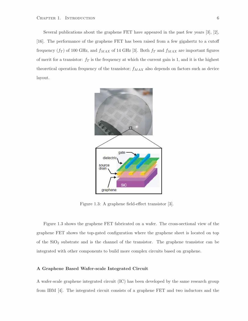
Several publications about the graphene FET have appeared in the past few years [3], [2],
[16]. The performance of the graphene FET has been raised from a few gigahertz to a cutoff
frequency (fT ) of 100 GHz, and fMAX of 14 GHz [3]. Both fT and fMAX are important figures
of merit for a transistor: fT is the frequency at which the current gain is 1, and it is the highest
theoretical operation frequency of the transistor; fMAX also depends on factors such as device
layout.
Figure 1.3: A graphene field-effect transistor [3].
Figure 1.3 shows the graphene FET fabricated on a wafer. The cross-sectional view of the
graphene FET shows the top-gated configuration where the graphene sheet is located on top
of the SiO2 substrate and is the channel of the transistor. The graphene transistor can be
integrated with other components to build more complex circuits based on graphene.
A Graphene Based Wafer-scale Integrated Circuit
A wafer-scale graphene integrated circuit (IC) has been developed by the same research group
from IBM [4]. The integrated circuit consists of a graphene FET and two inductors and the

Chapter 1. Introduction 7
integrated circuit operates as a broadband radio-frequency mixer at frequencies up to 10 GHz.
The gate length for the graphene transistor is 550nm; the inductors are made of 1µm thick
aluminium. The schematic and optical images of the circuit are shown in Fig. 1.4.
(a) (b)
Figure 1.4: (a) Schematics of the graphene mixer circuit (b) Optical images of graphene ICs. [4]
The challenges in making a graphene based IC come from the distinct material properties
of graphene comparing to the conventional semiconductors, for example, its poor adhesion with
metals and oxides, and its vulnerability to damage in plasma processing. The final circuit is
fabricated on a SiC substrate, and is less than 1mm2 including the contact pads. The graphene
mixer has a 27 dB conversion loss at 4 GHz, compared to a 7 dB conversion loss at 1.95 GHz
for GaAs-based mixer. The authors suggest that by using high-k dielectrics or highly scaled
gate lengths, for example a 40nm gate, it is possible to improve the conversion gain by more
than 20 dB.
Graphene Coplanar Waveguide (CPW)
Unlike in carbon nanotubes, a 50Ω characteristic impedance can be obtained in graphene, and
this fact opens up the perspective to the graphene based RF applications. As an example, a
graphene based coplanar waveguide (CPW) has been developed in [17]. The CPW operates up
to 65 GHz. One of the challenges encountered in making of the CPW comes from the limited

Chapter 1. Introduction 8
size of the graphene flake for this experiment. The CPW has a dimension of 25µm × 80µm
and the graphene flake is large enough to pattern the CPW but not the probe tip which has a
size of 150µm. Therefore the electrodes are extended and enlarged on the SiO2 substrate to fit
the probe tips.
(a) (b) (c)
Figure 1.5: (a) The graphene sample used to fabricate the CPW [18] (b) The position of theCPW electrodes over graphene [18] (c) Optical images of graphene CPW [17].
Fig. 1.5(a) shows the graphene sample used to fabricate the graphene CPW, Fig. 1.5(b)
shows the positioning of the CPW electrodes over the graphene flake and Fig. 1.5(c) presents
the optical image of the graphene CPW, illustrating the extended electrodes; the graphene layer
is not visible on this photo.
Graphene Nano-antenna
Earlier research on nano-antenna was focusing on the carbon nanotube (CNT) based antennas.
CNTs support slow-wave propagation, whereby the phase velocity of electromagnetic waves
propagating in CNT is on the order of c0/100 to c0/50 (c0 being the speed of light in a vaccum)
[19], therefore CNT nano-antennas are usually much shorter than the free-space wavelength and
are electrically small. This feature enables the miniaturization of the structures. One drawback
of the CNT antenna is its high resistance. Due to its extremely high aspect ratio (length/cross
sectional area) of the CNT, the resistance reaches several kilo-ohm per micrometer. As a result
of the high resistance, the CNT nano-antenna often has a low efficiency. Fig. 1.6 shows a CNT
antenna and a graphene nanoribbon (GNR) antenna.
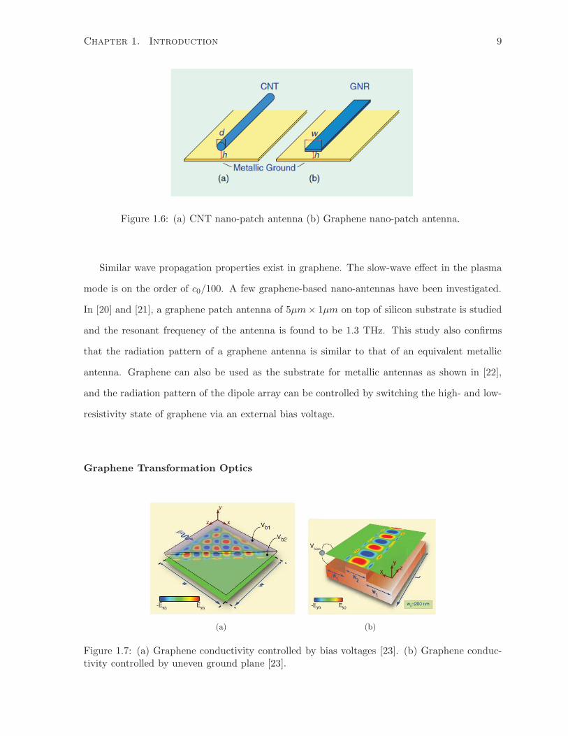
Chapter 1. Introduction 9
Figure 1.6: (a) CNT nano-patch antenna (b) Graphene nano-patch antenna.
Similar wave propagation properties exist in graphene. The slow-wave effect in the plasma
mode is on the order of c0/100. A few graphene-based nano-antennas have been investigated.
In [20] and [21], a graphene patch antenna of 5µm× 1µm on top of silicon substrate is studied
and the resonant frequency of the antenna is found to be 1.3 THz. This study also confirms
that the radiation pattern of a graphene antenna is similar to that of an equivalent metallic
antenna. Graphene can also be used as the substrate for metallic antennas as shown in [22],
and the radiation pattern of the dipole array can be controlled by switching the high- and low-
resistivity state of graphene via an external bias voltage.
Graphene Transformation Optics
(a) (b)
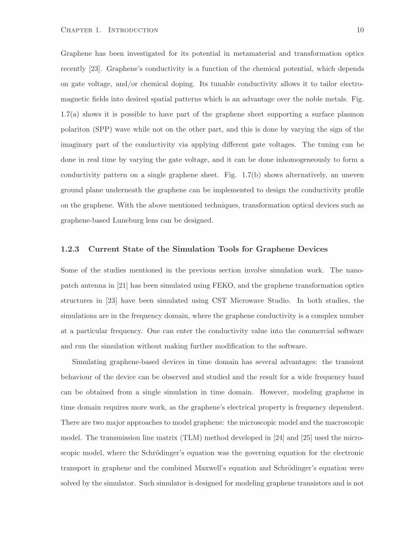
Figure 1.7: (a) Graphene conductivity controlled by bias voltages [23]. (b) Graphene conduc-tivity controlled by uneven ground plane [23].
Chapter 1. Introduction 10
Graphene has been investigated for its potential in metamaterial and transformation optics
recently [23]. Graphene’s conductivity is a function of the chemical potential, which depends
on gate voltage, and/or chemical doping. Its tunable conductivity allows it to tailor electro-
magnetic fields into desired spatial patterns which is an advantage over the noble metals. Fig.
1.7(a) shows it is possible to have part of the graphene sheet supporting a surface plasmon
polariton (SPP) wave while not on the other part, and this is done by varying the sign of the
imaginary part of the conductivity via applying different gate voltages. The tuning can be
done in real time by varying the gate voltage, and it can be done inhomogeneously to form a
conductivity pattern on a single graphene sheet. Fig. 1.7(b) shows alternatively, an uneven
ground plane underneath the graphene can be implemented to design the conductivity profile
on the graphene. With the above mentioned techniques, transformation optical devices such as
graphene-based Luneburg lens can be designed.
1.2.3 Current State of the Simulation Tools for Graphene Devices
Some of the studies mentioned in the previous section involve simulation work. The nano-
patch antenna in [21] has been simulated using FEKO, and the graphene transformation optics
structures in [23] have been simulated using CST Microwave Studio. In both studies, the
simulations are in the frequency domain, where the graphene conductivity is a complex number
at a particular frequency. One can enter the conductivity value into the commercial software
and run the simulation without making further modification to the software.
Simulating graphene-based devices in time domain has several advantages: the transient
behaviour of the device can be observed and studied and the result for a wide frequency band
can be obtained from a single simulation in time domain. However, modeling graphene in
time domain requires more work, as the graphene’s electrical property is frequency dependent.
There are two major approaches to model graphene: the microscopic model and the macroscopic
model. The transmission line matrix (TLM) method developed in [24] and [25] used the micro-
scopic model, where the Schrodinger’s equation was the governing equation for the electronic
transport in graphene and the combined Maxwell’s equation and Schrodinger’s equation were
solved by the simulator. Such simulator is designed for modeling graphene transistors and is not
Chapter 1. Introduction 11
applicable to study macroscopic devices such as graphene-based waveguides at current stage.
The macroscopic model uses a conductivity model to represent graphene property. It has been
used in some of the analytical studies on graphene [26], [27], as well as in graphene simulation
based on FDTD method [28], because it is easier to incorporate the macroscopic model into the
general FDTD scheme. In [28], a sub-cell model was used to model the graphene sheet, and a
periodic boundary condition (PBC) was applied to terminate the simulation domain. With the
PBC in place, only simulations with normal incidence waves can be supported and the use of
point sources or oblique incidence waves was not possible with the existing scheme. The limi-
tation of the simulation scheme resulted from the use of PBC can be removed by introducing
a perfectly matched layer (PML) to terminate the simulation domain.
In this thesis, a novel sub-cell PML technique is developed to simulate graphene-based
devices using the FDTD method. The use of sub-cell model reduces computational cost of
the FDTD simulations compared to using regular FDTD mesh, and using PML for boundary
condition allows a wider selection of applications to be studied compared to the FDTD scheme
based on PBC [28]. In addition, it is a general technique and can be applied to study a variety
of dispersive or dielectric thin layer structures.
1.3 Outline
This thesis starts with the study of the FDTD modeling of graphene. In Chapter 2, the
graphene conductivity model is introduced, and the FDTD update equations for graphene are
developed. The dispersion and stability study for intra-band conductivity is presented, and
such analysis serves as a basis for the simulation work presented in later chapters. Chapters
3 and 4 present the novel sub-cell PML framework developed for simulating graphene-based
devices: the background of the techniques involved is included, the detailed implementation
of the method is presented and the test results of the framework with various 2-D and 3-D
dielectric and graphene structures are shown and discussed. In Chapter 5, a graphene-based
patch antenna is studied in 2-D. Chapter 6 concludes this thesis, with a summary of work done
and contributions along with possible future work related to this thesis.

Chapter 2
FDTD Modeling of Graphene
As mentioned in section 1.2.3, the macroscopic graphene conductivity model is used when sim-
ulating graphene based devices using the FDTD method. In this chapter, the macroscopic
graphene conductivity model is introduced, the FDTD update equations for graphene are de-
rived and the dispersion and stability analysis for the update scheme are provided.
2.1 Graphene Conductivity Model
The graphene surface conductivity (in unit of [S]) is given by the Kubo formula [29]:
σ(ω, µc, γ, T ) =je2(ω − j2γ)
πh2
[
1
(ω − j2γ)2
∫
∞
0ǫ
(
∂fd(ǫ)
∂ǫ− ∂fd(−ǫ)
∂ǫ
)
dǫ
−∫
∞
0
fd(−ǫ)− fd(ǫ)
(ω − j2γ)2 − 4(ǫ/h)2dǫ
]
. (2.1)
In equation (2.1), fd(ǫ) = (e(ǫ−µc)/kBT + 1)−1 is the Fermi-Dirac distribution, ω is the angular
frequency in radians and γ is the scattering rate in s−1. Also, µc is the chemical potential
in eV, which can be controlled by chemical doping or by applying a bias voltage, T is the
temperature in Kelvin, −e is the electron charge, h is the reduced Planck’s constant, and kB is
the Boltzmann constant. The first term in equation (2.1) is due to the intra-band contribution,
and the second term is from the inter-band contribution.
12

Chapter 2. FDTD Modeling of Graphene 13
The Kubo formula is in an integral form which makes it hard to evaluate as well as to
integrate with the FDTD scheme. The Kubo formula can be simplified [26], and the intra-band
conductivity is:
σintra(ω, µc, γ, T ) =je2kBT
πh2
(
µc
kBT+ 2 ln(e(−µc/kBT ) + 1)
)
1
ω − j2γ, (2.2)
and the inter-band conductivity is as follows:
σinter(ω, µc, γ, 0) =−je2
4πhln
(
2|µc|−(ω − j2γ)h
2|µc|+(ω − j2γ)h
)
. (2.3)
The intra-band conductivity mainly accounts for the low frequency electrical transport and
the inter-band conductivity is for the optical excitations. The work presented in this thesis is
mainly in the microwave frequency range. Taking the parameters used in the graphene parallel
plate waveguide study [27] as an example, µc = 0.5eV, γ = 1012 and T = 0K, the corresponding
conductivity values are plotted in Fig. 2.1. Fig. 2.2 shows the conductivity value for a range
of chemical potential.
0 200 400 600 800 1000 1200−0.02
0
0.02
0.04
σ intr
a (S
)
Re(σintra
) Im (σintra
)
0 200 400 600 800 1000 12000
0.5
1
1.5
2x 10
−7
frequency (GHz)
σ inte
r (S
)
Re(σinter
) Im(σinter
)
Figure 2.1: Graphene surface conductivity for µc = 0.5eV, γ = 1012 and T = 0.
From Fig. 2.1 and 2.2, we can see that in the frequency range up to 800 GHz, the value of

Chapter 2. FDTD Modeling of Graphene 14
0 200 400 600 8000
0.1
0.2
0.3
0.4
0.5
σintra
real part (S)
frequency (GHz)
chem
ical
pot
entia
l µc (
eV)
−0.01
0
0.01
0.02
0.03
0.04
0 200 400 600 8000
0.1
0.2
0.3
0.4
0.5
σintra
imaginary part (S)
frequency (GHz)
chem
ical
pot
entia
l µc (
eV)
−0.01
0
0.01
0.02
0.03
0.04
0 200 400 600 8000
0.1
0.2
0.3
0.4
0.5
σinter
real part (S)
frequency (GHz)
chem
ical
pot
entia
l µc (
eV)
0.5
1
1.5
2
2.5x 10
−6
0 200 400 600 8000
0.1
0.2
0.3
0.4
0.5
σinter
imaginary part (S)
frequency (GHz)
chem
ical
pot
entia
l µc (
eV)
1
2
3
4
5
6
x 10−6
Figure 2.2: Graphene surface conductivity for µc = 0− 0.5eV, γ = 1012 and T = 0.

Chapter 2. FDTD Modeling of Graphene 15
σintra dominates over that of σinter. Therefore, σinter can be ignored for most simulations below
optical frequencies.
If we take a closer look at the formula for σintra, the expression is actually a Drude model:
σintra,s =Q′
jω + 2γ, (2.4)
where
Q′ =e2kBT
πh2
(
µc
kBT+ 2 ln(e(−µc/kBT ) + 1)
)
. (2.5)
The surface conductivity (in unit of [S]) can be converted to the volumetric conductivity (in
unit of [S/m]) by dividing equation (2.4) by the thickness of graphene, which is assumed to
be 10−9m or 1 nm here. Using a different thickness value around 1 nm would not result in
a significant change in simulation result as stated in [23]. If the thickness value used in a
simulation is deviated from 1 nm by a large margin, the accuracy of the simulation result could
be affected because the geometry of the structure is not modeled properly. The stability of the
updating scheme is not affected by the thickness value used. The volumetric conductivity is
then given by:
σintra,v =σintra,s10−9
, (2.6)
σintra,v =Q
jω + 2γ, (2.7)
where
Q(µc, T ) =Q′
10−9=
e2kBT
πh2
(
µc
kBT+ 2 ln(e(−µc)/(kBT ) + 1)
)
/10−9. (2.8)
To find the relative permittivity (ǫr) from the conductivity, the following equations are used:
ǫr = ǫ′ − jǫ′′, (2.9)
ǫ′′ =σ
ωǫ0, (2.10)
ǫr = 1− jσ
ωǫ0, (2.11)
ǫr = 1 +Q
jωǫ0(jω + 2γ)= 1 +
Q/ǫ0−ω2 + 2γjω
. (2.12)
Chapter 2. FDTD Modeling of Graphene 16
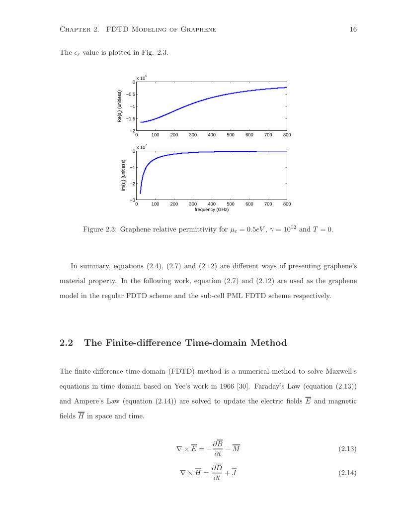
The ǫr value is plotted in Fig. 2.3.
0 100 200 300 400 500 600 700 800−2
−1.5
−1
−0.5
0x 10
6
Re
ε r (u
nitle
ss)
0 100 200 300 400 500 600 700 800−3
−2
−1
0x 10
7
frequency (GHz)
Imε
r (u
nitle
ss)
Figure 2.3: Graphene relative permittivity for µc = 0.5eV , γ = 1012 and T = 0.
In summary, equations (2.4), (2.7) and (2.12) are different ways of presenting graphene’s
material property. In the following work, equation (2.7) and (2.12) are used as the graphene
model in the regular FDTD scheme and the sub-cell PML FDTD scheme respectively.
2.2 The Finite-difference Time-domain Method
The finite-difference time-domain (FDTD) method is a numerical method to solve Maxwell’s
equations in time domain based on Yee’s work in 1966 [30]. Faraday’s Law (equation (2.13))
and Ampere’s Law (equation (2.14)) are solved to update the electric fields E and magnetic
fields H in space and time.
∇× E = −∂B
∂t−M (2.13)
∇×H =∂D
∂t+ J (2.14)

Chapter 2. FDTD Modeling of Graphene 17
The constitutive relations for the electric flux density D and the magnetic flux density B are
as follows:
D = ǫE = ǫ0ǫrE, (2.15)
B = µH = µ0µrH. (2.16)
Assuming J = 0 and M = 0, the two Maxwell’s curl equations (2.13), (2.14) in Cartesian
coordinates can be written as:
∂Ex
∂t=
1
ǫ
[
∂Hz
∂y− ∂Hy
∂z
]
(2.17a)
∂Ey
∂t=
1
ǫ
[
∂Hx
∂z− ∂Hz
∂x
]
(2.17b)
∂Ez
∂t=
1
ǫ
[
∂Hy
∂x− ∂Hx
∂y
]
(2.17c)
∂Hx
∂t=
1
µ
[
∂Ey
∂z− ∂Ez
∂y
]
(2.18a)
∂Hy
∂t=
1
µ
[
∂Ez
∂x− ∂Ex
∂z
]
(2.18b)
∂Hz
∂t=
1
µ
[
∂Ex
∂y− ∂Ey
∂x
]
. (2.18c)
In [30], the Yee’s cell of dimension ∆x×∆y×∆z is introduced as a unit cell of the discretized
spatial domain as shown in Fig. 2.4. The E fields and H fields are defined in an interlinked
way such that each E node is surrounded by 4 H nodes and vice versa, and the E nodes and
H nodes are dislocated by half a cell spatially.
All fields are initially set to zero in the simulation domain. With a source excitation, all E
fields are updated at the integer time step n, and H fields are updated at half time steps n+ 12
using the E values at time step n. Repeating this process allows the simulation to march in
time.
A second order accurate, centered finite-difference approximation is applied to discretize the

Chapter 2. FDTD Modeling of Graphene 18
x
y
z
Δx
Δy
Δz
Hx
Hy
Hx
Hx
Hy
Hy
Hz Hz
Hz
Ez
Ey
Ex
Figure 2.4: Yee’s cell with E and H fields positions in the unit cell.
partial derivatives in equations (2.17) and (2.18) as follows:
∂Fn(i, j, k)
∂x=
Fn(i+ 0.5, j, k) − Fn(i− 0.5, j, k)
∆x+O(∆x2), (2.19a)
∂Fn(i, j, k)
∂t=
Fn+0.5(i, j, k) − Fn−0.5(i, j, k)
∆t+O(∆t2), (2.19b)
where i, j, k are space indices in x−, y−, z− directions respectively and n is the temporal index;
Fn(i, j, k) = F (i∆x, j∆y, k∆z, n∆t). Following the discretization method in equation (2.19),
the FDTD update equations for (2.17a) and (2.18a) can be obtained as:
En+1x,(i,j,k) =En
x,(i,j,k) +∆t
ǫ
(
1
∆y
(
Hn+0.5z,(i+0.5,j+0.5,k) −Hn+0.5
z,(i+0.5,j−0.5,k)
)
− 1
∆z
(
Hn+0.5y,(i+0.5,j,k+0.5) −Hn+0.5
y,(i+0.5,j,k−0.5)
)
)
,
(2.20)
Hn+0.5x,(i,j+0.5,k+0.5)
=Hn−0.5x,(i,j+0.5,k+0.5)
− ∆t
µ
(
1
∆y(En
z,(i,j+1,k+0.5) − Enz,(i,j,k+0.5))
− 1
∆x(En
y,(i,j+0.5,k+1) − Eny,(i,j+0.5,k))
)
.
(2.21)
The update equations for other E and H components can be derived in a similar way.

Chapter 2. FDTD Modeling of Graphene 19
2.3 FDTD Update Equations for Graphene at Microwave Fre-
quencies
The FDTD update equations for graphene at microwave frequencies involve σintra only. The
conduction current (J) can be updated as:
J = σintra,vE =Q
jω + 2γE, (2.22a)
∂
∂tJ + 2γJ = QE, (2.22b)
Jn+1 − J
n
∆t+ 2γ
Jn+1
+ Jn
2= Q
En+1
+ En
2, (2.22c)
Jn+1
=1− γ∆T
1 + γ∆TJn+
Q∆t
2(1 + γ∆t)(E
n+1+ E
n). (2.22d)
The Jn+0.5
term will be needed when updating En:
Jn+0.5
=1
2(J
n+1+ J
n) =
1
1 + γ∆tJn+
Q∆t
4(1 + γ∆t)(E
n+1+ E
n). (2.23)
The E fields can be updated as:
En+1
= En − ∆t
ǫ∇×H
n+0.5 − ∆t
2ǫ(J
n+1+ J
n), (2.24a)
En+1
=
ǫ∆t −
Q∆t4(1+γ∆t)
ǫ∆t +
Q∆t4(1+γ∆t)
En − 1
(1 + γ∆t)(
ǫ∆t +
Q∆t4(1+γ∆t)
)Jn+∇×H. (2.24b)
The update equation for H fields follow as:
Hn+0.5
= Hn−0.5 − ∆t
µ∇× E
n+0.5. (2.25)
The discretized 3-D update equations for graphene are listed below:
Jn+1x,(i+0.5,j,k) =
1− γ∆T
1 + γ∆TJnx,(i+0.5,j,k) +
Q∆t
2(1 + γ∆t)(En+1
x,(i+0.5,j,k) + Enx,(i+0.5,j,k)) (2.26)
Jn+1y,(i,j+0.5,k) =
1− γ∆T
1 + γ∆TJny,(i,j+0.5,k) +
Q∆t
2(1 + γ∆t)(En+1
y,(i,j+0.5,k) + Eny,(i,j+0.5,k)) (2.27)
Chapter 2. FDTD Modeling of Graphene 20
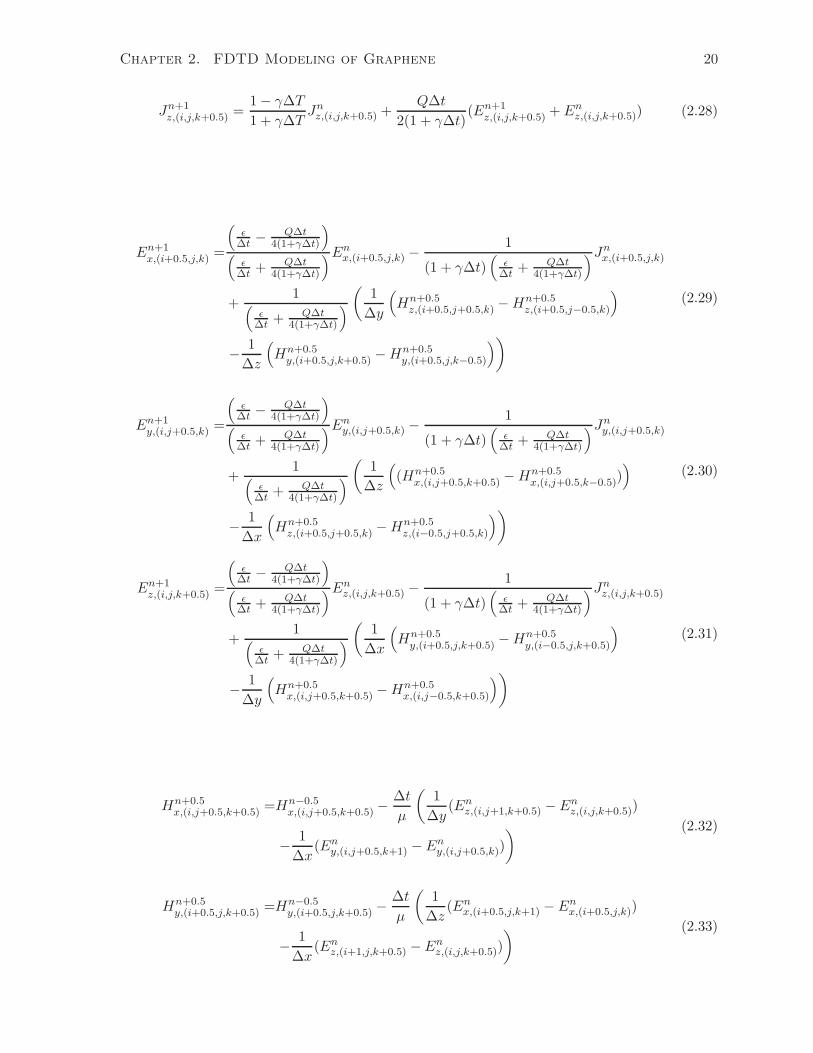
Jn+1z,(i,j,k+0.5) =
1− γ∆T
1 + γ∆TJnz,(i,j,k+0.5) +
Q∆t
2(1 + γ∆t)(En+1
z,(i,j,k+0.5) + Enz,(i,j,k+0.5)) (2.28)
En+1x,(i+0.5,j,k) =
(
ǫ∆t −
Q∆t4(1+γ∆t)
)
(
ǫ∆t +
Q∆t4(1+γ∆t)
)Enx,(i+0.5,j,k) −
1
(1 + γ∆t)(
ǫ∆t +
Q∆t4(1+γ∆t)
)Jnx,(i+0.5,j,k)
+1
(
ǫ∆t +
Q∆t4(1+γ∆t)
)
(
1
∆y
(
Hn+0.5z,(i+0.5,j+0.5,k) −Hn+0.5
z,(i+0.5,j−0.5,k)
)
− 1
∆z
(
Hn+0.5y,(i+0.5,j,k+0.5) −Hn+0.5
y,(i+0.5,j,k−0.5)
)
)
(2.29)
En+1y,(i,j+0.5,k) =
(
ǫ∆t −
Q∆t4(1+γ∆t)
)
(
ǫ∆t +
Q∆t4(1+γ∆t)
)Eny,(i,j+0.5,k) −
1
(1 + γ∆t)(
ǫ∆t +
Q∆t4(1+γ∆t)
)Jny,(i,j+0.5,k)
+1
(
ǫ∆t +
Q∆t4(1+γ∆t)
)
(
1
∆z
(
(Hn+0.5x,(i,j+0.5,k+0.5) −Hn+0.5
x,(i,j+0.5,k−0.5)))
− 1
∆x
(
Hn+0.5z,(i+0.5,j+0.5,k) −Hn+0.5
z,(i−0.5,j+0.5,k)
)
)
(2.30)
En+1z,(i,j,k+0.5) =
(
ǫ∆t −
Q∆t4(1+γ∆t)
)
(
ǫ∆t +
Q∆t4(1+γ∆t)
)Enz,(i,j,k+0.5) −
1
(1 + γ∆t)(
ǫ∆t +
Q∆t4(1+γ∆t)
)Jnz,(i,j,k+0.5)
+1
(
ǫ∆t +
Q∆t4(1+γ∆t)
)
(
1
∆x
(
Hn+0.5y,(i+0.5,j,k+0.5) −Hn+0.5
y,(i−0.5,j,k+0.5)
)
− 1
∆y
(
Hn+0.5x,(i,j+0.5,k+0.5) −Hn+0.5
x,(i,j−0.5,k+0.5)
)
)
(2.31)
Hn+0.5x,(i,j+0.5,k+0.5) =Hn−0.5
x,(i,j+0.5,k+0.5) −∆t
µ
(
1
∆y(En
z,(i,j+1,k+0.5) − Enz,(i,j,k+0.5))
− 1
∆x(En
y,(i,j+0.5,k+1) − Eny,(i,j+0.5,k))
) (2.32)
Hn+0.5y,(i+0.5,j,k+0.5) =Hn−0.5
y,(i+0.5,j,k+0.5) −∆t
µ
(
1
∆z(En
x,(i+0.5,j,k+1) − Enx,(i+0.5,j,k))
− 1
∆x(En
z,(i+1,j,k+0.5) − Enz,(i,j,k+0.5))
) (2.33)
Chapter 2. FDTD Modeling of Graphene 21
Hn+0.5z,(i+0.5,j+0.5,k) =Hn−0.5
z,(i+0.5,j+0.5,k) −∆t
µ
(
1
∆x(En
y,(i+1,j+0.5,k) − Eny,(i,j+0.5,k))
− 1
∆y(En
x,(i+0.5,j+1,k) − Enx,(i+0.5,j,k))
) (2.34)
2.4 Dispersion and Stability Study: Intra-band Conductivity
To derive the dispersion relation, the von Neumann method is used here. Substituting a discrete
travelling wave solution u = ej(ω∆t−kd∆d) (d is direction: x, y or z) into equations (2.26)-(2.34),
the dispersion relation is:
(
λe−j0.5ω∆t − ej0.5ω∆t)
(
4 sin2(
ω∆t
2
)
−4∆t2
ǫµ∆x2sin2
(
kx∆x
2
)
− 4∆t2
ǫµ∆y2sin2
(
ky∆y
2
)
− 4∆t2
ǫµ∆z2sin2
(
kz∆z
2
))
+ (4j)P cos2(
ω∆t
2
)
sin
(
ω∆t
2
)
= 0,
(2.35)
where λ = 1−γ∆T1+γ∆T and P = P∆t
ǫ = Q∆t2
2ǫ(1+γ∆t) . The dispersion relation can be further simplified
by substituting g = ejω∆t into (2.35). g is the growth factor and needs to be less than or equal
to 1 for the updating scheme to be stable [31]. After doing some algebra, the dispersion relation
is as follows:
Wg3 +Xg2 + Y g + Z = 0, (2.36)
where
W =P
2+ 1, (2.37a)
X =P
2− λ+ (D − 2), (2.37b)
Y = 1− (D − 2)λ− P
2, (2.37c)
Z = −λ− P
2, (2.37d)
and
D = 4
(
∆t2c2
∆x2sin2
(
kx∆x
2
)
+∆t2c2
∆y2sin2
(
ky∆y
2
)
+∆t2c2
∆z2sin2
(
kz∆z
2
))
. (2.38)

Chapter 2. FDTD Modeling of Graphene 22
To derive a closed form stability criterion, the Routh-Hurwitz criterion is evaluated [31]. Apply
the following transformation mapping to the dispersion equation:
g =r + 1
r − 1. (2.39)
This transforms the exterior of the unit circle for g in the Z−plane to the right half of the
r−plane, and the stability condition is met if there is no roots in the right half plane of the
r−plane. Applying the transformation in (2.39) to (2.36):
a3r3 + a2r
2 + a1r + a0 = 0, (2.40)
where
a3 = W +X + Y + Z = D(1− λ), (2.41a)
a2 = 3W +X − Y − 3Z = 4P +D(λ+ 1), (2.41b)
a1 = 3W −X − Y + 3Z = (D − 4)(λ − 1), (2.41c)
a0 = (4−D)(λ+ 1). (2.41d)
A Routh table [31] for (2.40) is constructed:
a3 a1a2 a0
a1 − a3a0a2
0
a0 0
Table 2.1: Routh table for equation (2.40).
To achieve stability, the first column of the Routh table needs to be non-negative. Given
γ > 0 and Q > 0, this translates to:
(
∆t2c2
∆x2sin2
(
kx∆x
2
)
+∆t2c2
∆y2sin2
(
ky∆y
2
)
+∆t2c2
∆z2sin2
(
kz∆z
2
))
< 1. (2.42)
To simplify the expression, assume the worst case where sin2(
kx∆x2
)
= sin2(
ky∆y2
)
= sin2(
kz∆z2
)
=

Chapter 2. FDTD Modeling of Graphene 23
1. Then, equation (2.42) becomes
S =∆t2c2
∆x2+
∆t2c2
∆y2+
∆t2c2
∆z2< 1, (2.43)
which is the CFL limit of the regular 3-D FDTD update equations.
The above analysis shows that the stability condition for the graphene update equations is
the same as the CFL limit for the conventional FDTD method. The stability condition for the
1-D and 2-D case can be derived following the same method.
A more detailed derivation of the dispersion relation and stability condition is provided in
Appendix A.
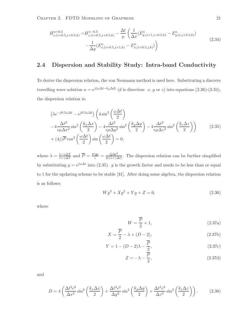
2.5 Study of the Numerical Wave Number in 1-D
The analysis of the accuracy of the numerical scheme is carried out by comparing the numerical
wavenumber k with the analytical k in 1-D case. The graphene parameters used are µc = 0.5eV ,
γ = 1012 and T = 0K. The analytical wave number for wave propagating in graphene is
calculated as
kz = ω√ǫ0µ0ǫr, (2.44)
where ǫr = 1− j σωǫ0
. The numerical wave number kz can be found from the dispersion relation
(2.35):
kz =1
∆zcos−1
(
1− 2
S2
(
jP cos2(πS/Nλ) sin(πS/Nλ)
Ce−jπS/Nλ − e−jπS/Nλ+ sin2
(
πS
Nλ
)))
. (2.45)
The real part of kz is the propagation constant βz, and the imaginary part is the attenuation
constant αz. Fig. 2.5 shows the comparison of the wave number extracted from a 1-D graphene
simulation with the analytical wave number as a function of frequency using ∆z = 5nm. The
result shows good agreement between the simulation and the analytical solution.
Chapter 2. FDTD Modeling of Graphene 24
100 200 300 400 500 600 700 8001
2
3
4
β (r
ad/µ
m)
β (theory)β (FDTD)
100 200 300 400 500 600 700 8000
5
10
frequency (GHz)
α (1
/µ m
)
α (theory)α (FDTD)
Figure 2.5: Comparison of theoretical and simulated β and α vs. frequency.
2.6 Modeling of Inter-band Conductivity
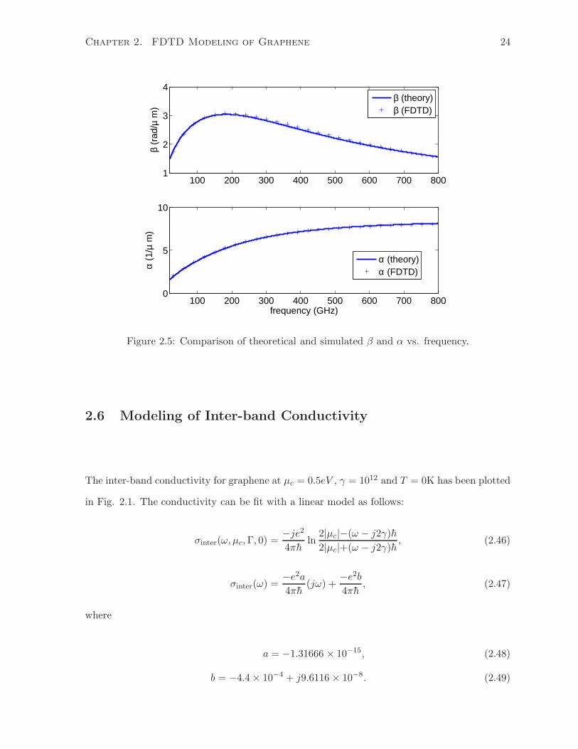
The inter-band conductivity for graphene at µc = 0.5eV , γ = 1012 and T = 0K has been plotted
in Fig. 2.1. The conductivity can be fit with a linear model as follows:
σinter(ω, µc,Γ, 0) =−je2
4πhln
2|µc|−(ω − j2γ)h
2|µc|+(ω − j2γ)h, (2.46)
σinter(ω) =−e2a
4πh(jω) +
−e2b
4πh, (2.47)
where
a = −1.31666 × 10⁻¹⁵, (2.48)
b = −4.4× 10⁻⁴ + j9.6116 × 10−8. (2.49)

Chapter 2. FDTD Modeling of Graphene 25
Equation (2.47) can be written as:
σinter(ω) = C(jω) +D (2.50)
C =−e2a
4πh, D =
−e2b
4πh. (2.51)
This model works for the frequency range where the conductivity can be fit as a straight
line. For a wider frequency range, one way to model it is to use a piecewise linear model, which
models a curve with several linear segments. One can find the different coefficients for each of
the segment and therefore form a model for a wide frequency range.
Aside from the piecewise linear model, a Pade approximation can also be applied to fit
the inter-band conductivity for graphene as introduced in [32]. A Pade approximation fits a
rational polynomial of the form:
a0 + a1ω + ...+ aMωM
1 + b1ω + ...+ bNωN= σinter(ω) (2.52)
to a set of data points. Since polynomials of order M = N = 2 are easy to fit in to the FDTD
scheme, it is chosen to model the graphene inter-band conductivity:
a0 + a1jω + a2(jω)2
1 + b1jω + b2(jω)2= σinter(ω). (2.53)
The optimal coefficients are found to be:
a0 = −9.114 × 10⁻²⁸ (2.54a)
a1 = 1.674 × 10⁻²⁰ (2.54b)
a2 = 1.343 × 10−36 (2.54c)
b1 = 8.082 × 10⁻¹⁷ (2.54d)
b2 = 2.148 × 10⁻³¹ (2.54e)
for a frequency range up to 2.2 × 10¹⁴ Hz [32].
Chapter 2. FDTD Modeling of Graphene 26
Either the linear model or the Pade approximation can be applied to model the graphene
inter-band conductivity, depending on the frequency range of interest and the complexity level
of a particular problem.
2.7 Summary
This chapter started with presenting the graphene conductivity model in various forms, with
a focus on the intra-band conductivity. A brief introduction to FDTD has been given and the
FDTD update equations for graphene in the microwave frequency range were derived. The von
Neumann method was used to derive the dispersion relation in the FDTD update equations for
graphene, and the Routh-Hurwitz criterion was evaluated to find the stability criterion. It has
been found that the stability condition for the graphene update equations was the CFL limit,
regardless of the value of chemical potential (µc) or temperature (T ), which affect the graphene
conductivity value. The numerical wave number extracted from a 1-D FDTD simulation was
compared with the analytical wave number for waves traveling in graphene. The matching
result confirmed that the FDTD model was accurate. The modeling of inter-band conductivity
has also been briefly discussed in this chapter. There are two approaches to model the inter-
band conductivity: the linear model and the Pade approximation. The linear model is easier
to implement and the Pade approximation covers a wider range of frequencies. The decision
on which model to use would depend on the nature of individual problems.

Chapter 3
Theory of Sub-cell Dispersive
Perfectly Matched Layer (PML)
The modeling of graphene using the regular FDTD mesh is computationally intensive, in terms
of both the memory requirement and the simulation time. Because of the ultra-thin nature
of graphene, the geometry of the test structure instead of the maximum frequency of interest
becomes the limiting factor of the spatial grid. An ultra-fine mesh in space and time would
result in a large simulation domain and long simulation time.
The sub-cell method [33] can be applied to reduce the computational cost by introducing a
sub-layer inside a Yee’s cell, and the spatial grid is not limited by the smallest physical feature
any more. This chapter presents a framework to simulate graphene based structures using the
sub-cell method and the dispersive PML.
3.1 Introduction to the Sub-cell Technique
The sub-cell model was first introduced in [33] to model thin material sheets that were perpen-
dicular to one of the major axes of the FDTD lattice. Fig. 3.1(a) shows a 3-D Yee’s cell with
a sub-layer in the yz plane. A sub-layer could be a material that has a different permittivity
and/or a different permeability from the rest of the cell. The sub-layer is inserted in x− direc-
tion with a thickness of α ×∆x, where ∆x is the x− dimension of the Yee’s cell and α is the
27

Chapter 3. Theory of Sub-cell Dispersive Perfectly Matched Layer (PML) 28
fraction of the cell occupied by the sub-layer. The sub-cell α needs to be less than 0.5. A 2-D
sub-cell model is shown in Fig. 3.1(b). The inserted layer becomes a slot in the 2-D model.
x
z
-y
Yee's cellSub-cell
layer
α·dxdx
(a)
x
z
Yee's cell
Sub-cell
layer
α·dx
dx
(b)
Figure 3.1: (a) A 3-D sub-cell model (b) A 2-D sub-cell model in the xz plane.
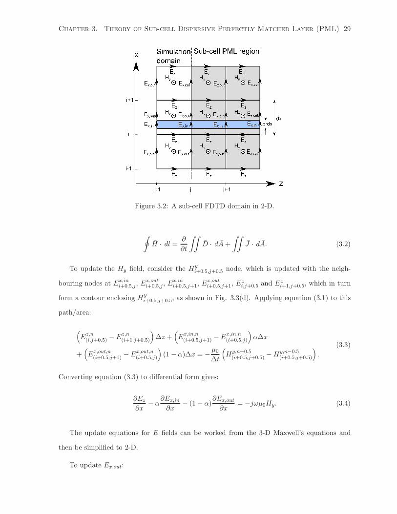
To find the update equations for the sub-cell scheme, new field nodes are introduced to
model the sub-layer. For the 2-D model in Fig. 3.1(b) with a sub-layer of different permittivity,
the electric field normal to the sheet, Ex, is split into two parts: Ex,in is the Ex field inside
the sub-layer and Ex,out is the Ex field for the rest of the cell. This allows the modeling of the
discontinuous permittivity on the material interface. The tangential electric field Ez and the
tangential magnetic field Hy are continuous across the material interface and therefore do not
need to be split. The field nodes to be updated are shown in Fig. 3.2.
Insertion of the sub-layer introduces uncertainty in the geometry of the structure because
one can not choose the exact location of the sub-layer within a Yee’s cell. The inserted layer
usually has an α value less than 0.5, and the lower limit of α depends on the geometry of the
structure and the accuracy level required for the simulation.
3.2 FDTD Update Equations for 2-D Sub-cell Scheme
The update equations for the 2-D sub-cell scheme involving a dispersive sub-layer can be derived
from the integral form of Maxwell’s equations as follows:
∮
E · dl = − ∂
∂t
∫∫
B · dA−∫∫
M · dA, (3.1)
Chapter 3. Theory of Sub-cell Dispersive Perfectly Matched Layer (PML) 29
Figure 3.2: A sub-cell FDTD domain in 2-D.
∮
H · dl = ∂
∂t
∫∫
D · dA+
∫∫
J · dA. (3.2)
To update the Hy field, consider the Hyi+0.5,j+0.5 node, which is updated with the neigh-
bouring nodes at Ex,ini+0.5,j, E
x,outi+0.5,j, E
x,ini+0.5,j+1, E
x,outi+0.5,j+1, E
zi,j+0.5 and Ez
i+1,j+0.5, which in turn
form a contour enclosing Hyi+0.5,j+0.5, as shown in Fig. 3.3(d). Applying equation (3.1) to this
path/area:
(
Ez,n(i,j+0.5) − Ez,n
(i+1,j+0.5)
)
∆z +(
Ex,in,n(i+0.5,j+1) −Ex,in,n
(i+0.5,j)
)
α∆x
+(
Ex,out,n(i+0.5,j+1) − Ex,out,n
(i+0.5,j)
)
(1− α)∆x = − µ0
∆t
(
Hy,n+0.5(i+0.5,j+0.5) −Hy,n−0.5
(i+0.5,j+0.5)
)
.
(3.3)
Converting equation (3.3) to differential form gives:
∂Ez
∂x− α
∂Ex,in
∂x− (1− α)
∂Ex,out
∂x= −jωµ0Hy. (3.4)
The update equations for E fields can be worked from the 3-D Maxwell’s equations and
then be simplified to 2-D.
To update Ex,out:

Chapter 3. Theory of Sub-cell Dispersive Perfectly Matched Layer (PML) 30
x
y
z
Hy Hy
Hz
Hz
Ex,out
x
y
z
Hy Hy
Hz
Hz
Ex,in
x
y
z
Ez Ez
Ex,out
Ex,out
Hy
Ex,in
Ex,in
z
x
y
Hx Hx
Hy
Hy
Ez
a) Updating Ex,out b) Updating Ex,in
c) Updating Ez d) Updating Hy
Figure 3.3: Integral contour of 3-D Maxwell’s equations.

Chapter 3. Theory of Sub-cell Dispersive Perfectly Matched Layer (PML) 31
(
Hy,n+0.5(i+0.5,j,k−0.5) −Hy,n+0.5
(i+0.5,j,k+0.5)
)
∆y +(
Hz,n+0.5(i+0.5,j+0.5,k) −Hz,n+0.5
(i−0.5,j−0.5,k)
)
∆z
=ǫ0∆t
Ex,out,n+0.5(i+0.5,j,k) ∆y∆z
(3.5)
To convert equation (3.5) into 2-D differential form, divide ∆y∆z on both sides of the
equation, and eliminate terms containing ∆y and Hz, which do not exist in the 2-D TM
domain.
1
∆z
(
Hy,n+0.5(i+0.5,j,k−0.5) −Hy,n+0.5
(i+0.5,j,k+0.5)
)
=ǫ0∆t
Ex,out,n+0.5(i+0.5,j,k) (3.6)
∂
∂zHy = jωǫ0Ex,out (3.7)
To update Ex,in:
(
Hy,n+0.5(i+0.5,j,k−0.5) −Hy,n+0.5
(i+0.5,j,k+0.5)
)
∆y +(
Hz,n+0.5(i+0.5,j+0.5,k) −Hz,n+0.5
(i−0.5,j−0.5,k)
)
∆z
=ǫ0ǫr∆t
Ex,in,n+0.5i+0.5,j,k ∆y∆z
(3.8)
1
∆z(Hy,n+0.5
(i+0.5,j,k−0.5) −Hy,n+0.5(i+0.5,j,k+0.5)) =
ǫ0ǫr∆t
Ex,in,n+0.5(i+0.5,j,k) (3.9)
∂
∂zHy = jωǫ0ǫrEx,in (3.10)
To update Ez:
(
Hx,n+0.5(i,j−0.5,k+0.5) −Hx,n+0.5
(i,j+0.5,k+0.5)
)
∆x+(
Hy,n+0.5(i,j+0.5,k+0.5) −Hy,n+0.5
(i,j+0.5,k−0.5)
)
∆y
=ǫ0ǫr∆t
Ez,n+0.5(i+0.5,j,k)α∆y∆z +
ǫ0∆t
Ez,n+0.5(i+0.5,j,k)(1− α)∆y∆z
(3.11)
1
∆x
(
Hn+0.5y,(i+0.5,j,k−0.5) −Hn+0.5
y,(i−0.5,j,k+0.5)
)
=ǫ0(αǫr + 1− α)
∆tEz,n+0.5
(i,j,k+0.5) (3.12)
∂
∂xHy = jωǫ0(αǫr + 1− α)Ez (3.13)
The equations to update E fields, namely equation (3.7), (3.10) and (3.13), are presented in a

Chapter 3. Theory of Sub-cell Dispersive Perfectly Matched Layer (PML) 32
compact form below:
−∂Hy
∂z
−∂Hy
∂z∂Hy
∂x
=jωǫ0
1 0 0
0 ǫr 0
0 0 αǫr + 1− α
Ex,out
Ex,in
Ez
(3.14)
with ǫr = ǫr(ω). Equations (3.4) and (3.14) form a complete set of update equations for the
2-D sub-cell scheme.
3.3 Review of Dispersive PML
In order to simulate infinite structures, it is necessary to extend the existing scheme to include
a PML. The dispersive PML is needed for graphene simulations because graphene is modeled
as an equivalent dispersive medium with an effective permittivity ǫr(ω). The dispersive PML
provides a broadband absorption for highly dispersive materials. Fig. 3.4(a) shows the layout
of a simulation domain with a regular air PML as the absorbing boundary condition and Fig.
3.4(b) shows the different regions of a simulation domain with a dispersive layer terminated by
a dispersive PML.
(a) (b)
Figure 3.4: (a) Simulation domain with air PML (b) Simulation domain with dispersive PML.

Chapter 3. Theory of Sub-cell Dispersive Perfectly Matched Layer (PML) 33
The dispersive PML introduced in [34] is summarized as follows for the 2-D TM domain:
−∂Hy
∂z∂Hy
∂x
= jωǫ0ǫr
Sz
Sx0
0Sx
Sz
Ex
Ez
, (3.15)
(
∂Ex
∂z− ∂Ez
∂x
)
= −jωµ0SxSzHy, (3.16)
where Sx = 1 +σxjωǫ0
and Sz = 1 +σzjωǫ0
. σx and σz represent the PML conductivities in the
x− and z− direction respectively.
Auxiliary variables for the dispersive PML scheme are introduced as follows: Px =1
Sxǫ0ǫrEx,
and Dx =1
ǫrPx, and the same for z− component of the fields; By = µSzHy. The update flow
involving the auxiliary variables is shown in Fig. 3.5.
H E
P D
B
Figure 3.5: Update flow of dispersive PML equations.
With the auxiliary variables, the update equations are given in equations (3.17) - (3.21).
Px
Pz
=
1
jω
1
Sz0
01
Sx
−∂Hy
∂z∂Hy
∂x
(3.17)
Dx
Dz
=
1
ǫr(ω)0
01
ǫr(ω)
Px
Pz
(3.18)
Ex
Ez
=
1
ǫ0Sx 0
01
ǫ0Sz
Dx
Dz
(3.19)
Chapter 3. Theory of Sub-cell Dispersive Perfectly Matched Layer (PML) 34
By = − 1
jω
(
∂Ez
∂x− ∂Ex,in
∂x
)
(3.20)
Hy =1
µSzBy. (3.21)
3.4 Sub-cell Dispersive PML in 2-D
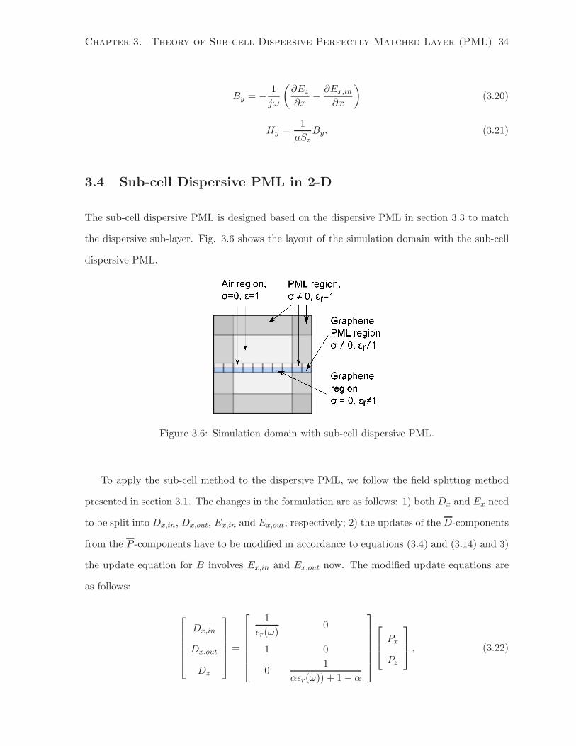
The sub-cell dispersive PML is designed based on the dispersive PML in section 3.3 to match
the dispersive sub-layer. Fig. 3.6 shows the layout of the simulation domain with the sub-cell
dispersive PML.
Figure 3.6: Simulation domain with sub-cell dispersive PML.
To apply the sub-cell method to the dispersive PML, we follow the field splitting method
presented in section 3.1. The changes in the formulation are as follows: 1) both Dx and Ex need
to be split into Dx,in, Dx,out, Ex,in and Ex,out, respectively; 2) the updates of the D-components
from the P -components have to be modified in accordance to equations (3.4) and (3.14) and 3)
the update equation for B involves Ex,in and Ex,out now. The modified update equations are
as follows:
Dx,in
Dx,out
Dz
=
1
ǫr(ω)0
1 0
01
αǫr(ω)) + 1− α
Px
Pz
, (3.22)

Chapter 3. Theory of Sub-cell Dispersive Perfectly Matched Layer (PML) 35
Ex,in
Ex,out
Ez
=
1
ǫ0Sx 0 0
01
ǫ0Sx 0
0 01
ǫ0Sz
Dx,in
Dx,out
Dz
, (3.23)
By = − 1
jω
(
∂Ez
∂x− α
∂Ex,in
∂x− (1− α)
∂Ex,out
∂x
)
. (3.24)
To model graphene, replace ǫr(ω) in equation (3.22) with the relative permittivity of graphene
in equation (3.25).
ǫr(ω) = 1 +Q
jωǫ0(jω + 2γ)= 1 +
Q/ǫ0−ω2 + 2γjω
(3.25)
The discretization of Dx,in is trivial since ǫr = 1 in this case:
Dn+1x,out = Pn+1
x . (3.26)
The update equation for Dx,in is as follows:
ǫr(ω)Dx,in = Px, (3.27)
(
1 +Q/ǫ0
(jω)2 + jω2γ
)
Dx,in = Px, (3.28)
jω(jω + 2γ)Px = jω(jω + 2γ)Dx,in +Q
ǫ0Dx,in. (3.29)
Converting the expression from frequency domain to time domain via jω → ∂∂t :
∂2
∂t2Px +
∂
∂t(2γ)Px =
∂2
∂t2Dx,in +
∂
∂t(2γ)Dx,in +
Q
ǫ0Dx,in. (3.30)
The discretization in time domain is as follows:
Pn+1x − 2Pn
x + Pn−1x
∆t2+ 2γ
Pn+1x − Pn−1
x
2∆t=
Dn+1x,in − 2Dn
x,in +Dn−1x,in
∆t2
+ 2γDn+1
x,in −Dn−1x,in
2∆t+
Q
ǫ0
Dn+1x,in + 2Dn
x,in +Dn−1x,in
4.
(3.31)
Center averaging is used for discretizing each term. Notice that Dn has been discretized as
Chapter 3. Theory of Sub-cell Dispersive Perfectly Matched Layer (PML) 36
Dn+1
x,in+2Dnx,in+Dn−1
x,in
4 for improved stability as mentioned in [35]. The final update equation for
Dx,in is:
Dn+1x,in =
(
Q∆t2
2ǫ0− 2
)
Dnx,in −
(
1− γ∆t+Q∆t2
4ǫ0
)
Dn−1x,in
+(1 + γ∆t)Pn+1x − 2Pn
x + (1− γ∆t)Pn−1x
/
1 + γ∆t+Q∆t2
4ǫ0
.
(3.32)
Similar approach can be applied to find the update equation for Dz:
(αǫr(ω) + 1− α)Dz = Pz, (3.33)
and
αǫr(ω) + 1− α = α+αQ/ǫ0
(jω)2 + jω2γ+ 1− α = 1 +
αQ/ǫ0(jω)2 + jω2γ
. (3.34)
Comparing equation (3.34) with equation (3.25), the only difference is the extra α factor ap-
pearing in front of Q in equation (3.34) that does not present in equation (3.25). Following the
same discretization, the update equation for Dz is as follows:
Dn+1z =
(
αQ∆t2
2ǫ0− 2
)
Dnz −
(
1− γ∆t+αQ∆t2
4ǫ0
)
Dn−1z
+(1 + γ∆t)Pn+1z − 2Pn
z + (1− γ∆t)Pn−1z
/
1 + γ∆t+αQ∆t2
4ǫ0
.
(3.35)
To complete the set, the other update equations are shown below:
Pn+1x =
1− ∆tσz,i+0.5,j
2ǫ0
1 +∆tσz,i+0.5,j
2ǫ0
Pnx − ∆t∆x
∆z(1 +∆tσz,i+0.5,j
2ǫ0)(Hn+0.5
y,i+0.5,j+0.5 −Hn+0.5y,i+0.5,j−0.5) (3.36)
Pn+1z =
1− ∆tσx,i+0.5,j
2ǫ0
1 +∆tσx,i+0.5,j
2ǫ0
Pnz +
∆t∆z
∆x(1 +∆tσx,i+0.5,j
2ǫ0)(Hn+0.5
y,i+0.5,j+0.5 −Hn+0.5y,i−0.5,j+0.5) (3.37)
En+1x,in = En
x,in +1
ǫ0((1 +
∆tσx,i+0.5,j
2ǫ0)Dn+1
x,in − (1− ∆tσx,i+0.5,j
2ǫ0)Dn
x,in) (3.38)
Chapter 3. Theory of Sub-cell Dispersive Perfectly Matched Layer (PML) 37
En+1x,out = En
x,out +1
ǫ0((1 +
∆tσx,i+0.5,j
2ǫ0)Dn+1
x,out − (1− ∆tσx,i+0.5,j
2ǫ0)Dn
x,out) (3.39)
En+1z = En
z +1
ǫ0((1 +
∆tσz,i+0.5,j
2ǫ0)Dn+1
z − (1− ∆tσz,i+0.5,j
2ǫ0)Dn
z ) (3.40)
Bn+0.5y,i+0.5,j+0.5 =
1− ∆tσx,i+0.5,j
2ǫ0
1 +∆tσx,i+0.5,j
2ǫ0
Bn−0.5y,i+0.5,j+0.5 +
∆t
∆z∆x(1 +∆tσx,i+0.5,j
2ǫ0)(En
z,i+1,j − Enz,i,j
− Enx,i,j+1 + En
x,i,j)
(3.41)
Hn+0.5y,i+0.5,j+0.5 =
1− ∆tσz,i+0.5,j
2ǫ0
1 +∆tσz,i+0.5,j
2ǫ0
Hn−0.5y,i+0.5,j+0.5 +
1
µ0(1 +∆tσx,i+0.5,j
2ǫ0)(Bn+0.5
y,i+0.5,j+0.5 −Bn−0.5y,i+0.5,j+0.5).
(3.42)
Equations (3.26),(3.32),(3.35) and equations (3.36) - (3.42) form a complete set of update
equations for the 2-D sub-cell dispersive PML.
3.5 Sub-cell Dispersive PML in 3-D
The 3-D sub-cell dispersive PML can be derived in the same way as the 2-D scheme developed
in section 3.4. The derivation process is skipped and the update equations in differential form
are presented below:
Px
Py
Pz
=1
jω
1
Sy0 0
01
Sz0
0 01
Sx
∂Hz
∂y− ∂Hy
∂z∂Hx
∂z− ∂Hz
∂x∂Hy
∂x− ∂Hx
∂y
(3.43)
Dx,in
Dx,out
Dy
Dz
=
1
ǫr(ω)0 0
1 0 0
01
αǫr(ω) + 1− α0
0 01
αǫr(ω) + 1− α
Px
Py
Pz
(3.44)

Chapter 3. Theory of Sub-cell Dispersive Perfectly Matched Layer (PML) 38
Ex,in
Ex,out
Ey
Ez
=
1
ǫ0
Sx
Sz0 0 0
01
ǫ0
Sx
Sz0 0
0 01
ǫ0
Sy
Sx0
0 0 01
ǫ0
Sz
Sy
Dx,in
Dx,out
Dy
Dz
(3.45)
Bx
By
Bz
= − 1
jω
1
Sy0 0
01
Sz0
0 01
Sx
0 0 − ∂
∂z
∂
∂y
α∂
∂z(1− α)
∂
∂z0 − ∂
∂x
−α∂
∂y−(1− α)
∂
∂y
∂
∂x0
Ex,in
Ex,out
Ey
Ez
(3.46)
Hx
Hy
Hz
=1
µ0
Sx
Sz0 0
0Sy
Sx0
0 0Sz
Sy
Bx
By
Bz
. (3.47)
Equations (3.43) - (3.47) form a complete set of update equations for the 3-D sub-cell
dispersive PML.
3.6 Summary
In this chapter, the sub-cell technique has been introduced and applied to model graphene.
Using the sub-cell technique to model graphene allows the spatial cell size to be larger than
the smallest physical feature (thickness) of graphene, thereby reducing both the memory re-
quirement and the simulation time. The 2-D sub-cell FDTD update equations for graphene
have been derived first, and the dispersive PML has been integrated into the sub-cell FDTD
scheme and the resulting update equations have been presented. The sub-cell dispersive PML
can be used to terminate infinite structures such as waveguides that have graphene sub-layers
extended into the PML. The framework has been extended to 3-D to allow applications with
more complicated geometries to be studied.

Chapter 4
Numerical Results for Sub-cell PML
The sub-cell dispersive PML framework developed in Chapter 3 is validated in this chapter.
The PML error studies characterize the performance of the sub-cell PML. Several test cases of
dielectrics and graphene structures further demonstrate the functionality and accuracy of the
sub-cell PML framework.
4.1 Study of PML Parameters
To study the performance of the PML, a test designed to optimize the PML parameters [36]
is performed on the graphene PML. Two parameters are studied: the PML polynomial grade
number (m), as defined in σx(x) = (x/d)mσx,max, is varied within the range of 1 ≤ m ≤ 6 with
a 0.1 increment and the σmax value is varied between 0.1 × σopt to 4 × σopt, with a 0.1 × σopt
increment, where
σopt = −(m+ 1)(−16)
2ηd(4.1)
as defined in [34] for general UPML, with η = 120π and d = 50 ×∆z being the width of the
PML region.
The simulation domain is 160 × 160 cells, with a 50 cell PML on each side of the 2-D TMz
domain as shown in Fig. 4.1. The grid is 7.5µm and dt = 1.6794 × 10⁻¹⁴, which corresponds
to SlL = 0.95× CFL limit. The test is run for 20000 steps, because it takes a long time for
the entire waveform to reach probe B, due to the highly dispersive nature of graphene. The
39
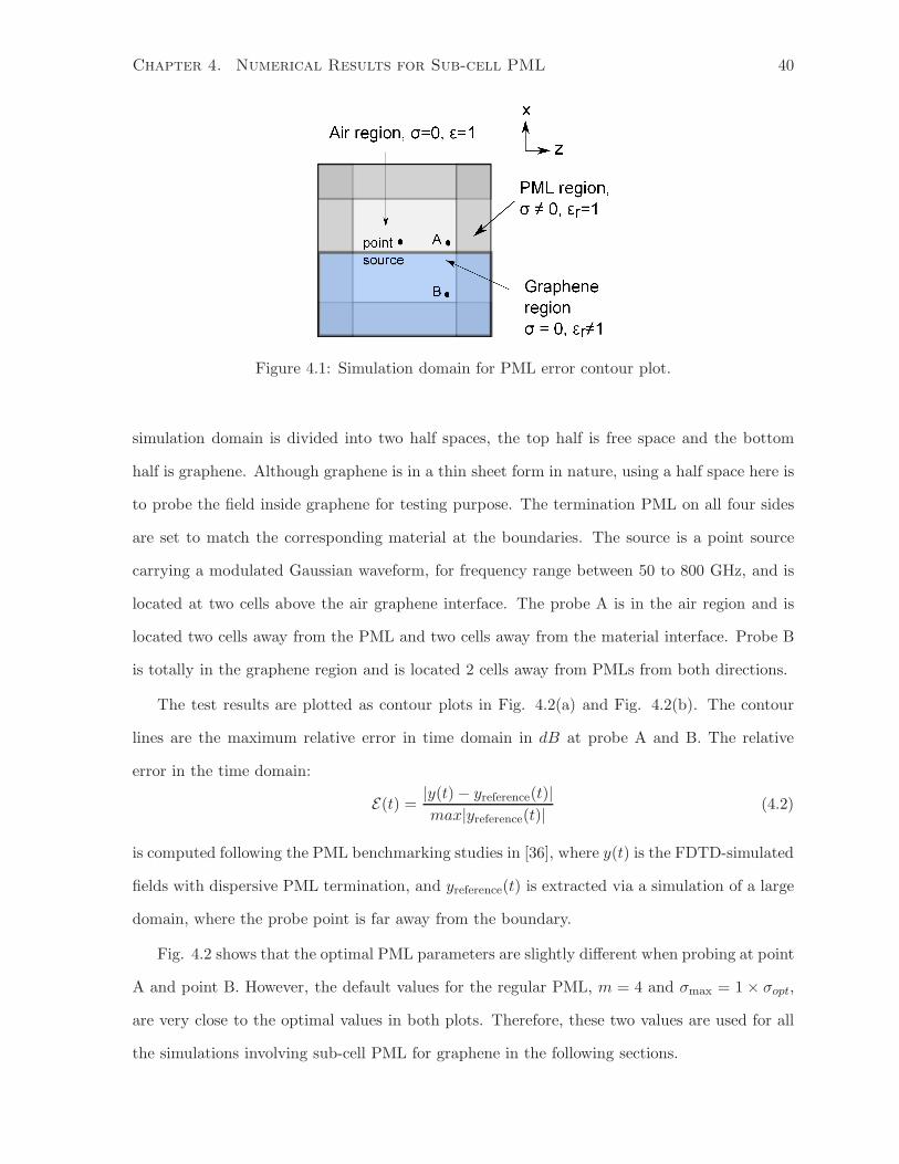
Chapter 4. Numerical Results for Sub-cell PML 40
Figure 4.1: Simulation domain for PML error contour plot.
simulation domain is divided into two half spaces, the top half is free space and the bottom
half is graphene. Although graphene is in a thin sheet form in nature, using a half space here is
to probe the field inside graphene for testing purpose. The termination PML on all four sides
are set to match the corresponding material at the boundaries. The source is a point source
carrying a modulated Gaussian waveform, for frequency range between 50 to 800 GHz, and is
located at two cells above the air graphene interface. The probe A is in the air region and is
located two cells away from the PML and two cells away from the material interface. Probe B
is totally in the graphene region and is located 2 cells away from PMLs from both directions.
The test results are plotted as contour plots in Fig. 4.2(a) and Fig. 4.2(b). The contour
lines are the maximum relative error in time domain in dB at probe A and B. The relative
error in the time domain:
E(t) = |y(t)− yreference(t)|max|yreference(t)|
(4.2)
is computed following the PML benchmarking studies in [36], where y(t) is the FDTD-simulated
fields with dispersive PML termination, and yreference(t) is extracted via a simulation of a large
domain, where the probe point is far away from the boundary.
Fig. 4.2 shows that the optimal PML parameters are slightly different when probing at point
A and point B. However, the default values for the regular PML, m = 4 and σmax = 1 × σopt,
are very close to the optimal values in both plots. Therefore, these two values are used for all
the simulations involving sub-cell PML for graphene in the following sections.

Chapter 4. Numerical Results for Sub-cell PML 41
σmax
/ σopt
m
0.5 1 1.5 2 2.5 3 3.5 41
1.5
2
2.5
3
3.5
4
4.5
5
5.5
6
−130
−120
−110
−100
−90
−80
−70
−60
−50
−40
−30
−20
(a)
σmax
/ σopt
m
0.5 1 1.5 2 2.5 3 3.5 41
1.5
2
2.5
3
3.5
4
4.5
5
5.5
6
−90
−80
−70
−60
−50
−40
−30
−20
(b)
Figure 4.2: Contour plot for graphene PML error in dB (a) at point A (b) at point B.

Chapter 4. Numerical Results for Sub-cell PML 42
4.2 Sub-cell PML Error Test with Dielectric Slab Structure
As an initial test for the time domain reflection error in sub-cell PML, a stack of three sub-cell
layers terminated into a PML is studied. The test is on a dielectric structure because it is
easier to quantify the performance of the sub-cell PML and compare to the air PML on such
structures. The parallel dielectric layers of ǫr = 12 are modeled with sub-cell PML framework
as shown in Fig. 4.3. The layers are separated by 75 µm in the x-direction and terminated by
sub-cell PML in the z-direction.
Figure 4.3: Geometry of the three dielectric layer test structure terminated into a sub-cell PMLindicating the position of the field probe.
The PML region has 50− cells in the x−direction and 16 or 25 cells in the z-direction. The
main simulation domain is 100× 800 cells. The cell size is 7.5µm in both the x− and the z−
direction, which is λmin/50 and ∆t = 1.6794 × 10⁻¹⁴ which corresponds to SCFL = 0.95 times
the FDTD stability limit and 8192 steps are run. Moreover, a second simulation is performed
using a 16 or 25 cells air PML, ignoring the inserted sub-cell dielectric layer, to measure the
impact of the sub-cell layer on the overall performance of the absorber. The source for all tests
is a point source carrying a modulated Gaussian waveform, for frequency range between 50 to
800 GHz. It is located in the air region above all three dielectric plates, as shown in Fig. 4.3.
Field data are recorded at point A, which is located two cells away from the PML and two cells
away from the third layer, in the air region. The relative error in the time domain is calculated
with equation (4.2).

Chapter 4. Numerical Results for Sub-cell PML 43
200 400 600 800 1000 1200 1400 1600−150
−100
−50
0E
rror
(dB
)
16−cell sub−cell PML 16−cell regular PML
200 400 600 800 1000 1200 1400 1600−150
−100
−50
0
Time steps
Err
or (
dB)
25−cell sub−cell PML 25−cell regular PML
(a)
200 400 600 800 1000 1200 1400 1600−150
−100
−50
0
Err
or (
dB)
16−cell sub−cell PML 16−cell regular PML
200 400 600 800 1000 1200 1400 1600−150
−100
−50
0
Time steps
Err
or (
dB)
25−cell sub−cell PML 25−cell regular PML
(b)
Figure 4.4: Error of sub-cell PML in time domain for (a) α = 0.5 (b) α = 0.1.

Chapter 4. Numerical Results for Sub-cell PML 44
The relative error of the sub-cell PML is shown in Fig. 4.4. The maximum relative error
occurs within the first 1600 time steps. For the α = 0.5 case, the maximum error for the air
PML case goes up to -18 dB, whereas with the sub-cell PML in place, the maximum error
reduces to -51 dB for the 16-cell sub-cell PML. Similarly, for the α = 0.1 case, the maximum
error for the sub-cell PML is -57 dB for the 16-cell sub-cell PML, compared to -46 dB of the
air PML. Error is further reduced when 25-cell PML is in place. A few points to be made with
the results are as follows. First, the errors for all cases with α = 0.1 are smaller than those for
α = 0.5 because when α = 0.1, the inserted sub-layer is thinner, hence a smaller area is covered
by the dielectric-PML interface. Second, the error for the regular PML increases significantly
with the dielectric contrast between the thin layer and the surrounding medium. While the air
PML still provides a poor matching condition for the dielectric layers, no meaningful result can
be obtained with the air PML for a graphene sub-layer like the example in section 4.5.
For the above structure with the dielectric layer modeled by an α = 0.1 sub-cell, the run
time of the simulation for 8192 steps is 391s in comparison to a run time of 5383s using a regular
FDTD mesh; while ∆z = 7.5µm for both tests. The sub-cell method reduces the execution
time by more than 10 times, because for the same size of simulation domain, the number of
cells is reduced by a factor of 10 when using a sub-cell method at α = 0.1. Also, substantially
less memory is required when the sub-cell method is applied.
4.3 Dielectric Slab Transmission Coefficient Test
A dielectric slab structure as shown in Fig. 4.5 is simulated using the same parameters as the
test case in section 4.2, to show the accuracy of the sub-cell framework on dielectric structures.
The sub-cell PML has 10 cells in the x direction and 25 cells in the z direction. A sub-cell
α = 0.5 is used in this simulation.
4.3.1 Theoretical Solution
The analytical transmission coefficient for a dielectric slab in the air is found as follows:
First, find the impedance at the interface of first 2 slabs, at z = 0, as in Fig. 4.6:
Z2(0) = η2η1 cos(β2d) + jη2 sin(β2d)
η2 cos(β2d) + jη1 sin(β2d), (4.3)

Chapter 4. Numerical Results for Sub-cell PML 45
Figure 4.5: Computational domain for plane wave incidence on a dielectric slab.
z=0 z=d
ε1 ε1
z
ε2
Figure 4.6: Geometry of a 3-slab structure.
where material 1 is the air and material 2 is the dielectric with ǫr = 12. In equation (4.3)
β2 = ω√ǫr√
(µ0ǫ0) and d is the thickness of the dielectric layer.
Then, the reflection coefficient and transmission coefficient can be found as:
Γ =Z2(0) − η0Z2(0) + η0
, (4.4)
T = 1 + Γ. (4.5)
4.3.2 Simulation Results
The transmission coefficient for the dielectric slab from the simulation is shown in Fig. 4.7.
It is clear that the simulation result matches very well with the analytical solution, for both
the magnitude and the phase. A reference case where the dielectric structure terminated with
a regular air PML is run, and the result is shown in Fig. 4.8. The discrepancy between the
simulation result and the analytical solution shows that even when the value of ǫr is small, the
sub-cell PML is needed to get an accurate simulation result.
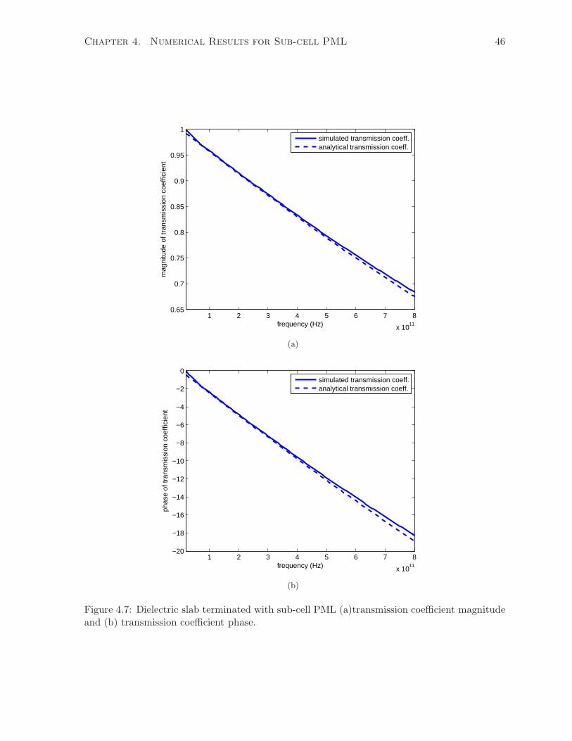
Chapter 4. Numerical Results for Sub-cell PML 46
1 2 3 4 5 6 7 8
x 1011
0.65
0.7
0.75
0.8
0.85
0.9
0.95
1
frequency (Hz)
mag
nitu
de o
f tra
nsm
issi
on c
oeffi
cien
t
simulated transmission coeff.analytical transmission coeff.
(a)
1 2 3 4 5 6 7 8
x 1011
−20
−18
−16
−14
−12
−10
−8
−6
−4
−2
0
frequency (Hz)
phas
e of
tran
smis
sion
coe
ffici
ent
simulated transmission coeff.analytical transmission coeff.
(b)
Figure 4.7: Dielectric slab terminated with sub-cell PML (a)transmission coefficient magnitudeand (b) transmission coefficient phase.

Chapter 4. Numerical Results for Sub-cell PML 47
1 2 3 4 5 6 7 8
x 1011
0.65
0.7
0.75
0.8
0.85
0.9
0.95
1
frequency (Hz)
mag
nitu
de o
f tra
nsm
issi
on c
oeffi
cien
t
simulated transmission coeff.analytical transmission coeff.
(a)
1 2 3 4 5 6 7 8
x 1011
−20
−15
−10
−5
0
5
frequency (Hz)
phas
e of
tran
smis
sion
coe
ffici
ent
simulated transmission coeff.analytical transmission coeff.
(b)
Figure 4.8: Dielectric slab terminated with regular air PML (a)transmission coefficient magni-tude and (b) transmission coefficient phase.
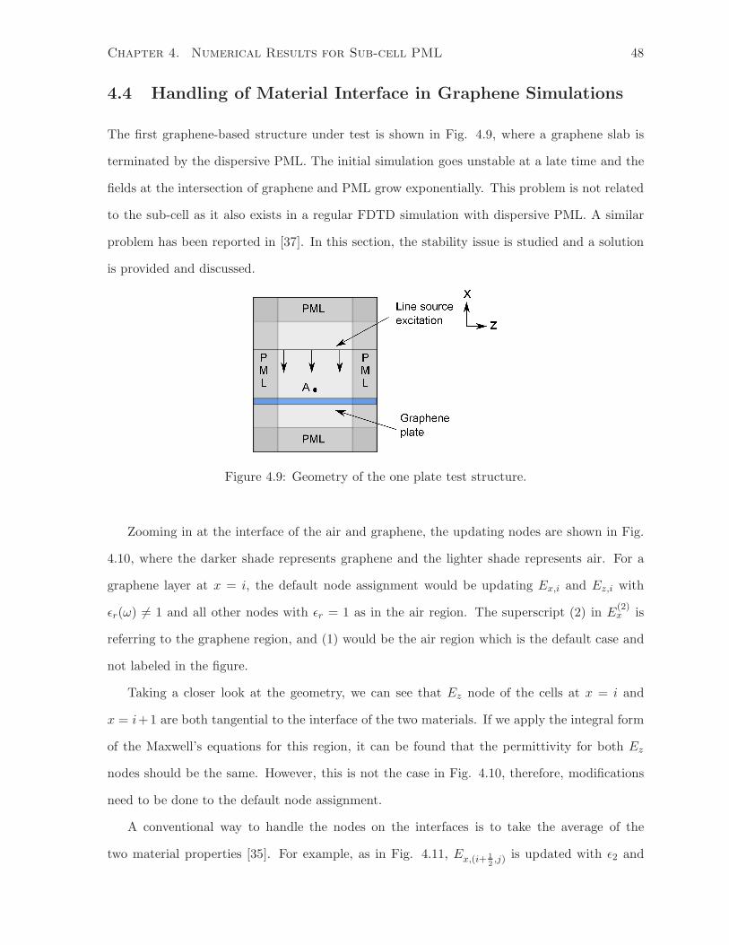
Chapter 4. Numerical Results for Sub-cell PML 48
4.4 Handling of Material Interface in Graphene Simulations
The first graphene-based structure under test is shown in Fig. 4.9, where a graphene slab is
terminated by the dispersive PML. The initial simulation goes unstable at a late time and the
fields at the intersection of graphene and PML grow exponentially. This problem is not related
to the sub-cell as it also exists in a regular FDTD simulation with dispersive PML. A similar
problem has been reported in [37]. In this section, the stability issue is studied and a solution
is provided and discussed.
Figure 4.9: Geometry of the one plate test structure.
Zooming in at the interface of the air and graphene, the updating nodes are shown in Fig.
4.10, where the darker shade represents graphene and the lighter shade represents air. For a
graphene layer at x = i, the default node assignment would be updating Ex,i and Ez,i with
ǫr(ω) 6= 1 and all other nodes with ǫr = 1 as in the air region. The superscript (2) in E(2)x is
referring to the graphene region, and (1) would be the air region which is the default case and
not labeled in the figure.
Taking a closer look at the geometry, we can see that Ez node of the cells at x = i and
x = i+1 are both tangential to the interface of the two materials. If we apply the integral form
of the Maxwell’s equations for this region, it can be found that the permittivity for both Ez
nodes should be the same. However, this is not the case in Fig. 4.10, therefore, modifications
need to be done to the default node assignment.
A conventional way to handle the nodes on the interfaces is to take the average of the
two material properties [35]. For example, as in Fig. 4.11, Ex,(i+ 1
2,j) is updated with ǫ2 and
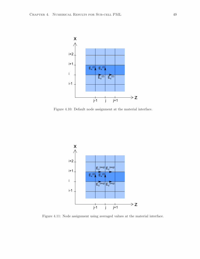
Chapter 4. Numerical Results for Sub-cell PML 49
x
z
i
i+1
i+2
i-1
j j+1j-1
Ex(2) Ex
(2)
Ez(2) Ez
(2)
Figure 4.10: Default node assignment at the material interface.
x
z
i
i+1
i+2
i-1
j j+1j-1
Ex(2) Ex
(2)
Ez(avg) Ez
(avg)
Ez(avg) Ez
(avg)
Figure 4.11: Node assignment using averaged values at the material interface.

Chapter 4. Numerical Results for Sub-cell PML 50
Ex,(i− 1
2,j) and Ex,(i+ 3
2,j) is updated with ǫ1, where ǫ1 is for air and ǫ2 is for graphene. Ez,(i,j+ 1
2)
and Ez,(i+1,j+ 1
2) are both updated with ǫavg = (ǫ1+ǫ2)
2 . However, when the averaging technique
is applied, the simulation still suffers from the late time instability. (Refer to Fig 4.15 (b).)
Looking into the node assignment for the averaging method, we find that there is a conflict
in updating the Ex node and the nearby Ez nodes, as illustrated in Fig. 4.12. To update the
Ex,(i+ 1
2,j) node by applying the Maxwell’s equations with ǫ = ǫ2, it is implying the graphene
layer is located between x = i and x = i+1 and has a relative permittivity of ǫ = ǫ2. However,
to update Ez,(i,j+ 1
2) and Ez,(i+1,j+ 1
2) with ǫ = ǫavg , it is implying the material between x = i− 1
2
and x = i+ 32 has a relative permittivity of ǫ = ǫavg. Assigning different ǫr values to the same
spatial region when updating Ex and Ez could potentially be the reason of having a late time
instability. This discrepancy does not raise a stability issue for the dielectric simulations because
the ǫr value is very small in dielectrics (order of 10) comparing to that of graphene or silver (in
the order of 107).
x
z
i
i+1
i+2
i-1
j j+1j-1
Ex(2) Ex
(2)
(a)
x
z
i
i+1
i+2
i-1
j j+1j-1
Ez(avg) Ez
(avg)
Ez(avg) Ez
(avg)
(b)
Figure 4.12: A conflicting node assignment for the averaging method (a) for updating Ex (b)for updating Ez.
In order to improve the stability condition and to maintain the accuracy level of the simu-
lation, a new node assignment scheme is proposed. As shown in Fig. 4.13, for a graphene layer
at x = i, Ex,(i+ 1
2,j) as well as both of Ez,(i,j+ 1
2) and Ez,(i+1,j+ 1
2) are updated using ǫ2. For the
cells at x = i + 1, the Ex,(i+ 3
2,j) node is assumed to be just above x = i + 3
2 and is entirely in
air. Hy,(i+ 3
2,j+ 1
2) is updated using Ez,(i+1,j+ 1
2) which is in the graphene and Ez,(i+2,j+ 1
2), which
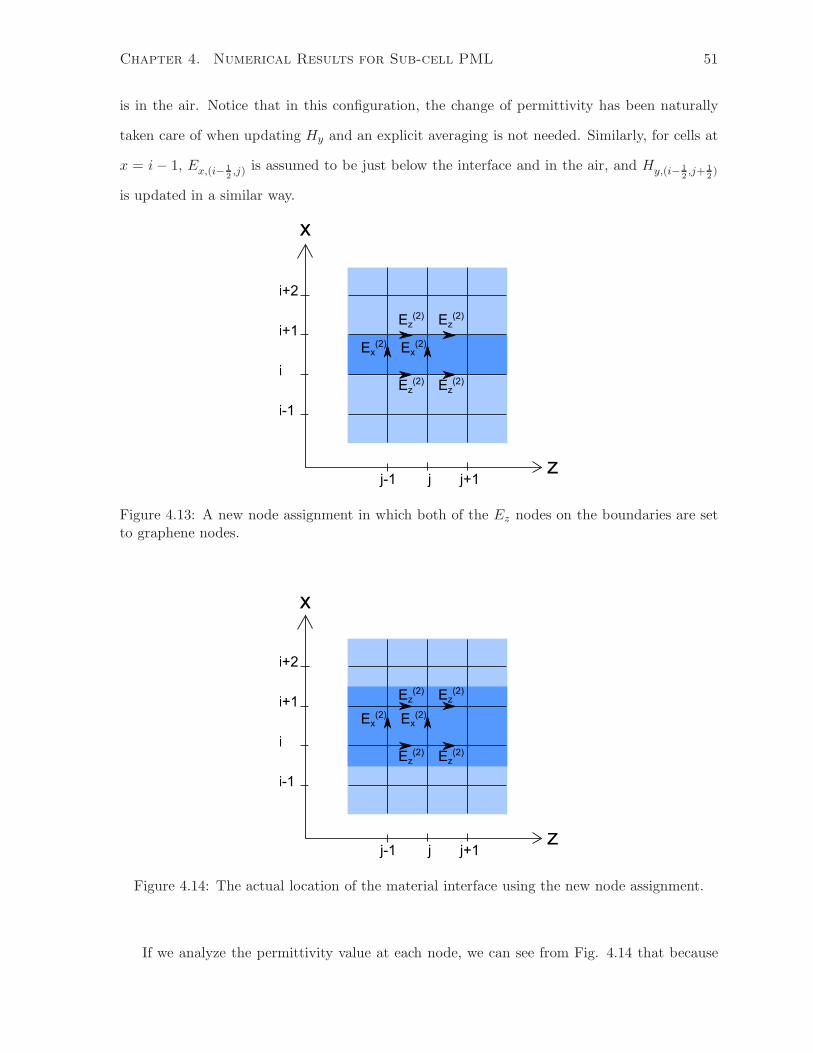
Chapter 4. Numerical Results for Sub-cell PML 51
is in the air. Notice that in this configuration, the change of permittivity has been naturally
taken care of when updating Hy and an explicit averaging is not needed. Similarly, for cells at
x = i− 1, Ex,(i− 1
2,j) is assumed to be just below the interface and in the air, and Hy,(i− 1
2,j+ 1
2)
is updated in a similar way.
x
z
i
i+1
i+2
i-1
j j+1j-1
Ex(2) Ex
(2)
Ez(2) Ez
(2)
Ez(2) Ez
(2)
Figure 4.13: A new node assignment in which both of the Ez nodes on the boundaries are setto graphene nodes.
x
z
i
i+1
i+2
i-1
j j+1j-1
Ex(2) Ex
(2)
Ez(2) Ez
(2)
Ez(2) Ez
(2)
Figure 4.14: The actual location of the material interface using the new node assignment.
If we analyze the permittivity value at each node, we can see from Fig. 4.14 that because

Chapter 4. Numerical Results for Sub-cell PML 52
both Ez,(i,j+ 1
2) and Ez,(i+1,j+ 1
2) are updated using ǫ2, essentially the region between x = i− 1
2
and x = i+ 32 is the graphene region, and the boundaries between air and graphene have been
pushed to x = i − 12 and x = i + 3
2 . With the shifting of boundaries in place, the effective
thickness of the graphene layer in the simulation is 2×∆x. It is important to know the exact
effective graphene layer thickness because it is involved in finding the volumetric graphene
conductivity.
0 1 2 3 4 5 6 7
x 104
−1
0
1
Regular node assignment
0 1 2 3 4 5 6 7
x 104
−1
0
1
Averaging permittivity at material boundary
0 1 2 3 4 5 6 7
x 104
−1
0
1
time steps
Ez
field
shift material interface by half grid at boundary
Figure 4.15: Comparison of late time stability conditions using different node assignments insimulations.
A comparison of late time stability performance is presented in Fig. 4.15. All three tests
are run with same parameters except the interface node handling. It is shown that with both
the regular node assignment and the averaging method, the simulations go unstable around 60k
time steps, and only the boundary shifting method remains stable in late time.
4.5 Graphene Slab Test in 2-D
After resolving the late time instability issue in section 4.4, the sub-cell dispersive PML frame-
work can be applied to simulate the graphene slab structure.

Chapter 4. Numerical Results for Sub-cell PML 53
4.5.1 Theoretical Solution
The analytical transmission coefficient for a lossy slab between air can be found in a similar
way as presented in section 4.3.1. Referring to Fig. 4.6, the impedance at the interface of first
2 slabs, at z = 0, is:
Z2(0) = η2η1 cosh(γ2d) + η2 sinh(γ2d)
η1 sinh(γ2d) + η2 × cosh(γ2d). (4.6)
Here, material 1 is air and material 2 is graphene. In equation (4.6) γ = jω√
(µǫ) = j ωc
√
(ǫr),
d is the thickness of graphene layer.
Then, the reflection coefficient and transmission coefficient can be found as:
Γ =Z2(0) − η0Z2(0) + η0
, (4.7)
T = 1 + Γ. (4.8)
4.5.2 Simulation Results
Figure 4.16: Computational domain for plane wave incidence on a graphene slab.
The geometry of the test structure is shown in Fig. 4.16. The graphene sheet is modeled as a
sub-cell layer in the x-direction. A line source excites the Ez field with a modulated Gaussian
pulse of 2 THz bandwidth, producing a plane wave incident normally onto the graphene sheet.
The spatial mesh is ∆x = ∆z = λmin/1000. The thickness of the graphene plate is d =
2× α×∆x = 3 nm, with α = 0.01. The parameters for graphene in this test are µc = 0.2 eV,
γ = 0.065 meV and T = 300 K as in [38].
To record the data, a probe is set at point A, which is one cell above the graphene sheet and

Chapter 4. Numerical Results for Sub-cell PML 54
500 1000 1500 20000.1
0.2
0.3
0.4
0.5
0.6
0.7
0.8
Frequency (GHz)
|S21
|
Simulated with Sub−cell PMLAnalytical Solution
500 1000 1500 2000
−4
−2
0
Simulated with regular PMLAnalytical Solution
(a)
400 600 800 1000 1200 1400 1600 1800 20000
10
20
30
40
50
60
70
80
Frequency (GHz)
∠ S
21 (
degr
ee)
Simulated with Sub−cell PMLAnalytical Solution
500 1000 1500 2000−400
−200
0
200
Simulated with regular PMLAnalytical Solution
(b)
Figure 4.17: (a)Transmission coefficient magnitude, inset: simulation with air PML and (b)transmission coefficient phase, inset: simulation with air PML.

Chapter 4. Numerical Results for Sub-cell PML 55
in the middle of the domain in the z− direction. The incident field is obtained from running a
simulation in the same domain without the graphene sub-layer and the reflected field is found
by subtraction of the incident field from the total field. Also, the transmission coefficient of
the slab is found analytically. The simulation results are compared with the analytical solution
and shown in Fig. 4.17.
From Fig. 4.17, it is clear that with the sub-cell scheme in place, both the magnitude
and phase of the transmission coefficient obtained from the simulation match well with the
analytical solution. This shows that the sub-cell PML scheme can provide accurate simulations
for graphene-based devices while reducing the simulation time and memory requirements. In
fact, the same simulation with a regular FDTD mesh is not even feasible due to an extremely
high computational cost. The inset of Fig. 4.17 shows the graphene transmission coefficient
simulated with the regular air PML in comparison to the analytical solution. The significant
discrepancies between the two solutions attest to the fact that the sub-cell PML is necessary
to properly terminate the graphene sub-layer.
4.6 Graphene Slab Test in 3-D
Figure 4.18: A 3-D computational domain for plane wave incidence on a graphene slab.
A similar graphene slab structure as in section 4.5 has been used to test the 3-D framework.
The structure is shown in Fig. 4.18. The graphene sheet is modeled as a sub-cell layer in

Chapter 4. Numerical Results for Sub-cell PML 56
the x-direction. Instead of using a line source, a plane of source excitation is located above
the graphene layer and produces a plane wave incident normally onto the graphene sheet. The
spatial mesh is ∆x = ∆y = ∆z = λmin/20 and α = 0.01. Although the thickness of the graphene
plate is not exact with this mesh, it serves the purpose of numerical demonstration, as using a
fine mesh in 3-D test requires a large memory and long simulation time. The parameters for
graphene in this test is µc = 0.2 eV, γ = 0.065 meV and T = 300 K as in [38] which is the same
as that of the 2-D simulation.
The simulation result is shown in Fig. 4.19. The analytical solution has been solved in
section 4.5 and not repeated here. The simulation result matches with the analytical solution
as in the case of 2-D simulation scheme, confirming the functionality and accuracy of the 3-D
scheme.
4.7 Graphene Parallel Plate Waveguide Test
Many graphene applications can be investigated using the sub-cell PML framework. One of the
applications of our interest is a 2-D parallel plate waveguide (PPWG) using graphene sheets
instead of metallic ones as the plates [27]. In this study, the dominant quasi-transverse electro-
magnetic (TEM) mode of the PPWG is excited and parameters such as the wave impedance,
propagation constant and attenuation constant of the waveguide are studied and compared to
the analytical solutions.
4.7.1 Theoretical Solution
Figure 4.20 shows the geometry of the graphene PPWG. It consists of two laterally infinite
graphene plates in the yz plane separated by a distance of 1000 nm in the x− direction. When
modeled in a 2-D domain, a cross-section of the waveguide in the xz plane is taken. This way it
is implicitly defined that the plates are infinite in the y− direction. The plates extend infinitely
in the z− direction, and they are terminated by the sub-cell PML in simulations.
In [27], the modal fields guided by the graphene PPWG in Fig. 4.20 have been studied

Chapter 4. Numerical Results for Sub-cell PML 57
500 1000 1500 20000.1
0.2
0.3
0.4
0.5
0.6
0.7
0.8
Frequency (GHz)
|S21
| (dB
)
Simulated with Sub−cell PMLAnalytical Solution
(a)
500 1000 1500 200015
20
25
30
35
40
45
50
55
Frequency (GHz)
∠ S
21 (
degr
ee)
Simulated with Sub−cell PMLAnalytical Solution
(b)
Figure 4.19: (a)Transmission coefficient magnitude, and (b) transmission coefficient phase.

Chapter 4. Numerical Results for Sub-cell PML 58
x
z
y
x
z
d
ε1
ε1
ε1
Figure 4.20: Geometry of the parallel plate waveguide.
analytically, and the wave constant for the quasi- TEM mode has been found as follows:
γ/k0 ≃√
1 +1
η20σ2
[
1− j2ση0k0d
]
. (4.9)
Following equation (4.9), the wave impedance can be found as:
Z = | Ex
η0Hy|= | γ
k0|. (4.10)
The propagation constant can be found as:
β = Re(γ), (4.11)
and the attenuation constant is:
α = 8.686Im(γ). (4.12)
4.7.2 Simulation Results
The simulation domain for the graphene PPWG study is shown in Fig. 4.21. The two graphene
plates are modeled with sub-layers with sub-cell αsub−cell = 0.1, and they are separated by 1000
nm. The spatical mesh is ∆ = 50 nm which is mainly limited by the geometry of the problem,
and ∆z = 500 nm. The source is a line source carrying a modulated Gaussian waveform, for
frequency range between 50 to 800 GHz, with Hy polarization. The fields are probed at two
spatial locations between the plates, with 1 cell separation in the z− direction between the two

Chapter 4. Numerical Results for Sub-cell PML 59
Figure 4.21: Computational domain for the graphene PPWG simulation.
probes.
The normalized wave impedance varies along the x direction, as shown in Fig. 4.22, in-
dicating the quasi-TEM wave being confined between the two plates. The normalized wave
impedance at f = 100 GHz and f = 800 GHz can be read from Fig. 4.22 and shows good
agreement with the analytical solution as presented in Table 4.1.
f=100 GHz f=800 GHz
Simulation (αsub−cell = 0.1) 9.45 5.434
Analytical solution 9.55 5.6
Table 4.1: Normalized wave impedance for the graphene parallel plate waveguide.
The normalized phase constant (β/k0) and attenuation constant (α) are plotted as a function
of frequency in Fig. 4.23 and Fig. 4.24. In both plots, the simulation results match with the
analytical solution very well.
In the PPWG test, a few sources of error are introduced when implementing the sub-cell
method to model the graphene thin layers: 1) The sub-cell αsub−cell introduces uncertainty
in the exact location of each plate in the x− direction, therefore the plate separation is not
exactly 1000 nm in the simulation. Comparing the simulation result of such structures with
the analytical solution that assumed 1000 nm plate separation, small error would show up;
2) Even with the sub-cell formulation, the modeled graphene thickness is not exactly 1 nm
in this case. Although this difference has been taken care of when calculating the volumetric

Chapter 4. Numerical Results for Sub-cell PML 60
−1 −0.5 0 0.5 10
5
10
15
x/d (the graphene planes lie at x=± d/2)
Ex/
η 0/Hy
f=100GHzf=800GHz
Figure 4.22: Normalized wave impedance at a cross section of the PPWG.
0 200 400 600 8004
6
8
10
12
14
16
Frequency (GHz)
beta
nor
mal
ized
(be
ta /
k0)
simulation resultanalytical solution
Figure 4.23: Normalized phase constant (β/k0) for graphene PPWG.

Chapter 4. Numerical Results for Sub-cell PML 61
0 200 400 600 8000
0.02
0.04
0.06
0.08
0.1
0.12
0.14
0.16
Frequency (GHz)
alph
a (d
B/m
icro
n)
simulation resultanalytical solution
Figure 4.24: Attenuation constant (α) for the graphene PPWG.
conductivity model for each case, and should not make a significant impact in the simulation
result as discussed in [23], it remains a source of error in this simulation.
In general the choice of the sub-cell αsub−cell is a trade off between the computational
cost and simulation accuracy. While it is desirable to use a smaller αsub−cell to reduce the
computational cost to a greater extent, the uncertainly in the geometry of the structure can
affect the accuracy of the results significantly. Therefore, in most studies, αsub−cell values
between 0.01 and 0.5 are chosen.
4.8 Summary
In this chapter, the sub-cell dispersive PML framework has been validated through a series of
tests. The PML parameters were optimize through constructing a PML contour plot and the
PML reflection error in time domain were found consistently below -50 dB, for various PML
widths and sub-cell α values. A stability issue was encountered when developing the dispersive
PML for graphene. It was found that the problem was caused by the E field nodes on the
interface of the graphene and the air. The issue was resolved by modifying the node assignment

Chapter 4. Numerical Results for Sub-cell PML 62
at the material interface. The simulation framework was then validated through a dielectric slab
test in 2-D and graphene slab tests in both 2-D and 3-D. In all cases, the transmission coefficients
found from the simulations matched well with the analytical solutions. Furthermore, a parallel
plate waveguide was simulated and both the wave impedance and wave number extracted from
the simulation matched with the analytical solutions. These tests validated the functionality
and accuracy of the newly developed framework.

Chapter 5
Study of Graphene Antennas in 2-D
Graphene antennas support Surface Plasmon Polaritons (SPP) modes, and this desirable feature
allows miniaturization of antenna to micrometer scale without operating the antenna in optical
frequency range. In this chapter, the graphene patch antenna introduced in [21] and [39] is
studied using the sub-cell scheme in a 2-D domain.
5.1 Analytical Model of A Graphene Patch Antenna
Graphene antennas attract much attention from the graphene research community in recent
years because it offers the possibility of miniaturizing the antenna size without going into
very high resonant frequencies. Downsizing classical metallic antennas to the micrometer scale
would result in resonant frequencies in optical frequency range. Transceiver systems at such
frequency spectrum are infeasible to implement due to high channel attenuation. Graphene,
on the other hand, supports transverse-magnetic (TM) SPP waves, which travel at speeds
around c/50. This feature allows graphene antennas of micrometer size to resonate in the
terahertz frequency range, where practical transceiver systems can be implemented, therefore,
gives graphene antennas advantage over their metallic counterparts.
A graphene patch antenna is shown in Fig. 5.1. The antenna has a length L, and width
W . It is illuminated by a plane wave normal to the patch length. The antenna is assumed
to operate at room temperature (T=300 K), with µc = 0 and γ = 5 × 10¹². The graphene
63

Chapter 5. Study of Graphene Antennas in 2-D 64
conductivity is plotted in Fig. 5.2 based on equations (2.2), (2.3), for a frequency range below
3 THz. Fig. 5.2 shows that in the frequency range of interest, the intra-band conductivity
dominates over the inter-band conductivity. Therefore, in the following work, only intra-band
conductivity is used to model graphene.
Figure 5.1: Schematic of a graphene based patch antenna.
0 0.5 1 1.5 2 2.5−4
−2
0
2
4
6x 10
−4
σ intr
a (S
)
Re(σ
intra) Im (σ
intra)
0 0.5 1 1.5 2 2.50
2
4
6
8x 10
−5
frequency (THz)
σ inte
r (S
)
Re(σinter
) Im(σinter
)
Figure 5.2: Graphene conductivity at T=300 K, µc = 0 and γ = 5× 10¹².
A free-standing graphene layer supports TM SPP waves, and the dispersion relation is given
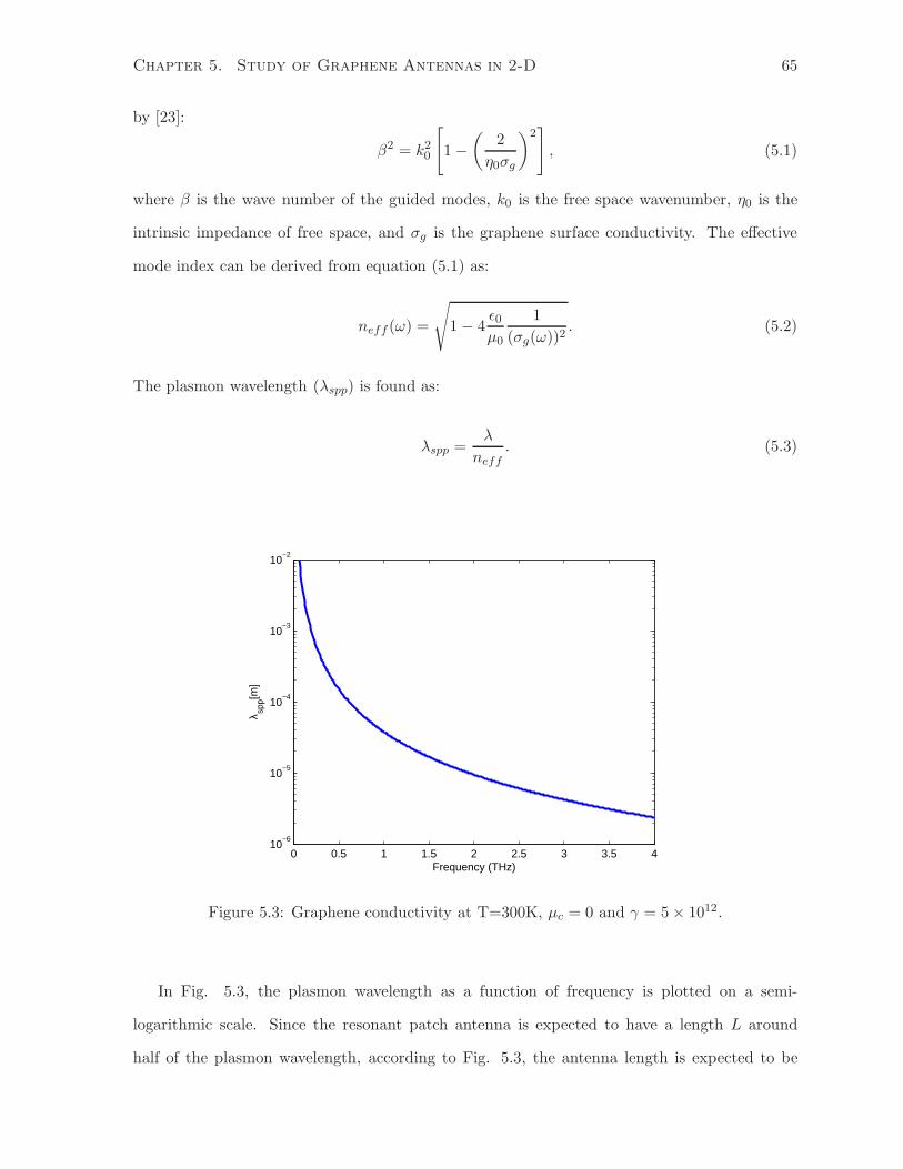
Chapter 5. Study of Graphene Antennas in 2-D 65
by [23]:
β2 = k20
[
1−(
2
η0σg
)2]
, (5.1)
where β is the wave number of the guided modes, k0 is the free space wavenumber, η0 is the
intrinsic impedance of free space, and σg is the graphene surface conductivity. The effective
mode index can be derived from equation (5.1) as:
neff (ω) =
√
1− 4ǫ0µ0
1
(σg(ω))2. (5.2)
The plasmon wavelength (λspp) is found as:
λspp =λ
neff. (5.3)
0 0.5 1 1.5 2 2.5 3 3.5 410
−6
10−5
10−4
10−3
10−2
Frequency (THz)
λ spp[m
]
Figure 5.3: Graphene conductivity at T=300K, µc = 0 and γ = 5× 10¹².
In Fig. 5.3, the plasmon wavelength as a function of frequency is plotted on a semi-
logarithmic scale. Since the resonant patch antenna is expected to have a length L around
half of the plasmon wavelength, according to Fig. 5.3, the antenna length is expected to be

Chapter 5. Study of Graphene Antennas in 2-D 66
on the order of a few micrometers in terahertz frequency range. The resonance condition for a
plasmonic patch antenna is [21]:
m1
2
λ
neff= L+ 2δL, (5.4)
where m is the order of the resonance, λ is the wavelength of incident wave, L is the antenna
length and δL is the field penetration length of the patch antenna. Equation (5.4) serves as a
guideline in designing graphene patch antennas.
5.2 Simulations of Graphene Patch Antennas in 2-D
Figure 5.4: Simulation domain for graphene patch antenna in 2-D.
Graphene patch antennas of various lengths L are simulated in a 2-D domain and their respective
resonant frequencies are found and compared to the analytical model. The 3-D graphene
antenna shown in Fig. 5.1 is in the yz plane with the thickness (t) of the graphene sheet in
the x− direction. When modeling the antenna in a 2-D domain, a cross section of the antenna
is taken in the xz plane, as shown in Fig. 5.4, and the width (W ) of the antenna is assumed
to be infinite in the y− direction. The length L is in the z− direction and the thickness t is
in the x− direction, which is modeled as a sub-cell layer. The spatial mesh is ∆x = 0.15µm
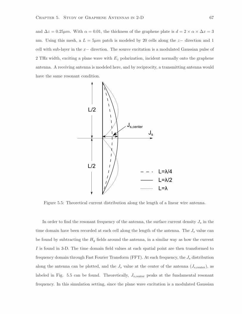
Chapter 5. Study of Graphene Antennas in 2-D 67
and ∆z = 0.25µm. With α = 0.01, the thickness of the graphene plate is d = 2× α×∆x = 3
nm. Using this mesh, a L = 5µm patch is modeled by 20 cells along the z− direction and 1
cell with sub-layer in the x− direction. The source excitation is a modulated Gaussian pulse of
2 THz width, exciting a plane wave with Ez polarization, incident normally onto the graphene
antenna. A receiving antenna is modeled here, and by reciprocity, a transmitting antenna would
have the same resonant condition.
L/2
L/2
Js
Js,center
L=λ/4
L=λ/2
L=λ
Figure 5.5: Theoretical current distribution along the length of a linear wire antenna.
In order to find the resonant frequency of the antenna, the surface current density Js in the
time domain have been recorded at each cell along the length of the antenna. The Js value can
be found by subtracting the Hy fields around the antenna, in a similar way as how the current
I is found in 3-D. The time domain field values at each spatial point are then transformed to
frequency domain through Fast Fourier Transform (FFT). At each frequency, the Js distribution
along the antenna can be plotted, and the Js value at the center of the antenna (Js,center), as
labeled in Fig. 5.5 can be found. Theoretically, Js,center peaks at the fundamental resonant
frequency. In this simulation setting, since the plane wave excitation is a modulated Gaussian
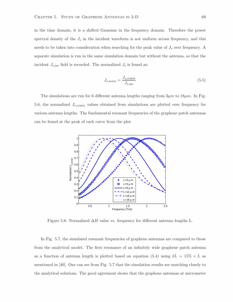
Chapter 5. Study of Graphene Antennas in 2-D 68
in the time domain, it is a shifted Gaussian in the frequency domain. Therefore the power
spectral density of the Js in the incident waveform is not uniform across frequency, and this
needs to be taken into consideration when searching for the peak value of Js over frequency. A
separate simulation is run in the same simulation domain but without the antenna, so that the
incident Js,inc field is recorded. The normalized Js is found as:
Js,norm =Js,centerJs,inc
(5.5)
The simulations are run for 6 different antenna lengths ranging from 3µm to 18µm. In Fig.
5.6, the normalized Js,center values obtained from simulations are plotted over frequency for
various antenna lengths. The fundamental resonant frequencies of the graphene patch antennas
can be found at the peak of each curve from the plot.
0.5 1 1.5 2 2.50
0.1
0.2
0.3
0.4
0.5
0.6
0.7
0.8
0.9
1
Frequency (THz)
Nor
mal
ized
Js,
cent
er
L=3 µ m
L=5 µ m
L=8 µ m
L=12 µ m
L=16 µ m
L=18 µ m
Figure 5.6: Normalized ∆H value vs. frequency for different antenna lengths L.
In Fig. 5.7, the simulated resonant frequencies of graphene antennas are compared to those
from the analytical model. The first resonance of an infinitely wide graphene patch antenna
as a function of antenna length is plotted based on equation (5.4) using δL = 15% × L as
mentioned in [40]. One can see from Fig. 5.7 that the simulation results are matching closely to
the analytical solutions. The good agreement shows that the graphene antennas at micrometer

Chapter 5. Study of Graphene Antennas in 2-D 69
0 5 10 15 200.5
1
1.5
2
2.5
3
Resonator Length (µ m)
Fre
quen
cy (
TH
z)
Analytical modelSimulation results
Figure 5.7: First resonance of an infinitely wide graphene patch antenna as a function of antennalength.
scale resonate in terahertz range as predicted by the analytical model.
5.3 Summary
In this chapter, a graphene patch antenna has been studied. The theory of the SPP mode
supported on the graphene sheet and the resonant condition for the graphene antenna have
been presented. Simulations of graphene patch antennas of various lengths in the micrometer
scale have been run in a 2-D domain. The first resonant frequencies found from the simulations
are in the terahertz range, consistent with the prediction from the analytical model. The free-
standing graphene patch antenna in 2-D is a simplified model of a 3-D patch antenna with a
finite width. The results in 2-D simulations show that graphene antennas have the potential to
be used as terahertz antennas. Further studies of the antenna parameters such as the antenna
width and substrate material or size can be carried out to fine tune the antenna resonant
frequency.

Chapter 6
Conclusion
6.1 Summary
With growing interest in the newly discovered 2-D material graphene, many applications have
been developed and EM simulation tools for graphene based devices would be necessary to
study the complicated devices where analytical solutions do not exist. This thesis focuses on
developing a simulation framework for modeling graphene based devices in the time domain
using the FDTD method.
A systematic approach has been applied to develop the simulation framework. Firstly, a
study of the various forms of the graphene conductivity model has been done. The graphene
conductivity can be represented as a sum of two parts: the intra-band conductivity and the
inter-band conductivity, and it is found that in the microwave frequency range, only the intra-
band conductivity is needed in the model. The FDTD update equations for modeling graphene
have been derived using the auxiliary differential equation (ADE) method. The dispersion and
stability study for the intra-band model have been performed and the stability condition for
the graphene update equations is found to be the CFL limit. The modeling of the inter-band
conductivity has been briefly discussed, a linear model is sufficient for the microwave frequency
range, and a piecewise linear model or a Pade approximation can be used for a wider frequency
range.
To develop a framework for simulating graphene based structures, a 2-D sub-cell scheme has
70
Chapter 6. Conclusion 71
been studied. The need for having the PML as the terminating boundary condition is rather
natural, since many waveguiding applications are infinite structures that need to be terminated
by PML in simulations. The dispersive PML for graphene has been developed and integrated
with the sub-cell scheme to form a sub-cell dispersive PML framework in 2-D and 3-D.
The newly developed sub-cell dispersive PML framework has been characterized and val-
idated on several cases. First of all, the time domain reflection error of the sub-cell PML is
found significantly lower than that of the air PML. Secondly, the transmission coefficient tests
for a dielectric slab in 2-D and graphene slabs in 2-D and 3-D are carried out and the simu-
lation results and analytical solutions show good agreement. In addition, a 2-D parallel plate
waveguide is characterized with the simulation framework, and both the wave impedance and
wave number are found to match with the analytical solution.
Following the validation of the framework, a graphene patch antenna is studied in a 2-
D domain. A free-standing graphene sheet supports TM SPP wave, which allows graphene
antennas of micrometer size to resonant at terahertz frequency. Graphene patch antennas of
lengths ranging from 3µm to 18µm have been simulated and their resonant frequencies are
found to be in the terahertz frequencies and match well with the analytical model based on the
SPP wavelength. Such results show that the graphene antenna is a good candidate for terahertz
applications.
6.2 Contributions
There are two major contributions resulted from this thesis:
Journal Publication:
X. Yu, C. D. Sarris, “A Perfectly Matched Layer for Sub-cell FDTD and Applications to the
Modeling of Graphene Structures”, IEEE Antennas and Wireless Propagation Letters, Vol. 11,
p1080-p1083, 2012
Conference Proceeding:
X. Yu, C. D. Sarris, “FDTD Modeling of Graphene-Based RF Devices: Fundamental Aspects
and Applications” Antennas and Propagation (APS/URSI), 2012 IEEE International Sympo-

Chapter 6. Conclusion 72
sium on, 8-14 July 2012
6.3 Future Work
The sub-cell dispersive PML framework has been proven working in both 2-D and 3-D, and it
forms a foundation for future studies on more graphene based applications. Here are some of
the possible extensions of this thesis:
Based on the existing framework, graphene patch antennas with finite width can be sim-
ulated and the resonant frequencies for different antenna widths can be compared. Other
applications such as the graphene coplanar waveguide in [17] and graphene microstrips can also
be characterized with the 3-D code.
Beside using the sub-cell scheme to model graphene, the surface impedance boundary condi-
tion (SIBC) [41], [42] can also be applied to model graphene. The SIBC method further relaxes
the constraint on the unit cell size comparing to the sub-cell method, because with SIBC, the
unit cell size is not limited by the smallest physical feature of the structure. However, as a
trade off, SIBC is more complicated to implement. Also, modification to the original SIBC
formulation is needed, if the graphene sheet is not located at the boundary but in the middle
of the simulation domain, as in the case of the parallel plate waveguide studied in section 4.7.
In order to extend the existing framework to model devices up to optical frequency, the inter-
band conductivity need to be taken into consideration. This can be done by applying the Pade
approximation for graphene inter-band conductivity from [32], as mentioned in Chapter 2. For
devices operating at the high terahertz frequency range, where the intra-band conductivity and
the inter-band conductivity have comparable magnitudes, both models are needed for accurate
simulation results.

Appendix A
Derivation of the Dispersion
Relation and Stability Analysis
A.0.1 Derivation of the Dispersion Relation
To derive the dispersion relation, substitute a discrete travelling wave solution u = ej(ω∆t−kd∆d)
(d is direction: x, y or z) into equations (2.26)-(2.34) from section 2.3, the 9 equations for
dispersion relation calculation are:
Let λ = 1−γ∆T1+γ∆T and P = Q∆t
2(1+γ∆t)
Jx0ej(0.5ω∆t) = λJx0e
j(−0.5ω∆t) + P (Ex0ej(0.5ω∆t) + Ex0e
j(−0.5ω∆t)) (A.1)
Jy0ej(0.5ω∆t) = λJy0e
j(−0.5ω∆t) + P (Ey0ej(0.5ω∆t) + Ey0e
j(−0.5ω∆t)) (A.2)
Jz0ej(0.5ω∆t) = λJz0e
j(−0.5ω∆t) + P (Ez0ej(0.5ω∆t) + Ez0e
j(−0.5ω∆t)) (A.3)
( ǫ
∆t
)
Ex0ej(0.5ω∆t) =
( ǫ
∆t
)
Ex0ej(−0.5ω∆t) − 1
2(Jn
x0ej(−0.5ω∆t) + Jn
x0ej(−0.5ω∆t))
+
(
1
∆y(Hz0e
j(−0.5ky∆y) −Hz0ej(0.5ky∆y))− 1
∆z(Hy0e
j(−0.5kz∆z) −Hy0ej(0.5kz∆z))
) (A.4)
73

Appendix A. Derivation of the Dispersion Relation and Stability Analysis 74
( ǫ
∆t
)
Ey0ej(0.5ω∆t) =
( ǫ
∆t
)
Ey0ej(−0.5ω∆t) − 1
2(Jn
y0ej(−0.5ω∆t) + Jn
y0ej(−0.5ω∆t))
+
(
1
∆z(Hx0e
j(−0.5kz∆z) −Hx0ej(0.5kz∆z))− 1
∆x(Hz0e
j(−0.5kx∆x) −Hz0ej(0.5kx∆x))
) (A.5)
( ǫ
∆t
)
Ez0ej(0.5ω∆t) =
( ǫ
∆t
)
Ez0ej(−0.5ω∆t) − 1
2(Jn
z0ej(−0.5ω∆t) + Jn
z0ej(−0.5ω∆t))
+
(
1
∆x(Hy0e
j(−0.5kx∆x) −Hy0ej(0.5kx∆x))− 1
∆y(Hx0e
j(−0.5ky∆y) −Hx0ej(0.5ky∆y))
) (A.6)
Hx0ej(0.5ω∆t) =Hx0e
j(−0.5ω∆t) − ∆t
µ∆y(Ez0e
j(−0.5ky∆y) − Ez0ej(0.5ky∆y))
+∆t
µ∆z(Ey0e
j(−0.5kz∆z) − Ey0ej(0.5kz∆z))
(A.7)
Hy0ej(0.5ω∆t) =Hy0e
j(−0.5ω∆t) − ∆t
µ∆z(Ez0e
j(−0.5kz∆z) − Ez0ej(0.5kz∆z))
+∆t
µ∆x(Ez0e
j(−0.5kx∆x) − Ez0ej(0.5kx∆x))
(A.8)
Hz0ej(0.5ω∆t) =Hz0e
j(−0.5ω∆t) − ∆t
µ∆x(Ey0e
j(−0.5kx∆x) − Ey0ej(0.5kx∆x))
+∆t
µ∆y(Ex0e
j(−0.5ky∆y) − Ex0ej(0.5ky∆y))
(A.9)
Re-organize the 9 equations in the Ax = 0 format:
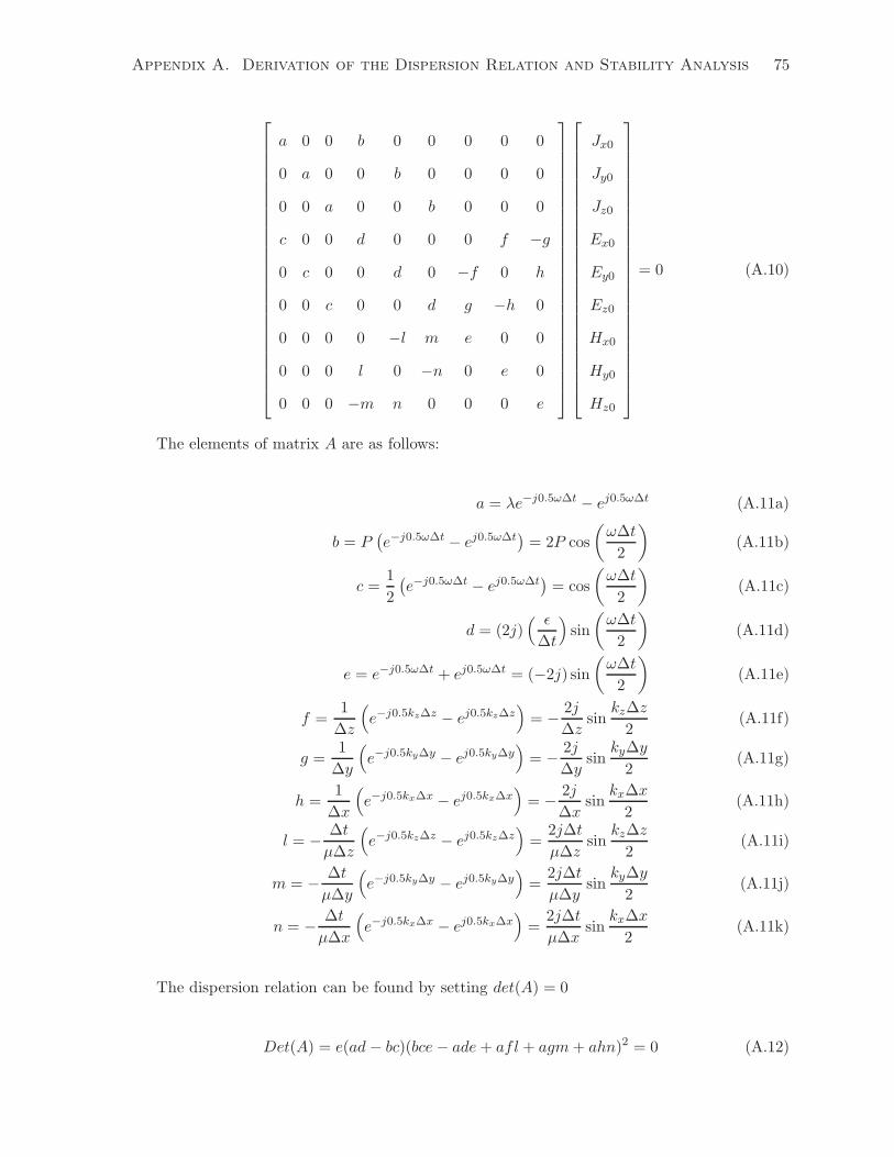
Appendix A. Derivation of the Dispersion Relation and Stability Analysis 75
a 0 0 b 0 0 0 0 0
0 a 0 0 b 0 0 0 0
0 0 a 0 0 b 0 0 0
c 0 0 d 0 0 0 f −g
0 c 0 0 d 0 −f 0 h
0 0 c 0 0 d g −h 0
0 0 0 0 −l m e 0 0
0 0 0 l 0 −n 0 e 0
0 0 0 −m n 0 0 0 e
Jx0
Jy0
Jz0
Ex0
Ey0
Ez0
Hx0
Hy0
Hz0
= 0 (A.10)
The elements of matrix A are as follows:
a = λe−j0.5ω∆t − ej0.5ω∆t (A.11a)
b = P(
e−j0.5ω∆t − ej0.5ω∆t)
= 2P cos
(
ω∆t
2
)
(A.11b)
c =1
2
(
e−j0.5ω∆t − ej0.5ω∆t)
= cos
(
ω∆t
2
)
(A.11c)
d = (2j)( ǫ
∆t
)
sin
(
ω∆t
2
)
(A.11d)
e = e−j0.5ω∆t + ej0.5ω∆t = (−2j) sin
(
ω∆t
2
)
(A.11e)
f =1
∆z
(
e−j0.5kz∆z − ej0.5kz∆z)
= − 2j
∆zsin
kz∆z
2(A.11f)
g =1
∆y
(
e−j0.5ky∆y − ej0.5ky∆y)
= − 2j
∆ysin
ky∆y
2(A.11g)
h =1
∆x
(
e−j0.5kx∆x − ej0.5kx∆x)
= − 2j
∆xsin
kx∆x
2(A.11h)
l = − ∆t
µ∆z
(
e−j0.5kz∆z − ej0.5kz∆z)
=2j∆t
µ∆zsin
kz∆z
2(A.11i)
m = − ∆t
µ∆y
(
e−j0.5ky∆y − ej0.5ky∆y)
=2j∆t
µ∆ysin
ky∆y
2(A.11j)
n = − ∆t
µ∆x
(
e−j0.5kx∆x − ej0.5kx∆x)
=2j∆t
µ∆xsin
kx∆x
2(A.11k)
The dispersion relation can be found by setting det(A) = 0
Det(A) = e(ad − bc)(bce − ade+ afl + agm+ ahn)2 = 0 (A.12)

Appendix A. Derivation of the Dispersion Relation and Stability Analysis 76
The simplified dispersion relation is:
bce = a(de − (fl+ gm+ hn)) (A.13)
equation (A.13) can be re-written as
a(de − (fl + gm+ hn))− bce = 0 (A.14)
Substitute in each of the variables, the dispersion relationship is:
(
λe−j0.5ω∆t − ej0.5ω∆t)
(
4 sin2(
ω∆t
2
)
−4∆t2
ǫµ∆x2sin2
(
kx∆x
2
)
− 4∆t2
ǫµ∆y2sin2
(
ky∆y
2
)
− 4∆t2
ǫµ∆z2sin2
(
kz∆z
2
))
+ (4j)P∆t
ǫcos2
(
ω∆t
2
)
sin
(
ω∆t
2
)
= 0
(A.15)
A.0.2 Detailed Stability Analysis
As mentioned in section 2.3, the dispersion relation in the r−plane is:
a3r3 + a2r
2 + a1r + a0 = 0 (A.16)
where
a3 = W +X + Y + Z = D(1− λ) (A.17a)
a2 = 3W +X − Y − 3Z = 4P +D(λ+ 1) (A.17b)
a1 = 3W −X − Y + 3Z = (D − 4)(λ− 1) (A.17c)
a0 = (4−D)(λ+ 1) (A.17d)
The stability condition is achieved when each element in the first column of the Routh table is
non-negative. A Routh table for equation (A.16) is constructed:
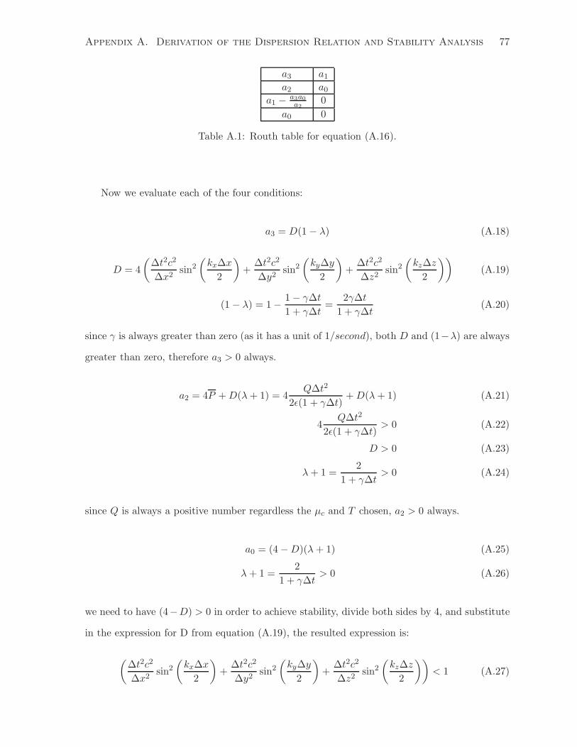
Appendix A. Derivation of the Dispersion Relation and Stability Analysis 77
a3 a1a2 a0
a1 − a3a0a2
0
a0 0
Table A.1: Routh table for equation (A.16).
Now we evaluate each of the four conditions:
a3 = D(1− λ) (A.18)
D = 4
(
∆t2c2
∆x2sin2
(
kx∆x
2
)
+∆t2c2
∆y2sin2
(
ky∆y
2
)
+∆t2c2
∆z2sin2
(
kz∆z
2
))
(A.19)
(1− λ) = 1− 1− γ∆t
1 + γ∆t=
2γ∆t
1 + γ∆t(A.20)
since γ is always greater than zero (as it has a unit of 1/second), both D and (1−λ) are always
greater than zero, therefore a3 > 0 always.
a2 = 4P +D(λ+ 1) = 4Q∆t2
2ǫ(1 + γ∆t)+D(λ+ 1) (A.21)
4Q∆t2
2ǫ(1 + γ∆t)> 0 (A.22)
D > 0 (A.23)
λ+ 1 =2
1 + γ∆t> 0 (A.24)
since Q is always a positive number regardless the µc and T chosen, a2 > 0 always.
a0 = (4−D)(λ+ 1) (A.25)
λ+ 1 =2
1 + γ∆t> 0 (A.26)
we need to have (4−D) > 0 in order to achieve stability, divide both sides by 4, and substitute
in the expression for D from equation (A.19), the resulted expression is:
(
∆t2c2
∆x2sin2
(
kx∆x
2
)
+∆t2c2
∆y2sin2
(
ky∆y
2
)
+∆t2c2
∆z2sin2
(
kz∆z
2
))
< 1 (A.27)
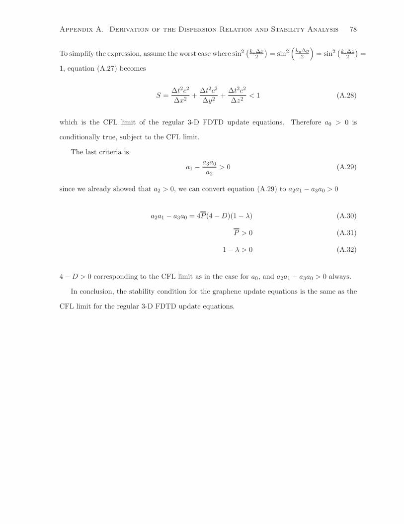
Appendix A. Derivation of the Dispersion Relation and Stability Analysis 78
To simplify the expression, assume the worst case where sin2(
kx∆x2
)
= sin2(
ky∆y2
)
= sin2(
kz∆z2
)
=
1, equation (A.27) becomes
S =∆t2c2
∆x2+
∆t2c2
∆y2+
∆t2c2
∆z2< 1 (A.28)
which is the CFL limit of the regular 3-D FDTD update equations. Therefore a0 > 0 is
conditionally true, subject to the CFL limit.
The last criteria is
a1 −a3a0a2
> 0 (A.29)
since we already showed that a2 > 0, we can convert equation (A.29) to a2a1 − a3a0 > 0
a2a1 − a3a0 = 4P (4−D)(1− λ) (A.30)
P > 0 (A.31)
1− λ > 0 (A.32)
4−D > 0 corresponding to the CFL limit as in the case for a0, and a2a1 − a3a0 > 0 always.
In conclusion, the stability condition for the graphene update equations is the same as the
CFL limit for the regular 3-D FDTD update equations.

References
[1] M. Dragoman, D. Neculoiu, D. Dragoman, G. Deligeorgis, G. Konstantinidis, A. Cis-
maru, F. Coccetti, and R. Plana, “Graphene for microwaves,” Microwave Magazine, IEEE,
vol. 11, no. 7, pp. 81 –86, Dec. 2010.
[2] J.-S. Moon and D. Gaskill, “Graphene: Its fundamentals to future applications,” Mi-
crowave Theory and Techniques, IEEE Transactions on, vol. 59, no. 10, pp. 2702 –2708,
Oct. 2011.
[3] Y.-M. Lin, C. Dimitrakopoulos, K. Jenkins, D. B. Farmer, H.-Y. Chiu, A. Grill, and
P. Avouris, “100-GHz transistors from wafer-scale epitaxial graphene,” Science, vol. 327,
no. 5966, p. 662, 2010.
[4] Y.-M. Lin and et al, “Wafer-scale graphene integrated circuit,” Science, vol. 332, no. 6035,
pp. 1294–1297, June 2011.
[5] A. Geim and K. Novoselov, “The rise of graphene,” Nature Materials, vol. 6, pp. 183–191,
Mar. 2007.
[6] A. Geim, “Graphene: Status and prospects,” Science, vol. 324, no. 5934, pp. 1530–1534,
Jun 2009.
[7] C. Lee, X. Wei, J. Kysar, and J. Hone, “Measurement of the elastic properties and intrinsic
strength of monolayer graphene.” Science, vol. 321, p. 385388, 2008.
[8] Y. Hernandez and et al, “High-yield production of graphene by liquid-phase exfoliation of
graphite,” Nature Nanotechnology, vol. 3, pp. 563 – 568, 2008.
79
REFERENCES 80
[9] D. Dikin and et al, “Preparation and characterization of graphene oxide paper,” Nature,
vol. 448, pp. 457–460, 2007.
[10] J. Meyer, A. Geim, M. Katsnelson, K. Novoselov, T. Booth, and S. Roth, “The structure
of suspended graphene sheets,” Nature, vol. 446, pp. 60–63, Mar. 2007.
[11] A. Reina, X. Jia, J. Ho, D. Nezich, H. Son, V. Bulovic, M. Dresselhaus, and J. Kong,
“Few-layer graphene films on arbitrary substrates by chemical vapor deposition,” Nano
Letters, vol. 9, no. 1, pp. 30–35, Jan. 2009.
[12] K. Kim and et al, “Large-scale pattern growth of graphene films for stretchable transparent
electrodes,” Nature, vol. 457, pp. 706–710, Feb. 2009.
[13] J. Haas, W. de Heer, and E. Conard, “The growth and the morphology of epitaxial mul-
tilayer graphene,” J. Phys. Matter, vol. 20, no. 32, p. 323202/127, Aug. 2008.
[14] V. C. Tung, M. Allen, Y. Yang, and R. Kaner, “High-throughput solution processing of
large-scale graphene,” Nat. Nanotechnol., vol. 4, no. 1, p. 2528, Jan. 2009.
[15] S. Bae and et al, “Roll-to-roll production of 30 inch graphene films for transparent elec-
trodes,” Nat. Natechnol., vol. 5, p. 574578, Jun. 2010.
[16] G. Deligeorgis, M. Dragoman, D. Neculoiu, D. Dragoman, G. Konstantinidis, A. Cismaru,
and R. Plana, “Microwave switching of graphene field effect transistor at and far from the
dirac point,” Applied Physics Letters, vol. 96, no. 10, pp. 103 105–3, Mar 2010.
[17] D. Neculoiu, G. Deligeorgis, M. Dragoman, D. Dragoman, G. Konstantinidis, A. Cisman,
and R. Plana, “Electromagnetic propagation in graphene in the mm-wave frequency range,”
in Microwave Integrated Circuits Conference (EuMIC), 2010 European, Sept. 2010, pp. 377
–380.
[18] G. Deligeorgis and et al, “Microwave propagation in graphene,” Appl. Phys. Lett., vol. 95,
no. 073107, 2009.

REFERENCES 81
[19] P. Russer, N. Fichtner, P. Lugli, W. Porod, J. Russer, and H. Yordanov, “Nanoelectronics-
based integrate antennas,” Microwave Magazine, IEEE, vol. 11, no. 7, pp. 58 –71, Dec.
2010.
[20] I. Llatser, C. Kremers, A. Cabellos-Aparicio, J. Jornet, E. Alarcon, and D. Chigrin, “Scat-
tering of terahertz radiation on a graphene-based nano-antenna,” in AIP Conference Pro-
ceedings, no. 1398, 2011, pp. 144 – 147.
[21] I. Llatser, C. Kremers, D. Chigrin, J. Jornet, M. Lemme, A. Cabellos-Aparicio, and E. Alar-
con, “Characterization of graphene-based nano-antennas in the terahertz band,” in Anten-
nas and Propagation (EUCAP), 2012 6th European Conference on, March 2012, pp. 194
–198.
[22] M. Dragoman, A. Muller, D. Dragoman, F. Coccetti, and R. Plana, “Terahertz antenna
based on graphene,” Journal of Applied Physics, vol. 107, no. 10, p. 104313, May 2010.
[23] A. Vakil and N. Engheta, “Transformation optics using graphene,” Science, vol. 332, pp.
1291–1294, Jun. 2011.
[24] L. Pierantoni, D. Mencarelli, and T. Rozzi, “Modeling of the electromagnetic/coherent
transport problem in nano-structured materials, devices and systems using combined TLM-
FDTD techniques,” in IEEE MTT-S Int. Microwave Symp. Dig., Jun. 2011.
[25] D. Mencarelli, L. Pierantoni, and T. Rozzi, “Graphene modeling by TLM approach,” in
Microwave Symposium Digest (MTT), 2012 IEEE MTT-S International, June 2012, pp. 1
–3.
[26] G. W. Hanson, “Dyadic greens functions and guided surface waves for a surface conduc-
tivity model of graphene,” Journal of Applied Physics, vol. 103, no. 064302, Mar. 2008.
[27] ——, “Quasi-transverse electromagnetic modes supported by a graphene parallel-plate
waveguide,” Journal of Applied Physics, vol. 104, no. 084314, 2008.
[28] G. Bouzianas, N. Kantartzis, C. Antonopoulos, and T. Tsiboukis, “Optimal modeling
REFERENCES 82
of infinite graphene sheets via a class of generalized FDTD schemes,” Magnetics, IEEE
Transactions on, vol. 48, no. 2, pp. 379 –382, Feb. 2012.
[29] V. Gusynin, S. Sharapov, and J. Carbotte, “Magneto-optical conductivity in graphene,”
Journal of Physics: Condensed Matter, vol. 19, no. 026222, 2007.
[30] K. Yee, “Numerical solution of initial boundary value problems involving maxwells equa-
tions in isotropic media,” IEEE Transactions on Antennas and Propagation, vol. 14, no. 3,
pp. 802–807, 1966.
[31] A. Pereda, L. Vielva, A. Vegas, and A. Prieto, “Analyzing the stability of the FDTD
technique by combining the von neumann method with the routh-hurwitz criterion,” Mi-
crowave Theory and Techniques, IEEE Transactions on, vol. 49, no. 2, pp. 377 –381, Feb
2001.
[32] A. Mock, “Pade approximant spectral fit for FDTD simulation of graphene in the near
infrared,” Optical Materials Express, vol. 2, no. 6, pp. 771 –781, 2012.
[33] J. G. Maloney and G. S. Smith, “The efficient modeling of thin material sheets in the finite-
difference time-domain (FDTD) method,” Antennas and Propagation, IEEE Transactions
on, vol. 40, no. 3, pp. 323–330, Mar. 1992.
[34] S. D. Gedney, “An anisotropic PML absorbing media for the FDTD simulatiohn of fields
in lossy and dispersive media,” Electromagnetics, vol. 16, no. 4, 1996.
[35] Y. Zhao, P. Belov, and Y. Hao, “Accurate modelling of left-handed metamaterials using
finite-difference time-domain method with spatial averaging at the boundaries,” J. Opt.
A: Pure Appl. Opt., vol. 9, pp. S468–S475, 2007.
[36] A. Taflove and S. Hagness, Computational Electrodynamics: The Finite-Difference Time-
Domain Method. Artech House, June 2000.
[37] C. C. Chao, S. H. Tu, H. I. Huang, C. C. Chen, and J. Y. . Chang, “Impedance-matching
surface plasmon absorber for FDTD simulations,” Plasmonics, vol. 5, pp. 51–55, 2010.

REFERENCES 83
[38] G. D. Bouzianas, N. V. Kantartzis, and T. D. Tsiboukis, “Consistent analysis and rigor-
ous characterization of infinite graphene layers via a subcell frequency-dependent FDTD
technique,” in General Assembly and Scientific Symposium, 2011 XXXth URSI, Aug. 2011.
[39] I. Llatser, C. Kremers, A. Cabellos-Aparicio, J. Jornet, E. Alarcon, and D. Chigrin,
“Graphene-based nano-patch antenna for terahertz radiation,” Photon Nanostruct: Fun-
damentals and Applications, vol. 10, no. 4, pp. 353–358, 2012.
[40] I. Llatser, C. Kremers, A. Cabellos-Aparicio, E. Alarcon, and D. Chigrin, “Comparison of
the resonant frequency in graphene and metallic nano-antennas,” in AIP Conf. Proc., no.
1475, Oct. 2012, pp. 143 –145.
[41] W. Thiel, “A surface impedance approach for modeling transmission line losses in FDTD,”
Microwave and Guided Wave Letters, IEEE, vol. 10, no. 3, pp. 89 –91, Mar 2000.
[42] J. Beggs, R. Luebbers, K. Yee, and K. Kunz, “Finite-difference time-domain implementa-
tion of surface impedance boundary conditions,” Antennas and Propagation, IEEE Trans-
actions on, vol. 40, no. 1, pp. 49 –56, Jan 1992.