fc-301d service manual - argent data
TRANSCRIPT

FC-301D SERVICE MANUAL
SHENZHEN FRIENDCOM TECHNOLOGY DEVELOPMENT CO.,LTD ADD: 2/F MULTIFUNCTION BUILDING DONGPENG INDUSTRIAL PARK WUHAO
ROAD NORTH SECTION OF HI-TECH PARK SHENZHEN 518057 CHINA TEL: +86-755-86026600 FAX: +86-755-86026300

- 1 -
TABLE OF CONTENTS
TABLE OF CONTENTS ........................................01..
SPECIFICATIONS ...........................................02
FC-301D CIRCUIT DIAGRAM.................................07
INTRODUCTION............................................08
FEATURES.................................................08
THEORY OF OPERATION....................................09
MAINTENANCE AND REPAIR................................18
PROGAMMING.............................................21
ALIGNMENT PROCEDURE...................................37
ALIGNMENT POINTS DIAGRAM..............................43
COMPONENT REPLACEMENT................................44
TROUBLESHOOTING GUIDE.................................48
WIRING DIAGRAM..........................................49
FC-301D DIGITAL BOARD PARTS LIST ........................50
DIGITAL BOARD SCHEMATIC ................................54
DIGITAL PCB ASSEMBLY ....................................58
FACTORY SETTING DIAGRAM ...............................60
EXPLODED VIEW & PARTS LIST .............................61

- 2 -
SPECIFICATION
GENERAL
Equipment Type…………………………………Data Radio
Performance Specification…………..................TIA/EIA-603 & ETS 300-113
Band …………………………………………...UHF/VHF
Channel Spacings………………………………25KHz,12.5KHz programmable
RF Output Power……………………………….1W / 5W Programmable
Modulation type ………………………………..16K0F3E,8K5F3E
Intermediate Frequency………………………… 45.1MHz & 455KHz
Number of Channels…………………………….16
Frequency Source ……………………………….Synthesizer
Operation Rating…………………………………Intermittent
5:5:90 ( TX: RX: Standby )
Power Supply ……………………………………12.5V DC Nominal Voltage
Temperature Range
Storage………………………………………from –40°C to +80°C
Operating……………………………………from –30°C to +60°C
Current Consumption
Standby (Muted) ……………………………≤40mA
Transmit 5 Watts RF Power …………………< 1.5A
Transmit 1 Watt RF Power…………………..<0.8A

- 3 -
Frequency Bands : ………………………………RX UHF: U1 400 – 470 MHz
…………………..…………….TX UHF: U1 400 – 470 MHz
Dimensions………………………………………..(120mm)L x (60mm)W x (20mm)H
Weight……………………………………………..≤150 grams
TRANSMITTER
Sustained Transmission…………………………… Nominal conditions
Time: 5 10 30 sec Power: >95% >95% >90%
Frequency Error…………………………………..±2.5 ppm
Frequency Deviation:
25kHz Channel Spacing……………………..≤±5.0kHz,
12.5kHz Channel Spacing……………………≤±2.5kHz,
Audio Frequency Response………………………. Within +1/-3dB of 6dB octave
@300Hz to 2.55kHz for 12.5kHz C.S @300Hz to 3.0khz for 25kHz C.S
Adjacent Channel Power
25kHz…………………………………………< 70 dBc @ Nominal Condition
<65 dBc @ Extreme Condition
12.5kHz ………………………………………< 60 dBc @ Nominal Condition
< 55 dBc @ Extreme Condition
Conducted Spurious Emission …………………….< -36 dBM
Modulation Sensitivity……………………………. 100mV RMS@60% peak Dev.
Hum & Noise:
25kHz Channel Spacing………………….….>40 dB (with no PSOPH)

- 4 -
12.5kHz Channel Spacing………………..……>36 dB (with POSPH)
Modulation Symmetry ……………………………..<10% Peak Dev@1kHz input
for nominal dev +20dB
Load Stability……………………………………No osc at >= 10:1 VSWR all
phase angles and suitable antenna No destroy at >= 20:1 all phase angle
RECEIVER
Sensitivity(12dB Sinad) …………………………..UHF <-117 dBm,
Amplitude Characteristic………………………….<±3dB
Adjacent Channel Selectivity:
25 kHz Channel Spacing …………………….≥70dB @ Nom.,
12.5kHz Channel Spacing…………………….≥60dB@Nom.,
Spurious Response Rejection………………………70dB
Image Response…………………………………… > 70 dB
IF Response ………………………………………. >70 dB
Others………………………………………………> 70 dB
Intermodulation Response Rejection………………≥65 dB
Conducted Spurious Emission @ Nominal Conditions………<-57 dBm
AF Distortion ………………………………………………....<5% @ Nom.,
<10%@ Extreme Condition
RX Hum & Noise:
25.0kHz CP……………………………………………< 40dB No PSOPH

- 5 -
12.5kHz CP ………………………………………..…< 40dB with PSOPH
Receiver Response Time …………………………….< 20ms
Squelch Opening sensitivity: ………………………-118dBm
Squelch Closing sensitivity ……………………….. -121dBm
Squelch Attack Time:
RF Level at Threshold ………………………… <40ms
RF Level at Threshold +20dB…………………<30ms
L.O. Frequency Temperature Stability…………….1 st <2.5 ppm,
2 nd <10 ppm for –30°C to +60°C
L.O. Frequency Aging Rate………………………….±2 ppm/year
REFERENCE CRYSTAL
Frequency…………………………………………………. 13MHz
Temperature Characteristic……………………………+/- 2.5PPM
from –30°C to +60°C
Aging Rate……………………………………………….< 2ppm/year in 1 st year <1ppm/year thereafter
TX to RX ………………………………………………… < 20
RX to TX ………………………………..……………….. < 25
ENVIRONMENTAL ( performance without degradation unless stated)
Temperature……………………………………………… deg C
Operating………………………………………………….-30° to +60°C Degradation
Specified@Extreme
Storage …………………………………………………… -40°C to +80°C

- 6 -
Recharging ……………………………………………… -10 to +55
ESD………………………………………………………. 20kV (C-MIC >= 15kV)
Vibration………………………………………………… MIL STD 810 C Procedures I,II,V
and IEC68 26
·Due to contintuning researching and development the company reserves the
right to alter these specifications without prior notice.

- 7 -
FC-301D CIRCUIT DIAGRAM

- 8 -
INTORDUCTION
The FC-301D Series of RF Link Modules from Friendcom utilizes the latest
technology in its design and manufacturing. Both the UHF and VHF models
are PLL (Phase Lock Loop Synthesizer) / microprocessor controlled, and offer
one to five watts of power with 16 channel capability. Multiple functions
including 1200 to 9600 baud rates,AC audio coupling,GMSK and FSK
modulation are standard in these fully programmable wide bandwidth RF Link
Module units.
FEATURES
● 16 Channels
●1 / 5 Watt Programmable Output
●12.5 / 25 kHz Programmable Channel Spacing

- 9 -
THEORY OF OPERATION
The Base Band signal circuits
It contains the CPU, power circuit ,TX signal circuit,RX signal circuit.
The CPU circuit and power circuit
From Block Digram above: The DC power was regulated to 8 volt by
IC500 ,and supplied to the RF part. IC504 convert 8 volt to 5volt and supply to
IC510. Q500 is RX power supply switch, Q502 is TX power supply switch.
IC501 supply 3.6V to PLL IC. Channels can be selected by the switch (CF3).
IC510 controls digital frequency synthesize by PLL STR ,PLL DATA and PLL
CCK.

- 10 -
The CPU SQ pin detect the signal from PIN14 of IC2. when there is no
receiveing signal, the input level is about 1.2V, and PIN8 of IC510 output high
level(5V). When detect input receiving signal, the input level is about 0V, and
PIN8 of IC510 output low level(5V).
TX signal circuit
From the above Block Diagram : IC801 is audio/Data and UART signal switch.
When the SW pin is high ,audio/data signal can go through IC801. S1 is a
switch between audio and data input, when transmit audio, MIC IN port is
shorted, when transmit data, DATA IN port is shorted. As it was data signal it
will pass through DATA-IN port and amplified by U1A, then it was coupling
by C431 and pass to U1B for amplify again;as it was audio signal it will pass

- 11 -
through MIC-IN port and amplified by U1B; then it will divide into two signal,
one will coupling by C405 R407 and fed to TCXO for TX modulation; the
other one was amplified by U1C,after coupling by C428,R404,C427 ;the voice
signal is filtered by U1D which is a low pass filter, the output of U1D is then
fed to VCO for TX modulation after coupling by C415,R403 again. Q401 is
a Wideband /narrow-band switch .
RX signal circuit
From the above Block Diagram; The resulting AF signal from IC2 enters base
band processing chip U2. First coupling by C412 and amplified by U2A ,then
it is filtered by U2B which is a low pass filter.After U2B,one signal pass
through IC801 and send to COM pin 2, one signal is amplify by audio
amplifierIC8, and sent to the horn directly. Q403 is a audio PA switch.

- 12 -
RF circuit
Main include PLL circuit / TX circuit /RX circuit
PLL Frequency Synthesizer
From the above Block Diagram : PLL circuit generates the first local oscillator
signal for reception and RF signal for transmission.
1. PLL Circuit
Step frequency of PLL can be 5.0 KHz or 6.25 KHz. A 13MHz reference
oscillator signal is divided at IC301 by a counter to generate a 5.0 KHz or 6.25
KHz reference frequency. Output signal from VCO is buffer amplified by
Q301 and divided at IC301 by a frequency divider. The divided signal is
compared with 5.0 KHz or 6.25 KHz reference signal in the phase
comparator of IC301. The output signal from phase comparator is filtered
through a low pass filter(Q320/Q321/ R39/C328/R318/R31/C327/R316/C326)

- 13 -
to generate a level D.C., and the level D.C. controls oscillator frequency by
controlling VCO.
2. VCO
The operating frequency is generated by Q302 in transmit mode and by Q307
in receive mode. Operating frequency generate a control voltage by phase
comparator to control varactor diodes so that the oscillator frequency is
consistent with the MCU preset frequency(D301、D302、D303 and D304 in
transmit mode, and D307、D308、D309 and D310 in receive mode). T/R pin is
set high level in receive mode, and low level in transmit mode. The output
from Q302 and Q307 is amplified by Q304 and sent to buffer amplifier.
3. Unlock Detector
An unlock condition appears if low level appears at MUXOUT pin of IC301.
Transmission is forbidden if this condition is detected by CPU IC510.

- 14 -
Receiver
The receiver utilizes double conversion superheterodyne (UHF)/(VHF).
1. Front-end RF Amplifier
The signal from antenna is amplified at LNA (Q15) after passing through a
transmit/receive circuit and a band pass filter
(D211/D212/D241/C264/C260/L25/L26). Before passing the first mixer
(T3、T4、TC3), the amplified signal is filtered through another band pass
filter(D208/D209/C240/C257/C258/L23/L24) to remove unwanted signals.

- 15 -
2. First Mixer
The signal from RF amplifier is mixed with the first local from PLL
frequency synthesizer circuit at the fix mixer (T3、T4、TC3) to create a
45.1MHz first IF signal. The first IF signal is then amplified by Q13 and fed
through a crystal filter (XF1) to further remove unwanted signals.
3. IF Amplifier
The first IF signal is amplified by Q13 before passing through crystal filter and
by Q12 after crystal filter and then enters IF processing chip IC2. The signal
from IC2 is mixed with the second oscillator signal again in IC2 to create a 455
KHz second IF signal. The second IF signal then passes through a 455KHz
ceramic filter (wideband: CF2,narrowband: CF1) to eliminate unwanted
signals before it is amplified and detected in IC2.
4. Narrowband/Wideband Switch Circuit
Pin W/NCON of IC510 outputs narrowband (high level) and wideband (low
level) controlling signal respectively to turn on corresponding diode-connector,
and to choose ceramic filter CF2 (wideband) or CF1 (narrowband) to filter
useless spurious signal.

- 16 -
Transmitter
1. RF Power Amplifier
The transmit signal from VCO buffer amplifier (Q304、Q111) is amplified by
Q1 and Q2. The amplified signal is then amplified by the power amplifier I102
to create 5.0W RF power.
2. Antenna Switch and LPF
Output signal from RF amplifier passes through a low-pass filter network and
a transmit/receive switch circuit comprised of D102,D106 and D107 before it
reaches the antenna terminal. D106 and D107 is turned on (conductive) in
transmit mode and off (isolated) in receive mode.
- 17 -
3. APC
The automatic power control (APC) circuit stabilizes the transmit output
power by detecting the forward and backward power of final stage amplifier.
IC1 (2/2) compares the preset reference voltage with the voltage obtained from
the regulated power signal. APC voltage is proportional to the forward and
backward power. The output voltage controls the bias voltage of power
amplifier module.The output power can be controlled by the software.

- 18 -
MAINTENANCE AND REPAIR
GERNERAL
When removing or fitting, use the Exploded View and Parts List, located on
page 61 in conjunction with the following procedures:
·WARNING: Disconnect the FC-301D from all external equipment at the
connector prior to disassembly.
REMOVING & REPLACING THE UPPER COVER
Removing the Upper Cover:
1. Unscrew the four side cover
mounting screws located on the side
cover of the radio.
To replace the Upper Cover: 1. Reverse the steps taken to remove the
Upper Cover.
Figure 1-Upper cover removal

- 19 -
REMOVING&REPLACING THE INTERPHASE CONNECTION BOARD
Removing the interphase connection board:
1.Remove the Upper Cover (refer to Removing & Replacing the Upper
Cover).
2.Disconnect the DB9 pin connector on CON401.
3.Unscrew the two mounting screws on the Amplifier module.
4.Remove the interphase connection board directly.
To replace interphase connection board:
1. Reverse the steps taken to remove the interphase connection board
Figure 2 Interphase connection board removal

- 20 -
REMOVING & REPLACING THE RF BOARD
Removing the RF Board Assembly:
1.Remove the Upper Cover (refer to Removing & Replacing the Upper
Cover).
2.Remove the interphase connection board (refer to Removing & Replacing
the interphase connection board).
3. Unscrew the 4 mounting screws
4. Unsolder the antenna connector cable.
5. Remove the RF Board Assembly.
To replace the RF Board Assembly: 1.Reverse the steps taken to remove the RF Board Assembly.
Figure 3 RF BOARD Removal

- 21 -
PROGRAMMING
The detailed information on programming the FC-301D radio in following
procedures.
Ⅰ. To start the FC-301/D Program Software and read the parameters of
FC-301/D RF Link Module
Firstly make sure to connect data port J1 of FC-301D with PC via
RS232 data cable.
Double click the "FC301D.exe". The software will enter into main
interface of FC-301D as the following:

- 22 -
Run the ‘Port’ in the main menu or press the Icon ‘Port ’ , The
software will enter into the Port parameter setting interface.

- 23 -
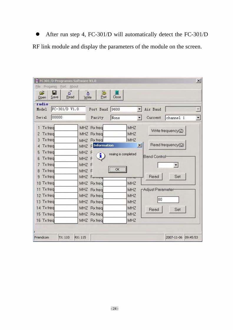
Run ‘ Program ’ -> ‘ Read ’ in the main menu, The software will
detect and read the parameters of FC-301D.
- 24 -
After run step 4, FC-301/D will automatically detect the FC-301/D
RF link module and display the parameters of the module on the screen.

- 25 -
Ⅱ. To change the parameters of the RF link module
After reading the previous parameters, User can change the parameters of
the module to new ones.
Model:Only for check, it can not be changed.
Serial No:Input 5 digits for ID code. Zero will be added to the front.
The value less than 65536.
Port Baud:Optional from the list box
Parity: Optional from the list box
Channel: Only for check, it can not be changed

- 26 -
Ⅲ. To write the parameters into the module
Run ‘Program’ -> ‘ Write ’ in the main menu, The changed parameters
will be written into the FC-301/D module.

- 27 -
Ⅳ. To read / write the frequency
Click the button ‘Read Frequency’, the frequency of the channel from
1-16 will be displayed on the screen.

- 28 -

- 29 -
New frequency can be input into each channel and click the ‘Write
Frequency’ button, the new frequency will be written into the module.

- 30 -

- 31 -
Ⅴ. The switch between 12.5kHz and 25kHz channel spacing
In the ‘Band Control ’ interface, Click ‘Read’ , the current channel
spacing 12.5kHz or 25kHz can be read out. Click ‘Set’, the selected
channel spacing 12.5kHz or 25kHz can be written into the module.

- 32 -
Ⅵ. To adjust the parameters
While the module works in transmission or reception status on one
fixed frequency, Click ‘Set’ in ‘Adjust Parameter’ to adjust the sensitivity
or the RF power on one frequency. Click ‘Read’ to read the adjusted
parameters of the current frequency.
Turning Value ,the value range is between 0 and 255; when its value is
0 ,the corresponding voltage of CPU APC/TV pin is 4.0V,as the value
increase the voltage of CPU APC/TV will decrease correspondingly . when
its value is 255, the Voltage of CPU APC/TV pin is 0V. it is in inverse
proportion relationship between two value.
Set turning value of RX (TV Value)
Fristly adjust CON1 pin8 SW port to low level and change RF at the
status of RX ;

- 33 -
S
econdly input the corresponding value in ‘Adjust Parameter’ according to
channel frequency ;you will see ‘Setting successful’after you click ‘set’.
Otherwise you will see ‘Setting no answer’which indicate setting fail.
Thirdly,after setting success you can wait for 10 seconds or switch
channel button to make the newest parameter be stored in CPU.

- 34 -
Read the Turning Value of RX (TV Value)
Fristly adjust CON1 pin8 SW port to low level and change RF at the
status of RX ;
Secondly click the button ‘Read’ in Adjust Parameter,you will see
‘Reading success’message and the detail parameter below; otherwise you
will see ‘Reading no answer’and it indicate read failed it need to read
again .(Without necessary please remmeber not to change the turning
value which have set in factory ,otherwise it will affect other
technologic parameter in RF)
Set turning value of TX (APC Value)
Fristly adjust CON1 pin8 SW port to low level and change RF at the
status of RX ;
Secondly input the corresponding value in ‘Adjust Parameter’ according
to channel output frequency ;you will see ‘Setting successful’after you
click ‘set’.Otherwise you will see ‘Setting no answer’which indicate
setting fail.
Thirdly,after setting success you can switch channel button to make the
newest parameter be stored in CPU.
Read the Turning Value of TX (TV Value)
Fristly adjust CON1 pin8 SW port to low level and change RF at the
status of TX ;
Secondly click the button ‘Read’ in Adjust Parameter,you will see

- 35 -
‘Reading success’message and the detail parameter below; otherwise you
will see ‘Reading no answer’and it indicate read failed and need to read
again .
Ⅶ. To save or open parameter file
Run ‘File’->‘Save’ menu, The ‘Save’ interface will be displayed on the
screen, Input the file name for saving, and press ‘Save’ button, the current
parameters of the module will be saved into the appointed file for later use.

- 36 -
Run ‘File’->‘Open’ menu, The ‘open’ interface will be displayed on the
screen, Choose the file name which saved the parameters, and press ‘Open’
button, the parameters of the module saved in the file will be displayed on
the screen.

- 37 -
ALIGNMENT PROCEDURE
The FC-301D is by design, broad band covering UHF(400-470 MHz) and
should require no special alignment, unless repairs are performed on the
receiver portion. Should repairs be necessary, use the "Alignment Points
Diagram" on page, in conjunction with the following procedures:
PCB Testing
1.Adjust the power supply voltage to 12.5V before connect FC-301D to
power supply, switch the power on. Then set up the channal frequency (Refer
to the attached list on page 60 )
2. Switch CF3 to 16 channels and set the transceiver to TX . Adjust VR1 and
read the TX frequency from the equipment until the TX frequency is
469.9750MHz .adjust TC301 and test the VT voltage of TP1 until the voltage
is 4.7±0.2V; switch CF3 to 8 channels and test the VT voltage ,it should be
0.7±0.2V
3. Switch CF3 to 16 channels and set the transceiver to RX . Read the TX
frequency from the equipment ,it should be 424.8750MHz .adjust TC302 and
test the VT voltage of TP1,the voltage should be 4.7±0.2V; switch CF3 to 8
channels and test the VT voltage ,it should be 0.7±0.2V
Audio Test of TX

- 38 -
1.Set Wireless Conmmunication Test set at the status of RX Test
2. Set the audio out of Wireless Conmmunication Test set as 1K; the amplitude
of sinusoidal signal as 100mV.
3.Connect the audio output to CONI pin1 of FC301D,switch S1 to
MIC-IN;then adjust the RF at the status of TX , connect the audio output to
TP4 ,adjust VR403 for a reading of audio signal amplitude as 58mV and
distortion is less than 3%
4.Connect the audio output to CONI pin1 of FC301D,switch S1 to
DATA-IN;then adjust the RF at the status of TX , fristly connect the audio
output to TP3 ,adjust VR404 for a reading of audio signal amplitude as
100mV and distortion is less than 3%; Secondly connect the audio output to
TP4 ,adjust VR403 for a reading of audio signal amplitude as 59mV and
distortion is less than 3%; thirdly connect the audio output to TP5 ,adjust
VR407 for a reading of audio signal amplitude as 0.7V and distortion is less
than 3%.
RF Test of TX
1.Set Wireless Conmmunication Test Set at the status of TX Test.
2.Fristly testing TP6 , fine turning VR1 to control the error between TX
frequency and standard frequency among ±300Hz.
3.Set the channel space as wide-band,fristly test TP6 by set the output

- 39 -
frequency of Wireless Conmmunication Test set as 1KHz; the amplitude of
sinusoidal signal as 100mV.Secondly test channe 1 ,8 and 16 separately for a
reading of TX power 20mV+5mW, frequency deviation 3KHZ+0.5KHz and
distortion is less than 3%; Also off the output signal of Test Set the frequency
deviation should less than 70Hz.
4.Set the channel space as narrow-band,fristly test TP6 by set the output
frequency of Wireless Conmmunication Test set as 1KHz; the amplitude of
sinusoidal signal as 100mV.Secondly test channe 1 to chennel 8 separately for
a reading of TX power 20mV+5mW, frequency deviation 1.5KHz+0.5KHz
and distortion is less than 3%; Also off the output signal of Test Set the
frequency deviation should less than 70Hz.
Passband Test of RX
1. Setting of Test Set(HP8920) as follow :
TX Test---- SPEC ANL---- RF Ant-----Center Freq -------Input scanning
frequency------Ref Level set as - 20dBm-------Span set as
200MHz-------Main select RF Gen -------Eixed---------Amplitude set as -
40dBm---- RF Out.
2. Connect the ANT IN port of Test Set to TP7 , and see its frequency spectrum
as below
3. Each frequency have to set to corresponding turning value ,for detail turning
value please refer to attached diagram on page ? ? ? ?

- 40 -
TX Test of FC301D
1.Set Wireless Conmmunication Test Set at the status of TX Test; Also set
FC301D at the status of TX .
2.Fine turning VR1 to meet the error between TX frequency and standard
frequency among ±300Hz.
3.Please refer to the diagram on page ? to adjust turning value for each
channel , to control the TX output power of each channel to be 4.5W-6W and
current to be less than 1.5A
4.Set the output frequency of Wireless Conmmunication Test set as 1KHz; the
amplitude of sinusoidal signal as 100mV;testing for reading of frequency
deviation to be 3KHz+0.5KHz for wide-band and 1.5KHz+0.5KHz for
narrow band; and the distortion is less than 3%; Also off the output signal of
Test Set the frequency deviation should less than 80Hz.
RX Wide Band Test of FC-301D
1.Set Wireless Conmmunication Test Set at the status of TX Test , and the

- 41 -
modulation signal of Test set have to be setted field intensity as
1mv ,frequency as 1KHz and frequency deviation as 3kHz. Also set FC301D
at the status of RX
2.Please refer to wiring diagram and operation on page 49 to testing for a
reading of AF OUT level to be 210+20mV and ditortion less than 5%
3.Please refer to Turning Value on page ? ,set the RF output signal of the Test
Set to 0.28μV and test the Sinad,it should be better than 12dB.
4.When Sinad drop to be 10dB, SQ should be high level output and Voltage
range should be more than 4.5V; When Sinad rise to more than 12dB, SQ
should be low level output and Voltage range should be less than 0.4V;
5.Testing the RSSI output level should to be 2.2V-0.8V
6.Testing the audio output power to 2.2V+50mV.
RX Narrow Band Test of FC301D
1.Set Wireless Conmmunication Test Set at the status of TX Test , and the
modulation signal of Test set have to be setted as follow ;field intensity as
1mv ,frequency as 1KHz and frequency deviation as 1.5kHz. Also set
FC301D at the status of RX
2.Please refer to wiring diagram and operation on page ? to testing for a
reading of AF OUT level to be 210+20mV and ditortion less than 5%
3.Please refer to Turning Value on page 60,set the RF output signal of the Test
Set to 0.35μV and test the Sinad,it should be better than 12dB.

- 42 -
4.When Sinad drop to be 10dB, SQ should be high level output and Voltage
range should be more than 4.5V; When Sinad rise to more than 12dB, SQ
should be low level output and Voltage range should be less than 0.4V;
5.Testing the RSSI output level should to be 2.2V-0.8V
6. Testing the audio output power to 2.2V+50mV.

- 43 -
ALIGNMENT POINTS DIAGRAM
DIGITAL BOARD ALIGNMENT POINTS
CHANNEL SELECT SWITCH

- 44 -
COMPONENT REPLACEMENT
Surface Mount Components
Surface mount components should always be replaced using a temperature
controlled soldering system. The soldering tools may be either a temperature
controlled soldering iron or a temperature controlled hot-air soldering station.
A hot-air system is recommended for the removal of components on these
boards. With either soldering system, a temperature of 700° F (371° C) should
be maintained.
The following procedures outline the removal and replacement of surface
mount components. If a hot-air soldering system is employed, see the
manufacturer’s operating instructions for detailed information on the use of
your system.
CAUTION: Avoid applying heat to the body of any surface mount
component using standard soldering methods. Heat should be applied
only to the metalized terminals of the components. Hot-air systems do
not damage the components since the heat is quickly and evenly
distributed to the external surface of the component
CAUTION: The CMOS Integrated Circuit devices used in this
equipment can be destroyed by static discharges. Before handling one
of these devices, service technicians should discharge themselves by
touching the case of a bench test instrument that has a 3-prong power

- 45 -
cord connected to an outlet with a known good earth ground. When
soldering or desoldering a CMOS device, the soldering equipment
should have a known good earth ground.
Surface Mount Removal 1.Grip the component with tweezers or small needle nose pliers.
2.Alternately heat the metalized terminal ends of the surface mount component
with the soldering iron. If a hot-air system is used, direct the heat to the
terminals of the component. Use extreme care with the soldering equipment
to prevent damage to the printed circuit board (PCB) and the surrounding
components.
3.When the solder on all terminals is liquefied, gently remove the component.
Excessive force may cause the PCB pads to separate from the board if all
solder is not completely liquefied.
4.It may be necessary to remove excess solder using a vacuum de-soldering
tool or Solder wick. Again, use great care when de-soldering or soldering on
the printed circuit boards. It may also be necessary to remove the epoxy
adhesive that was under the surface mount component and any flux on the
printed circuit board.
Surface Mount Component Replacement 1. “Tin” one terminal end of the new component and the corresponding pad of
the PCB. Use as little solder as possible.

- 46 -
2.Place the component on the PCB pads, observing proper polarity for
capacitors, diodes, transistors, etc.
3.Simultaneously touch the “tinned” terminal end and the “tinned” pad with
the soldering iron. Slightly press the component down on the board as the
solder liquefies. Solder all terminals, allowing the component time to cool
between each application of heat. Do not apply heat for an excessive length of
time and do not use excessive solder.
With a hot-air system, apply hot air until all “tinned” areas are melted and the
component is seated in place. It may be necessary to slightly press the
component down on the board. Touch up the soldered connections with a
standard soldering iron if needed. Do not use excessive solder.
CAUTION: Some chemicals may damage the internal and external
plastic parts of the radio.
4.Allow the component and the board to cool and then remove all flux from the
area using alcohol or another approved flux remover.
Surface Mounted Integrated Circuit Replacement
Soldering and de-soldering techniques of the surface mounted IC’s are similar
to the above outlined procedures for the surface mounted chip components.
Use extreme care and observe static precautions when removing or replacing
the defective (or suspect) IC’s. This will prevent any damage to the printed
circuit board or the surrounding circuitry.

- 47 -
The hot-air soldering system is the best method of replacing surface mount
ICís. The IC’s can easily be removed and installed using the hot-air system.
See the manufacturerís instructions for complete details on tip selection and
other operating instructions unique to your system. If a hot-air system is not
available, the service technician may wish to clip the pins near the body of the
defective IC and remove it. The pins can then be removed from the PCB with a
standard soldering iron and tweezers, and the new IC installed following the
Surface Mount Component Replacement procedures. It may not be necessary
to “tin” all (or any) of the IC pins before the installation process.

- 48 -
TROUBLESHOOTING GUIDE
SYMPTOM S
CAUSES
COUNTERMEASURES
Unit does not work
1.No power incomplete connection
2. No input voltage of 5V or 8V 3. CPU does not work 4. EEPROM fail 5. Channel error 6. PLL error
1.Check COM1 connection 2. Check IC500、IC504 3. Check IC510 4. Check IC502 5. Check CF3 6. Check TCXO、VCO、PLL IC
Bad RX Sensitivity
1.Antenna signal short-circuit 2.Antenna signal open-circuit 3. Bad electronic turner 4. Defective high frequency
amplifier 5. Bad mixer 6. Local signal amplitude
become small 7. Bad 1st and 2nd intermediate
frequency
1. Check D106 D107 2. Antenna loose weld 3. Check L23 L24 L25 L26 4. Replace Q15 5. Check IC3 T3 T4 6. Check D103 Q111 7. Check XF1 XF2 IC2
Defective RX
1. No output signal 2. Bad signal waveform 3. Bad stability of VCO
1. Replace IC801 2. Check U2 c412 c404 3. Check component of VCO
PLL Error
1. TCXO frenquency error 2. Bad stability of VCO 3. PLL can’t be locked
1.Check crystal oscillator of TCXO 2.Check the component of
TX/RXVCO 3. IC301 Q321 Q320 C327
Low TX Power
1. Bad amplfier circuit 2. Bad APC circuit
1. Replace IC102 2. Check D102 IC1
No TX Power
1. No power on TX 2. No signal on driver 3. Bad amplfier circuit 4. Bad APC circuit
1. Check Q502 Q503 2. Check Q1 Q2 D101 3. Check IC102 D102 4. Check IC1
No Modulation
1. No input signal 2. No TX signal
1. Check IC801 2. Check U1 R403 R404
- 49 -
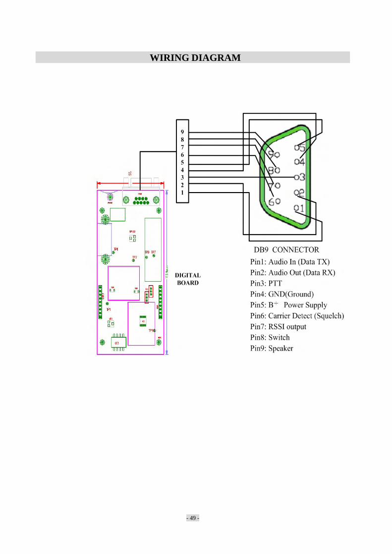
WIRING DIAGRAM

- 50 -
FC-301D DIGITAL BOARD PARTS LIST

- 51 -

- 52 -

- 53 -

- 54 -

- 55 -

- 56 -

- 57 -

- 58 -

- 59 -

- 60 -
FACTORY SETTING DIAGRAM
Channel
RX Frequency
RX Turning Value (TV)
TX
Frequency TX Turning Value (APC)
1
400.1250MHZ
170
400.1250MHZ
65
2
405.1250MHZ
165
405.1250MHZ
65
3
410.1250MHZ
160
410.1250MHZ
65
4
415.1250MHZ
155
415.1250MHZ
65
5
420.1250MHZ
150
420.1250MHZ
65
6
425.1250MHZ
145
425.1250MHZ
65
7
430.1250MHZ
140
430.1250MHZ
65
8
435.1250MHZ
135
435.1250MHZ
65
9
436.1250MHZ
130
436.1250MHZ
65
10
440.1250MHZ
130
440.1250MHZ
65
11
445.1250MHZ
125
445.1250MHZ
65
12
450.125MHZ
120
450.1250MHZ
65
13
455.1250MHZ
115
455.1250MHZ
65
14
460.1250MHZ
110
460.1250MHZ
65
15
465.1250MHZ
105
465.1250MHZ
65
16
469.9750MHZ
100
469.9750MHZ
65
From above diagram ,TX Turning Value is base on 5W normal output
power,please refer to The Manual of FC-301/D Program Software if you need
other Turning value base on other output power.

- 61 -
EXPLODED VIEW & PARTS LIST
ITEM # NAME QUANTITY DESCRIPTION
1 Label 1 self-adhesive paper
2 Front crust 1 stainless steel
3 Interphase connection board 1 Standard component
4 Plug-In unit 1 Standard component
5 PCB board 1 Standard component
6 Shielding case 1 Tinplate (nickel plating)
7 Shielding case B 1 Tinplate (nickel plating)
8 Shielding case C 1 Tinplate(nickel plating)
9 Cold sink 1 aluminum sheet
10 Back crust 1 Standard component
11 Screw 4 Standard component
12 Screw for DB9 2 stainless steel
13 Cooper pillar 6 stainless steel
14 Antenna connector 1 Standard component
15 Antenna spacer 1 Standard component
16 DB9 connector 1 Standard component
17 Shielding case D 1 Tinplate (nickel plating)
18 Cold silica gel 2 silica gel
19 IC module 1 Standard component

- 62 -