fast one-time programming (otp) and a … papers/midem_44(2014)2p104.pdf · programming...
TRANSCRIPT

104
Original scientific paper
MIDEM Society
Fast One-Time Programming (OTP) and a Programming Verification Solution using Zener Diodes in a Standard CMOS ProcessJanez Trontelj
Faculty of Electrical Engineering, Ljubljana, Slovenia
Abstract: This article describes an effective, low-cost solution for sequential, one-time programming (OTP) and verification of zener diodes in an electronic micro-system. Using the proper structures of zener diodes (also known as ‘zener zap’) in a standard CMOS process, it is possible to achieve better accuracy in high-precision integrated circuits. For this purpose a solution has been developed for fast programming and programming verification of several zener zap structures on the ASIC (Application Specific Integrated Circuit). The entire zapping process for 250 zener zap structures is completed in the range of a few tens of milliseconds. This solution has been implemented for wafer sorting, and as well for packaged integrated circuits. It was successfully verified in the industrial production of more than ten million- high precision, electronic micro-systems with a remarkable overall yield of 97%.
Keywords: OTP, Zener zap, ASIC, DAQ, burn pulse, antifuse
Hitra metoda za enkratno programiranje in preverjanje pravilnosti programiranja s pomočjo zener diod v standardnem CMOS procesuIzvleček: Članek opisuje učinkovit, nizko cenovni pristop za zaporedno, enkratno programiranje kakor tudi preverjanje pravilnega programiranja zener diod v elektronskem mikrosistemu. Z uporabo posebnih struktur integriranih zener diod (zener zap – zener antivarovalke) je v standardnem CMOS procesu mogoče doseči večjo natančnost integriranih vezij. V ta namen je bila razvita metoda za hitro, zaporedno programiranje več zener antivarovalk. Celoten postopek programiranja in verifikacije za 250 zener struktur je končan v času nekaj deset milisekund. Rešitev je bila uporabljena za meritve elektronskih mikrosistemov na silicijevih rezinah in tudi na posameznih čipih v ohišjih. Uspešno smo jo preverili v industrijski proizvodnji več kot deset milijonov visoko občutljivih integriranih vezij s celokupnim izplenom 97%.
Ključne besede: Enkratno programiranje, Zener varovalka, Vezja po naročilu, Zajem podatkov, pulz za prežig, antivarovalka
* Corresponding Author’s e-mail: [email protected]
Journal of Microelectronics, Electronic Components and MaterialsVol. 44, No. 2 (2014), 104 – 108
1 Introduction
In modern industry there is a huge demand for high-precision, low-cost, fully integrated analog sensors. Over the years, several methods have been implement-ed to overcome the tolerances of the integrated circuit fabrication process. Although ratiometric design prin-ciples may be successfully adopted, there is still a need for finer methods to adjust critical parameters of the in-tegrated sensors. Here various, one-time programming methods (OTP) take place - such as laser trimming, poly fuse burning and zener-zapping. By using these methods, we can significantly improve the production
yield and fulfill the requirements for accuracy of high-precision integrated circuits. This is usually done on the wafer level at wafer sort, but sometimes it must be also implemented for packaged parts - to eliminate the so-called ‘package effect’. It is evident that during dic-ing and packaging there may be a certain amount of stress applied to the sensitive sensor structures. So the overall accuracy of the sensor can be easily affected. This problem can be resolved even after packaging - by using automated measurements, handling, and fine-trimming of the packaged microelectronics systems.

105
J Trontelj; Informacije Midem, Vol. 44, No. 2 (2014), 104 – 108
This article describes a one-time programming tech-nique that uses zener-zapping. This well- established method creates antifuse devices. The term ‘antifuse’ describes an element which initially represents an open circuit, but can be later irreversibly changed to approach a short circuit. Such an element can be im-plemented with a reverse biased zener diode. This is a small, subsurface lateral N+, P+ structure. When the ze-ner diode programming current is increased, a tempo-rary avalanche breakdown in a P-N junction is forced. This causes localized heating and subsequent migra-tion of metallization across the junction (spiking). In other words, zener zapping is a short current pulse to the reverse biased zener diode. The resistance of the zapped diode is drastically changed after the OTP. This very interesting process is described in more detail in [1] and [2].
This article is not intended to describe zener zapping structures in detail. Such cells are now available as standard parts in design libraries for several technolo-gies. Additional improvements of various OTP methods are constantly evolving. Examples for this are described in [3], [4] and [5]. The trend is in further increasing the reliability, while reducing the zapping current.
Unfortunately, very little information is available on im-plementing the zapping procedure. When we began to deal with this topic, we experienced quite a few diffi-culties in achieving a fast and consistent zener zapping. We noticed that other teams also had a lot of trouble with this, and that our assistance was welcome. So, the main focus of this article is to describe how to create low-cost, fast as possible and reliable communication hardware to implement a test, a statistical analysis, and an OTP solution. Moreover, all this was developed to test our, in the LMFE (Laboratory for Microelectronics from Faculty of Electrical Engineering) designed ASIC with a high-precision magnetic sensor. In this case, a widely available and proven OTP zener zap cells from the silicon foundry technology library were used.
Figure 1 presents an actual photograph of a small part of the zener zap array on our ASIC. A photograph of four zener zap structures was taken at 3000x magnifi-cation. To take this photo, some layers above the zener zap structures had to be removed. Unfortunately, the entire zener zap structure is not at the same level, so some parts of the photograph are a little bit out of fo-cus.
The zener zapping method has numerous benefits. A zener diode is commonly available in all standard CMOS processes, and therefore represents no significant extra cost in fabrication. Each diode can be controlled by a single selection transistor. So, it is relatively easy to im-
plement a mixed mode sequential system for selecting and programming each zener diode separately. This approach usually requires one additional pin on the circuit. Also quite important is the fact that no life-time reliability problems of properly trimmed zener zaps are expected. The reason for this is that during OTP, no damage is caused to the other layers or the passivation on the silicon wafer surface. So, all affected structures remain safely isolated from the harsh environmental in-fluences, before device packaging takes place.
Figure 1: Zener zap structure photograph taken at 3000x magnification.
However, besides occupying some extra silicon, there are two major problem areas identified. One is in sup-plying the correct amount of current for effective burn-ing, and the second one is about defining the optimal burn pulse duration and shape. The final resistance of the zapped diode is additionally depending on the amount of the supplied current after the initial modi-fication of the P-N junction is done [2]. Last but not at least, for industrial production it is also quite essential to obtain as brief as possible programming and pro-gramming verification time.
In our case only one pin of the ASIC is reserved for OTP communication implementation. As the basis for the project, we decided to use a low-cost USB (or alter-natively ‘PC Card’) data acquisition card (DAQ) [6] and some extra, in-house designed hardware. For improved reliability, a sort of adaptive OTP pulse was developed. It can be automatically readjusted for each wafer lot, or even during testing each wafer separately. The de-scribed solution was practically verified in burning sev-eral millions of zener zap devices. It is capable to do the OTP of 250 zener zaps on one ASIC in approximately a 4 millisecond time frame. Besides for communication purposes, the DAQ card may also be used for taking various measurements, and according to measurement results, actual trimming of the measured sensor on the ASIC can be performed.

106
2 OTP procedure description
In this section the OTP method is described that was proposed for our high-precision magnetic sensor ASIC. In this case, besides the required selective trimming of critical parameters, unique identification of each mi-croelectronic system was also required. So each micro system is given a unique serial number. This enables us to easily compare the measured parameters on wa-fer sort with later measured parameters on packaged parts. In our particular example, 250 zener zap struc-tures for various OTP features are necessary. As we determined before, one pin of the ASIC is enough to implement the suggested OTP procedure. Basically, what we need is some sort of a pulse train, to access each zener element in a zener zap array. The train of pulses contains by default the information about the communication clock. When adopting different pulse levels, it can carry additional information. Figure 2 pre-sents the proposed pulse train with different levels and their meaning.
Figure 2: Pulse train with described meaning of differ-ent levels.
To prevent undesired false zapping during electrostatic discharge on the programming pin, there is a unique sequence of pulses in the beginning of the pulse train. This unlocks further recognition of the pulse train and enables eventual zener zapping. Figure 2 shows four different levels of pulses. The lowest level is the micro system reset. A normal level represents a clock with no programming action. This level only addresses the next zener diode. A higher level represents temporar-ily programming in shadow RAM (for a preview of the eventual OTP) on the currently selected zener zap. This state is active, until reset or the micro system power down takes place. This enables us to do evaluation and verification of the ASIC behavior before the final OTP is done. Furthermore, the highest level of the pulse repre-sents an action of irreversible OTP, or with other words – zener zapping.
After the zener zapping is completed, it is possible to send another pulse train to the programming pin, now without using the zener zapping highest pulse level. By temporarily setting up and using one, additional output pin on the ASIC, resistance of each zapped and un-zapped antifuse can be measured and verified. This further enhances the reliability and control of the zener zapping process.
3 Implemented methodology
The standard method for zener zapping is to discharge a small capacitor over a reverse biased zener diode. This forces a quite well-defined and repeatable avalanche breakdown in a P-N junction. When properly selected, the desired pulse width from 1 µs to 3 µs [2] can be eas-ily achieved. The problem is that this method needs additional time to sufficiently recharge the capacitor. A drawback is also evident, that during programming the charging current must be disconnected from the capacitor. This additionally slows down the effective-ness of this method.
Another approach is to use expensive dedicated equip-ment that is capable to drive and precisely control the current and shape for a relatively short burn pulse. We had a chance to compare the results from our low-cost solution with a similar solution on such relatively ex-pensive equipment (approx. cost ratio 1:50), and our solution was superior.
Figure 3: Simplified schematic for generation of vari-able OTP pulse.
Figure 3 describes the method proposed in this article. An adjustable voltage regulator is controlled by the analog output DAQ1 pin of the DAQ card to achieve different levels of the pulse train. The burn pulse is triggered by the DAQ2 digital signal and a simple de-lay circuit with a Schmitt trigger, and then added to the pulse train via small capacitor. Trimmers are used for fine adjusting the amplitude and pulse width. To achieve approx. 1 μs switch delay, a resistor R2 must be significantly larger than resistor R1. Voltage V1 must be a little bit higher than the maximum allowed program-
J Trontelj; Informacije Midem, Vol. 44, No. 2 (2014), 104 – 108
107
ming voltage. Voltage V2 should be set to 5 volts for proper Schmitt trigger operation.
Figure 4: Detailed burn pulse with time base 2 μs/divi-sion.
A detailed example of such a pulse is represented in Figure 4. As we can see, the desired positive part of the triggered glitch is preserved, and undesired negative part is almost eliminated. This is a very important fea-ture for stable communication. The best results were usually achieved at a pulse time a little bit below 1 μs, with a pulse peak level of 8.25 V, and at 6.75 V remain-ing after the glitch. The criterion for these three param-eters is the statistical analysis of zapped fuse resistance uniformity. When the uniformity is high, we are close to the ideal zapping parameters.
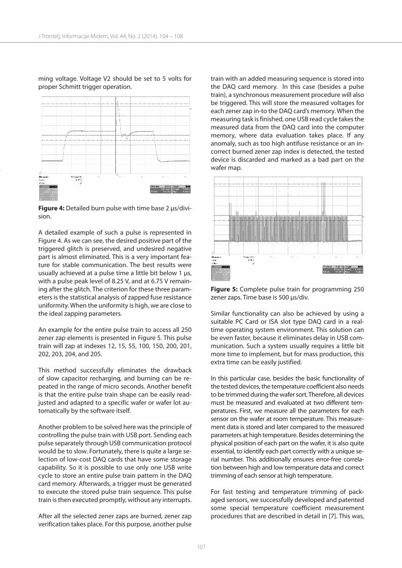
An example for the entire pulse train to access all 250 zener zap elements is presented in Figure 5. This pulse train will zap at indexes 12, 15, 55, 100, 150, 200, 201, 202, 203, 204, and 205.
This method successfully eliminates the drawback of slow capacitor recharging, and burning can be re-peated in the range of micro seconds. Another benefit is that the entire pulse train shape can be easily read-justed and adapted to a specific wafer or wafer lot au-tomatically by the software itself.
Another problem to be solved here was the principle of controlling the pulse train with USB port. Sending each pulse separately through USB communication protocol would be to slow. Fortunately, there is quite a large se-lection of low-cost DAQ cards that have some storage capability. So it is possible to use only one USB write cycle to store an entire pulse train pattern in the DAQ card memory. Afterwards, a trigger must be generated to execute the stored pulse train sequence. This pulse train is then executed promptly, without any interrupts.
After all the selected zener zaps are burned, zener zap verification takes place. For this purpose, another pulse
train with an added measuring sequence is stored into the DAQ card memory. In this case (besides a pulse train), a synchronous measurement procedure will also be triggered. This will store the measured voltages for each zener zap in-to the DAQ card’s memory. When the measuring task is finished, one USB read cycle takes the measured data from the DAQ card into the computer memory, where data evaluation takes place. If any anomaly, such as too high antifuse resistance or an in-correct burned zener zap index is detected, the tested device is discarded and marked as a bad part on the wafer map.
Figure 5: Complete pulse train for programming 250 zener zaps. Time base is 500 μs/div.
Similar functionality can also be achieved by using a suitable PC Card or ISA slot type DAQ card in a real-time operating system environment. This solution can be even faster, because it eliminates delay in USB com-munication. Such a system usually requires a little bit more time to implement, but for mass production, this extra time can be easily justified.
In this particular case, besides the basic functionality of the tested devices, the temperature coefficient also needs to be trimmed during the wafer sort. Therefore, all devices must be measured and evaluated at two different tem-peratures. First, we measure all the parameters for each sensor on the wafer at room temperature. This measure-ment data is stored and later compared to the measured parameters at high temperature. Besides determining the physical position of each part on the wafer, it is also quite essential, to identify each part correctly with a unique se-rial number. This additionally ensures error-free correla-tion between high and low temperature data and correct trimming of each sensor at high temperature.
For fast testing and temperature trimming of pack-aged sensors, we successfully developed and patented some special temperature coefficient measurement procedures that are described in detail in [7]. This was,
J Trontelj; Informacije Midem, Vol. 44, No. 2 (2014), 104 – 108

108
however, mainly used for the wafer sort procedure veri-fication and some small experimental series.
4 Conclusion
Most mixed-mode integrated circuits are dominated by a digital part area. Failure of a small analog section to meet strict, predefined accuracy requirements can have poor yield economics issues. Efficient trimming of criti-cal parameters is more than welcome - especially, when relatively large quantities of silicon are in question.
Next to yield, test time optimization is also very es-sential. With the described method, the trimming time of 250 zener zaps (without considering hardware de-pendent time for communication between DAQ and computer via USB port) takes app. 4 milliseconds. This time is actually determined by the reliability of the ‘on chip’ integrated communication protocol. The test sys-tem itself would be capable to accomplish the zapping task even faster.
Slightly more time is needed while doing the zener zapping verification. The reason for this is the required settling time for better zap resistance measuring ac-curacy. If we use 50 μs of time to settle the measure-ment for each zener zap, it takes app. 18 milliseconds to measure and verify the resistance of all 250 antifuses. Further test time optimization can be done by improv-ing the speed of the utilized communication protocol on the integrated circuit.
Besides an as short as possible test time, it is also very important feature to provide a low-cost multiplication of the test system. Several test sites usually drastically reduce the turn out time. For this particular project, six functional test sites were configured. To maintain the equivalence between the test sites, automatic test parameter calibration procedures were implemented. They also comply with strict automotive VDA 6.3 stand-ards. The entire wafer sort and the OTP process was ac-tually checked by external process audit, according to automotive VDA 6.3 (chapters 3-7) with a 92% overall degree of conformity.
At the time, when this article was written, approximate-ly ten million high sensitive integrated sensor circuits were trimmed and tested in our facilities. The test yield was more than 97%, while the yield difference between different test sites was negligible. The average number of OTP zener zaps per ASIC was approximately 36. This means that over the past few years (from 2009 to 2013) we have successfully burned and verified more than 360 million zener antifuses. Also, production was on-going when this article was written.
To briefly summarize, the most important contribution described in this article is a unique method for variable burn pulse generation that enables a very fast, reli-able, and highly adaptive zener zap burning and burn verification procedure for industrial application. This variability was also a key feature to do a rapid statistical analysis for fine tuning zener zapping parameters.
5 Acknowledgments
The author wishes to thank the staff of the Laboratory for Microelectronics at the University of Ljubljana for their help and support in this interesting project, which inspired him to write this article.
6 References
1. D. T. Comer, “Zener Zap Anti-Fuse Trim in VLSI Cir-cuits,” VLSI Design, Vol. 5, No. 1, pp. 89-100, 1996.
2. J. Teichmann, K. Burger, W. Hasche, J. Herrfurth, G. Täschner, “One-Time Programming (OTP) with Ze-ner Diodes in CMOS Processes,” 33rd European So-lid-State Device Research Conference – ESSDERC 2003, IEEE Catalog Number: 03EX704C, ISBN:0-7803-8100-0, pp. 433-435, 2003.
3. M. Chen, C. E. Huang, Y. H. Tseng, Y. C. King, C. J. Lin, “A New Antifuse Cell With Programmable Contact for Advance CMOS Logic Circuits,” Elec-tron Device Letters, IEEE, Vol. 29, No. 5, pp. 522-524, 2008.
4. R. Barsatan, T. Y. Man, M. Chan, “A zero-mask one-time programmable memory array for RFID ap-plications,” 2006 IEEE International Symposium on Circuits and Systems, ISCAS 2006, pp. 975-978, 2006.
5. J. Roig, J. Lebon, S. Vandeweghe, S. Mouhoubi, F. Bauwens, “Improved Current Filament Control during Zener Diode Zapping,” Special Issue 23rd European Symposium on the Reliability of Elec-tron Devices, Failure Physics and Analysis, Ca-gliary, Italy, pp. 2368-2373, 2012.
6. National Instruments, “DAQ M series User Manu-al,” 2008.
7. J. Trontelj Jr., J. Trontelj, B. Šmid, “Postopek in na-prava za testiranje in uravnavanje temperaturne-ga koeficienta integriranih vezij,” patent št. 24004, Urad Republike Slovenije za intelektualno lastni-no, 2013.
Arrived: 20. 01. 2014Accepted: 18. 03. 2014
J Trontelj; Informacije Midem, Vol. 44, No. 2 (2014), 104 – 108