family advanced t1/cept digital trunk pll · 2010-11-25 · figure 1 - functional block diagram f0i...
TRANSCRIPT

3-43
Features
• Provides T1 clock at 1.544 MHz locked to an 8kHz reference clock (frame pulse)
• Provides CEPT clock at 2.048 MHz and ST-BUSclock and timing signals locked to an internal orexternal 8 kHz reference clock
• Typical inherent output jitter (unfiltered)= 0.07UI peak-to-peak
• Typical jitter attenuation at: 10 Hz=23 dB,100Hz=43 dB, 5 to 40 kHz ≥ 64 dB
• Jitter-free “FREE-RUN” mode
• Uncommitted two-input NAND gate
• Low power CMOS technology
Applications
• Synchronization and timing control for T1and CEPT digital trunk transmission links
• ST- BUS clock and frame pulse source
Description
The MT8941 is a dual digital phase-locked loopproviding the timing and synchronization signals forthe T1 or CEPT transmission links and the ST-BUS.The first PLL provides the T1 clock (1.544 MHz)synchronized to the input frame pulse at 8 kHz. Thetiming signals for the CEPT transmission link and theST-BUS are provided by the second PLL locked to aninternal or an external 8 kHz frame pulse signal.
The MT8941 offers improved jitter performance overthe MT8940. The two devices also have somefunctional differences, which are listed in the sectionon “Differences between MT8941 and MT8940”.
Ordering Information
MT8941AE 24 Pin Plastic DIP (600 mil)MT8941AP 28 Pin PLCC
-40°C to +85 °C
Figure 1 - Functional Block Diagram
F0i
C12i
MS0
MS1
MS2
MS3
C8Kb
C16i
Ai
Bi
Yo VDD VSS RST
CVb
CV
ENCV
F0b
C4b
C4o
ENC4o
C2o
C2o
ENC2o
2:1 MUX
VariableClock
Control
ModeSelection
Logic
DPLL #2
InputSelector
ClockGenerator
Frame PulseControl
4.096 MHzClock
Control
2.048 MHzClock
Control
DPLL #1
ISSUE 5 July 1993
MT8941Advanced T1/CEPT Digital Trunk PLLCMOS ST-BUS FAMILY

MT8941 CMOS
3-44
Figure 2 - Pin Connections
Pin Description
Pin #Name Description
DIP PLCC
1 1 ENCV Variable clock enable (TTL compatible input) - This input directly controls the three statesof CV (pin 22) under all modes of operation. When HIGH, enables CV and when LOW, putsit in high impedance condition. It also controls the three states of CVb signal (pin 21) if MS1is LOW. When ENCV is HIGH, the pin CVb is an output and when LOW, it is in highimpedance state. However, if MS1 is HIGH, CVb is always an input.
2 2 MS0 Mode select ‘0’ input (TTL compatible) - This input in conjunction with MS1 (pin 4) selectsthe major mode of operation for both DPLLs. (Refer to Tables 1 and 2.)
3 3 C12i 12.352 MHz Clock input (TTL compatible) - Master clock input for DPLL #1.
4 6 MS1 Mode select-1 input (TTL compatible) - This input in conjunction with MS0 (pin 2) selectsthe major mode of operation for both DPLLs. (Refer to Tables 1 and 2.)
5 7 F0i Frame pulse input (TTL compatible) - This is the frame pulse input at 8 kHz. DPLL #1locks to the falling edge of this input to generate T1 (1.544 MHz) clock.
6 8 F0b Frame pulse Bidirectional (TTL compatible input and Totem-pole output) - Dependingon the minor mode selected for DPLL #2, it provides the 8 kHz frame pulse output or acts asan input to an external frame pulse.
7 9 MS2 Mode select-2 input (TTL compatible) - This input in conjunction with MS3 (pin 17) selectsthe minor mode of operation for DPLL #2. (Refer to Table 3.)
8 10 C16i 16.384 MHz Clock input (TTL compatible) - Master clock input for DPLL #2.
9 11 ENC4o Enable 4.096 MHz clock (TTL compatible input) - This active high input enables C4o (pin11) output. When LOW, the output C4o is in high impedance condition.
10 12 C8Kb Clock 8 kHz Bidirectional (TTL compatible input and Totem-pole output) - This is the 8kHz input signal on the falling edge of which the DPLL #2 locks during its NORMAL mode.When DPLL #2 is in SINGLE CLOCK mode, this pin outputs an 8 kHz internal signalprovided by DPLL #1 which is also connected internally to DPLL #2.
11 13 C4o Clock 4.096 MHz (Three state output) - This is the inverse of the signal appearing on pin13 (C4b) at 4.096 MHz and has a rising edge in the frame pulse (F0b) window. The highimpedance state of this output is controlled by ENC4o (pin 9).
12 14 VSS Ground (0 Volt)
28 PIN PLCC24 PIN PDIP
123456789
101112 13
141516
2423222120191817
ENVCMS0C12iMS1
F0iF0b
MS2C16i
ENC4oC8Kb
C4oVSS
VDDRSTCVCVbYoBiAiMS3ENC2oC2oC2oC4b
4
567891011
25242322212019
•
NC
NCCVbYoBiAiMS3ENC2o
NCMS1
F0iF0b
MS2C16i
ENC4o
C2o
3 2 1 28 27 26
12 13 14 15 16 17 18
C12
iM
S0
EN
CV
VD
DR
ST
CV
C8K
bC
4oV
SS
C4b
C2o NC

CMOS MT8941
3-45
13 15 C4b Clock 4.096 MHz- Bidirectional (TTL compatible input and Totem-pole output) - Whenthe mode select bit MS3 (pin 17) is HIGH, it provides the 4.096 MHz clock output with thefalling edge in the frame pulse (F0b) window. When pin 17 is LOW, C4b is an input to anexternal clock at 4.096 MHz.
14 16 C2o Clock 2.048 MHz (Three state output) - This is the divide by two output of C4b (pin 13) andhas a falling edge in the frame pulse (F0b) window. The high impedance state of this outputis controlled by ENC2o (pin 16).
15 17 C2o Clock 2.048 MHz (Three state output) - This is the divide by two output of C4b (pin 13) andhas a rising edge in the frame pulse (F0b) window. The high impedance state of this output iscontrolled by ENC2o (pin 16).
16 19 ENC2o Enable 2.048 MHz clock (TTL compatible input) - This active high input enables both C2oand C2o outputs (pins 14 and 15). When LOW, these outputs are in high impedancecondition.
17 20 MS3 Mode select 3 input (TTL compatible) - This input in conjunction with MS2 (pin 7) selectsthe minor mode of operation for DPLL #2. (Refer to Table 3.)
18,19
21,22
Ai, Bi Inputs A and B (TTL compatible) - These are the two inputs of the uncommitted NANDgate.
20 23 Yo Output Y (Totem pole output) - Output of the uncommitted NAND gate.
21 24 CVb Variable clock Bidirectional (TTL compatible input and Totem-pole output) - Whenacting as an output (MS1-LOW) during the NORMAL mode of DPLL #1, this pin provides the1.544 MHz clock locked to the input frame pulse F0i (pin 5). When MS1 is HIGH, it is aninput to an external clock at 1.544 MHz or 2.048 MHz to provide the internal signal at 8 kHzto DPLL #2.
22 26 CV Variable clock (Three state output) - This is the inverse output of the signal appearing onpin 21, the high impedance state of which is controlled by ENCV (pin 1).
23 27 RST Reset (Schmitt trigger input) - This input (active LOW) puts the MT8941 in its reset state.To guarantee proper operation, the device must be reset after power-up. The time constantfor a power-up reset circuit (see Figures 9-13) must be a minimum of five times the rise timeof the power supply. In normal operation, the RST pin must be held low for a minimum of60nsec to reset the device.
24 28 VDD VDD (+5V) Power supply.
4,5,
18, 25
NC No Connection.
Pin Description (continued)
Pin #Name Description
DIP PLCC

MT8941 CMOS
3-46
Functional Description
The MT8941 is a dual digital phase-locked loopproviding the timing and synchronization signals tothe interface circuits for T1 and CEPT (30+2)Primary Multiplex Digital Transmission links. Asshown in the functional block diagram (see Figure 1),the MT8941 has two digital phase-locked loops(DPLLs), associated output controls and the modeselection logic circuits. The two DPLLs, althoughsimilar in principle, operate independently to provideT1 (1.544 MHz) and CEPT (2.048 MHz) transmissionclocks and ST-BUS timing signals.
The principle of operation behind the two DPLLs isshown in Figure 3. A master clock is divided down to8 kHz where it is compared with the 8 kHz input, anddepending on the output of the phase comparison,the master clock frequency is corrected.
Figure 3 - DPLL Principle
The MT8941 achieves the frequency correction inboth directions by using three methods; speed-up,slow-down and no-correction.
As shown in Figure 4, the falling edge of the 8 kHzinput signal (C8Kb for DPLL #2 or F0i for DPLL # 1)is used to sample the internally generated 8 kHzclock and the correction signal (CS) once in everyframe (125 µs). If the sampled CS is “1”, then theDPLL makes a speed-up or slow-down correctiondepending upon the sampled value of the internal 8kHz signal. A sampled ”0” or “1” causes thefrequency correction circuit to respectively stretch orshrink the master clock by half a period at oneinstant in the frame. If the sampled CS is “0”, thenthe DPLL makes no correction on the master clockinput. Note that since the internal 8 kHz signal andthe CS signal are derived from the master clock, acorrection will cause both clocks to stretch or shrinksimultaneously by an amount equal to half the periodof the master clock.
Once in synchronization, the falling edge of thereference signal (C8Kb or F0i) will be aligned witheither the falling or the rising edge of CS. It is alignedwith the rising edge of CS when the reference signalis slower than the internal 8 kHz signal. On the otherhand, the falling edge of the
Figure 4 - Phase Comparison
reference signal will be aligned with the falling edgeof CS if the reference signal is faster than theinternal 8 kHz signal.
Input-to-Output Phase Relationship
The no-correction window size is 324 ns for DPLL #1and 32 µs for DPLL #2. It is possible for the relativephase of the reference signal to swing inside the no-correction window depending on its jitter and therelative drift of the master clock. As a result, thephase relationship between the input signal and theoutput clocks (and frame pulse in case of DPLL #2)may vary up to a maximum of window size. Thissituation is illustrated in Figure 4. The maximumphase variation for DPLL #1 is 324 ns and for DPLL#2 it is 32µs. However, this phase difference can beabsorbed by the input jitter buffer of Mitel’s T1/CEPTdevices.
The no-correction window acts as a filter for lowfrequency jitter and wander since the DPLL does nottrack the reference signal inside it. The size of theno-correction window is less than or equal to the sizeof the input jitter buffer on the T1 and CEPT devicesto guarantee that no slip will occur in the receivedT1/CEPT frame.
The circuit will remain in synchronization as long asthe input frequency is within the lock-in range of theDPLLs (refer to the section on “Jitter Performanceand Lock-in Range” for further details). The lock-inrange is wide enough to meet the CCITT line ratespecification (1.544 MHz ±32 ppm and 2.048 MHz±50 ppm) for the High Capacity Terrestrial DigitalService.
The phase sampling is done once in a frame (8 kHz)for each DPLL. The divisions are set at 8 and 193 forDPLL #1, which locks to the falling edge of the input
Master clock(12.352 MHz / 16.384 MHz)
FrequencyCorrection ÷ 8
Output
(1.544 MHz / 2.048 MHz)
Input (8 kHz) PhaseComparison
÷ 193 /÷ 256
C8Kb (DPLL #2)or F0i (DPLL #1) sampling edge
Interna l8 kHz
correction correctionCS speed-up
regionslow-down
regiontCS
tCSFno-correctionF0b(DPLL #2)
DPLL #1:DPLL #2:
tCSF = 766 × TP16
where, TP12 is the 12.352 MHz master clock oscillator periodfor DPLL #1 and TP16 is the 16.384 MHz master clock periodfor DPLL #2.
tCS = 4 × TP12 ± 0.5 × TP12
tCS = 512 × TP16 ± 0.5 × TP16

CMOS MT8941
3-47
at 8 kHz to generate T1 (1.544 MHz) clock. ForDPLL #2, the divisions are set at 8 and 256 toprovide the CEPT/ST-BUS clock at 2.048 MHzsynchronized to the falling edge of the input signal (8kHz). The master clock source is specified to be12.352 MHz for DPLL #1 and 16.384 MHz for DPLL#2 over the entire temperature range of operation.
The inputs MS0 to MS3 are used to select theoperating mode of the MT8941, see Tables 1 to 4.All the outputs are controlled to the high impedancecondition by their respective enable controls. Theuncommitted NAND gate is available for use inapplications involving Mitel’s MT8976/ MH89760 (T1Interfaces) and MT8979/MH89790 (CEPTInterfaces).
Modes of Operation
The operation of the MT8941 is categorized intomajor modes and minor modes. The major modesare defined for both DPLLs by the mode select pinsMS0 and MS1. The minor modes are selected bypins MS2 and MS3 and are applicable only to DPLL#2. There are no minor modes for DPLL #1.
Major modes of DPLL #1
DPLL #1 can be operated in three major modes asselected by MS0 and MS1 (Table 1). When MS1 isLOW, it is in NORMAL mode, which provides a T1(1.544 MHz) clock signal locked to the falling edgeof the input frame pulse F0i (8 kHz). DPLL #1requires a master clock input of 12.352 MHz (C12i).In the second and third major modes (MS1 is HIGH),DPLL #1 is set to DIVIDE an external 1.544 MHz or2.048 MHz signal applied at CVb (pin 21). Thedivision can be set by MS0 to be either 193 (LOW) or256 (HIGH). In these modes, the 8 kHz output atC8Kb is connected internally to DPLL #2, whichoperates in SINGLE CLOCK mode.
Major modes of DPLL #2
There are four major modes for DPLL #2 selectableby MS0 and MS1, as shown in Table 2. In all thesemodes DPLL #2 provides the CEPT PCM30 timing,and the ST-BUS clock and framing signals.
In NORMAL mode, DPLL #2 provides the CEPT/ST-BUS compatible timing signals locked to the fallingedge of the 8 kHz input signal (C8Kb). Thesesignals are 4.096 MHz (C4o and C4b) and 2.048MHz (C2o and C2o) clocks, and the 8 kHz framepulse (F0b) derived from the 16.384 MHz masterclock. This mode can be the same as the FREE-RUN mode if the C8Kb pin is tied to VDD or VSS.
Note: X: indicates don’t care
Table 1. Major Modes of DPLL #1
Table 2. Major Modes of DPLL #2
Table 3. Minor Modes of DPLL #2
In FREE-RUN mode, DPLL #2 generates the stand-alone CEPT and ST-BUS timing and framing signalswith no external inputs except the master clock set at16.384 MHz. The DPLL makes no correction in thisconfiguration and provides the timing signals withoutany jitter.
MS0
MS1
Mode ofOperation Function
X 0 NORMALProvides the T1 (1.544 MHz) clocksynchronized to the falling edge ofthe input frame pulse (F0i).
0 1 DIVIDE-1DPLL #1 divides the CVb input by193. The divided output isconnected to DPLL #2.
1 1 DIVIDE-2DPLL #1 divides the CVb input by256. The divided output isconnected to DPLL #2.
MS0
MS1
Mode ofOperation Function
0 0 NORMALProvides CEPT/ST-BUS timingsignals locked to the falling edge ofthe 8 kHz input signal at C8Kb.
1 0 FREE-RUNProvides CEPT/ST-BUS timing andframing signals with no externalinputs, except the master clock.
0 1 SINGLECLOCK-1
Provides CEPT/ST-BUS timingsignals locked to the falling edge ofthe 8 kHz internal signal provided byDPLL #1.
1 1 SINGLECLOCK-2
Provides CEPT/ST-BUS timingsignals locked to the falling edge ofthe 8 kHz internal signal provided byDPLL #1.
MS2
MS3
Functional Description
1 1Provides CEPT/ST-BUS 4.096 MHz and 2.048MHz clocks and 8kHz frame pulse depending onthe major mode selected.
0 1
Provides CEPT/ST-BUS 4.096 MHz & 2.048 MHzclocks depending on the major mode selectedwhile F0b acts as an input. However, the input onF0b has no effect on the operation of DPLL #2unless it is in FREE-RUN mode.
0 0
Overrides the major mode selected and acceptsproperly phase related external 4.096 MHz clockand 8 kHz frame pulse to provide the ST-BUScompatible clock at 2.048 MHz.
1 0
Overrides the major mode selected and accepts a4.096 MHz external clock to provide the ST-BUSclock and frame pulse at 2.048 MHz and 8 kHz,respectively.


CMOS MT8941
3-49
When MS3 is HIGH, DPLL #2 operates in any of themajor modes selected by MS0 and MS1. When MS3is LOW, it overrides the major mode selected andDPLL#2 accepts an external clock of 4.096 MHz onC4b (pin 13) to provide the 2.048 MHz clocks (C2oand C2o) and the 8 kHz frame pulse (F0b)compatible with the ST-BUS format. The mode selectbit MS2 controls the direction of the signal on F0b(pin 6).
When MS2 is LOW, the F0b pin is an 8 kHz framepulse input. This input is effective only when MS3 isalso LOW and pin C4b is fed by a 4.096 MHz clock,which has a proper phase relationship with thesignal on F0b (refer Figure 18). Otherwise, the inputon pin F0b will have no bearing on the operation ofDPLL #2, unless it is in FREE-RUN mode asselected by MS0 and MS1. In FREE-RUN mode,the input on F0b is treated the same way as theC8Kb input is in NORMAL mode. The frequency ofthe signal on F0b should be 16 kHz for DPLL #2 tolock and generate the ST-BUS compatible clocks at4.096 MHz and 2.048 MHz.
When MS2 is HIGH, the F0b pin provides the framepulse output compatible with the ST-BUS format andlocked to the internal or external input signal asdetermined by the other mode select pins.
Table 4 summarizes the modes of the two DPLL. Itshould be noted that each of the major modesselected for DPLL #2 can have any of the minormodes, although some of the combinations are
Table 5. Functions of the Bidirectional Signalsin Each Mode
Notes: i : Inputo : OutputX : “don’t care” input. Connect to VDD or VSS.
functionally similar. The required operation of bothDPLL #1 and DPLL #2 must be considered whendetermining MS0-MS3.
The direction and frequency of each of thebidirectional signals are listed in Table 5 for each ofthe given modes in Table 4.
Jitter Performance and Lock-in Range
The output jitter of a DPLL is composed of theintrinsic jitter, measured when no jitter is present atthe input, and the output jitter resulting from jitter onthe input signal. The spectrum of the intrinsic jitterfor both DPLLs of the MT8941 is shown in Figure 5.The typical peak-to-peak value for this jitter is0.07UI. The transfer function, which is the ratio ofthe output jitter to the input jitter (both measured at aparticular frequency), is shown in Figure 6 for DPLL#1 and Figure 7 for DPLL #2. The transfer function ismeasured when the peak-to-peak amplitude of thesinusoidal input jitter conforms to the following:
10 Hz - 100 Hz : 13.6 µs100 Hz - 10 kHz : 20 dB / decade roll-off> 10 kHz : 97.2 ns
The ability of a DPLL to phase-lock the input signalto the reference signal and to remain locked dependsupon its lock-in range. The lock-in range of the DPLLis specified in terms of the maximum frequencyvariation in the 8 kHz reference signal. It is alsodirectly affected by the oscillator frequencytolerance. Table 6 lists different values for the lock-inrange and the corresponding oscillator frequencytolerance for DPLL #1 and DPLL #2. The smallerthe tolerance value, the larger the lock-in range.
The T1 and CEPT standards specify that, for freerunning equipment, the output clock tolerance mustbe less than or equal to ±32ppm and ±50ppmrespectively. This requirement restricts the
Table 6. Lock-in Range vs. Oscillator FrequencyTolerance
* Please refer to the section on “Jitter Performance and Lock-inRange” for recommended oscillator tolerances for DPLL #1 & #2.
Mode#
F0b(kHz)
C4b(MHz)
C8Kb(kHz)
CVb(MHz)
0 i:8 i:4.096 i:X o:1.5441 i:X o:4.096 i:8 o:1.5442 o:8 i:4.096 i:X o:1.5443 o:8 o:4.096 i:8 o:1.5444 i:8 i:4.096 i:X i:1.5445 i:X o:4.096 o:8 i:1.5446 o:8 i:4.096 i:X i:1.5447 o:8 o:4.096 o:8 i:1.5448 i:8 i:4.096 i:X o:1.5449 i:16 o:4.096 i:X o:1.544
10 o:8 i:4.096 i:X o:1.54411 o:8 o:4.096 i:X o:1.54412 i:8 i:4.096 i:X i:2.40813 i:X o:4.096 o:8 i:2.40814 o:8 i:4.096 i:X i:2.40815 o:8 o:4.096 o:8 i:2.408
Oscillator Clock*Tolerance ( ±ppm)
Lock-in Range ( ±Hz)
DPLL #1 DPLL #25 2.55 1.91
10 2.51 1.8720 2.43 1.7932 2.33 1.6950 2.19 1.55
100 1.79 1.15150 1.39 .75175 1.19 .55

MT8941 CMOS
3-50
Figure 5- The Spectrum of the Inherent Jitter for either PLL
Figure 6 - The Jitter Transfer Function for PLL1
Figure 7 - The Jitter Transfer Function for PLL2

CMOS MT8941
3-51
oscillators of DPLL #1 and DPLL #2 to havemaximum tolerances of ±32ppm and ±50ppmrespectively.
However, if DPLL #1 and DPLL #2 are daisy-chainedas shown in Figures 9 and 10, the output clocktolerance of DPLL #1 will be equal to that of theDPLL #2 oscillator when DPLL #2 is free-running. Inthis case, the oscillator tolerance of DPLL #1 has noimpact on its output clock tolerance. For this reason,
it is recommended to use a ±32 ppm oscillator forDPLL #2 and a ±100 ppm oscillator for DPLL #1.
Differences between MT8941 and MT8940
The MT8941 and MT8940 are pin and modecompatible for most applications. However, the usershould take note of the following differences betweenthe two parts.
Figure 8 - Application Differences between the MT8940 and MT8941
a) Distributed Timing
MUX
MT8940
MT8940
8 kHz Reference Signal
8 kHz Reference Signal
Line Card 1
Clocks
Line Card n
Clocks
Data Bus
Line Card 1
Line Card n
MT8941
MUX
8 kHz Reference Signal
8 kHz Reference Signal
Clocks
b) Centralized TimingData Bus
MT8941 CMOS
3-52
Besides the improved jitter performance, theMT8941 differs from the MT8940 in three otherareas:
1. Input pins on the MT8941 do not incorporateinternal pull-up or pull-down resistors. Inaddition, the output configuration of thebidirectional C8Kb pin has been converted froman open drain output to a Totem-pole output.
2. The MT8941 includes a no-correction window tofilter out low frequency jitter and wander asillustrated in Figure 4. Consequently, there is noconstant phase relationship between referencesignal F0i of DPLL # 1 or C8Kb of DPLL #2 andthe output clocks of DPLL #1 or DPLL #2.Figure 4 shows the new phase relationshipbetween C8Kb and the DPLL #2 output clocks.Figure 8 illustrates an application where theMT8941 cannot replace the MT8940 andsuggests an alternative solution.
3. The MT8941 must be reset after power-up inorder to guarantee proper operation, which is notthe case for the MT8940.
4. For the MT8941, DPLL #2 locks to the fallingedge of the C8Kb reference signal. DPLL#2 ofthe MT8940 locks on to the rising edge of C8Kb.
5. While the MT8940 is available only in a 24 pinplastic DIP, the MT8941 has an additional 28 pinPLCC package option.
Applications
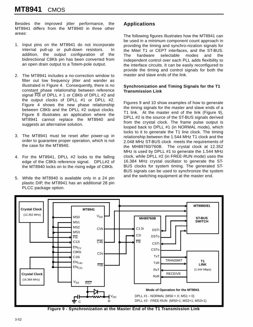
The following figures illustrates how the MT8941 canbe used in a minimum component count approach inproviding the timing and synchro-nization signals forthe Mitel T1 or CEPT interfaces, and the ST-BUS.The hardware selectable modes and theindependent control over each PLL adds flexibility tothe interface circuits. It can be easily reconfigured toprovide the timing and control signals for both themaster and slave ends of the link.
Synchronization and Timing Signals for the T1Transmission Link
Figures 9 and 10 show examples of how to generatethe timing signals for the master and slave ends of aT1 link. At the master end of the link (Figure 9),DPLL #2 is the source of the ST-BUS signals derivedfrom the crystal clock. The frame pulse output islooped back to DPLL #1 (in NORMAL mode), whichlocks to it to generate the T1 line clock. The timingrelationship between the 1.544 MHz T1 clock and the2.048 MHz ST-BUS clock meets the requirements ofthe MH89760/760B. The crystal clock at 12.352MHz is used by DPLL #1 to generate the 1.544 MHzclock, while DPLL #2 (in FREE-RUN mode) uses the16.384 MHz crystal oscillator to generate the ST-BUS clocks for system timing. The generated ST-BUS signals can be used to synchronize the systemand the switching equipment at the master end.
Figure 9 - Synchronization at the Master End of the T1 Transmission Link
Crystal Clock
(16.384 MHz)
Crystal Clock
(12.352 MHz)
MT8941
MS0
MS1
MS2
MS3
F0iC12i
ENCV
C8Kb
C16i
ENC4o
ENC2o
VSS
VDD
CVb
C4b
C2o
F0b
RST
MH89760B
C1.5i
C2i
F0i
DSTi
DSTo
CSTi
CSTo
TxT
TxR
RxT
RxR
MT8980/81
ST-BUSSWITCH
T1LINK
(1.544 Mbps)
TRANSMIT
RECEIVE
Mode of Operation for the MT8941
DPLL #1 - NORMAL (MS0 = X; MS1 = 0)DPLL #2 - FREE-RUN (MS0=1; MS2=1; MS3=1)
VDD
RC

CMOS MT8941
3-53
Figure 10 - Synchronization at the Slave End of the T1 Transmission Link
Figure 11 - Synchronization at the Master End of the CEPT Digital Transmission Link
Crystal Clock
(16.384 MHz)
Crystal Clock
(12.352 MHz)
MT8941
MS0
MS1
MS2MS3
F0iC12i
ENCV
C8Kb
C16i
ENC4o
ENC2o
VSS
VDD
CVb
C4b
C2o
F0b
RST
MH89760B
C1.5i
C2i
F0i
DSTi
DSTo
CSTi
CSTo
TxT
TxR
RxT
RxR
MT8980/81
ST-BUSSWITCH
T1LINK
(1.544 Mbps)
TRANSMIT
RECEIVE
Mode of Operation for the MT8941
DPLL #1 - NORMAL ( MS1=0)DPLL #2 - NORMAL (MS0=0; MS1=0; MS2=1; MS3=1)VDD
RC
E8Ko
Crystal Clock
(16.384 MHz)
MT8941
MS0
MS1
MS2
MS3
F0iC12i
ENCV
C8Kb
C16i
ENC4o
ENC2o
VSS
VDD
C4b
C2o
F0b
Yo
RST
TRANSMIT
RECEIVE
MT8980/81
ST-BUSSWITCH
MH89790B
C2i
F0i
DSTi
DSTo
CSTi0
CSTo
RxT
RxR
Mode of Operation for the MT8941
DPLL #1 - NOT USEDDPLL #2 - FREE-RUN (MS0=1; MS1=0; MS2=1; MS3=1)
CSTi1
OUTA
OUTB
VDDRC
CEPTPRIMARY
MULTIPLEXDIGITAL
LINK
At the slave end of the link (Figure 10) both theDPLLs are in NORMAL mode, with DPLL #2providing the ST-BUS timing signals locked to the 8kHz frame pulse (E8Ko) extracted from the receivedsignal on the T1 line. The regenerated frame pulseis looped back to DPLL #1 to provide the T1 lineclock, which is the same as the master end.
The 12.352 MHz and 16.384 MHz crystal clocksources are necessary for DPLL #1 and #2,respectively.
Synchronization and Timing Signals for theCEPT Transmission Link
The MT8941 can be used to provide the timing andsynchronization signals for the MH89790/790B,Mitel’s CEPT (30+2) Digital Trunk Interface Hybrid.Since the operational frequencies of the ST-BUS andthe CEPT primary multiplex digital trunk are thesame, only DPLL #2 is required.

MT8941 CMOS
3-54
Figure 12 - Synchronization at the Slave End of the CEPT Digital Transmission Link
Crystal Clock
(16.384 MHz)
MT8941
MS0
MS1
MS2MS3
F0iC12i
ENCV
C8Kb
C16iENC4oENC2o
VSS
VDD
C4b
C2o
F0b
Yo
RST
VDDRC
MH89790B
C2i
F0i
DSTi
DSTo
CSTi0
CSTo
RxT
RxR
CSTi1
OUTA
OUTB
MT8980/81
ST-BUSSWITCH
TRANSMIT
RECEIVE
Mode of Operation for the MT8941
DPLL #1 - NOT USEDDPLL #2 - NORMAL (MS0=0; MS1=0; MS2=1; MS3=1)
CEPTPRIMARY
MULTIPLEXDIGITAL
LINK
E8Ko
Figures 11 and 12 show how the MT8941 can beused to synchronize the ST-BUS to the CEPTtransmission link at the master and slave ends.
Generation of ST-BUS Timing Signals
The MT8941 can source the properly formatted ST-BUS timing and control signals with no externalinputs except the crystal clock. This can be used asthe standard timing source for ST-BUS systems orany other system with similar clock requirements.
Figure 13 shows two such applications using DPLL#2. In one case, the MT8941 is in FREE-RUNmode with an oscillator input of 16.384 MHz. In theother case, it is in NORMAL mode with the C8Kbinput tied to VDD. For these applications, DPLL #2does not make any corrections and therefore, theoutput signals are free from jitter. DPLL #1 iscompletely free.
For prototyping purposes, Mitel offers the MT8941Crystal Kit (MB6022) which contains 16.384 MHzand 12.352 MHz clock oscillators.
Figure 13 - Generation of the ST-BUS Timing Signals
Crystal Clock(16.384 MHz)
MT8941
MS0
MS1MS2MS3
F0iC12i
ENCVC8KbC16iENC4oENC2oAiBi
VSS
VDD
C4b
RST
C4o
C2o
C2o
F0b
ST-BUS
TIMING
SIGNALS
DPLL #1 - NOT USEDDPLL #2 - NORMAL MODE(MS0=0; MS1=0;MS2=1; MS3=1)
VDDRC
MT8941
MS0
MS1MS2MS3
F0iC12i
ENCVC8KbC16iENC4oENC2oAiBi
VSS
VDD
C4b
RST
C4o
C2o
C2o
F0b
DPLL #1 - NOT USEDDPLL #2 - FREE-RUN MODE(MS0=1; MS1=0;MS2=1;MS3=1)
Crystal Clock(16.384 MHz)
VDDRC
ST-BUS
TIMING
SIGNALS

CMOS MT8941
3-55
* Exceeding these values may cause permanent damage. Functional operation under these conditions is not implied.
‡ Typical figures are at 25°C and are for design aid only: not guaranteed and not subject to production testing.
‡ Typical figures are at 25°C and are for design aid only: not guaranteed and not subject to production testing.
Absolute Maximum Ratings* - Voltages are with respect to ground (VSS) unless otherwise stated.
Parameter Symbol Min Max Units
1 Supply Voltage VDD -0.3 7.0 V
2 Voltage on any pin VI VSS-0.3 VDD+0.3 V
3 Input/Output Diode Current IIK/OK ±10 mA
4 Output Source or Sink Current IO ±25 mA
5 DC Supply or Ground Current IDD/ISS ±50 mA
6 Storage Temperature TST -55 125 oC
7 Package Power Dissipation Plastic DIPPLCC
PDPD
1200600
mWmW
Recommended Operating Conditions - Voltages are with respect to ground (VSS) unless otherwise stated.
Characteristics Sym Min Typ ‡ Max Units Test Conditions
1 Supply Voltage VDD 4.5 5.0 5.5 V
2 Input HIGH Voltage VIH 2.0 VDD V
3 Input LOW Voltage VIL VSS 0.8 V
4 Operating Temperature TA -40 25 85 oC
DC Electrical Characteristics - Voltages are with respect to ground (VSS) unless otherwise stated.
VDD=5.0V±5%; VSS=0V; TA=-40 to 85°C.
Characteristics Sym Min Typ ‡ Max Units Test Conditions
1SUP
Supply CurrentIDD 8 15 mA Under clocked condition, with the
inputs tied to the same supplyrail as the corresponding pull-up/down resistors.
2
IN
Input HIGH voltage (For all theinputs except pin 23)
VIH 2.0 V
3 Positive-going thresholdvoltage (For pin 23)
V+ 3.0 4.0 V
4 Input LOW voltage (For all theinputs except pin 23)
VIL 0.8 V
5 Negative-going thresholdvoltage (For pin 23)
V- 1.0 1.5 V
6 OUT
Output current HIGH IOH -4 mA VOH=2.4 V
7 Output current LOW IOL 4 mA VOL=0.4 V
8 Leakage current on bidirect-ional pins and all inputs exceptC12i, C16i, RST, MS1, MS0
IIL -100 -30 -8 µA VIN=VSS
9 Leakage current on pins MS1,MS0
IIL 10 35 120 µA VIN=VDD
10 Leakage current on all three-state outputs and C12i, C16i,RST inputs
IIL -10 ±1 +10 µA VI/O=VSS or VDD
MT8941 CMOS
3-56
† Timing is over recommended temperature & power supply voltages.‡ Typical figures are at 25°C and are for design aid only: not guaranteed and not subject to production testing.
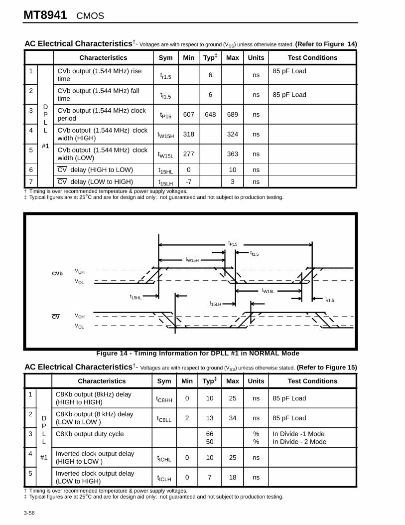
Figure 14 - Timing Information for DPLL #1 in NORMAL Mode
† Timing is over recommended temperature & power supply voltages.‡ Typical figures are at 25°C and are for design aid only: not guaranteed and not subject to production testing.
AC Electrical Characteristics †- Voltages are with respect to ground (VSS) unless otherwise stated. (Refer to Figure 14)
Characteristics Sym Min Typ ‡ Max Units Test Conditions
1
DPLL
#1
CVb output (1.544 MHz) risetime
tr1.5 6 ns85 pF Load
2 CVb output (1.544 MHz) falltime
tf1.5 6 ns 85 pF Load
3 CVb output (1.544 MHz) clockperiod
tP15 607 648 689 ns
4 CVb output (1.544 MHz) clockwidth (HIGH)
tW15H 318 324 ns
5 CVb output (1.544 MHz) clockwidth (LOW)
tW15L 277 363 ns
6 CV delay (HIGH to LOW) t15HL 0 10 ns
7 CV delay (LOW to HIGH) t15LH -7 3 ns
AC Electrical Characteristics †- Voltages are with respect to ground (VSS) unless otherwise stated. (Refer to Figure 15)
Characteristics Sym Min Typ ‡ Max Units Test Conditions
1
DPLL
#1
C8Kb output (8kHz) delay(HIGH to HIGH)
tC8HH 0 10 25 ns 85 pF Load
2 C8Kb output (8 kHz) delay(LOW to LOW )
tC8LL 2 13 34 ns 85 pF Load
3 C8Kb output duty cycle 6650
%%
In Divide -1 ModeIn Divide - 2 Mode
4 Inverted clock output delay(HIGH to LOW )
tICHL 0 10 25 ns
5 Inverted clock output delay(LOW to HIGH)
tICLH 0 7 18 ns
CVb
CV
VOH
VOL
VOH
VOL
tf1.5
t15HLt15LH
tr1.5
tP15
tW15H
tW15L
CMOS MT8941
3-57
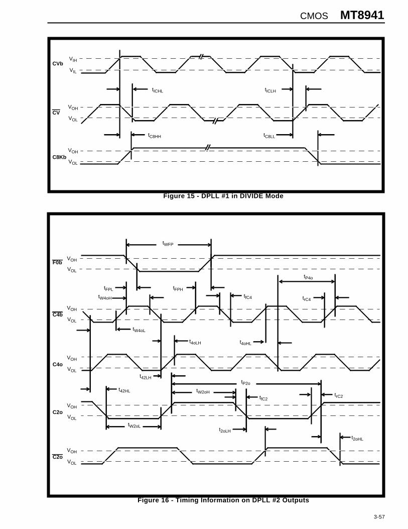
Figure 15 - DPLL #1 in DIVIDE Mode
Figure 16 - Timing Information on DPLL #2 Outputs
VOH
VOL
VOH
VOL
VOH
VOL
VOH
VOL
VOH
VOL
F0b
C4b
C4o
C2o
C2o
tFPL tFPH
tfC4 trC4
t4oLH t4oHL
t42LH
t42HL
tfC2trC2
t2oLH
t2oHL
tWFP
tP2o
tW2oH
tW2oL
tW4oH
tW4oL
tP4o
CVb
CV
C8Kb
VIH
VIL
VOH
VOL
VOH
VOL
tICHL tICLH
tC8HH tC8LL
MT8941 CMOS
3-58
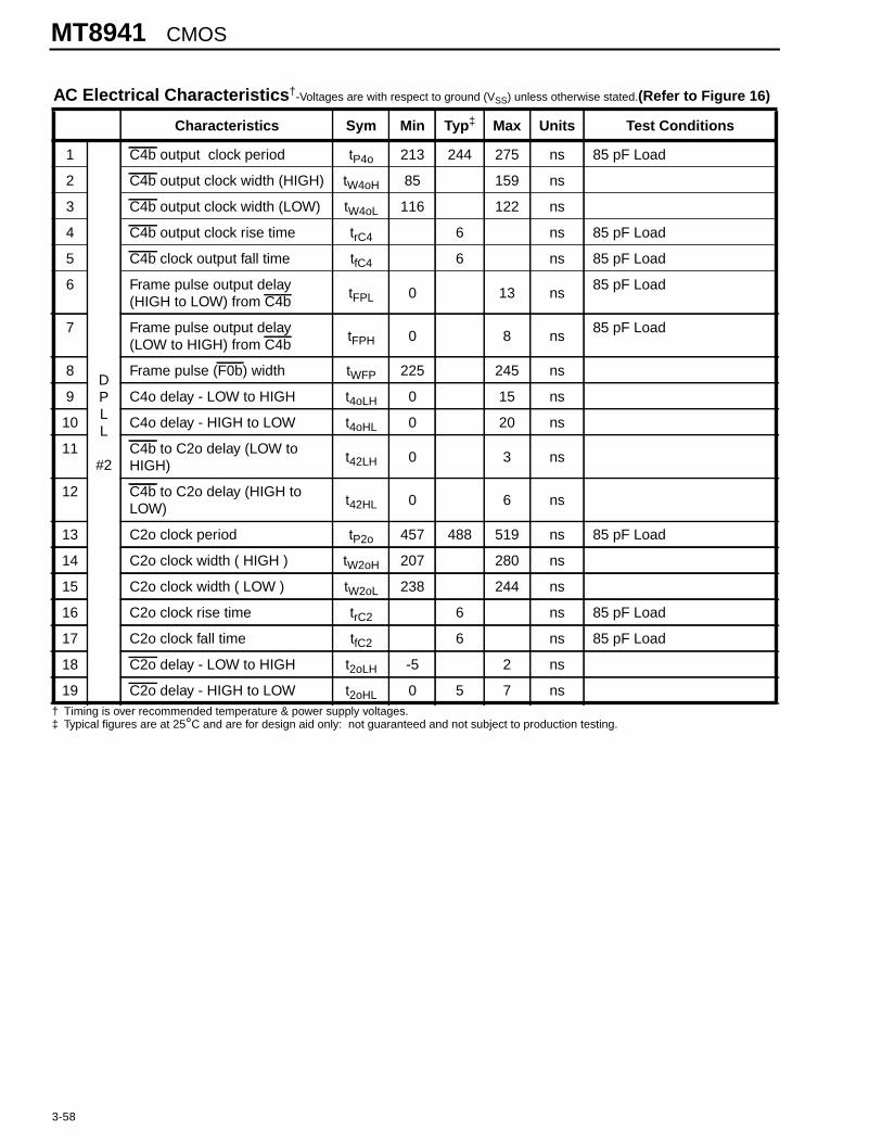
† Timing is over recommended temperature & power supply voltages.‡ Typical figures are at 25°C and are for design aid only: not guaranteed and not subject to production testing.
AC Electrical Characteristics †-Voltages are with respect to ground (VSS) unless otherwise stated.(Refer to Figure 16)
Characteristics Sym Min Typ ‡ Max Units Test Conditions
1
DPLL
#2
C4b output clock period tP4o 213 244 275 ns 85 pF Load
2 C4b output clock width (HIGH) tW4oH 85 159 ns
3 C4b output clock width (LOW) tW4oL 116 122 ns
4 C4b output clock rise time trC4 6 ns 85 pF Load
5 C4b clock output fall time tfC4 6 ns 85 pF Load
6 Frame pulse output delay(HIGH to LOW) from C4b
tFPL 0 13 ns85 pF Load
7 Frame pulse output delay(LOW to HIGH) from C4b
tFPH 0 8 ns85 pF Load
8 Frame pulse (F0b) width tWFP 225 245 ns
9 C4o delay - LOW to HIGH t4oLH 0 15 ns
10 C4o delay - HIGH to LOW t4oHL 0 20 ns
11 C4b to C2o delay (LOW toHIGH)
t42LH 0 3 ns
12 C4b to C2o delay (HIGH toLOW)
t42HL 0 6 ns
13 C2o clock period tP2o 457 488 519 ns 85 pF Load
14 C2o clock width ( HIGH ) tW2oH 207 280 ns
15 C2o clock width ( LOW ) tW2oL 238 244 ns
16 C2o clock rise time trC2 6 ns 85 pF Load
17 C2o clock fall time tfC2 6 ns 85 pF Load
18 C2o delay - LOW to HIGH t2oLH -5 2 ns
19 C2o delay - HIGH to LOW t2oHL 0 5 7 ns
CMOS MT8941
3-59
† Timing is over recommended temperature & power supply voltages.‡ Typical figures are at 25°C and are for design aid only: not guaranteed and not subject to production testing.* Please review the section on "Jitter Performance and Lock-in Range".
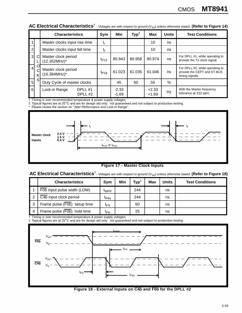
Figure 17 - Master Clock Inputs
† Timing is over recommended temperature & power supply voltages.‡ Typical figures are at 25°C and are for design aid only: not guaranteed and not subject to production testing.
Figure 18 - External Inputs on C4b and F0b for the DPLL #2
AC Electrical Characteristics † - Voltages are with respect to ground (VSS) unless otherwise stated. (Refer to Figure 14)
Characteristics Sym Min Typ ‡ Max Units Test Conditions
1
CLOCKS
Master clocks input rise time tr 10 ns
2 Master clocks input fall time tf 10 ns
3 Master clock period(12.352MHz)*
tP12 80.943 80.958 80.974 nsFor DPLL #1, while operating toprovide the T1 clock signal.
4 Master clock period(16.384MHz)*
tP16 61.023 61.035 61.046 nsFor DPLL #2, while operating toprovide the CEPT and ST-BUStiming signals.
5 Duty Cycle of master clocks 45 50 55 %
6 Lock-in Range DPLL #1DPLL #2
-2.33-1.69
+2.33+1.69
HzWith the Master frequencytolerance at ±32 ppm.
AC Electrical Characteristics †- Voltages are with respect to ground (VSS) unless otherwise stated. (Refer to Figure 18)
Characteristics Sym Min Typ ‡ Max Units Test Conditions
1 F0b input pulse width (LOW) tWFP 244 ns
2 C4b input clock period tP4o 244 ns
3 Frame pulse (F0b) setup time tFS 50 ns
4 Frame pulse (F0b) hold time tFH 25 ns
Master clock
inputs
2.4 V1.5 V0.4 V
tr tf
tP12 or tP16
F0b
C4b
VIH
VIL
VIH
VIL
tFS
tWFP
tFH
tP4o

MT8941 CMOS
3-60
† Timing is over recommended temperature & power supply voltages.‡ Typical figures are at 25°C and are for design aid only: not guaranteed and not subject to production testing.
Figure 19 - Three State Outputs and Enable Timings
† Timing is over recommended temperature & power supply voltages.‡ Typical figures are at 25°C and are for design aid only: not guaranteed and not subject to production testing.
AC Electrical Characteristics †- Voltages are with respect to ground (VSS) unless otherwise stated. (Refer to Figure 19)
Characteristics Sym Min Typ ‡ Max Units Test Conditions
1
OUTPUT
Delay from Enable to Output(HIGH to THREE STATE)
tPHZ 16 ns 85 pF Load
2 Delay from Enable to Output(LOW to THREE STATE)
tPLZ 12 ns 85 pF Load
3 Delay from Enable to Output(THREE STATE to HIGH)
tPZH 11 ns 85 pF Load
4 Delay from Enable to Output(THREE STATE to LOW)
tPZL 50 16 ns 85 pF Load
AC Electrical Characteristics † - Uncommitted NAND GateVoltages are with respect to ground (VSS) unless otherwise stated.
Characteristics Sym Min Typ ‡ Max Units Test Conditions
1 Propagation delay (LOW toHIGH), input Ai or Bi to output
tPLH 11 ns 85 pF Load
2 Propagation delay (HIGH toLOW), input Ai or Bi to output
tPHL 15 ns 85 pF Load
EnableInput
OutputLOW toOFF
OutputHIGHto OFF
10%
90%
1.3 V
1.3 V
OutputsEnabled
OutputsEnabled
OutputsDisabled
tPLZ
tPHZ
tPZL
tPZH
tf 6 ns tr 6 ns3.0 V2.7 V1.3 V0.3 V


www.zarlink.com
Information relating to products and services furnished herein by Zarlink Semiconductor Inc. trading as Zarlink Semiconductor or its subsidiaries (collectively“Zarlink”) is believed to be reliable. However, Zarlink assumes no liability for errors that may appear in this publication, or for liability otherwise arising from theapplication or use of any such information, product or service or for any infringement of patents or other intellectual property rights owned by third parties which mayresult from such application or use. Neither the supply of such information or purchase of product or service conveys any license, either express or implied, underpatents or other intellectual property rights owned by Zarlink or licensed from third parties by Zarlink, whatsoever. Purchasers of products are also hereby notifiedthat the use of product in certain ways or in combination with Zarlink, or non-Zarlink furnished goods or services may infringe patents or other intellectual propertyrights owned by Zarlink.
This publication is issued to provide information only and (unless agreed by Zarlink in writing) may not be used, applied or reproduced for any purpose nor form partof any order or contract nor to be regarded as a representation relating to the products or services concerned. The products, their specifications, services and otherinformation appearing in this publication are subject to change by Zarlink without notice. No warranty or guarantee express or implied is made regarding thecapability, performance or suitability of any product or service. Information concerning possible methods of use is provided as a guide only and does not constituteany guarantee that such methods of use will be satisfactory in a specific piece of equipment. It is the user’s responsibility to fully determine the performance andsuitability of any equipment using such information and to ensure that any publication or data used is up to date and has not been superseded. Manufacturing doesnot necessarily include testing of all functions or parameters. These products are not suitable for use in any medical products whose failure to perform may result insignificant injury or death to the user. All products and materials are sold and services provided subject to Zarlink’s conditions of sale which are available on request.
Purchase of Zarlink’s I2C components conveys a licence under the Philips I2C Patent rights to use these components in an I2C System, provided that the systemconforms to the I2C Standard Specification as defined by Philips.
Zarlink and the Zarlink Semiconductor logo are trademarks of Zarlink Semiconductor Inc.
Copyright 2002, Zarlink Semiconductor Inc. All Rights Reserved.
TECHNICAL DOCUMENTATION - NOT FOR RESALE
For more information about all Zarlink productsvisit our Web Site at