faculty of engineering - near east universitydocs.neu.edu.tr/library/4825566717.pdf · faculty of...
TRANSCRIPT

---·~ - ~·-- ------
NEAR EAST UNIVERSITY
Faculty of Engineering
Department of Electrical and Electronic Engineering
OPTICAL COMMUNICATION
Graduation Project EE- 400
Student: Aneel Shahzad Baig (971305)
Supervisor: Prof. Dr. Fakhreddin Mamedov
Nicosia - 2001 f

ACKNOWLEDGMENT
I wish to thank to my parents who supported and encouraged me at every stage
of my education and who still being generous for me as they are ever.
My sincere thanks and appreciation for my supervisor Prof. Dr. Fakhreddin
Mamedov who was very generous with his help, valuable advices and comments to
accomplish this research and who will be always my respectful teacher.
All my thanks goes to N.E.U. educational staff especially to electrical &
electronic engineering teaching staff for their generosity and special concern of me and
all E.E. students.
Final acknowledgments go to my class mates and friends Kashif, Umair, Zubair,
Salman, Usman and Taufiq who provided me with their valuable suggestions
throughout the completion ofmy project.
ABSTRACT
A communication network consists of interconnected links, each of which has
three basic elements: transmitter, channel and receiver. An optical fiber consists of a
core and a cladding layer. According to core diameters there are single mode and
multimode fibers. Fiber attenuation and dispersion limit the transmission capacity and
distance. Attenuation is caused by photon absorption, scattering, fiber bending and
coupling. Different propagation velocities of components in the lightwave cause fiber
dispersion.
Photdetectors convert incident light into current from photon absorption and
electron hole pair (EHP) generation. Noise and distortion are important performance
limiting factors in signal detection. Thermal noise is white Gaussian noise due to
random thermal radiations. Shot noise is caused by random EHP generations in
photodiodes. APD noise is due to both random primary an secondary EHP generations.
RIN is caused by intensity fluctuation. Phase noise is the phase fluctuation. Mode
partition noise is caused by random power distribution among longitudinal modes.
Transmission performance in digital communications is measured by the BER, which is
in turn determined by the received signal power, noise power, intersymbol interference
and crosstalk.
In time domain medium access, stations send data over different time intervals.
In TDMA time is divided into frames, which are fixed in size. TDM has fixed frame
size consisting of the overhead and fixed number of slots. WDoMA systems differ in
various aspects. According to the relative size between channel separation and
bandwidth. WDoMA systems are either dense or sparse. There is WDM, where signals
from set of transmitters are multiplexed for transmission over a long distance. Photonic
switching can avoid the electronics speed bottleneck by providing optical domain
switching. A photonic switch needs to be able to configure optical paths according to
the traffic patterns. External modulation is used to modulate the refractive index of a
waveguide through which a constant frequency lightwave passes. In contrast to direct
detection, coherent detection has the capability to detect the phase, frequency, amplitude
and even the polarization of the incident light signal. When transmission system power
is limited, optical amplifiers are used to improve the received SNR and increase the
repeater distance .
••
11

INTRODUCTION
In this project optical communications is studied with intensive care. Optical
communication is a new technology, which will have a large impact on
telecommunications as well as fast data transmission and computer interconnections.
The project consists of five chapters.
Chapter 1 gives a short introduction to optical communications by considering
the historical development, the general system and the major advantages provided by
this technology.
Chapter 2 gives the basic idea of a communication system and a communication
network. Important elements in the communication process are introduced, which
consist of Light sources, Optical Fibers, and Light Detection devices.
Chapter 3 will cover important and advanced topics in optical communications.
On the transmitter side direct modulation is discussed in detail. On the receiver side
Coherent Detection and timing recovery are explained. Finally, on the subject of light
signal transmission technology, recent technology developments on optical amplifiers
are discussed. These recent breakthroughs were developed to overcome the transmission
loss and dispersion problems over a very long distance. It evaluates the important aspect
of signal transmission, which is noise analysis. It also gives the brief idea of Noise and
Distortion, their Reduction Techniques, Shot Noise in Pin Diodes, Relative intensity
noise in Laser Diodes, Other types of noise and Total Noise of a system.
Chapter 4 covers the important Optical Networking aspects and supporting
optical devices. Specifically, various multiplexing and switching techniques in optical
communication are explained, and various innovative devices are described .
•
ill

TABLE OF CONTENTS
ACKNOWLEDGMENT
ABSTRACT
INTRODUCTION
II
iii
1. INTRODUCTION TO OPTICAL COMMUNICATIONS 1
1.1 Introduction
1.2 Communication Systems
1.3 Baseband versus Passband
1.4 Analog versus Digital
1.5 Coherent versus Incoherent
1.6 Modulation and Line Coding
1. 7 Advantages of Optical Communications 1.7.1 Large Transmission Capacity
1.7.2 Low Loss
1.7.3 Immunity to Interface
1.7.4 High-Speed Interconnections
1. 7.5 ParaHel Transmission
1
2
4
4
5
5
5
5
6
6
6
6
7
7
7
8
11
14
16
20
21
23
27
27
28
2. OPTICAL COMMUNICATION DEVICES
2.1 Light Sources
2.1.1 Semiconductor Light Sources
2.1.2 Light Emitting Diodes
2.1.3 Laser Principles
2.1.4 Fabry-Perot Laser Diodes
2.1.5 Single Mode Laser
2.2 Optical Fibers
2.2.1 Structure and Types
2.2.2 Light Propagation in Fiper Optics
2.3 Light Detection
2.3.1 Photoconductors
2.3.2 Photodiodes
3. SIGNAL PROCESSING 29
3.1 Direct Modulation 29
3.1.1 Direct Modulation for LEDs 30
3.1.2 Rate Equation for Laser Diodes 35
3.1.3 Pulse Input Response for Laser Diodes 37
3.1.4 Small Signal Response for Laser Diodes 38
3.2 External Modulation 38
3.2.1 Principles of External Modulation 39
3.2.2 Wave Propagation in Anisotropic Media 39
3.2.3 Electro-Optic Modulation 41
3.2.4 Acousto-Optic Modulation 43
3.3 Coherent Detection 44
3.3.1 Signal and Noise Formulation 44
3.3.2 On-Off Keying 46
3.3.3 Phase-Shift Keying 48
3.3.4 Differential Phase-Shift Keying 48
3.3.5 Frequency-Shift Keying 49
3.3.6 Polarization-Shift Keying 50
3.4 Incoherent Detection 50
3.4.1 - Analog Signal Detection 50
3.4.2 Binary Digital Signal Detection 51
3.4.3 Intersymbol Interference and Noise Formulation 52
3.4.4 Bit Error Rate Neglecting Intersymbol Interference 53
3.4.5 Bit Error Rate Including Intersymbol Interference 53
3.5 Optical Amplification 54
3.5.1 Semiconductor Amplifiers 54
3.6 Noise in Optical Communication 56
3.6.1 Effects Of Noise and Distortion 57
3.6.2 Noise and Distortion Reduction Techniques 59
3.6.3 Shot Noise from Pin Diodes 62
3.6.4 Thermal Noise 62
3.6.5 Relative Intensity Noise in Laser Diodes 64
3.6.6 Phase Noise from Laser Diodes 64
3.6.7 Mode Partition Noise 66
3.6.8 Avalanche Noise in A.PDs 68
3.6.9 Noise from Optical Amplification 68
3.6.10 Total Noise 68
4. NETWORKING 70
4.1 Time-Domain Medium Access 70
4.1.1 Time-Division Multiple Access 71
4.1.2 Optical-Domain TDMA 74
4.1.3 Time-Division Multiplexing 76
4.2 Wavelength-Domain Medium Access 77
4.2.1 Wavelength-Division Multiple Access 78
4.2.2 Tunable Sources 79
4.2.3 Frequency Independent Coupling 81
4.2.4 Frequency Dependent Multiplexing 81
4.2.5 De-Multiplexing and Optical Filtering 82
4.3 Photonic Switching 83
4.3.1 Switching Architectures 84
4.3.2 Spatial-Domain Photonic Switching 86
4.3.3 Multidimensional Photonic Switching 87
CONCLUSION 90
REFERENCES 91

CHAPTER I
INTRODUCTION TO OPTICAL COMMUNICATIONS
1.1 Introduction
Communication is an important part of our daily lives. It helps us to get closer to
one another and exchange important information. The communication process involves
information generation, transmission, reception, and interpretation. As needs for various
types of communication, such as images, voice, video, and data communications,
increase, demands for large transmission capacity also increase. This need for large
capacity has driven the rapid development of light-wave technology to support
worldwide digital telephony and analog cable television distribution.
Communications using light is not a new science. Old Roman records indicate
that polished metal plates were sometimes used as mirrors to reflect sunlight for long
range signaling. The military used similar sunlight powered devices to send telegraph
information from mountaintop to mountaintop in the early 1800s. For centuries the
navies of the world have been using and still use-blinking lights to send messages from
one ship to another. Back in 1880, Alexander Graham Bell experimented with his
"Photo phone", which used sunlight reflected off a vibrating mirror and a selenium
photo cell to send telephone like signals over a range of 600 feet. During both world
wars some light wave communications experiments were conducted, but radio and radar
had more success and took the spotlight. It wasn't until the invention of the laser, some
new semiconductor devices and optical fibers in the 1960s that optical communications
finally began getting some real attention.
During the last thirty years great strides have been made in Electro-optics. Light
beam communications devices are now finding there way into many common
appliances, telephone equipment and computer systems. On-going defense research
programs may lead to some major breakthroughs in long-range optical communications.
Ground-station to orbiting satellite optical links have already been demonstrated. Today,
with the recent drop in price of some critical components, practical through-the-air
communications systems are now within the grasp of the average experimenter. You can
now construct a system to transmit and receive audio, television or even high-speed
computer data over long distances using rather inexpensive components.
1

1.2 Communication systems
An optical communication system is a communication system that uses the light
waves as the carrier for transmission. A communication system can be referred to as
point-to-point transmission link. When many transmission links are interconnected with
multiplexing or switching functions as described in Figure 1.1, they are called a
communication network. A communication network allows us to communicate with one
another via shared transmission facilities.
T i T Multiple access bus local area network
Gateway
MUX Switch
Gateway Each• • is a transmissron link
Figure 1.1 A communication network of interconnected links and subnetworks.
Each communication link shown in figure 1.1 consists of three basic
components: a transmitter, a channel, and a receiver. As illustrated in figure 1.2 the
transmitter converts the input message to a form suitable for transmission through the
communication channel, which is a medium guiding the transmitted signal to the
receiver. In most cases, the final received signal is corrupted by noise. In Figure 1.2, the
noise comes from the channel, but this is only illustrative. In optical fiber
communication systems, noise from the fiber channel is negligible. On the other hand,
there are multiple noise sources from both the transmitter (light source) and the optical
2
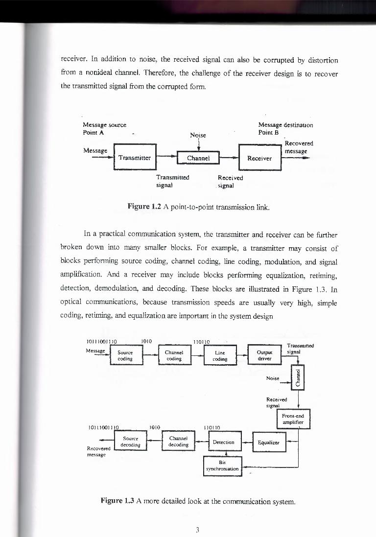
receiver. In addition to noise, the received signal can also be corrupted by distortion
from a nonideal channel. Therefore, the challenge of the receiver design is to recover
the transmitted signal from the corrupted form.
Message source Point A Noise
Message destination Point B
Me • .rr.ecove ssage I I messag
Transmitter I Channel I Receiver
red
. Transmitted signal
Received . signal
Figure 1.2 A point-to-point transmission link.
In a practical communication system, the transmitter and receiver can be further
broken down into many smaller blocks. For example, a transmitter may consist of
blocks performing source coding, channel coding, line coding, modulation, and signal
amplification. And a receiver may include blocks performing equalization, retiming,
detection, demodulation, and decoding. These blocks are illustrated in Figure 1.3. In
optical communications, because transmission speeds are usually very high, simple
coding, retiming, and equalization are important in the system design
10111001 l 10 1010 ,-.--- •• lJOl,..lO •.•• _ Transmitted Message Source
coding Channel coding
Line coding
Output driver
Noise
Received signarl ..___,
IOI l 1001110 1010 ---- ..• Front-end amplifier
110] 10
Source Recovered l decoding message I
Channel decoding Detection Equalizer
Bit synchroniation
Figure 1.3 A more detailed look at the communication system.
3

There are many different communication systems in which signals are
transmitted and detected in different ways. Differences in communication systems can
be characterized in three aspects: (1) baseband versus passband, (2) analog versus
digital, (3) coherent versus incoherent detection.
1.3 Baseband versus passband A signal can be transmitted in different frequency bands. If the signal is
transmitted over its original frequency band, the transmission is called baseband
transmission. On the other hand, if the signal is shifted to a frequency band higher than
its original baseband, it is called passband transmission. Some baseband and passband
signals are illustrated in Figure 1.4.
Signals as a function of time Corresponding spectrum
qJlJl r (a) 0
--==::,, C\ /"\. / (b) w ~v
0
VY iVii v-v (c) -le 0 Jc
(d) -Jc 0 fc
Time Frequency
Figure 1.4 Illustration of baseband and passband signals.
1.4 Analog versus digital Another important characteristic in communications is the discreteness of a
message that is transmitted. For example, if a digitized image is transmitted in discrete
4

binary bits. This is called digital communication. On the other hand, in case of AM and
FM, input signals have a continuous waveform. This is called analog communication.
1.5 Coherent versus incoherent When a transmitted signal is received, we need to detect what was originally
transmitted. If the signal is passband, it must be shifted back to the baseband. There are
two different ways to do this: coherent and incoherent detections. In coherent detection,
a different carrier source at the receiver side is used to demodulate the received signal or
to shift the passband signal back to the baseband. This carrier is generally called the
local carrier and is synchronized to the received signal in frequency and phase. On the
other hand, in incoherent detection, there is no use of the local carrier. Instead, some
nonlinear processing is used to extract the amplitude or envelope of the passband signal.
1.6 Modulation and line coding
The concept of modulation has been well known from the AM and FM. Similar
to modulation that converts a baseband signal to a passband signal, line coding converts
a binary input sequence into a suitable waveform for transmission. Because of similar
functions, line codes are also called modulation codes.
Modulation and line coding are used for different communication systems. In
general, modulation can be used in both digital and analog communications. On the
other hand, line-coding maps a finite set of signals to another set of signals with certain
properties such as de balance or frequent level transitions. Therefore, line coding is
always used in digital communication, whether baseband or passband.
1. 7 Advantages of optical communication Because of objective of communication system is to transmit messages, a
communication system is evaluated by its transmission capacity, distance, and fidelity.
Recent active research and development in optical communications has been driven by
its many advantages, such as large capacity and long distance transmission. Some
important advantages are discussed below.
1.7.1 Large transmission capacity
As mentioned earlier, when higher frequency carriers carry signals, more
information can be transmitted. For example, the capacity in microwave communication
5

IS around several hundred MHz, and it is several thousand GHz in optical
communication. As a result, transmission capacity in optical communication is not
limited by the optical channel but by the electronic speeds. This motivates the use of
parallel transmissions such as WDM.
1.7.2 Low loss Another important advantage is the low transmission loss in optical fibers.
Because of recent advancements, fiber attenuation can be as low as 0.2 dB/km at a
wavelength of 1.55 /xm. 2 In contrast, depending on the- specific carrier frequency and
the gauge of the cable, microwave waveguide loss is on the order of 1 dB/km and
twisted-pair wires is around 10 dB/km. In other words, if only loss is considered, optical
fibers can transmit signals 5 times farther than waveguides and 50 times farther than
. twisted-pair wires.
1. 7 .3 Immunity to interference
Because of the waveguide nature and easy isolation, optical signals can be
easily confined in a fiber without any external interference. In contrast, twisted-pair and
radio transmissions have significant crosstalk and multi-path interference.
1. 7.4 High-speed interconnections Optical communication is also well suited for highspeed interconnections.
Unlike electrical signals, which require a careful control of impedance matching, optical
signals can be easily transmitted and received through free space or fiber connections.
1.7.5 Parallel transmission Because optical signals can be transmitted in free space, parallel transmission in
three dimensions is possible. This provides powerful ways to interconnect large
numbers of processors for parallel processing, photonic switching, and optical
computing.
6

CHA__pTER2
OPTICAL C01\1MUNICATION DEVICES
2.1 Light Sources
In optical communication, a transmitter consists of a light source and a
modulation circuit. The light source generates an optical frequency carrier, and the
modulation circuit modulates the carrier according to the transmitted signal.
Carrier is characterized by its amplitude, frequency, and phase. An ideal carrier
can be expressed by
c(t) = A cos(wJ + ¢) (2.1)
Where its amplitude is A , circular frequency co c , and phase ¢ are time
invariant. In practice, however, a light source driven by a constant current source has the
following form:
(2.2)
Where each carrier at frequency wc,i, represents a longitudinal mode and <f>/t)
is a random phase noise. The carrier with the largest amplitude Ai is called the main
mode and the others are called side modes. A multimode source is not good for
communication.
2.1.1 Semiconductor Light Sources
Semiconductor light sources are the most important kind of light sources used in
optical communications. Their small size, low power consumption are among the
reasons for the popularity. More significantly, they can generate light signals at
wavelengths l.3µm and l.55µm, where the minimum fiber attenuation and/or dis
persion can be achieved. There are two types of semiconductor light sources: light
emitting diodes (LEDs) and laser diodes (LDs).
7
(a) P-N junction
The core of a semiconductor light source is its p-n junction, often referred to as
the active layer. The p-n junction is an interface between an N-type doped layer and a P
type doped layer. Therefore, a semiconductor light source has essentially the same p-n
junction as any semiconductor diode.
The first difference is that the material used must have a direct energy bandgap.
In a direct bandgap material such as GaAs, electrons and holes have their minimum
energies at the same momentum.
In an indirect bandgap material such as silicon, on the other hand, the energy
bands have different momenta at their minimum energies. Due to conservation of
momentum. an electron and a hole at the same momentum can directly recombine and
generate a photon.
From the above observation, the significance of direct bandgap is twofold. First,
a high direct electron and hole recombination (EHR) rate can be achieved because
electrons and holes have the highest population at their minimum energy states. Second,
because the energy release from each direct EHR is around the energy bandgap E g ,
according to the Planck-Einstein relationship, photons generated by direct EHRs are
around the same frequency
(2.3)
where h is the Planck constant. If EHRs are not direct but take place through an
intermediate interaction with the material lattice, each recombination can generate two
particles (not necessarily photons) of smaller energies M1 and M2 with
E, = M1 + M2.Be-cause M1 and M2 are undefined and random, indirect EHRs
result in an undesirable wide spectrum.
2.1.2 Light Emitting Diodes
Light-emitting diodes are semiconductor diodes that emit incoherent light when
they are biased by a forward voltage or current source. Incoherent light is an optical
carrier with a rapidly varying random phase. This random phase results from
8

independent EHRs. That is, the phase and frequency of a photon generated from an
EHR are different from those of photons from other EHRs. Therefore, incoherent light
has a broad spectrum.
The linewidth of a light source can be defined in different ways. One common
definition is called full-width half-maximum (FWHM), which is the width between two
50 percent points of the peak intensity.
~f =C
where c is speed of light, taking the total derivative, we have
For a given linewidth LU, , we thus have
(2.4)
where !if is the corresponding spectral width.
The spectrum width of LEDs depends on the material, temperature, doping level,
and light coupling structure. For AlGaAs devices, the FWHM spectrum width of LEDs
is about 2kT I h , where k is Bohzmann constant and T is temperature in Kelvin. For
InGaAsP devices, it is about 3kT I h . As the doping level increases, the linewidth also
increases.
The spectrum width also depends on the light coupling structure of the LED.
The light coupling structure couples photons out of the active layer. There are two
different light coupling structures: surface emitting and edge emitting. The first type
couples light vertically away from the layers and is called surface emitting or Burrus
LED. The second type couples light out in parallel to the layers and is called an edge
emitting LED.
Because of self-absorption along the length of the active layer, edge emitting
LEDs have smaller line widths than those of surface-emitting diodes. In addition,
because of the transverse waveguiding, the output light has an angle aroung 30° vertical
to the active layer. On the other hand, because surface-emitting LEDs have a large
coupling area, it is easier to interface them with fibers. Also they can be better cooled
because the heat sink is close to the active layer.
9

Light
Glass fiber
Epoxy resin ~----=..,
Si02
Aq stud
Metallizauon
Primary light emitting area
Figure 2.1 Illustration of a surface-emitting diode.
Current flow
Figure 2.2 Illustration of an edge-emitting diode.
10

2.1.3 Laser Principles
Another important type of light source used in optical fiber communications is
the laser diode (LD). A basic laser diode structure is similar to that of the edge-emitting
LED illustrated in Figure 2.2. By adding an additional structure for transverse photon
confinement, a coherent carrier close to what is expressed in Equation (2.1) can be
generated. Like any other lasers, the principles of semiconductor lasers are based on (a)
external pumping and (b) internal light amplification.
( a) External pumping
When a laser has several energy states, external pumping excites carriers to a
higher energy state. When they return to the ground state, they release energy and
generate photons. As an illustration, Figure 2.3 shows a simple two-level system in
which carriers (e.g., electrons) can stay at one of the two energy states E1and E2. When
there is no external pumping, most carriers stay at the ground state E1 because of
thermal stability. When there is external pumping, on the other hand, carriers at E- can
be excited to E2.
S1in1utated abxor-pt iori
F.xtema pumping
,J .
/ / ,- r:
Spontaneous S'poritane-oux t:::'tltission t:tllission
Figure 2.3 A two energy level system
(b) Light amplification
Photon generation from external pumping is not sufficient for coherent light
generation. An additional amplification mechanism is needed to multiply photons of the
same frequency and phase. In a laser, this is made possible by a quantum phenomenon
called stimulated emission. When the optical loss in a laser cavity is small from a good
11

optical confinement, a net positive amplification gain from stimulated emission can be
achieved. As a result, coherent photons can be built up.
As shown in figure 2.3, several photon emission and absorption processes exit in
a two-level atomic system. When a carrier is pumped to the upper state, it can comeback
to the ground state either spontaneously or by stimulation. The corresponding photon
generation processes are called spontaneous emission and stimulated emission,
respectively. In spontaneous emission, photons generated have random phases and
frequencies. As a result, the light is incoherent. On the other hand, photons generated
from stimulated emission have the same phase and frequency as the stimulating
photons.
Therefore, for coherent light generation, stimulated emission needs to dominate
over spontaneous emission. In addition to photon emission, figure 2.3 shows that
photons can also be absorbed to excite carriers from the ground state to upper state. This
is called stimulated absorption.
Electrons and holes in a semiconductor have emission and absorption processes
similar to those discussed above. As shown in figure 2.4, electron hole pairs (EHPs) are
generated by external current injection and stimulated photon absorption. They can later
recombine either spontaneously or by stimulated emission. Because of leaky current at
the p-n junction, there is also non-radiative carrier recombination in semiconductors.
External electron
ii" Le
Stimulated photon
absorption
Nonrudim ivc recomhinatinn
Spontaneous Stimulated 'erm ssi on ernrss ion
Extenwl hole
injection
Figure 2.4 Carrier recombination and photon emission in a semiconductor laser diode.
12

(c) Positive optical gain
In the equilibrium state, carriers have the same rate between the two states.
Thanks to Einstein, we have
(2.5)
Where S is the photon energy density, NI and N2 are carrier densities at EI and £2
respectively, BI2 is stimulated absorption rate coefficient, B2I is the stimulated
emission rate coefficient, A21 is the spontaneous emission rate coefficient, and RP is the external pumping rate in a unit volume. Therefore, the left-hand side of equation (2.5) is
the total rate from E2 to E1, and the right-hand side is the total rate from EI to E2 •
From equation (2.5), when there is no external pumping (RP = 0), the photon energy
density S in equilibrium is
Uoule I m' .Hz j (2.6)
where the last equality comes from the Planck-Boltzmann's black-body radiation
distribution. Equation (2.6) implies BI2 = B21 and (A21 / B2i) = (srchf3 n3 / c3 ), where n
is the refractive index of the medium.
To increase the stimulated emission rate, the light intensity S must be increased.
In general, the light intensity increases at a rate proportional to ( B21 N 2 - B12 N1) S ,
which is the photon stimulated emission rate minus the photon stimulated absorption
rate. Building up the light intensity thus requires that
(2.7)
This condition is commonly referred to as population inversion and requires that
To achieve population inversion, the external pumping rate (RP) needs to be greater than the spontaneous emission rate. This can be seen by rearranging equation
(2.5) as
S= Rp-A21N2
B21N2 - B12N1 (2.8)
13

Because S > 0, RP needs to be higher than the spontaneous emission rate (A21Ni)
when
2.1.4 Fabry-Perot Laser Diodes
A basic LD that has a rectangular cavity is equivalent to a Fabry-Perot
(FP) resonator. An LD that has a simple rectangular cavity is thus called an FP LD.
(a) Power loss and gain
When photons are reflected back and forth between the two FP cavity ends, they
experience both gain and loss. The gain comes from stimulated emission, and the loss
comes from medium absorption and partial reflections at the two cavity ends. In the
steady state, the gain and loss are equal. From this condition, the required gain from stimulated emission can be derived.
A round
z = L Vertical direction
z = ()
Figure 2.5 Illustration of a laser cavity
14

For simple discussion, assume the wave function of a light wave is a scalar and
has a value A (a complex variable) at point z=O. From Figure 2.5, the wave traveling to
the right can be expressed as
E+ (z) = A/Jf3,-a12+g12)z
where f3 z is the propagation constant along the z-axis, and a and g are the
distributed medium loss and gain, respectively. The time dependence factor e jwt of the
field is dropped for its irrelevance, and the power of the traveling wave is proportional
to e(g-a)z. At z = L, the wave function has value A/J/3,-a+g)L Assuming the cavity end
on the right has a reflection coefficient of r2, the reflected wave traveling to the left can
be written as:
The round trip is complete after the left-traveling wave is reflected back by the
left mirror with reflection coefficient r1• Therefore, the conditions of a unit round trip
gain in the steady state are
r r e(g-a)L l 2 = 1 (2.9)
and
2L/32 = 2mn (2.10)
where mis an integer. Equation (2.9) can be expressed as
(2.11)
where am accounts for the reflection loss at the cavity ends. Equation (2.11) is
the gain-loss condition at the steady state, and equation (2.10) is the phase condition for
the laser wavelength. This second condition is the basis for the longitudinal modes.
The gain-loss condition in equation (2.11) is only applicable to the steady state.
Before the laser reaches its steady state, the gain is greater than the total loss. This
builds up the radiation field in the laser by stimulating more photons from carrier
recombination. As the laser field is being built up, there are more stimulated emissions
or EHRs. This brings down the carrier density and also the gain. Finally a steady state is
reached where the stimulated emission rate is in equilibrium with the carrier supply or
generation rate. Therefore, the output power is determined by the injected current
supply.
(b) Longitudinal modes
Substituting f3z = Znn] A into the roundtrip phase condition given by equation (2.10), we have
)., _ 2Ln m - -
m (2.12)
where n is the refractive index of the gain medium and Am is the m th
longitudinal mode. Where m is the large integer, the longitudinal mode separation
between Am and Am+i is
, { 1 l } 1 A2 ~ =A -A =2Ln ---- ;::;;2Ln-=-- long m m+l l ? 2L m m+ m: n (2.13)
When an externally injected current generates carriers, depending on their
energy distributions in the conduction and valence bands, they contribute to stimulated
emission at different longitudinal modes.
2.1.5 Single Mode Laser Diodes
FP laser diodes generate undesirable multiple longitudinal modes. A different
kind of laser diode called the single mode laser can suppress side modes and generate
only one main longitudinal mode. Important single mode lasers include: DFB
(distributed feed-back) lasers, DBR (distributed Bragg reflector) lasers, and cleaved
coupled-cavity ( C 3) lasers.
(a) DFB lasers
DFB lasers use Bragg reflection to suppress undesirable modes. As illustrated in
figure 2.6, there is a periodic structure inside the cavity with the period equal to A.
Because of the periodic structure, a forward traveling wave has interference with a
16

backward traveling wave. To have constructive interference, the roundtrip phase change
over one period should be 2mn, where mis an integer and is called the order of the
Bragg diffraction. With m = 1 , the first order Bragg wavelength is
or
AB= 2J\n (2.14)
p-lnGaAsP
N-lnP substrate
..,.__ Transverse direction
Figure 2.6 Illustration of a buried-hetrostructure DFB LD
Therefore, the period of the periodic structure determines the wavelength of the
single-mode light output. In reality, a periodic DFB structure generates two main modes
with symmetric offsets from the Bragg wavelength; a phase-shift of A I 4 can be used to remove the symmetry. As illustrated in figure 2. 7, the periodic structure has a phase
discontinuity of re I 2 at the middle, which gives an equivalent A I 4 phase shift.
(b) DER lasers
DBR lasers use the same Bragg reflection principle to generate only one
longitudinal mode. The difference between DBR and DFB lasers is that DBR lasers
have the diffraction structure outside the laser cavity, as shown in figure 2.8. With this
arrangement, the laser control and the frequency control can be done separately.
17

(c) Coupled cavity lasers
A coupled-cavity laser has two FP resonant cavities, which can be both active or
one active and one passive. These lasers are illustrated in figure 2.9. In either case, the
basic principle to generate only a single longitudinal mode is illustrated in figure 2 .10.
1 _ 2L1n _ 2L2n II,------
(2.15)
:\1..:ti\ i..: I~ 1 \ t.' r
Figure 2. 7 Illustration of a A I 4 phase-shift D FB LD.
Where m1 and m2 are two integers. With A satisfying equation (2.15) and using
equation (2.13 ), the modal separation is
(2.16)
Where M 1 and M 2 are two mutually prime integers such that
L L def 1 _ 2 _ L
---- 0
M1 M2 (2.17)
).,2
M1ong = 2nLo (2.18)
18

Lnn~ill1di11;1J 1iit"L'L·1i11n ------------~
Figure 2.8 Illustration of a DBR LD.
Laser Modulator
All four facets cleared and parallel
Not to scale
(a)
Light output Anti-reflection coating
Capillary tube
Laser sw.d
(b)
Figure 2.9 Illustration of coupled-cavity LDs ( a) active-active, (b) active-passive
19

111111 l Longitudinal modes of cavity l
~ Wavelength
(al
1 1 l 1 l Longitudinal modes of 1..:a,·lt; 2 ..
Wavelength
(b)
~ Mi1111nu111 gain ..
\V avelength
(C)
Figure 2.10 Principle of coupled-cavity diodes
2.2 Optical Fibers Our current "age of technology" is the result of many brilliant inventions and
discoveries, but it is our ability to transmit information and the media we use to do it,
that is perhaps most responsible for its evolution. Progressing copper wire of a century
ago to today's fiber optic cable, our increasing ability to transmit more information,
more quickly and over longer distances has expanded the boundaries of our
technological development in all areas.
Signal Input S ig,n.al Oulp1Jt
F,be,r Oplic Cabla OPTICAL
TRANS MITT ER ! .t
Figure 2.11 Illustration of Optical Fiber Communication
20

Today's low-loss glass fiber optic cable offers almost unlimited bandwidth and
unique advantages over previously developed transmission media. The basic point-to
point fiber optic transmission system consists of three basic elements: the optical
transmitter, the fiber optic cable and the optical receiver (figure 2.11).
Fibers are a common transmission medium used in optical communications.
Compared with other transmission media such as space and wires, optical fibers provide
low attenuation and strong immunity to electromagnetic interference (EMI). Because of
these advantages, optical fibers have been used in long-haul undersea and interoffice
communications Optical fibers are the communication channel in which light
propagates. Like any other transmission medium, signal attenuation and distortion in
optical fibers are important degradation factors.
2.2.1 Structure and Types
A bas c opt cal f ber has a c rcular cross sect on as dep cted n Figure 2.12
Although a practical fiber has many layers, only the core and cladding are important to
light propagations. Both the core and cladding are typically made of silica glass,
however, the core has a higher refractive index to confine light inside.
As light propagates inside a fiber, most of its power is confined in the core
region, which is surrounded by the cladding. The cladding has a slightly lower optical
density ( or refraction index), typically between a fraction of 1 percent and a few
percent. Most fibers have the cladding diameter around 125 µ m. Its size is generally not
important to light propagations. Outside the cladding are several layers of protection
jackets. The jackets prevent the fiber surface from being scratched or cut by mechanical
forces.
Cladding
-100µ.m
(a) (b)
Figure 2.12 Basic structures of (a)_Single mode (b) Multiple mode optical fibers.
21

(a) Single mode and multimode fibers
When a lightwave propagates inside the core of a fiber, it can have different EM
field distributions over the fiber cross-section. Each field distribution that meets the
Maxwell equations and the boundary condition at the core-cladding interface is called a
transverse mode.
Several transverse modes are illustrated in Figure 2.13. As shown, they have
different electric field distribution over the fiber cross-section. In general, different
transverse modes propagate along the fiber at different speeds. Fibers that allow
propagation of only one transverse mode are called single-mode fibers (SMF). Fibers
that allow propagation of multiple transverse modes are called multimode fibers (MMF).
The key in fiber design to having single-mode propagation is to have a small
core diameter. This can be understood from the dependence of the cutoff wavelength Ac
of the fiber on the core diameter. The cutoff wavelength is the wavelength above, which
there can be only one single transverse mode. Ac is expressed as
_ Zna ( 2 _ 2)112 ), --- n1 n: C V - (2.19)
Where V=2.405 for step-index fibers. A is the core radius, n1 and n2 are the
refractive indices of the core and cladding, respectively. This expression shows that
fibers of a smaller core radius have a smaller cutoff wavelength.
22

I.Poi HEi1
T'Eo1
LP11 ™o,
HE~1
LP21 {
EH11
HE31
(B) (b)
0 0 + ;
0 @ 0 ©
(c) (d)
Figure 2.13 Some examples oflow-order transverse modes of step-index fiber, (a)
Linear polarized (LP) mode designations, (b) Exact mode designations, ( c) Electric field
distribution, ( d) Intensity distribution of electric field component Ex
When the core diameter of a single-mode fiber is not much larger than the
wavelength, there is a significant power portion or field penetration in the cladding.
Therefore, it is necessary to define another parameter called mode field diameter
(MFD). Intuitively, it is the "width" of the transverse field. Specifically, it is the root
mean square (RMS) width of the field if the field distribution is Gaussian.
2.2.2 Light Propagation in Fiber Optics
In addition to attenuation, fiber dispersion is another limiting factor in lightwave
transmission. Dispersion is a phenomenon that photons of different frequencies or
modes propagate at different speeds. As a result, a light pulse gets broader as it
propagates along the fiber. This section first explains the basic physics of light
propagation in optical fibers.
Signal propagation in optical fibers can be described by either geometrical optics
or Maxwell's equations. Geometrical optics is a good approximation when the
wavelength of light is relatively small compared-to the system's dimensions. On the
23

other hand, solving Maxwell's equations can tell the exact story but is much more
mathematically complex. This section uses both methods to study light propagation, but
avoids complex mathematics such as solving wave equations in optical fibers. Instead, it
stresses the relationship between geometrical optics and wave functions. This approach
shows the insight of the physics of lightwave propagation with minimal mathematics.
(a) Signal propagation by geometrical optics
The geometrical optics model for fiber propagation is illustrated in Figure 2.14,
where incident light from a light source emits "rays" to a fiber in different directions.
From Snell's refraction law, each ray will go partially into the cladding region or be
totally reflected back depending on its incident angle 81 at the core-cladding boundary.
CJ adding n2
Figure 2.14 Light propagation using geometrical optics.
More spec f cally, a ray will go partially into the cladding if a 8 2 exists such that
(2.20)
Where n1 and n2 are the refractive indices of the core and cladding respectively.
Because n1 > n2 , a complete internal reflection is possible if
[n Jdef e I > Sin -1 < = e crit . (2.21)
24

That is, the corresponding ray will be totally reflected back to the core. As a
result, a ray will propagate along the fiber without loss ( other than various attenuation
sources discussed earlier) if the incident angle e1 satisfies Equation (2.21 ).
Figure 2.15 provides two further, important observations first, rays with
different 81 > e crit have different z -component velocities. Specifically, for a ray of e1
its z component velocity is
(2.22)
This velocity dependence on e 1 results in different propagation delays or
dispersion. To reduce dispersion, graded-index fibers mentioned earlier can be used.
Ray propagation in a graded-index fiber is illustrated in Figure 2.15. As shown,
although rays of larger e 1 propagate in a shorter distance, they travel through a higher refractive index region. On the other hand, rays of smaller e I travel a longer distance but through a lower refractive index region. As a result, graded-index fibers can
equalize the propagation delay of different propagation rays, and greatly reduce the fiber
dispersion.
Another important observation is that rays at larger e1 's have larger z
component velocities, and consequently smaller radial velocities. Intuitively, we see that
the larger the radial velocity, the higher the penetration of the light power into the
cladding region. As the wave analysis will demonstrate shortly, rays of larger radial
velocities correspond to higher propagation modes. When the radial velocity becomes
too large or e 1 > e crit , the ray will propagate into the cladding and never come back.
Index profile
Figure 2.15 Ray propagation in the graded-index fiber.
25

The critical angle condition of equation (2.21) from geometrical optics gives the
condition of propagatable rays. When e crit is large or n2 is very close to n1, the incident
ray has to be closely parallel to the fiber axis. Therefore, it is more difficult to inject
light into the fiber for propagation. To quantify the ease of coupling light into a fiber for
propagation, a parameter called numerical aperture (NA) defined by
def .---- NA= 1n2 -n2 "tJ I 2 (2.23)
has been used. Because n1 is close to n2 in optical fibers,
n:-n; =(n1 +n2)(n1 -n2)~2n;[(n1 -n2)/n2]. NA in equation (2.23) can thus be
approximated by
(2.24)
is the ratio of the refractive index difference.
The physical meaning of NA can be seen as follows. An incident ray that can
propagate in the fiber should be within the solid angle given by
r. cone area 2 [l (B. )] 4 ir 2(B,n) . 2(e. ) 1..: = - = 7r: - COS = n Slll - ~ n Slil d? ,n 2 ,n (2.25)
when B,n << 1. From figure 2.17 and equation (2.21),
sin( e in)= n. cos(e crit) = nl [1- sin 2 (8 crit) J12 = Gt - n; t2 = NA (2.26)
Therefore,
" Q ~ n (n: - n;) = nNA 2 (2.27)
This shows that larger the NA, the larger the solid angle within which incident
light can propagate.
(b) Fiber dispersion
If an optical pulse consists of components at different frequencies and different
propagation modes, different propagation delays from these components will result in a
broader pulse at the other end of the fiber. This phenomenon is known as Fiber
Dispersion.
26

2.3 Light Detection
Light detection is a process that converts incident light into an electrical
photocurrent. Alight detection device is used at the front end of every optical receiver to
generate a photocurrent proportional to the incident light.
There are two main types of light detection devices: photoconductors and
photodiodes. They are both semiconductor devices.
2.3.1 Photoconductors
There are two main types of photoconductors: intrinsic and extrinsic. An
intrinsic photoconductor is an intrinsic semiconductor. Its conductivity increases when
electrons are excited from the valence band to the conduction band. When there is
incident light onto the photoconductor, electrons and holes are excited. As a result, the
conductivity increases. On the other hand, an extrinsic photoconductor is a
semiconductor with either N-type or P-type doping. Its conductivity increases when
electrons (or holes) are excited from there N-type (or P-type) impurity levels. Because
extrinsic photoconductors have free carriers, they have low resistance. This is
undesirable from the thermal noise consideration. Therefore, the conductance of a
photoconductor should be made as small as possible. From this consideration intrinsic
photoconductors are better than extrinsic ones.
The current gain and frequency response of an intrinsic photoconductor are
derived as follows. At an incident light power of f>;n the amount of the carrier density
increase ( electrons and holes) is •
(2.28)
Where re is the relaxation time of the photoconductor and V is the volume of
the absorption layer. If the photoconductor is in series with a bias resistance RF as
shown in Figure 2.16, the amount of increased current is
Ai_ VDD VDD R;VDD [qr, ( )r 1 ] - RF +Rc -t:,Rc - RF +Re~ (Rc +RF)2 hf f>;n µn + µp e d2 (2.29)
where µn and µ P are the mobilities of electrons and holes, respectively.
27

Ptmiocondm::tor
R,.
Figure 2.16 Circuit connection of a photoconductor for light detection.
2.3.2 Photodiodes
There are two types of photodiodes: PINs and APDs. A photon with sufficient
energy can excite an electron-hole pair. If the pair is in the presence of a large electric
field, the electron and hole will be separated and move quickly in opposite directions,
resulting in a photocurrent.
Because one absorbed photon generates one EHP in PINs, the p~otocurrent is a
linear function of the input optical power P,n :
I ph = Yf !LP,,., = ( f/A )p hf 1.24 m
(2.30)
where r, is quantum efficiency.
For APDs, because of the current gain from EHP multiplications, the generated photocurrent is
I - M ( YfA )p ph - apd l .24 in (2.31)
28

CHAPTER3
SIGNAL PROCESSING
To provide high bit rate and long distance transmission, there have been many
significant breakthroughs. For example, to overcome power loss due to fiber
attenuation, optical amplifiers have been developed and installed in practical systems; to
increase receiver sensitivity, coherent communication and external modulation have
been used; and to overcome fiber dispersion, single frequency light sources and soliton
transmission have been developed.
3.1 Direct Modulation The light output must be modulated in either amplitude, frequency, or phase to
transmit information. As illustrated in Figure 3 .1, according to position where
modulation is performed, light modulation can be classified as either direct or external
modulation. With direct modulation, light is directly modulated inside a light a source.
External modulation, on the other hand, uses a separate, external modulator. ••
Bias current Light
source Modulated output
••
Modulating input signal
(a)
Bias cw current Light carrier External Modulated outp
source modulator UI
1 Moduluting input signal
(b)
Figure 3.1 (a) Direct modulation (b) external modulation.
Direct modulation is used in most optical communication systems for its simpler
implementation than external modulation. Because of physical limitations, the light
output under direct modulation cannot respond to the input signal instantaneously.
29

Instead, there can be delays and oscillations when the input has large and rapid
variations. Finding the light output under direct modulation requires using rate
equations, which describe the dynamics of photons and carriers inside the active layer of
the light source. The light output and the modulation bandwidth under certain bias
condition can be determined from the rate equations.
Direct modulation has several undesirable effects such as frequency chirping and
line width broadening. In frequency chirping, the spectrum of the light output is time
varying because of refractive index modulation of the light source, and in line width
broadening, the spectrum width is broader than that in the steady state. These effects can
be the limiting factors in long distance and high-speed communications. To reduce these
effects, external modulation can be used. In this case, the bias current to the light source
is constant, and a separate modulator is used to modulate the continuous wave (CW)
output of the light source.
•
3.1.1 Direct Modulation for LEDs
Direct modulation uses the input current to modulate the output light intensity.
Because the light output of an LED is incoherent, the phase or frequency content of the
output is not of interest. Therefore, the following analysis considers only the intensity or
power of the modulated light.
(a) Rate equation for laser diodes and steady state solution
Whether in steady state or under modulation, the light intensity output of an
LED can be derived from a single rate equation that describes the dynamic relationship
between the carrier density and the input current. If the active layer of an LED is N-type
of donor concentration ND , the rate equation is
dN J dt :::: qd -B(NP-n:)- N-ND
r nr (3.1)
Where N is the electron density, P is the hole density, J is the current density, d
is the thickness of the active layer, r nr in the nonradiative time decay constant for the
electrons, and Bis the electron- hole recombination coefficient.
The above rate equation (3 .1) can be understood from charge conservation. On
the left hand, dN I dt is the net charge rate of the electron density of the p-n junction.
On the right hand side are various sources for the rate change. The first term is the
30

carrier-pumping rate due to external current density. The second term is the net radiative.
electron-hole recombination (EHR) rate. Finally the third term is the net nonradiative
carrier recombination rate inside the active layer.
Because it is the EHR of the second term on the right hand side of equation (3.1)
that contributes to the spontaneous emission, the optical power output is
P(t) = TJex1hfVB(NP- n;) (3.2)
Where T] exr is the external quantum efficiency that represents the fraction of
photons coupled to the output, hf is the photon energy and V is the active layer
volume.
In the steady state, dN I dt =O. There fore,
_!_=B(NP-n;)+ (N-ND) qd TM
According to charge neutrality,
n2 NP-n2 = N(N -N +-i )-n2;::; N2 -N N'
I D N I D~ D
(3.3)
• It is convenient to define
def 1 r ; = BN (3.4)
Where r,.,. is called the radiative recombination time constant. It depends on the carrier
density. 1
1 def 1 _l_ = BN + --- - = -- - + (3.5) f T f Tr f nr f nr
The rate equation in the steady reduces to
J N-ND (3.6) =
qd r r
From equation (3.3),
B(NP-n;2)= N-ND =!.c__!_ r rr r rr qd
(3.7)
The ratio
1/-r def = . rr r l' =TJ· rr i r rr + l!-r int nr
(3.8)
31
rs called the internal quantum efficiency, meaning the ratio of the radiative
recombination rate to the total recombination rate. From equations (3 .2), (3. 7), and
(3.8), the optical power output can be related to the input current by
J hf 1.24 P = 11exrhfVB(NP - n;2) = 11ext11inthjV- = 17-J = 17 I qd q J,.,(µm) (3.9)
Where
17 = 17 ext 17 int is the total quantum efficiency.
(b) Digital signal modulation
On-off keying (OOK) is a common signaling scheme in digital communications.
In this scheme a pulse is send to convey a bit "1" and nothing is sent to transmit bit "O" for one bit interval.
Output light power, mW
3.50 CTurn-onL 3.00 ~_e_l_ax .....
2.50 i
2.00 r
... 90'1<: l"'ak 3.39 mW
A = 5e-8 sec-! 1 -1 B = 8e- I I cmsec
N0= lel8cm-3 I= 50 mA d= le-5cm L = le-2 cm »· = le-4 cm
77 "' = O.l
h .,
I.SO
1.00
0.50
0.00 0.00 2.00 4.00 6.00
Time (nsec)
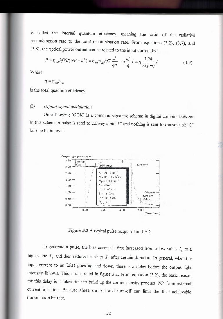
Figure 3.2 A typical pulse output of an LED.
To generate a pulse, the bias current is first increased from a low value JI to a
high value 12 and then reduced back to JI after certain duration. In general, when the
input current to an LED goes up and down, there is a delay before the output light
intensity follows. This is illustrated in figure 3 .2. From equation (3 .2), the basic reason
for this delay is it takes time to build up the carrier density product NP from external
current injection. Because these tum-on and tum-off can limit the final achievable transmission bit rate.
32

To derive these delays we have to solve the rate equation (3.1) for a step two
input: one goes from low to high, and one goes from high to low. Consider the first
case, in which a step input goes from low 11 to high 12• The initial condition at time
zero for 1 is
I 7\f -N ] 1(0)=11 =qdj B(N1P.,-n;2)+ · 1-r D
L • nr
Where def
NPI = N.P. lt=O i '
Similarly, the steady state condition for J = J 2 at t = oo
Where
From charge neutrality, the number of electrons and holes generated are always the
same. It is thus possible to define def
Ml(t) = N(t)-N1 = P(t)-P., (3.10)
As the carrier density increases from the initial value at t = 0. From equations (3.1) and
(3.10), fort> 0,
d[1N(t)] = !.i_ _ B(Nl + ,0,lv)(P., + &7\f) + Bn;2 - -1 (&7\f + NI - ND) dt qd Tnr (3.11)
Where 1 def 1 - = B(N1 +P., +M/)+-
r step T nr
(3.12)
(c) Analog signal modulation
In analog communications, the information signal is added to a DC bias to form
the total current input to a light source. From the nonlinear rate equation at a large
current the signal component needs to be small compared to the DC bias to maintain
33

high end-to-end waveform linearity. Therefore, analog communication can be
considered as small signal modulation.
Previously we have analyzed turn-on and turn-off delays with pulse modulation.
In analog communications, on the other hand, the modulation bandwidth for the small
signal input is of interest. The time-frequency duality suggests that the delay and
bandwidth analysis yield LED in pulse modulation, the larger the 3 dB bandwidth in
small signal modulation.
To proceed, consider a single tone input frequency co :
J(t) = 10[1 + km cos(cot)] (3.13)
Where JO is the bias current density and s; is the amplitude modulation index. Let N1
be the carrier density at JO , and let
def
N(t) = N1 + Ml cos(cot-<j)) (3.14)
Where the second term is small signal term due to the single tone input. From the above
two equations, the rate equation (3.1) reduces to
-AN co sin((J)t-<f>) = ~k111 cos(cot )--1 Ml cos(cot -¢) qd rac
(3.15)
Where
J def } -=B(Ni +JD+- r ac rnr
(3.16)
The solution to equation (3.15) is
Al\T=~k } LlJV T , , d m ac ( 2 2 y12 q I+co rac/ (3.17)
And
~ = cos-{ ( ,1 , )"' J \ 1 + co r ac
(3.18)
From equation (3.17), the output power is
(3.19)
Therefore, the signal part is
I 1 M(t) =r,hf-0 k"' ( viz cos(cot-</>)
q 1 +w2r:c (3.20)
34
From equation (3.20), the 3 dB optical signal bandwidth is
B = ,J3 = 0.28 opt,3dB 2 'TCT T ac ac
(3.21)
Based on the final photocurrent signal on the receiver side, the 3 dB electrical signal bandwidth is
I 0.16 Belec,3dB = l'TCT Tac
- ac (3.22)
The results show that the 3 dB frequency response is determined solely by the time
constant r . ac
3.1.2 Rate Equation for Laser Diodes
Similar to LEDs, laser diodes can be directly modulated by varying the bias
current. Because carriers interact with photons in the laser generation process, there are
separate rate equations to describe the dynamics of carriers and photons. These
equations can quantify and explain various important phenomena such as tum-on delay,
relaxation oscillation, chirping, and linewidth broadening.
(a) Laser rate equation for carrier density
Based on the laser generation dynamics, the rate equation for the carrier density
can be written. Similar to the rate equation of LEDs, it can be expressed as
8N J(t) _ R( 11.T N ) = J(t) _ N - Fv g(lv)lv h at = q d l V ' ph q d r .( N) g p (3.23)
Where R ( N, N ph) is the total carrier recombination rate and is a function of the carrier
density N and photon density N ph " Specifically, for a lightly doped active layer,
R ( N, N ph ) can be expressed as
R(N,Nph) =AN+ BN2 + CN3 + ['vgg(N)Nph N -- + rv g(N)lv h rJN) g p
(3.24)
Where
• AN = NI r is the nonradiative recombination rate. nr
• BN2 is the radiative spontaneous emission rate.
35

• CN3 is called the Auger recombination rate. def
• 1 Ire ( N) ::::: A + BN + CN2 is the effective recombination rate.
• rvgg(N)Nph is the stimulated emission rate.
In the stimulated emission term given above, vg is the group velocity, r is the cavity confinement factor, and
g(N) = a(N -N0) (3.25)
is the optical gain, with a being the gain constant.
To include the gain suppression effect, the gain constant can be expressed as
(3.26)
Where the parameter T/ g is called the gain suppression coefficient. The gain constant a
decreases as the optical intensity increases.
(b) Rate equation for photon density
Similar to the carrier density rate equation, the photon density rate equation can
be formulated according to the sources of its rate change. Because the photon density in
a cavity is determined by the stimulated emission rate, spontaneous emission rate, and
cavity loss, the following rate equation holds:
dN h N h _P_ = Tv g(1V)1V - _P + {3 BN2 dt g ph T sp ph
(3.27)
Where the parameter {3 sp represents the percentage of the spontaneous emission that
happens to be coherent with and in phase to that of the stimulated emission, and r ph is
the photon decay constant related to the total cavity loss a101•
The photon decay constant r ph can be expressed in terms of the total cavity loss
a101• Because the photon decay over one trip in the cavity has a factor of e-a.w,L and
takes a time of Llvg,
-Livg'ph -a101L e =e
36

Therefore,
(3.28)
3.1.3 PuJse Input Response for Laser Diodes
The rate equations given earlier can be used to study the pulse input response of
laser diodes for digital transmission. A typical pulse input response from numerically
solving equations (3.23) and (3.27) is shown in figure 3.3. Clearly laser diodes respond
quite differently from LEDs. On the rising edge, a turn-on delay is followed by an
oscillation. On the falling edge, there is a sharp drop or negligible turn-off delay.
" "' g_ 4.00 "' ~ C: .s ;;; 3.00 :i ti e ~ 2.00 = 0.. ti
" ,..., 'a 1.00 E 5 z
5.00
0.00
I I I I I I
' Photon :: density :: response :: · -: : i Relaxation oscillation
,,,~ ,, I ,, I 11 1,
Carrier : : :: :: . 1• ,, 11
densitv 1 1 11 11 ; ~ t I l t I I Jt
~·::•:::: .. ,,. I I I ! I I I ! I! I\ , ' I I '\ ~ p ( \ , / ,
- : : : : : : : ·~ : '1 : \ .1 ' ,' I, ' , • '
J I J I ! ' ! ,1 ~ I It 11 \J I II,,!
Sharp ~ falling -i '-.. edge 1 I _
1, = 0.21,h J, = 1.21,h
8.00 J0.00 4.00 6.00 2.00
Initial delay t d Tirne tnsec)
Figure 3.3 Pulse modulation response.
The behavior illustrated in figure 3.3 can be qualitatively understood as follows.
First, careful examination of equation (3 .27) shows that the rate of increase dN ph I dt is
essentially zero when N ph is small. It will not become significantly positive until the
net gain is positive:
1 f'vgg(N)-->0
r ph
37

Therefore, when the laser diode is turned on, the photon density due to
stimulated emission will stay essentially zero until N reaches its threshold N1h. This
can be clearly seen from figure 3.3, where the normalized carrier density NI N1h is
shown. The delay for the carrier density to reach N1h is called the turn-on delay.
3.1.4 Small Signal Response for Laser Diodes
Similar to LEDs, small signal analysis of laser diodes is useful for analog
communications. A similar analysis can help explain the modulation bandwidth of a
single tone current input.
For convenience, a single tone current input at the circular frequency w,,, is
expressed by
J(t) = Jo ll + «; exp(Jwmt) J (3.29) .
Where k . is the modulation index for the input current and J0 is the bias current m,J
density. Similarly the following forms can be assumed for the carrier and photons
densities:
N(t) = Nn,O ll + s., exp(jwmt) J (3.30)
And
(3.31)
Where k,,,,n and km,ph are modulation indices of the modulated carrier and photon
densities, respectively. In general, they can be complex to represent possible phase
shifts with respect to J(t).
3.2 External Modulation
To avoid undesirable chirping and mode partitioning in direct modulation,
external modulation is a good alternative. A basic external modulator is general consists
of an optical waveguide in which the incident light passes through and the refractive
index of the medium is modulated by the information bearing signal. According to the
way the refractive index is modulated, there are two primary types of modulation:
electro-optic (EO) and acousto-optic (AO), where the refractive index is modulated by
either a voltage input or an acousto wave, respectively.
38

3.2.1 Principles of External Modulation As described earlier, there are two primary types of external modulators: EO and
AO modulators. In EO modulators, a constant refractive index change is introduced by
an external voltage signal. In AO modulators, a periodic change of the refractive index
in introduced by an acoustic wave.
(a) Electro-optic modulator
An EO modulator can be as simple as an optical channel or waveguide through
which incident light passes. For many media used in EO modulators, the incident light
"sees" different refractive indices at different polarizations.
Let /3 0 and /3 b be two propagation constants, both of which can be modulated
by an external voltage signal. The electric field at the waveguide output can be written
as A A
Es: = Aae-JflaL Sa+ Abe-Jfl,L Sb (3.32)
(b) Acousto-optic modulator In AO modulators, the periodic modulation of the refractive index forms a
grating. As a result, the incident light is diffracted. Thus the grating can be controlled to
modulate either the through light or the diffracted light. In general, the grating structure created in AO modulation is similar to the
periodic Bragg reflector structure of DFB lasers. As a result, there are two waves inside
the modulator, one in the same direction as the incident wave and the other diffracted by
the grating. These two waves interact as they propagate along the modulator and are
similarly governed by the coupled mode equations. As a result, by modulating the
coupling constant through the input acoustic wave, the light out put can be modulated.
3.2.2 Wave Propagation in Anisotropic Media A medium that responds differently to the different polarizations of incident
light is called anisotropic. A medium that has the same response to different
polarizations is called isotropic. When the medium of an external modulator is
modulated, it can tum from isotropic to anisotropic. In fact, to achieve large modulation
depth and power efficiency, an external modulator should have a large response to
either the EO or AO effect.
39

(a) Anisotropic materials
The response of a medium to incident light is characterized by its permittivity.
For an anisotropic medium, its response depends on the polarization of the light. As a
result, its permittivity is no longer a constant. Instead, it is a tensor or a three by three - -
matrix through which the electric flux density D is related to the electric field E by
D_ I e~ & e; l .ry
D=ID = s syy e,, j~eE (3.33) y JI."
Dz &zx &zy e:
* From basic physics, it can be verified that &iJ = 8 Ji. Therefore, it can be
transformed to a diagonal matrix.
(3.34)
The axes that result in the above equation are called principle axes.
(b) Normal surfaces
To find the two permissible plane waves propagating in a given direction
requires using Fresnel equation (3.35) to solve the propagation constants and using
equation (3.36) to find the polarizations. These results, allow one to find the
birefringence and design the external modulator.
s2 s2 s2 1 _ __:x:___ + Y + z = _ 112 - 112 112 - 112 n' - 112 n'
1 2 3
(3.35)
(3.36)
(3.37)
40

The first method is the use of the so-called normal surface, which is defined as
the set of all points (nsx,nsy,nsJ with n satisfying equation (3.35). Therefore, for a
given propagation direction s, n0 and nb can be found by generating a ray in the same
direction s from the origin. The distance of the intersection of the ray with the normal
surface gives the corresponding n value.
n Optic axis n;
X .r X
(a) (b) (c)
Figure 3.4 Normal surfaces (a) isotropic (b) uniax.ial (c) biaxial crystal.
The normal surface can be constructed as follows. For the special case that
s, = 0 or f3 is in the x-y plane, equation (3.37) reduces to n' = n: 3 (3.38)
And
1 2 s2 s X y -=-+ n2 n: n'
2 1
(3.39)
Equations (3.38) and (3.39) allow the two curves to be drawn on the x-y plane as
illustrated in figure 3.4. Note that in figures 3.4b and 3.4c, there is a special axis called
the optic axis, which is defined to be the propagation direction in which the two n values are the same.
3.2.3 Electro-Optic Modulation
This kind of modulation deals with the basic principles ofEO modulation.
41

(a) Modulation of refractive indices
When an external voltage is applied to an EO crystal, the electric field present in
the crystal can modulate its refractive index tensor. The electro-optic effect can be
characterized by the change of the impermeability tensor:
(3.40)
The linear coefficients rWl* are called the Pockels coefficients, and the quadratic
coefficients sC/JJCkll are called the Kerr coefficients. In general, the Kerr effect is
insignificant unless the Pockels coefficients are all zero. Crystals that have zero Pockels
effect have a centrosymmetric crystal structure. For most optical EO modulators that are
not centrosymmetric, only the linear Pockels effect must be considered.
Given the change of the impermeability from the external electric field, the
index ellipsoid equation can be expressed as
(3.41) 1
+ 2~17nyz + 2~1J31ZX + 2~1J12xy = -2 n In general, from the symmetry of ~11u = ~T]Ji, the new index ellipsoid can be
transformed into the canonical form given by following equation
x2 y2 z' 1 -+-+-= n2 n2 n2 n2
l 2 3
(3.42)
This means that the principle axis of the crystal can rotate in the presence of an external
field.
(b) Longitudinal and transverse modulators
According to the relative direction of the bias electric field and the light wave
propagation, an EO modulator can be classified into two categories: transversal and
longitudinal. As illustrated in figure 3.5, the bias electric field is perpendicular to the
wave propagation direction in transverse modulation; and in longitudinal modulation,
the bias electric field is in the same direction as the wave propagation.
42

(a) (b)
Figure 3.5 (a) Transverse (b) Longitudinal modulators.
For a given birefringence B, the two polarizations over a propagation distance L will have a phase difference ~</> given by
~</> = (/30 - f3JL = (n0 - nJco L = co BL C C
For longitudinal modulators, from equation (3.43) the phase change of a given
(3.43)
permissible polarization is linearly proportional to the applied electric field Ez.
Therefore, if the lightwave propagates in the z direction,
(3.44)
Where Ve is the external bias voltage and r is the EO coefficient according to the wave
polarization.
3.2.4 Acousto-Optic Modulation
Similar to EO modulation, AO modulation uses sound waves to modulate the
refractive index of the medium. The difference is that sound waves have periodic
compression and refraction patterns that result in periodic variations of the medium's
refractive index. This periodic variation of the refractive index acts as a phase grating
that diffracts part or all of the incident light.
(a) Electro-optic coefficients
Similar to electro-optic coefficients, there are a so-called elasto-optic coefficient
that quantifies the change of the permeability tensor under an acoustic wave.
For an acoustic wave U(O.t - K.r) in a medium with propagation constant K,
the strain tensor is defined as
43

au, s(ij) = a-r
J
(3.45)
Because the acoustic wave U is in units of meters, the strain tensor SW) is
dimensionless. When the strain tensor due to an acoustic wave is known, the change of
the permeability is described by 6
f).1J; = LPijSJ J=I
(3.46)
The interaction of the incident light and acoustic wave depends on their
polarizations because the AO medium can become anisotropic.
3.3 Coherent Detection Coherent detection is simple in implementation; it cannot detect the phase and
frequency of the received signal. In other words, it can detect only amplitude-modulated
signals, when phase modulation or frequency modulation is desirable, such as when
intensity noise is strong, coherent detection becomes a better choice. This is familiar
from radio communications, where FM is much better than AM in transmission quality.
Coherent detection is also important in applications such as wavelength division
multiplexing (WDM), where multiple channels are transmitted at the same time.
Although passive tunable filters can be used to avoid coherent detection, a larger
channel separation is necessary because of limited filter resolution.
Optical amplifiers developed over the last few years provide another attractive
alternative. For example, Erbium-doped fiber amplifiers can be easily inserted into
regular optical fibers for a power gain of 20-30 dB and at a pumping efficiency of 5-10
dB/mW. One disadvantage is that the amplifier also introduces noise because of
amplified spontaneous emission (ASE).
3.3.1 Signal and Noise Formulation
After the two light signals are mixed by the hybrid, there are two main
configurations used in photodetection: single detection and balanced detection. As
illustrated in figure 3 .6, single detection uses only one photodiode. This is the same as
in incoherent detection. In this case, one of the hybrid's output is not used and can be
used for carrier recovery. Balanced detection feeds the two outputs to two photodiodes
44

whose current ouputs are subtracted. One major advantage of balanced detection is that
it cancels the relative intensity noise from local oscillator.
Single photo detection
Tu postdetection
To carrier recovery loop or unused
ta)
-V
To postdetectioa
Local carrier
+ I/
(b)
Figure 3.6 (a) Single detection versus (b) balanced detection.
Without loss of generality, consider the use of a 180 ° hybrid. The two outputs from the hybrid can thus be expressed as
After photodetection
i: = ~iR~nc +~oc +2~P,nc~oc cos[[coinc -cofoc]t+cp(t)]}
1 ~ } I = - 9t . + P - 2 P P cos co - co + t ph,2 2 tnc foe ~ inc foe [~ inc lac ]t cp( ) ]
(3.47)
(3.48)
45

Where P is incident light power and P.1 is the local carrier power. With balanced inc oc
detection, the difference between the photocurrent is
1 ph = 1 ph,1 - 1 ph,2 = 21iR.J ~nc~oc cos[(coinc - co1oc )t + </>(t)] (3.49)
Base on the balanced detection, when homodyne detection is used or cos = C01oc
1 ph,homa (t) = 21iR.J Pinc~oc cos[<J,(t )] (3.50)
Similarly, when heterodyne detection is used,
Iph,hetero (t) = 2m.J ~nc~oc cos[co!Ft + <J>(t )] (3.51)
The current outputs given in the equations (3.48) and (3.49) contain only signal
terms. In practice, there are additional noise terms that need to be added. In addition to
receiver noise, two important noise terms are the shot noise from photodetection and the
RIN from the local oscillator. Because the RIN power is proportional to the local optical
power, which is much larger than the received signal power, the RIN can greatly affect
detection performance. When balanced detection is used, the same RIN occurs at the
two photodiodes outputs. Therefore, by subtracting the two current outputs from
balanced detection, the RIN can be cancelled.
3.3.2 On-Off Keying
As figure 3.7 shows, OOK transmits a pulse when the input bit is one, and
transmits no pulse when the input bit is zero. This is the simplest signaling method
because it can be implemented by direct modulation.
46

r--c=---:-· A i :-- k i • r-.
! • I I~ . . . OOK:
PSK
0 T 2T 7T 8T 3T 4T ST 6T
Figure 3. 7 Various digital signaling formats in coherent communications.
(a) Signal representation and demodulation
When OOK signaling used, the signal power, ~nc (t), in equations (3.50) and
(3 .51) can be expressed as
~nc(t) = L,Akp(f-kT) k
(3.52)
If homodyne detection is used, the photocurrent is a base band NRZ pulse train,
and the transmitted data can be recovered by matched filtering and simple threshold
detection. On the other hand, if heterodyne detection is used, the incoherent post
detection method can be used.
In case of coherent detection, a squarer followed by a low-pass filter is
commonly used. In this case,
Where
In the case of coherent post-detection, an IF recovery loop is needed to generate
the same carrier cos(co1Ft) of the IF filter output.
47

[ ]2 1 1 Acos(co]Ft) = -A +-Acos(2co1Ft)
2 2 Where the first term is the term of interest, and the second term will be rejected
be the low-pass filtering.
3.3.3 Phase-Shift Keying
PSK transmits information by modulating the phase term in equation (3.50) or
(3.51), which can be achieved through external modulation.
(a) Signal representation and demodulation
The phase term </J(t) given in equations (3.50) and (3.51) in PSK can be generally expressed as
</>(t) = I_Akp(t - kT) + e k
(3.53)
Where 8 is a constant term and Ak can be either O or n for binary PSK.
In homodyne detection, similar to OOK, the photocurrent output can be matched
filtered and detected with a local carrier, cos(co10J +e). Similarly, in heterodyne
detection, the IF filter output can be demodulated by an IF carrier, cos( co IF t + e) . Because both the envelope and frequency of a PSK signal are constant,
incoherent post-detection such as envelope detection cannot be used.
3.3.4 Differential Phase-Shift Keying
In PSK heterodyne detection, although there is no need to recover the original
phase and frequency of the transmitter carrier in the optical loop, it must still be done in
IF loop. In order to simplify the carrier recovery, differential PSK (DPSK) can be used.
Different from PSK, information in DPSK is transmitted through the phase
difference of adjacent symbols. Specifically, if the transmitted bit is "O" Ak in equation
(3.53) is the same as the previous value Ak-1. If the transmitted bit is "I" there is a
phase change of 7r between Ak and A"_1 •
48

(a) DPSK demodulation
With differential phase modulation, the absolute phase e is not of concern.
Instead, only the phase changes over two adjacent symbols must be detected.
fo output
Signal space projection
From
heterod~oo---.+ filter
Threshold detection Detected
~Matched ~
Figure 3.8 Block diagram of DPSK detection.
A block diagram of DPSK demodulation is illustrated in Figure 3.8. As shown it
consists of three stages (1) signal space projection (2) inner product calculation and (3)
threshold detection.
3.3.5 Frequency-Shift Keying
In FSK, the frequency of the transmitted optical carrier is not a constant but is
modulated according to the transmitted data. It is a common modulation technique in
coherent communication because of its incoherent post-detection ability. Specifically,
instead of generating an IF carrier, two pass-band filters followed by envelope detection
can be used in post-detection. When pulse noise is important, this incoherent post
detection becomes even more critical to maintaining good detection performance.
(a) Signal representation and demodulation
For binary FSK, the angular frequency of the incident light can be expressed as
~co ~co. CO =CO ±-d =CO +-a'°' A p(t-kT)
inc O 2 0 2 7" k (3.54)
49

/" . I '\ . •.•
Where Ll.ro, is the frequency separation of the two frequencies and i~s ekh1;,;<, , jJj I or -1, according to the transmitted data Because the frequency is not co~
heterodyne detection is used in coherent detection, and the photocurrent in equation (3 .51) can be expressed as
I,,,, ( t) = 2'RJ P,,."P," co{ ro ,,t + ( dro, I i)t x ~ A, p( t - kT) J (3.55)
To detect the above FSK current signal, one simple way is to use two band-pass
filters centered at OJ IF ± LlOJ d I 2. If the frequency band of the two band-pass filters is smaller than the frequency separation, one of the filters has high output and the other has a low output.
3.3.6 Polarization-Shift Keying
Polarization-shift keying (PolSK) transmits by modulating the state of
polarization (SOP) of the light carrier. Thus, for accurate detection, it is important to
maintain the SOP transmission.
PolSK can be attractive when the multilevel signaling is used. PolSK has three
dimensional signal space, which allows a more compact constellation design at a given
number of signal points and a given signal separation.
3.4 Incoherent Detection
Photodetection converts incident light into photocurrent, which is proportional to
the power of incident light and carries no information about the phase of the incident
light. As a result, this detection is called incoherent detection or direct detection. This is
in contrast to coherent detection, which detects both power and phase of the incident light.
Because incoherent detection only detects the power of the incident light, it is
used primarily for intensity or amplitude modulation transmission. Coherent detection is
necessary when phase or frequency modulation is used.
3.4.1 Analog Signal Detection
A receiver block diagram for analog communications is shown in Figure 3.9. In
addition to the photocurrent generated, noise from the front-end amplifier such as
50
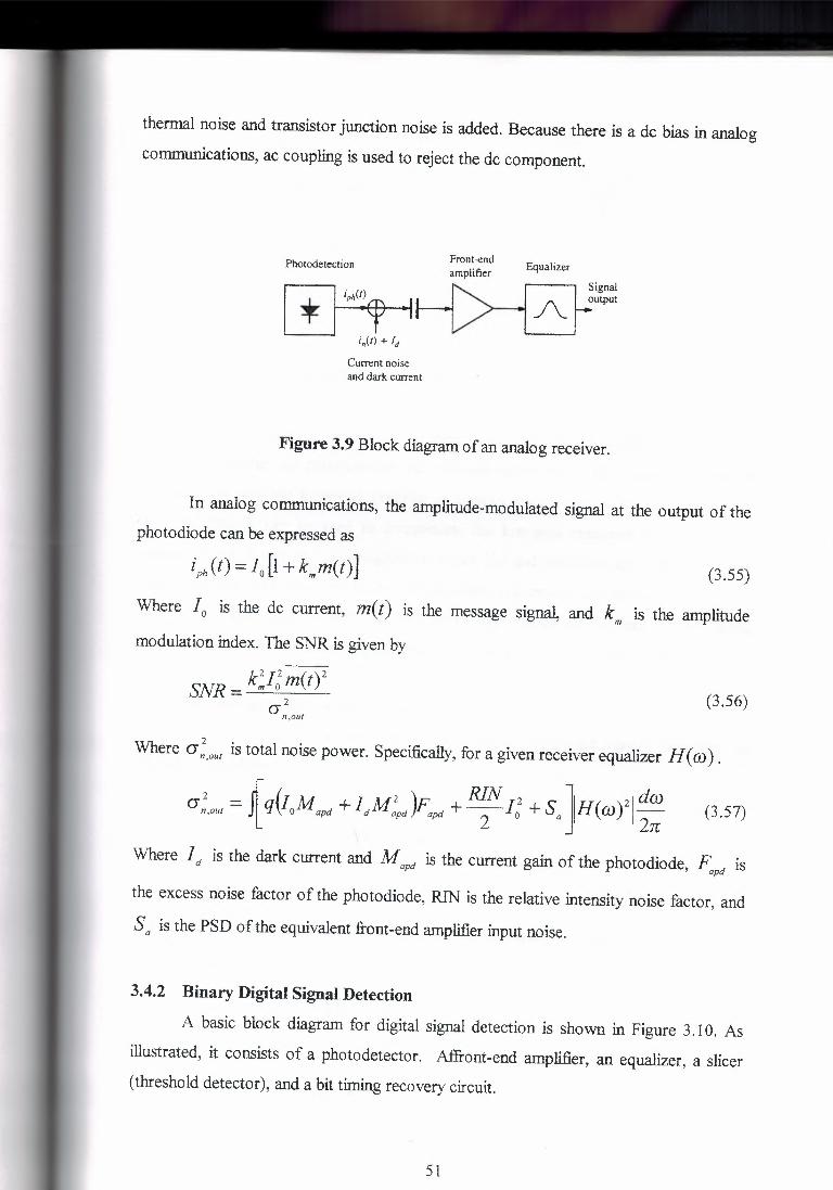
thermal noise and transistor junction noise is added. Because there is a de bias in analog
communications, ac coupling is used to reject the de component.
Photodetection Front-end amplifier Equalizer
Signal output
Current noise and dark current
Figure 3.9 Block diagram of an analog receiver.
In analog communications, the amplitude-modulated signal at the output of the photodiode can be expressed as
': (t) = I0 [1 + k"'m(t)] (3.55)
Where I0 is the de current, m(t) is the message signal, and km is the amplitude
modulation index. The SNR is given by
SNR = k~I; m(t)2 0"2
n,out (3.56)
Where o :,out is total noise power. Specifically, for a given receiver equalizer H (co) .
2 _ f (l M I M2 'Ir. RIN 12 S ]/H( )2/dm un,out - JLq o apd + d apd/I'apd +-2- o + a m
2rc (3.57)
Where 1 d is the dark current and M apd is the current gain of the photodiode, Fapd is
the excess noise factor of the photodiode, RIN is the relative intensity noise factor, and
Sa is the PSD of the equivalent front-end amplifier input noise.
3.4.2 Binary Digital Signal Detection
A basic block diagram for digital signal detection is shown in Figure 3 .10. As
illustrated, it consists of a photodetector. Affront-end amplifier, an equalizer, a slicer (threshold detector), and a bit timing recovery circuit.
51

Front-end Threshold Photodetection amplifier Equalizer detection
Detected
* I pn~-$ 1 >-rl _/\_ H s I _ output
Current noise and dark current JUlJ-------l
Bit timing recovery
Figure 3.10 Block diagram of a typical digital receiver.
The photodetector converts incident light into photocurrent. The front-end
amplifier amplifies the photocurrent with minimal added noise. The equalizer is used in
combination with the front-end amplifier to achieve a certain receiver transfer function.
For example, it can be used to compensate the low-pass response of the front-end
amplifier, and it can also be designed to reduce ISI and maximize the SNR. The slicer
performs threshold detection. In the case of binary transmission, it detects the equalized
output as either high or low. To regenerate the original bit stream, the bit timing
recovery circuit recovers the original transmitter clock from the received signal.
3.4.3 Intersymbol Interference and Noise Formulation
If the front-end amplifier and equalizer have a combined transfer function, the output of equalizer is
Yout (f) = '; (f) Q9 h(f)
The signal component of the output signal is
def
Ys (f) = ipJf) Q9 h(t) = "f..Akp(( - kI'a) Q9 h(f) = "f..Akpout (t- kI'a) (3.58) k k
To detect the transmitted amplitude Ak, Yout at the equalizer output is sampled at the
bit rate and compared with a threshold. From equation ( 4.58) def
Yaut,k = You, (n; + r) = Ak Pout [O] + ISik + Yn,k (3.59) Where the constant dark current term has been dropped for its irrelevance.
(3.60)
52

def
Yn.k = Yn.our (kY'a + r) The error detection probability is
PE= PoP(yout,k > Y1h j Ak = AJ + PiP(Yout,k < Y11i j Ak =AH) (3.61) The two-sided PSD at the photodiode output is
Sn.out (w,t) = q~ph (t)Mapd + ldM:d ]F:pd + m; i;h + SMPN (co)
The total noise power at the equalizer output is
(3.62)
(3.63)
3.4.4 Bit Error Rate Neglecting Intersymbol Interference
To understand BER evaluation, let us first consider the simple case where ISI is
neglected. A power penalty can be subsequently added when ISI is included.
Using equation (3.59) and dropping the ISI term. We find the sampled output at the equalizer output is
You1,k = AkPauJO]+ Yn,k
From Gaussian approximation and equation (3.61), BER is
P, = p,{ y H IT~Y,,) + p,{ y •IT~ Y, ) Where YH = AHpourfo], YL = Alpourfo], Yrh is threshold, and cr;,cr; are the
(3.64)
corresponding noise power at Ak = AH and AL, respectively.
3.4.5 Bit Error Rate Including IntersymboI Interference
The BER is calculated by neglecting the ISL Now the effective ISI is included and a more rigorous· BER expression is derived.
Because both ISI and noise are signal dependent, the detection error probability
depends on input sequence. For accurate error probability calculation, the detection
error probability must be computed for each possible input sequence case and a
statistical average is taken, When ISI is a function of many adjacent symbols, this can
be tedious process. For simplicity, one may consider only the worst case. That is,
consider only the input sequence that gives the large error probability.
53

If the y n,k is assumed to be Gaussian, the BER reduces to
(3.65)
The output noise power can be decomposed as def
(52 = (52 + (52 n.out sd si (3.67)
3.5 Optical Amplification
Power loss in the fiber transmission places a fundamental limit on the speed and
distance product. When various couplings and splittings are used in an optical network
or a photonic switch, power loss can also limit the network size and switch throughput.
To overcome power loss problem, optical amplifiers can be used. Compared to
electronic amplifiers that amplify electrical signals, optical amplifiers have several
important advantages. First, they have a much larger amplification bandwidth. An
optical fiber amplifier, for example, can have a bandwidth of several thousand GHz.
Therefore, they are attractive to all-optical networking, where speed bottlenecks from
electronics are removed by optics implememation. Second, optical amplifiers can
amplify multiple optical inputs at different wavelengths simultaneously. Therefore, they
are attractive to applications such as wavelength division multiplexing (WDM).
3.5.1 Semiconductor Amplifiers
As mentioned earlier semiconductor amplifiers are laser diodes that are biased
below the threshold current. To provide amplification, the active layer of a
semiconductor amplifier has positive medium gain but not large enough for laser
emission.
(a) External pumping and rate equation
Similar to laser diodes, a positive optical gain in semiconductor amplifiers
comes from external current injection. From the rate equation of the carrier density
given by equation (3.23),
aN(t) =Rp(t)-Rs(t)- N(t) = J(dt) -rvga[N(t)-N1h]Nph(t)- N(t) (3.68) r, q r,
\Vhere
54
R/t) = J(t) qd
is the external pumping rate from current injection.
Rs(t)=ravg[N-Nth]Nph
Where
def 1 Nph,sat = ravgrr
is called the saturation photon density.
And
go g(N) = 1 + Nph I Nph,sat
is the gain of the amplifier.
Where
is called medium gain at zero photon density.
(b) Amplifier gain
When the medium gain is known, the light power P(z) is determined by
following differential equation
dP(z) =g(N)P(z) @
From gain saturation is considered from equations (3.72) and (3.74),
P(z) dP = g(z)P(z)dz = godz 1 + P(z)/ P,a1
Where P,a1 = N ph,sac ( hf)( wd)v g is the saturation optical power.
So
g @=[-1-+_1 ]dP o P(z) t':
integrating above equation from z=O to z=L gives
55
(3.69)
(3.70)
(3.71)
(3.72)
(3.73)
(3.74)

(3.75)
Equation (3.75) can be rearranged as
l Olog., (GO,no-sat J ~ 4.34 pin Go Go P;
(3.76)
This given equation shows the gain penalty in dB is linearly proportional to the actual
amplifier gain G0 and the power ratio P; I P,01•
(c) Fabry-Perot amplifiers
Because the two cavity facets of an amplifier an cause reflections, incident light
can be bounced back and forth within the amplifier. Amplifiers that have strong internal
reflections are called Fabry-Perot (FP) amplifiers.
To find the amplifier gain of FP amplifiers, assume a certain optical power
distribution P(z) in the cavity.
(3.77)
Equation (3. 77) can be simplified as
(3.78)
with z
G( )def f gcz')dz'
z =eo (3.79)
Once P(z) and G(z) are solved, from equation (4.78), the net amplification gain
of the FP amplifier is
G =(l-r2)(1-r2)\E+(L)\2 =(l-r2)(l-r2) Go FP L R p L R I j2f3L I
in 1- G0rRrL e (3.80)
3.6 Noise in Optical Communication When the transmission channel is not ideal, the waveform of transmitted signal
is distorted. As a result, the transmitted signal cannot be perfectly recovered, and it is an
important task to minimize the effects of noise and distortion at the receiver end. In
56

analog communications, this means maximizing the signal-to-noise ratio (SNR); m
digital communications, this means minimizing the bit error rate (BER).
In optical communications, noise can come from both the transmitter and
receiver. In addition to thermal noise, which occurs in essentially every electronic
circuit, there are phase noise, relative intensity noise (RIN), and mode partition noise
(MPN) from the light source at the transmitter side, and shot noise and excess
(avalanche gain) noise from the photo detector at the receiver side.
There are additional noise sources in advanced systems. For example, when
optical amplifiers are used to overcome power loss, they add so-called amplified
spontaneous emission (ASE) noise to the amplified signal. In the wavelength-division
multiplexing (WDM) and subcarrier multiplexing (SCM) systems in which multiple
channels are transmitted through the same optical fiber, there can also be adjacent
channel interference (ACI) or crosstalk, which is the interference from adjacent
channels because of the power spectrum overlap. Because adjacent channels are
statistically independent of the channel tuned to, they can be considered as another noise
source.
In addition to noise and crosstalk, there can be signal distortion because of a no
ideal channel. In optical communications, distortion can come from fiber dispersion and
device nonlinearity. Depending on the format of the signal transmission, channel
distortion results in different effects.
Unlike thermal noise, most sources in optical communications are signal
dependent. That is, when the signal level increases, the noise level also increases. For
example, shot noise power is linearly proportional to the photocurrent generated. Relative intensity noise and mode partition noise power are even worse, being
proportional to the photocurrent squared.
3.6.1 Effects of Noise and Distortion
To know the noise effects quantitatively, consider a basic point-to point
communication system. Let the transmitted signal be s(t), the channel impulse response
be h(t), and the channel noise be n(t). The received signal r(t) is thus given by def
r(t) = s(t) 0 h(t) + n(t) = q(t) + n(t) (3.81) def
Where 0 denotes the convolution and q(t) = s(t) 0 h(t) .
57
If the channel is ideal, it introduces only a certain delay and loss. Therefore, the
impulse response of an ideal channel is given by
h(t) =ao(t-r) (3.82)
Where a is a constant factor representing transmission loss (if a<l) and r is the
propagation delay. When h(t) is not ideal, equation (3.81) shows that received signal is
corrupted by both noise and channel distortion.
(a) Effect in analog communications
In analog communications, the received signal quality can be characterized by
the following ratio:
~ E[s(t)2] YQ -
E(is(t) - r(t)i2) (3.83)
Where E[x] denotes the expectation or average of signal x. Therefore, Els(t)2 J is the
average signal power and E~s(t) - r(t)/2) is the mean square error (MSE) with respect
to the original signal s(t).
When the channel is ideal, y Q reduces to the signal-to-noise ratio (SNR) given
by
Y Q = SNR = E s(t)2 E n(t)2 (3.84)
Where Eln(t)2 J is the average noise power.
(b) Effect in digital communications
In digital communications, the consideration is a little bit different. Instead of
minimizing the MSE, the objective is to recover the original bits transmitted with a
minimal error detection probability. Consider a pulse amplitude modulated (PAM)
signal transmitted over a channel. The received signal is given by
r(t)= z..Akp(t-kT0)+n(t) k
(3.85)
Where A;; is the amplitude of the kth pulse, p(t) is the received pulse, and T0 is
the interval between two consecutive pulses. To detect the transmitted amplitude A.t,
58

the received signal is first sampled at (kT +r) for a certain r within (O,T0). From
equation (3.85), the sampled output is
(3.86)
def def
Where A =p(iT+r) and nk =n(kT+r). Equation (3.86) shows that the
sampled output consists of three terms: signal ( Ak ), noise (nk), and distortion
( Ii"'k Aipk-i ). In digital communications, the last distortion item is called the
intersymbol interference (ISI) because adjacent symbols and pulses cause it.
Because of noise and ISI, r, and A.1: are not necessarily the same. A digital
receiver thus needs to guess what amplitude is transmitted from the received rk . The
process of finding a likely A1: from the sampled value rk is called detection. If Ak
= Ak, detection is correct; if Ak :t:- Ak, detection is incorrect. Because both noise and
ISI are unpredictable, the detection performance is characterized by the error detection probability:
A
PE ::::: P( Ak ::j:. Ak h) (3.87)
Therefore, the smaller the error detection probability, the better the transmission performance.
3.6.2 Noise and Distortion Reduction Techniques
When the power spectral densities (PSD) of a signal and noise are known, we
can use filtering and equalization techniques to reduce the effects of noise and distortion.
(a) Wiener filtering in analog communications
In analog communications, the objective is to maximize the performance
measure given by equation (3.83). To achieve this, a filter called an equalizer following
the receiver front-end is commonly used. From the received signal given by equation
(3.81), the equalized output is
59
def
rout (t) = r(t) ® »; (t) = q(t) ® heq (t) + n(t) ® heq (t) = S out (t) + nout (t) Where heq(t) is the impulse response of the equalizer. Therefore, the MSE is
Where the noise and signal are assumed to be statistically independent. The two
terms on the right hand side can be written as
and
def {i 2) 2 dOJ MSES = E~sout - s(t)j = [s, (OJ )!H(OJ )He/OJ)- II -
2rc
Where S, (OJ) is the PSD of the original signal and H(OJ) is the transfer
function of the channel. Let H0P1 be the optimum transfer function of the equalizer that
gives the minimum MSEs.min. If Heq = H0p1 + 8H, by expanding the factor
!H(OJ )H.q (OJ )-ij2, the MSE reduces to
A1SE = MSErmn + 91{ f[snH:pt + SsjHi2(H:pr -1)}H dOJ} + f(sn + SsjHj2 )8Hl2 dOJ 2n 2rc
Where 9t {z} denotes the real part of z. Because the last term on the right hand
side of the above equation is always positive, the middle term should always be zero to
ensure MSE 2:'.. MSEmin for any 8H . As a result, the optimum H opt (OJ) satisfies the
following condition:
or
(3.88)
The optimum filter by equation (3.88) may not necessarily be implementable
(i.e., its inverse Fourier transform may not necessarily have a finite duration).
Therefore, it is called noncausal Wiener filter.
60

(b) Matchedfiltering in digital communication
In digital communications, instead of minimizing the MSE as in analog
communications, one must minimize the error detection probability PE. If a similar
equalizer h.q (t) is used after the receiver from end, the filtered output from equation
(3.85) is
rour(t) = LA>:Pout(t-kTo)+nout(t) k
Where pout (t) = p(t) ® heq (t) . If we sample the signal at every T0, the sampled output
at (k + l)T0 is
Where we define r0ur,1c = r0uc[(k + l)T0] and n0ur); = n0uc[(k + l)To]. In the above
expression, pout (JT0) terms for j :t:- 1 are ignored. Because the filtered noise n0ut,k is
still Gaussian, so
To minimize PE' pout (To) IO" n must be maximized or out
[PourCTa)]2 = If P(ro)He/ro)e1w:0dro/(2n)/2 O" 11our f S,, ( (1) )/He/ (1) )\ dos /(2n) (3.89)
Where P(ro) is the Fourier transform of p(t). If H.q (oi) = H pre (w )H post (or) such that
(3.90)
then
According to Schwartz inequality,
Ip ourC T0)]
2
~ _l ]P( ro) H ,,, e'"'0 I' dro ~H - ( ro JI' dro = f IP( ro JI' do: l O" nout 2n ]H post ( (1) f dto Sn ( (1)) 2n
The equality holds when Hpost(OJ) = KP* (OJ )H;re(w )e-jmTo for some constant K.
Therefore, the optimum H opt ( co) is
61

(3.91)
This optimum filter is called the matched filter.
3.6.3 Shot Noise from PIN Diodes
The photocurrent from a PIN diode is constant when the incident light power is
constant. In practice, because of random EHP generation, the photocurrent has a random
fluctuation from its average value. This random fluctuation is called shot noise and is
the most fundamental noise in optical communications.
(a) Power spectral density of shot noise
Shot noise nshot (t) as a function of time at the photodiode output is defined to be
def
nsho1 (t) = i ph (t) - I ph (3.92)
Where i ph (t) is the photocurrent and I ph is its average. The two-sided PSD of a
shot noise is given by
(3.93)
Where Id is the dark current and H pin ( co) is the Fourier transform of the
impulse response of the PIN diode due to an HER. Because H pin ( «i) is generally flat
over a large frequency range, it can be dropped from equation (3.93). In other words
shot noise can be considered as a white noise over most relevant frequency ranges. If
this is the case, the shot noise power over a bandwidth Bis
-2- dto n,-nul = fs sho! (oi) x 2n ~ 2q(I ph + Id )B = 2q(RP;,, + l d )B (3.94)
3.6.4 Thermal Noise Thermal noise, a white Gaussian noise, is one of the most common kinds of
noise encountered in communication systems. Thermal noise is caused by radiation
from random motion of electrons. Because it is a Gaussian noise, the probability density
function (PDF) of thermal noise is Gaussian. This Gaussian distribution comes from the
fundamental central limit theorem, which states that if the number of noise contributor
62

is large and they are statistically independent, the combined noise distribution is
Gaussian. From thermodynamics, the PSD ofthennal noise is given by
S co _ hw (! + 1 ) . T( )- 2n 2 ehm/2rrJ:T -]
(3.95)
Where k is the Boltzmann constant and Tis the temperature in Kelvin. The first
term in equation (3.95) is from quantum mechanics. When kT >> ht» I 2n- , the power
spectrum is almost a constant and equal to kT . From this approximation, thermal noise
is a white noise with the following PSD:
(3.96)
The inverse Fourier transform gives the following autocorrelation for thermal noise:
(3.97)
If the noise is filtered over a finite frequency band B, the filtered power
spectrum will be zero outside the frequency band, and the average power is
CJ2 = Rr(O) = f kTdf = 2kTB .lrequency bands
(3.98)
Thermal noise can be modeled as a voltage source of bandwidth B by: 2
vthermai = 2kTB 2R
(3.99)
Therefore, we have
vr!ennal = 4kTRB (3.100)
In equation (3.99), the factor of 2 in the denominator on the left-hand side is to
account for the optimum power transfer efficiency. That is, 50 percent of the noise
power from the equivalent voltage source contributes to the measurable noise power
2kTB. The thermal current source can be similarly expressed as
(3.101)
Where G=l/R is the conductance.
If the thermal noise is included with the shot noise discussed earlier, the SNR at
the photodiode output can be expressed as
(3.102)
Where Vr = kT I q is the thermal voltage and G is the conductance of the load resistor.
63

3.6.5 Relative Intensity Noise in Laser Diodes
, Relative intensity noise is the intensity fluctuation at a laser diode output.
Similar to phase noise, it is primarily caused by random spontaneous emission.
Different from phase noise, which is critical to coherent communication and soliton
transmission, RIN is important in analog communications, such as in SCM (subcarrier
multiplexing). If incident light to a light detector has power Pin +Min, where ~n is
the zero mean intensity noise, RIN is defined as
def E1M.2 j 2S RIN = l m = __!!!!_ BP~ I';~
(3.103)
Where Bis the bandwidth of the signal and Snn is the two-sided PSD of Af>;n (t).
Because the photocurrent at the photodetector output is proportional to the incident light
power, the mean square of the photocurrent fluctuation can be written as
(3.104)
In addition to spontaneous emission, laser RIN can also be caused be modal
instabilities and reflection at the diode-fiber interface. Therefore, RIN can be factored
into two components: intrinsic RIN, which is caused by spontaneous emission and
internal modal instabilities, and extrinsic RIN, which is caused by reflection.
3.6.6 Phase Noise from Laser Diodes
As mentioned earlier, phase noise is caused by random spontaneous emission in
a laser diode. If there is no spontaneous emission, the output light spectrum consists of
delta functions. When there are random spontaneous emissions, the spectrum is no
longer a sum of delta functions. Instead, the spectrum is broadband and has a finite
nonzero linewidth around each w; .
(a) Linewidth broadening because of phase noise
To see the effect of linewidth broadening, consider a continuous wave light
output of a single-mode laser given by
x(t) = eJ[wc1~(t)j (3.105)
Where we is the center frequency and ¢(t) is the phase noise. If ef>(t)= 0, x(t) is
at a single frequency and its PSD is a delta function. When there is phase noise, the PSD
due to phase noise is given by
64
(3 .106)
Where Rsp is the spontaneous emission rate (11sec), a1w is the linewidth
broadening factor (1/sec), I is total number of photons in the laser cavity, and tcoh is the
coherence time given by def 41
t ------ coh - Rsp(l+aJw)
(3.107)
Equation (3 .107) shows that t coh is proportional to I, or the output optical
power. Therefore, the larger the optical power, the larger the coherence time. The
spectrum given by equation (3.106) is commonly referred to as a Lorentzian spectrum.
I ts FWHM bandwidth is
2 2Rsp ( 2 ) firo3d.B = -t- = -- 1 +a1w
coh 41 (3.108)
Therefore, the larger the output optical power, the smaller the 3dB linewidth.
Good single-frequency laser diodes today can have a 3dB bandwidth around 100 kHz.
(b) Phase noise in coherent communications
In addition to the linewidth broadening effect discussed above, phase noise can
directly corrupt the phase or frequency of a modulated carrier in coherent
communications. The phase noise ¢(t) given by Equation (3.105) consists of two
components: one deterministic that results in a frequency shift from ro c and one random
that broadens the linewidth. Because a constant frequency shift has no effect on phase
or frequency modulated carriers, only the random phase component must be considered.
Denote it by ¢, (t). The autocorrelation of the time derivative of¢, (t) is given by
(3.109)
By taking Fourier transform, the corresponding PSD is
s ~r (co) = l:iro3dB (3.110)
Because <f> r is the time derivative of <f,,(t), the PSD of the phase noise is
(3.111)
65

Since the time derivative of a phase is frequency, <Pr represents a frequency
noise. Equation (3.110) shows that the frequency noise caused by shot noise is a white
noise, and when FSK is used the frequency separation must be large enough compared
to !im3dB. On the other hand, equation (3 .111) shows that the phase noise is
proportional to 11 /2, which means a strong noise in the low-frequency range. When
phase modulation is used, the bit rate must be high enough that the effect of phase noise can be minimized.
3.6. 7 Mode Partition Noise
Mode partition noise (MPN) is caused by mode competition inside a multimode
FP laser cavity. As a result, even though the total power is constant, the power
distribution over different modes is random. Because different modes have different
propagation delays in fiber transmission, random power distribution results in random
power variation at the receiving end. This power fluctuation due to mode competition is called MPN.
Because the power competition among all longitudinal modes is not fully
understood, an exact description of the PDF is not available. However, similar to RIN, it
is well known that the noise power of MPN is proportional to the signal power. As a
result, an error floor can be reached when MPN becomes dominant.
Suppose a given laser diode has N longitudinal modes and each has a relative
power a., i = l, ,N. By definition, the sum of these a1 's satisfies
(3.112)
Because each a1 at a certain time is random variable, the average relative power
for mode i is given by
a1 = E[a1] = f a1 x PDF(ai, ,aN )da1 •••• da.,
If the waveform of mode i received is J; (t), the combined received signal is
(3.113)
If the signal is sampled at time t0, the variance of the sampled signal is
cr2 = E~(t0)2 ]-E[r(t0)]2 (3.114)
66

From equations (2.33) and (2.34),
cr2 = Z:.,J;Uo)f1(to)(a;a1 -a;a) i,j
(3.115)
To simplify the expression, Ogawa introduces a constant kmpn, which is defined as
2 def Li ,j [t; (to) - fj (to) f (-;;;; - -;;;; ) def N
kmprr = '°'· [J~(to)- f1(to)f a;a, = D ~I,) •
(3.116)
Where
= LJ;(to)2a; -2LLJ;Cto)f1Cto)a;aJ + Lf/to)2a1 i j J
(3.117)
and
i,j
= I[t;(to)2-2_(;(to)f/to)+f1(to)2}a;a1 -a;a) i,j
i,j
= 2cr2 (3.118)
Therefore, from equations (3 .115) and (3 .118),
cr2=k2 x-l-xcr2=k2 Dcr2=k2 D mpn k2 mpn N mpn 2
mpn
(3.119)
Because a; is the average power distribution, which can be measured
experimentally, the last expression for o 2 is a convenient form to compute cr 2 at a
given kmpn.
67

3.6.8 Avalanche Noise in APDs
Because of multiplication and avalanche process, the photocurrent generated by
an APD has an even larger fluctuation. This larger fluctuation comes from the random
secondary EHP generation by each primary EHP. The total noise is called the APD
noise, and the contribution from the random secondary generation is called the excess
noise, which is quantified by a factor called the excess noise factor.
The APD noise power over frequency range B is
(3.120)
Where M apd is APD gain and F apd is excess noise factor.
3.6.9 Noise from Optical Amplification Because spontaneous emission comes together with optical amplification,- noise
is added when a light signal passes through an amplifier. As mentioned earlier this noise
is called the amplified spontaneous emission (ASE) noise because it is also amplified.
(a) Amplified spontaneous emission noise
Photons that contribute to the ASE noise can have different transverse modes in
the amplifier and different polarizations. The one-sided power spectral density of the
ASE noise that is of the same mode and polarization as the incident light signal was first
derived by Kogelnik and Y ariv and can be expressed as
s ASE(!)= (G - l)nspxhf (3.121)
In the expression, G is the amplifier gain, hf is the photon energy, and
N2 n =--=-- sp N2 -NI
is a parameter describing the external pumping that depletes the ground state
(3 .122)
population.
3.6.10 Total Noise
The above discussion presented various kinds of noise in optical
communications. Now let us check their total effect on final signal detection. As
68
illustrated in figure 3 .11, the total noise at the photodetector output and front-end amplifier input is
ntot (t) = nmpn (n) + nrin (t) + napd(t) + nth (t) (3.123)
If a PIN diode is used instead of an APD, napd (t) should be replaced by nshot (t).
Because phase information is not detected in direct detection, phase noise is not included in equation (3.123).
Light source Photo detector Front-end amplifier
Channel
R[N ,mdMPN Shot noise Thermal or APO noise noise
Figure 3.11 Total current noise at the photodetector output.
69
CHAPTER4
NETWORKING
Because of the fast growing needs of networking services and rapid
development of supporting technologies, light wave technology research and
development have expanded from point-to-point transmission to high speed networking
over the last decade. This expansion is very critical to many broadband services, such as
interactive video, medical imaging, and distributed computing that need not only high
speed transmission but also networking support such as medium access and switching.
In optical networking, there are different system considerations and design
trade-offs because of different high-speed and optical implementation characteristics.
2.1 Time-Domain Medium Access When the form of the shared resource is in time, frequency, or code, we have
time-domain, frequency-domain, and code-domain access, respectively. To access the
shared medium in the time-domain, a transmission node needs to know when and how
long it can send its data. One sample approach is to divide time into frames and partition
each frame into a certain number of time slots. In this way, communication nodes can
share the same medium by sending data in different slots. Once a slot is allocated during
the call setup, a node can repeat the transmission in the same slot of each frame
throughout the call duration. This is called deterministic access and there is no traffic
contention after the call setup. Data transmission in two adjacent slots can be continuous in bit timing or
separated by guard time. To transmit data in different slots continuously, bit timings
from different sources first need to be synchronized. This medium access scheme is
called time division multiplexing (TDM). When a network is used for multiple access, it
is impossible to synchronize the timings of all nodes distributed over the network. As a
result, guard time that separates consecutive slot transmissions is necessary, and the
medium access scheme is called time division multiple access (TDMA).
Because TDM requires bit timing synchronization, its implementation is more
involved. To synchronize input bit rates, electronic implementation has to be used and
direct optical domain multiplexing is not practically feasible. A TDM standard called
Synchronous Optic Network (SONET) has been designed for optical transmission. To
70

avoid the electronic bottleneck in high speed multiplexing, SONET introduces an
innovative :floating payload concept that can synchronize input signals at low speeds.
Because of no need for bit timing synchronization, TDMA can be done directly
in the optical domain. An optical transmitter in this case gets access to the medium by
transmitting an optical burst consisting of binary bits over a time slot. When all optical
networking is concerned, TDMA is an attractive choice compared to TDM. However,
TDMA has a worse access efficiency than TDM because of the guard time.
In addition to TDMA and TDM, token passing and random access can do time
domain medium access. An important token passing fiber based local area network is
called the Fiber Distributed Data Interface (FDDI).
4.1.1 Time-Division Multiple Access As illustrated in Figure 4.1, a TDMA frame consists of a reference burst and a
certain number of time slots. The reference burst is used for frame synchronization,
signaling, and the time slots are used to carry data.
The reference burst consists of three parts: a preamble, a start code, and control
data. The preamble is a periodic bit sequence for bit timing synchronization. Depending
on how rapid synchronization can be achieved, the preamble length can range from 10
to several hundred symbols.
J>:.Pftamblc: S:•Sta.rtoc,da C, C'>ntrol 4/Ua Pi..: ·1;i1ormaJl~I! payl15od
Figure 4.1 A TDMA frame consisting of N slots
Once the bit timing is established, the content in the rest of the reference burst
can be read. Following the preamble is a unique start code indicating the end of the
preamble and the start of the information portion of the reference burst. By recognizing
71

the word, control data can be interpreted correctly; In general, control data carries
information such as station timing, call setup status, and signaling information. The reference burst in a TDMA frame is the overhead and occupies only a small
portion of the frame. The rest of the frame is divided into time slots separated by guard
time. Similar to the reference burst, each time slot consists of a preamble, a unique start
code, and the information payload. Because of different propagation delays between
stations, the guard time between time slots is necessary to avoid overlap between two
consecutive time slots.
( a) Shared medium Consider a TDMA network made of a shared medium where a node can
immediately receive what it just transmits. A single Ethernet coaxial cable and an
ALOHA radio network are examples of such a shared medium.
Figure 4.2 Required guard time of a shared TDMA network.
(b) Medium access and time compression When nodes attached to a TDMA network have data to transmit, they need to
wait for available time slots. In TDMA, a slot is obtained through a call setup process.
72

Once a node is granted with an available slot, it can use the same slot in every frame
throughout the call. As mentioned earlier, this medium access is called deterministic.
Because of the deterministic access, TDMA is primarily used for constant bit
transmission. To support such transmission, input bits of a constant bit-rate signal are
tip; Stored in a transmitter buffer. When the assigned time slot arrives, all the bits stored
will be transmitted at a much higher speed. This process is illustrated in Figure 4.3.
Clearly, data bits are compressed in time during the high-speed transmission. For this
reason, TDMA also called time compression multiplexing.
First-in-first-out buffer
Buffer size = BT1
111111. I- r1 --1 Time
(m bits)
I • T _[ \- Time s.phx~
(m bits)
Figure 4.3 Concept oftime compression multiplexing in TDMA.
From the compression mechanism described, the payload size of a time slot can
be determined for a constant bit-rate input. For input signal of a bit rate Bs bis, the total
number of input bits during a time frame is T1Bs, where T1 is the TDMA frame size.
To transmit bits over the payload oftime slot, payload size Ts.pload should be at least
Bs T -T- f,ptoad - 1 R
(4.1)
(c) Slot size, compression delay and access efficiency In addition to its payload, a time slot has an overhead for synchronization and
signaling. Therefore, the time slot size Ts is
Ts = Ts ,ah + Ts .pload (4.2)
73

Where Ts oh is the overhead size for preamble, signaling and control.
From equation ( 4.2) and ( 4.1) the time slot size is
Bs Ts = t.; + Tf R At a given reference burst size Tref and guard time Tg , the total number of time
(4.3)
slots that can be accorrnnodated within a frame is
[Tf - Tref J R 1- T,ef I Tf
N= T5+Tg = B, l+(R/B5)(Ts,oh+Tg)/T1
From equation (4.4), note that N has an upper bound of RI Bs and can be
(4.4)
improved by increasing T1 . At a given Tg, T,ef, Ts .oh : RI Bs , the upper bound can be
approached when T1 >> Tref and T1 >>(RI Bs )(Ts.ah + Tg).
At a given N, the access efficiency is defined as the ratio of the total data
transmission time to the frame size. From equation ( 4.4 ),
NTS,pload NBS B5 [ R 1-T,ef f Tf J TlwMA = T1 =R=R Bs l+(R/ Bs)(Ts,ah +Tg)/Tf
(4.5)
When T1 is large enough, the upper limit of the access efficiency is (B5 I R)LR! B5j.
4.1.2 Optical Domain TDMA In spite of the difficult trade-off mentioned above, optical domain TDMA is still
attractive because of no need to synchronize bit timings among transmission nodes. As a
result, as long as the receiver knows the transmission bit rate, each transmission node
can have its independent bit clock. Because the bit rate is usually high in optical domain
TDMA, this clock independence that avoids the need of bit clock synchronization
among transmission nodes is an important characteristic. The star topology is preferred to minimize the effect of guard time. A block
diagram of such an optical domain TDMA network is shown in figure 4.4. To
synchronize the access, master frame timing is needs to be distributed to all nodes. To
achieve this one of the nodes in the network is called master node, which generates a
reference burst every T 1 .
74

TOMA transmitter
\ Input data
Optical transmitter To other
High-speed instantaneous bit clock
From other
Transmitter slot timing
Master frame and slot timings
coupler
, Receiver
i -~-~~-~i"..g ............•................... . .
·----+··--··--··················•-·········-···············································-··················································--··················· Decompression
FIFO
Reference Low-speed read clock
Detection Data output
Bit timing recovery burst
processing Receiver
__ ..&.._f_ra_m~e timing Slot timing derivation
Receiver slot timing
····················-·········································· ·--.---·-···············-················-············· . TDMA receiver
Figure 4.4 An optical domain TDMA implementation.
To receive data over a certain time slot, a gating signal that is high during the
slot interval is generated from the derived slot timing. As illustrated in figure 4.4, data
in this slot interval can pass through the gate, be detected, and then be stored in the
decompression buffer. The received slot timing derived is also sent to the local
transmitter to determine its slot timing for transmission. Therefore, to have same frame timing at the star coupler, the additional delay
DA is added so that (4.6)
Where TM ,pg + TA,pg + DA is the relative delay of the transmitter frame timing at
the user node with respect to the master frame timing. From equation ( 4.6) (4.7)
75

Where m is the smallest integer such that mT1 - 2TA,pg > 0 . Equation ( 4. 7)
shows that a large delay line is needed when T1 is large to have a high access
efficiency.
4.1.3 Time-Division Multiplexing
TDM was first used in digital telephony, where multiple lower rate digital
streams called tributary signals are interleaved in the time domain to form a higher rate
digital signal. Similar to TDMA, TDM is time domain medium access scheme and each
of its frames consists of a certain number of time slots. However, different from TDMA,
data carried by different time slots are first synchronized in bit timing, and then
interleaved by a higher bit clock.
The process of bit timing synchronization is called frequency justification, which
is necessary when upstream signals have different bit clock frequencies.
Overhead Time :,;lots
+ ~ ~----
1 I I I I · · · I 1 .... "
Overhead
(a) One-dimensional frame structure
Time slots
/
(b) Two-dimensional frame structure
Figure 4.5 TDM frame formats.
The process of bit timing synchronization is called frequency justification, which
is necessary when upstream signals have different bit clock frequencies. Because all
76
laser diodes can operate only up to tens of GHz, parallel transmission from WDoMA is
a key to high utilization of fiber bandwidths.
4.2.1 Wavelength-Division Multiple Access In WDMA, wavelength channels are the shared resources. To access the
network, each source node needs to first acquire a wavelength channel. To ensure
proper transmission to the final destination, either the destination receiver must be tuned
to the wavelength channel or there must exist an efficient routing algorithm that can
forward data to the destination. Over the last few years, many access protocols and
routing algorithms have been proposed. In general, a good WDMA access protocol
should both perform satisfactorily and be easy to implement. That is, from the system
prospective, the protocol should achieve a high access efficiency, high throughput, and
low transmission delay. From the implementation prospective, the required tuning
speeds of tunable devices should be feasible, the number of total wavelength channels
needed should be attainable, and the channel allocation algorithm should be simple and
fast.
(a) Logical configurations and routing in fixed tuning WDA1A
When the traffic pattern in a WDMA network is stationary, fixed tuning is a
good choice to simplify the design and relax the fast tuning requirement. By choosing
the tuning wavelengths of individual transceivers properly, a WDMA network can have
a logical configuration independent of its physical connections. Once the logical
configuration is determined, simple and efficient routing algorithms can be derived.
(b) Dynamic tuning WDMA When the traffic pattern changes rapidly and high speed-tuning technology is
available, a more efficient medium access control is to allow transceivers to tune
dynamically. As a result, single-hop can be achieved by setting up a common
wavelength channel between the source transmitter and destination receiver.
From the logical configurations, note that a wavelength channel can be mapped
logically to spatial channel. Therefore, dynamic tuning in WDMA is in principle
logically equivalent to dynamic spatial switching. Consequently, borrowing switching
techniques used in packet switching networks can perform dynamic tuning.
78

(c) Frequency reuse
In a WDMA network where all wavelength channels are coupled in the
same-shared medium, the number of wavelengths required is
N).=pN (4.8)
Where N is the total number of nodes and p is the number of transceiver pairs
per node. Therefore, when N and p are large, the number of channels can be too large to
be implmentable.
Figure 4.6 Frequency reuse by wavelength partitioning.
To reduce the number of wavelengths required, the concept of frequency reuse
has been proposed. There are several approaches to achieving this. First, multiple shared
media can be used for wavelength isolation, As illustrated in figure 4.6, a logical
hypercube configuration can be implemented by partitioning wavelength channels into
three physical networks. As shown for a network size of 8, the number of wavelength
channels can be reduced from 24 to 8. As a result, frequency resolution is reduced by a
factor of 3. However, three separate sets of fibers, couplers, and splitters are needed.
4.2.2 Tunable Sources
WDoMA requires various advanced opto-electronic devices to implement carrier
generation, coupling, and tuning. In the last few years, many interesting and innovative
designs have been proposed.
79

In principle, discrete DFB, DBR lasers can be used as tunable sources
inWDoMA. However, in either WDM or WDMA, it is desirable to build a large tunable
laser array for cost effective implementation. In WDMA it is desirable to use a large
number of transceivers per node for high throughput and low transmission delay. In
WDM, a large laser array can also be integrated with multiplexing devices fir high-
speed transmission.
(a) Tunable laser arrays
For WDM applications, high speed and tunable laser array designs of sizes up to
20 lasers have been reported recently. Most laser arrays for WDM applications are
based on MQW and DBR combinations, where MQW is used as the active layer for low
threshold current a DBR is used for frequency tuning. A typical MQW-DBR laser array
is illustrated in figure 4. 7.
Active layer
Figure 4.7 An MQW-DBR laser array.
(b) Waveguide grating router and optical amplifier Another innovative design of tunable light sources has been proposed by
forming a positive feedback loop between optical amplifiers and the wave-guide grating
router (WGR). In this way, the WGR serves as an optical filter. When the net gain of
positive feedback loop is greater than unity or O dB, optical carriers with wavelengths
determined by the WGR can be generated.
(c) Frequency tuning and stabilization
As pointed out earlier, accurate wavelength generation is important to proper
wavelength multiplexing, interchannel interference, and tuning. The output wavelength
80

of a tunable laser, however, can vary because of fabrication errors, temperature, bias
current, and aging. A typical temperature coefficient of the output wavelength of a
single-frequency laser is around 0.09 nm/C",
One way to maintain frequency stabilization is to use an absolute frequency
source that is stable against various external conditions. In this approach, both channel
separations and absolute frequencies can be maintained for proper channel multiplexing
and tuning.
When the absolute frequencies are not required, it is only necessary to ensure
constant channel separation to avoid a large ICI. In this case, a single FPI can be used as
the calibrator.
4.2.3 Frequency Independent Coupling
Wavelength channels need to be coupled to the shared medium for transmission.
To allow a node in WDMA to tune its wavelength channels for transmission, coupling
should be made insensitive to the wavelength. For this purpose, a star coupler is
commonly used. A star coupler has N input ports and N output ports, with each output
port consisting of all signals from the N input ports.
In star coupler design, one important consideration is the total power loss. From
conservation of energy, when the coupler is symmetric, the output power of each
channel at each port is attenuated by at least a factor of N, the size of star coupler. This
1/N coupling loss is called distribution loss because the incident light from one input
port is distributed to N output ports. In addition to distribution loss, there is excess loss
due to many couplings with loss such as internal power attenuation. As a result, the total
coupling loss in a star coupler is
a10rdB = 10 l log.; (N) + a excess dB (4.9)
4.2.4 Frequency Dependent Multiplexing
In addition to star couplers, frequency-dependent multiplexers can be used to
mix wavelength channels. In this case there is no distribution loss. However, mixed
outputs are strongly dependent on wavelengths of input signals. Different from star
couplers, multiplexers are thus primarily used in WDM. In WDMA, where nodes can
tune their transmission wavelengths, use of frequency-dependent multiplexers is not
suitable.
81

To implement a frequency-dependent multiplexer, there are two pnmary
designs: grating and Mach-Zehnder interferometry. In the first case, light from different
spatial directions is coupled together. In the later case, light of different wavelengths is
coupled together, with coupling coefficients dependent on the input wavelengths.
Grating is an arrangement that imposes on an incident light a periodic phase
variation. When many phase-shifted versions of the incident light are superimposed, a
spatially dependent intensity pattern is formed.
Another emerging and important design of frequency-dependent multiplexers is
based on Mach-Zehnder interferometry. In this approach, a N: 1 multiplexer is
composed of N -1 2 x 2 Mach-Zehnder interferometers in m stages, where N = 2 m •
4.2.5 De-Multiplexing and Optical Filtering
When incoherent detection is used, a mechanism is needed to select one of the
wavelength channels optically before photodetection. In general, this can be done in
either the spatial domain, frequency domain, or polarization domain. In the spatial
domain, wavelength channels are split into different spatial paths for detection. In the
frequency domain, either an optical band-pass filter is used to suppress out-of-band
channels or a narrow-band optical amplifier is used to amplify only the in-band
channels. In the polarization domain, a polarizing beam splitter separates a wavelength
channel if its polarization is orthogonal to that of other wavelength channels.
As mentioned earlier, there are two design criteria in de-multiplexing
wavelength channels: a large free spectral range (FSR) and a high spectral resolution.
The fundamental reason that two wavelengths at one FSR separation have the same de
multiplexed output is because wave interference has a periodic effect in phase. To avoid
ambiguity, a large FSR is required. In general, the FSR of a de-multiplexer is inversely proportional to the period of its grating or diffracting structure.
The spectral resolution of a de-multiplexer, on the other hand, determines how
closely two wavelength channels can be separated. In general, the resolution is inversely
proportional to the device size that introduces the wave interference. This can be
understood from the Fourier transform, which says that the larger the size of an object in
the spatial domain, the smaller the width of its Fourier transform in spatial spectral domain.
82

4.3 Photonic Switching
Switching is a network function that routes traffic from one channel to another.
To provide high switching throughputs and to avoid the electronics speed bottleneck,
photonic switches that implement the I/0 interface and switching fabric in optics, as
shown in figure 4.8, have been actively studied over the last decade. For fast packet
switching such as in B-ISDN/ A TM that needs high speed switching control, self-routing
photonic switches that integrate switching control with switching fabrics in optics have also been demonstrated.
Input interface
Output interface
Switching fabric
: l I: I ·I: I I : Switching control
Figure 4.8 A block diagram of a switch.
To simplify implementation of large photonic switches, 2-to-2 switches can be
used as the building block. In general, with a multistage interconnection architecture,
any switch size of 2k can be built. In addition, with a good interconnection architecture,
the number of 2-to-2 switching elements can be reduced while maintaining good switching performance, such as zero blocking probability.
Similar to multiple access, photonic switching can be done in different domains
such as space, time, wavelength and polarization, where traffic is switched from one
spatial line, time slot, wavelength channel, or polarization state to another. These
different domain switchings have different system characteristics and require different
83

physical implementation. For example, spatial domain switching can configure different
physical light paths but require complete spatial interconnections. Wavelength domain
switching, on the other hand, is attractive to WDoMA but requires precise wavelength
control and tuning.
Performing switching in multiple domains can reduce its complexity. For
example, by performing time-space-time (TST) switching, the number of spatial cross
points can be greatly reduced. In WDoMA network, spatial switching can be similarly
combined with wavelength channel interchange (WCI) to form a large switch. In
general, switching in different domains and their combinations can be logically
equivalent. For example, WCI is logically equivalent to time-slot interchange (TSI). As
a result, the most convenient technology can be used to implement the same logical
switching architecture and similar switching control algorithm can be used to achieve
the same switching performance.
4.3.1 Switching Architectures
Some important switching architectures that 2 x 2 switches as the basic building
block. Although 2 x 2 switches can be realized in different technologies, they can be
interconnected with the same architecture and similar system considerations.
(a) System considerations
There are several criteria for a good switching architecture from system
considerations. First, for a given switch size, N, the number of cross-points for 2 x 2
switches should be as small as possible. When the number is large, implementation is
expensive and the optical path is subject to large power loss and cross talk. As a result,
one primary design objective is to minimize the number of cross-points.
To evaluate a switch design from its number of cross-points, it can be compared
with the lower bound, log , (N!). This lower bound can be obtained from the following
consideration. Because a switch works as a permutator that routes inputs to outputs
according to a certain permutation, it needs to provide at least N! different
configurations. Because each cross-point can provide two different configurations, a
minimum number of log, (N!) cross-points are needed to configure N! different
routings or permutations.
84

Many switching architectures have been designed to minimize the number of
cross-points. The three-stage Clos switch is one example. Another switching
architecture, called the Benes network, can approach the lower bound asymptotically. If
internal blackings are acceptable, using a self-routing network can further reduce the
number of cross-points.
Optical paths should go through a minimal and equal number of cross-points.
Because each cross-point introduces a certain power loss and cross talk, a large number
of cross-points along a configured path require a large incident light power. Many
multistage switches have thus been designed to have as few as log, N cross-points along
any configured path. Furthermore, to reduce power variation at the switch output and to
avoid the near-far problem, optical paths need to have the same number of cross
points. When a switch is designed to reduce the number of cross-points in total and in
each configured path, it can have a large internal blocking probability. In a multistage
switch, internal blocking occurs when there is no available route from the existing
configuration. To reduce the blocking probability, the number of possible routes
between inputs and outputs can be increased. The Clos switch, for example, can have a
zero blocking probability when the number of middle-stage switches, which equals the
number of possible routes, is large enough.
In some switching architectures, the internal blocking probability can be
completely reduced to zero by using a good switching control or rearranging the current
switching configuration. These cases are called wide-sense non-blocking and re
arrangeably non-blocking, respectively. These different non-blocking conditions are
defined below.
Strictly Non-blocking: A switch is strictly non-blocking if a connection path can always
be found no matter what the current switching configuration is or what switching control algorithm is used.
Wide-Sense Non-blocking: A switch is wide-sense non-blocking if a connection path can
always be found no matter what the current switching configuration is if a good
switching control algorithm is used. In other words, the switch can have internal
blockings if a poor switching control is used but will have no blocking if a good
switching control is used.
Re-arrangeably Non-blocking: A switch is re-arrangeably non-blocking if a connection
path can be found by rearranging the existing switching configuration.
85

4.3.2 Spatial Domain Photonic Switching
In spatial switching, physical optical paths between input ports and output ports
are configured according to the requested connections. Three types of spatial switching
elements are then considered: mechanical switches, directional couplers, and bistable
optical gates. These switches configure optical paths by moving optical fibers, changing
the optical coupling characteristics of wave-guides, and modulating the states of bistable gates, respectively.
(a) Mechanical switches
A mechanical switch configures light propagation paths through a mechanical
mechanism. As shown in figure 3.12, an array of 1-to-2 photonic switches has a
movable portion so that input fibers can be coupled to one of the two output fiber
arrays. In general, multiple 1-to-2 and 2-to-1 switching elements can be interconnected to form a larger switch.
Because there is no need for advanced optics, a mechanical switch is attractive
for its simple implementation. As a result, it is good for use in cross-connects and
automatic protection switches (APSs) where the slow mechanical speed is not a
concern. Mechanical switches have some limitations.
Figure 4.9 A mechanical photonic switch connecting a fiber array to one of the two
output arrays.
86

When an input fiber is switched to different fiber, for example, there can be
larger coupling loss from misalignment.
(b) Waveguide switches
A more popular switch design is based on the directional couplers depicted in
Figure 4.10. As shown, coupled wave-guides provide the mechanism to switch incident
light from one wave-guide to another. An external voltage can be used to modulate the
refractive index of the wave-guides through the EO effect, which can in turn modulate
the light coupling between the wave-guides.
Input I
(a) (b)
Figure 4.10 A 2-to-2 waveguide switch using directional couplers.
4.3.3 Multidimensional Photonic Switching
In addition to spatial domain switching, traffic can be switched in the
wavelength domain and time domain. To switch light signals from different physical
lines, these different domain switching are commonly integrated with spatial domain
switching. For lower spatial switching complexity and better match with TDoMA or
WDoMA traffic, this integration into multidimensional switching is attractive.
(a) Wavelength domain switching
Wavelength switching is commonly used in WDoMA. According to how
wavelength channels are switched, there are two primary types: broadcast and select
and wavelength routing. As shown in figure 4.11, the first type uses a star coupler to
mix all wavelength inputs and broadcast them to all output ports.
87

Star coupler Tunable Wavelength filters converters
" A1 "2
• A2 • • .. ....• "-N AN
A1, Az, ··.,'AN
F!gure 4.11 A broadcast-and-select wavelen~h~wjJch~
Using optical filters at the star coupler outputs allows non-blocking wavelength
switching. To allow several wavelength switches to be used in series, wavelength
converters (_WCs '\ are added to q_erform necessarv wavelenzjh 1;1__ermutatian,
(b) Time domain switching
Time domain switching is attractive to TDoMA where traffic is multiplexed in
the time domain. Because photons cannot be easily stored and retrieved after a
programmable delay, implementation of time domain switching or time slot interchange
is not an easy task. A programmable time delay line that uses a fiber loop and a 2 x 2
photonic switch is shown in figure 4.12a. By designing a unit delay T in the fiber loop,
a programmable delay of multiple T's can be achieved by changing the state of the
2 x 2 switch. To do this, the switch is first set in the CROSS state for a duration of T to
switch the input packet to the delay loop. After that, the switch is set in the BAR state
for duration of (k - l)T, which then keeps the packet for another (k- l)T delay. At the
end, the switch is reset to the CROSS state, and a total delay of kT is introduced.
88
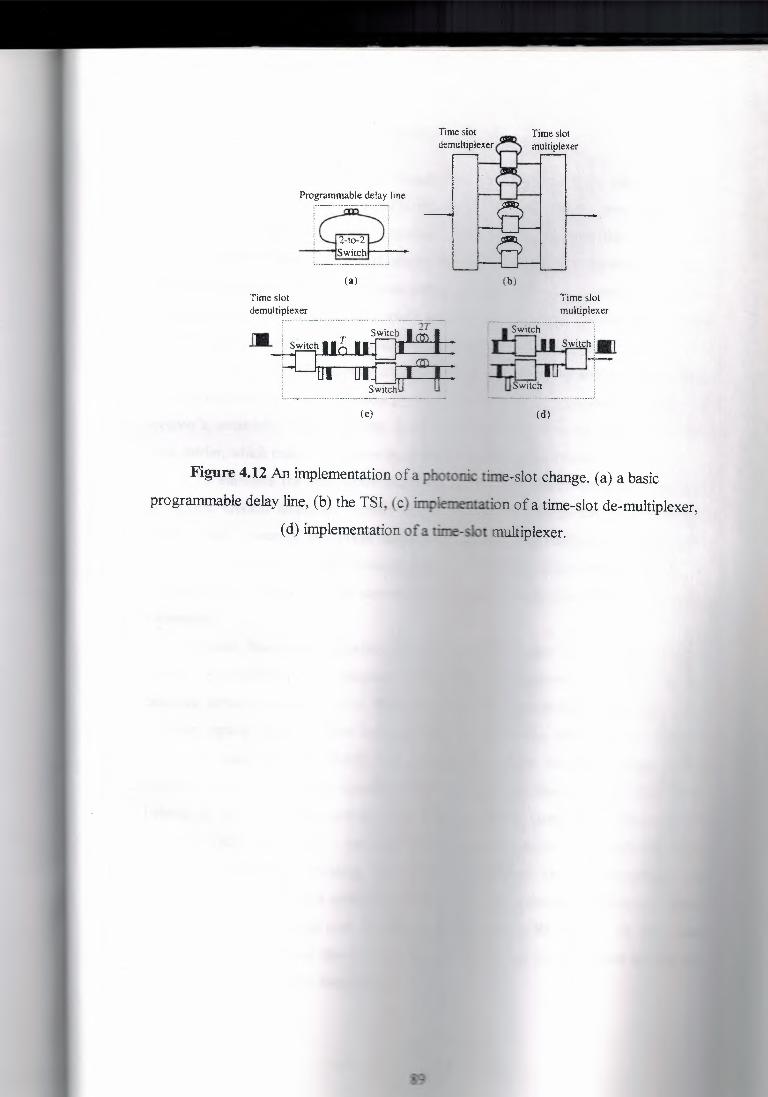
Programmable delay line
(a) (b)
Time slot demultiplexer
Time slot multiplexer
(c) (d)
Figure 4.12 An implementation of a photonic time-slot change. (a) a basic
programmable delay line, (b) the TSI, (c) implememarion of a time-slot de-multiplexer,
( d) implementation of a tirre-slot muhiplexer.
CONCLUSION
The development of optical communication technology has passed through
several generations. The two primary objectives of these efforts have been larger
transmission capacity and longer transmission distance. To improve the capacity and
distance, higher output power and smaller fiber attenuation are essential to longer
transmission distance, and good spectral coherence is key to higher transmission speeds.
Therefore, most efforts have been made to improve the output power and spectral
coherence of light sources and to reduce fiber attenuation and dispersion.
In early times, when optical communications was not well known, signals were
detected incoherently. But as the time passes coherent detection was used to enhance the
receiver's sensitivity. With coherent detection, received signals are amplified by the
local carrier, which makes the system performance limited by shot noise.
To eliminate the attenuation and dispersion limits, optical amplifiers have been
developed. Optical amplifiers amplify optical signals directly in the optical domain.
Now a days, research in optical amplifiers have become sufficiently mature, and
repeaterless systems have been demonstrated over hundreds of kilometers. Research in
nonlinear soliton technology has demonstrated negligible dispersion over thousands of kilometers.
Optical fiber communication has been essentially used in point-to-point long
distance transmission such as telephone networks. As the technology advances, it also
becomes attractive to use optical fiber transmission for networking applications. For
example, optical communication has been used for local area networks such as fiber
distributed data interface (FDDI) and various wavelength division multiple access
(WDMA) networks. In space modulators for high data rate laser links are being used.
Indeed, at the turn of the century, literally thousands of intersatellite links - radio
frequency (RF) and optical - are expected to be in operation in commercial multi
satellite constellations providing mobile communications, video conferencing and
multimedia services. Optical technology offers too many advantages in terms of mass,
power, system flexibility and cost, to leave the field entirely to RF. In the near
future, we will see optical fibers wired near or even in our homes. These are the so called fiber-in-the-loop and fiber-to-the-home.
90

REFERENCES
[ 1 J John M. Senior, "Optical Fiber Communication Principles and Practice", 2nd ed.,
Prentice-Hall Inc., 1992.
[2] Wim van Etten, Jan van der Plaats, "Fundamentals of Optical Fiber Communications",
Prentice-Hall Inc., 1991.
[3] Max Ming, Kang Liu, "Principles and Applications of Optical Communications",
IRWIN, 1996
[ 4 J John Wilson, John Hawkes, "Optoelectronicsi.F: ;:.i. Prentice-Hall Inc., 1998
[5] Martin S. Roden, "Analog and Digital Commurcsanon Systems", 3rd ed., Prentice-Hall
Inc., 1991
[6] Simon Haykin, "Digital Communuications ··. J,")- _ & sons Inc., 1988