face modules - s3.amazonaws.com · compulab ltd. face modules – hw specifications page 3 of 63...
TRANSCRIPT

CompuLab Ltd. Revision 2.3 November 2014
FACE Modules Hardware Specifications
CompuLab Ltd. FACE Modules – HW Specifications Page 2 of 63
Legal Notice
© 2013 CompuLab Ltd.
All Rights Reserved. No part of this document may be photocopied, reproduced, stored in a retrieval
system, or transmitted, in any form or by any means whether, electronic, mechanical, or otherwise
without the prior written permission of CompuLab Ltd.
No warranty of accuracy is given concerning the contents of the information contained in this publication.
To the extent permitted by law no liability (including liability to any person by reason of negligence) will
be accepted by CompuLab Ltd., its subsidiaries or employees for any direct or indirect loss or damage
caused by omissions from or inaccuracies in this document.
CompuLab Ltd. reserves the right to change details in this publication without notice.
Product and company names herein may be the trademarks of their respective owners.
CompuLab Ltd. 17 HaYetsira St., Yokneam Elite 20692, P.O.B 687 ISRAEL Tel: +972-4-8290100 http://www.compulab.co.il http://fit-pc.com/web/
Fax: +972-4-8325251

CompuLab Ltd. FACE Modules – HW Specifications Page 3 of 63
Revision History
Revision Author/Engineer Revision Changes
1.0 Maxim Birger Initial public release
1.1 Maxim Birger Added FM-VC Video Capture FACE module
1.2 Maxim Birger B2B connector pinout – Added host interface fit-PC3 exceptions
1.3 Maxim Birger Updated block diagrams
1.4 Maxim Birger Added FM-POE Quad LAN with PoE capabilities FACE Module
2.0 Maxim Birger FM-USB3 Face Module section updated. The module suitable with IPC2 computers only.
2.1 Maxim Birger FM-USB3 Face Module section updated
2.2 Maxim Birger Name change: FM-1LAN changed to FM-XTDEU2/4 (two versions) FM-4LAN changed to FM-XTDE4U2/4 (two versions) FM-2PCIE changed to FM-XTDM2
CompuLab Ltd. FACE Modules – HW Specifications Page 4 of 63
Table of Contents Legal Notice ................................................................................................................................................... 2
Revision History ............................................................................................................................................ 3
1 Overview ............................................................................................................................................. 10
1.1 Scope ........................................................................................................................................... 10
1.2 Concept ....................................................................................................................................... 10
1.3 FACE Module Interface ............................................................................................................... 11
1.3.1 Connectors Specs .................................................................................................................... 11
1.3.2 Connectors Pinout ................................................................................................................... 12
1.4 Layout .......................................................................................................................................... 16
1.5 Acronyms and Abbreviations ...................................................................................................... 17
2 FM-4USB – USB2.0 FACE Module ....................................................................................................... 18
2.1 Description .................................................................................................................................. 18
2.2 Highlights .................................................................................................................................... 18
2.3 Block Diagram ............................................................................................................................. 18
2.4 Mechanics ................................................................................................................................... 19
2.4.1 PCB Assembly .......................................................................................................................... 19
2.4.2 Front Panel .............................................................................................................................. 19
3 FM-USB3 – USB3.0 FACE Module ....................................................................................................... 20
3.1 Description .................................................................................................................................. 20
3.2 Highlights .................................................................................................................................... 20
3.3 Block Diagram ............................................................................................................................. 20
3.4 Hardware Specifications ............................................................................................................. 21
3.4.1 mSATA slot .............................................................................................................................. 21
3.5 Mechanics ................................................................................................................................... 22
3.5.1 PCB Assembly .......................................................................................................................... 22
3.5.2 Front Panel .............................................................................................................................. 22
3.6 Software Drivers ......................................................................................................................... 23
4 FM-SER – Serial FACE Module ............................................................................................................ 24
4.1 Description .................................................................................................................................. 24
4.2 Highlights .................................................................................................................................... 24
4.3 Block Diagram ............................................................................................................................. 25

CompuLab Ltd. FACE Modules – HW Specifications Page 5 of 63
4.4 Hardware Specifications ............................................................................................................. 26
4.4.1 PCIe to UART Bridge PLX OXPCIe958 ...................................................................................... 26
4.4.2 LTC2872 Dual Multiprotocol Transceiver ................................................................................ 27
4.4.3 CAN Bus Controller MCP2515 ................................................................................................. 27
4.4.4 CAN PHY ADM3053 (Isolation Driver) ..................................................................................... 27
4.4.5 RJ-11 Serial Ports ..................................................................................................................... 28
4.4.6 RJ-45 CAN Bus Pinout .............................................................................................................. 28
4.5 Configuration .............................................................................................................................. 29
4.5.1 Serial Ports Configuration ....................................................................................................... 29
4.5.2 CAN Bus power supply ............................................................................................................ 29
4.6 Mechanics ................................................................................................................................... 30
4.6.1 PCB Assembly .......................................................................................................................... 30
4.6.2 Front Panel .............................................................................................................................. 30
4.7 Software Drivers ......................................................................................................................... 31
5 FM-XTDEU2/4 – Single LAN FACE Module ......................................................................................... 32
5.1 Description .................................................................................................................................. 32
5.2 Highlights .................................................................................................................................... 32
5.3 Block Diagram ............................................................................................................................. 32
5.4 Hardware Specifications ............................................................................................................. 33
5.4.1 Realtek RTL8111F GbE Controller ........................................................................................... 33
5.4.2 IDT ICS9DB102 1-to-2 Differential Clock Driver ...................................................................... 34
5.5 Mechanics ................................................................................................................................... 34
5.5.1 PCB Assembly .......................................................................................................................... 34
5.5.2 Front Panel .............................................................................................................................. 34
5.6 Software Drivers ......................................................................................................................... 35
6 FM-XTDE4U2/4 – Quad LAN FACE Module ........................................................................................ 36
6.1 Description .................................................................................................................................. 36
6.2 Highlights .................................................................................................................................... 36
6.3 Block Diagram ............................................................................................................................. 36
6.4 Hardware Specifications ............................................................................................................. 37
6.4.1 Intel 82574L GbE Controller .................................................................................................... 37
6.4.2 Pericom PI6C20400 1-to-4 Differential Clock Driver ............................................................... 38
CompuLab Ltd. FACE Modules – HW Specifications Page 6 of 63
6.4.3 SPI NOR Flash .......................................................................................................................... 38
6.5 Mechanics ................................................................................................................................... 39
6.5.1 PCB Assembly .......................................................................................................................... 39
6.5.2 Front Panel .............................................................................................................................. 39
6.6 Software Drivers ......................................................................................................................... 40
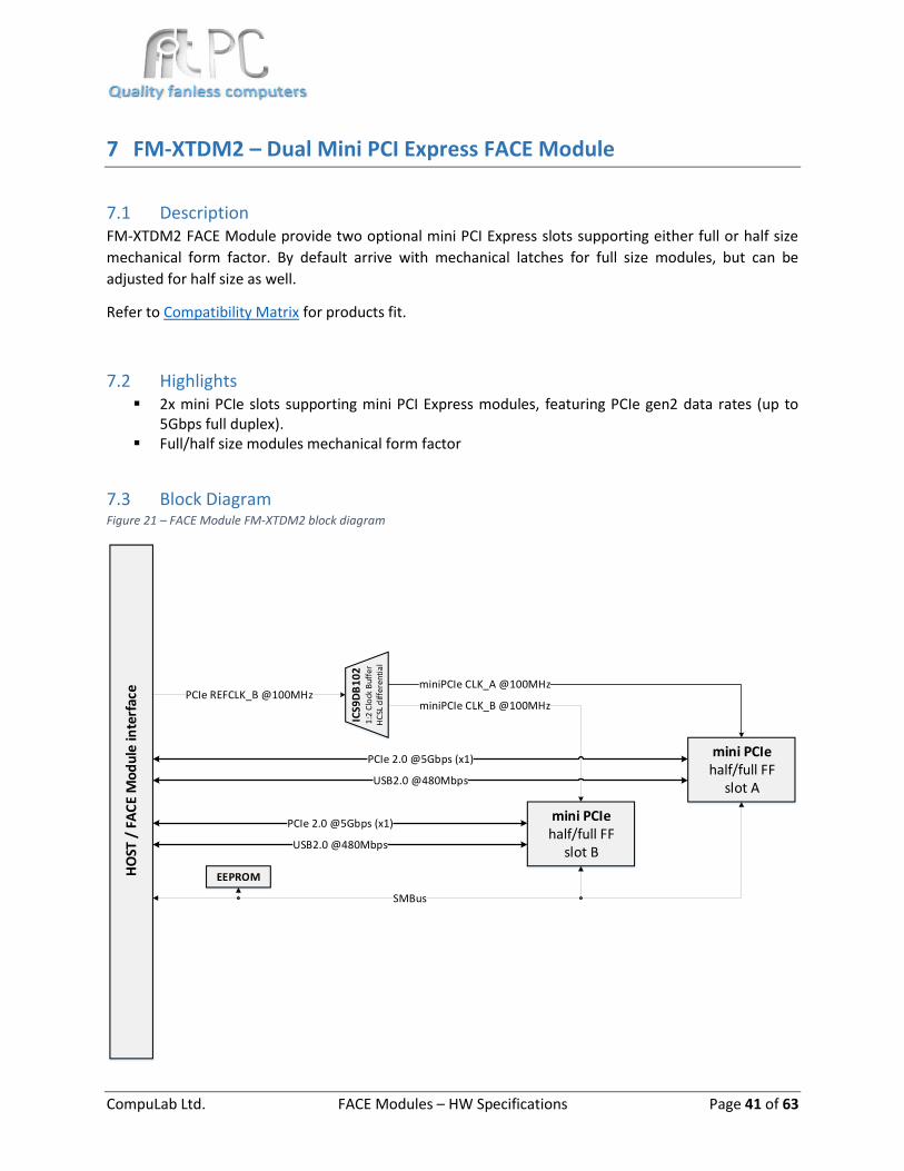
7 FM-XTDM2 – Dual Mini PCI Express FACE Module ........................................................................... 41
7.1 Description .................................................................................................................................. 41
7.2 Highlights .................................................................................................................................... 41
7.3 Block Diagram ............................................................................................................................. 41
7.4 Hardware Specifications ............................................................................................................. 42
7.4.1 Mini PCI Express Slot ............................................................................................................... 42
7.5 Mechanics ................................................................................................................................... 43
7.5.1 PCB Assembly .......................................................................................................................... 43
7.5.2 Front Panel .............................................................................................................................. 43
8 FM-VC – Video Capture FACE Module ............................................................................................... 44
8.1 Description .................................................................................................................................. 44
8.2 Highlights .................................................................................................................................... 44
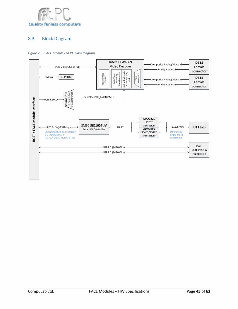
8.3 Block Diagram ............................................................................................................................. 45
8.4 Hardware Specifications ............................................................................................................. 46
8.4.1 Intersil TW6869 Video Decoder .............................................................................................. 46
8.4.2 SMSC SIO1007 Super-IO Controller ........................................................................................ 48
8.4.3 IDT ICS9DB102 1-to-2 Differential Clock Driver ...................................................................... 49
8.4.4 MAX3221 RS232 Transceiver .................................................................................................. 49
8.4.5 ADM3491 RS422/RS485 Transceiver ...................................................................................... 49
8.4.6 DB15 Connectors Pinout ......................................................................................................... 49
8.4.7 RJ11 Connector Pinout ............................................................................................................ 50
8.5 Cables .......................................................................................................................................... 51
8.5.1 DB15 to RCA and BNC Cables .................................................................................................. 51
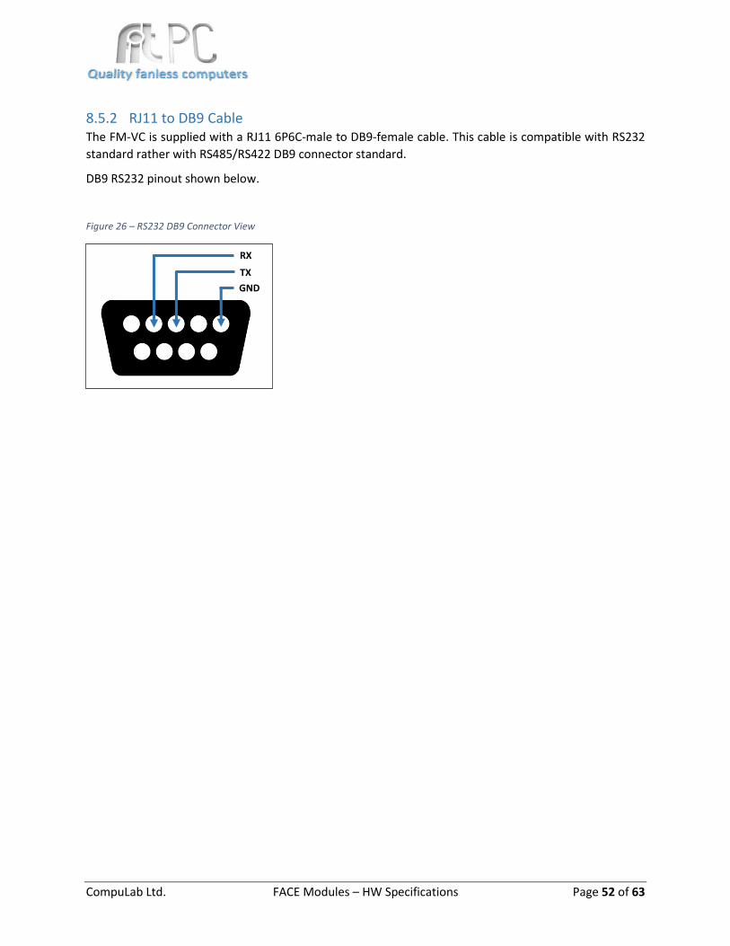
8.5.2 RJ11 to DB9 Cable ................................................................................................................... 52
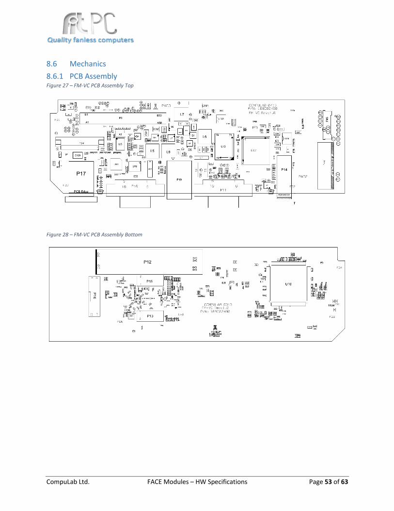
8.6 Mechanics ................................................................................................................................... 53
8.6.1 PCB Assembly .......................................................................................................................... 53
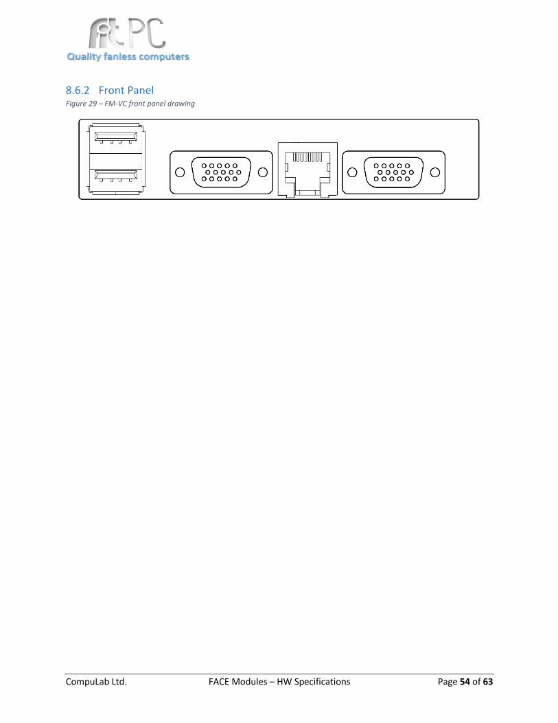
8.6.2 Front Panel .............................................................................................................................. 54

CompuLab Ltd. FACE Modules – HW Specifications Page 7 of 63
8.7 Software Drivers ......................................................................................................................... 55
9 FM-POE – Quad LAN with Power over Ethernet PSE ports ............................................................... 56
9.1 Description .................................................................................................................................. 56
9.2 Highlights .................................................................................................................................... 56
9.3 Block Diagram ............................................................................................................................. 56
9.4 Hardware Specifications ............................................................................................................. 57
9.4.1 Intel I211AT GbE Controller .................................................................................................... 57
9.4.2 Silicon Labs Si3452 Quad High Voltage Port Controller for PoE + PSE .................................... 58
9.4.3 Pericom PI6C20400 1-to-4 Differential Clock Driver ............................................................... 59
9.4.4 SPI NOR Flash .......................................................................................................................... 59
9.4.5 RJ45 PoE/PSE port pinout ....................................................................................................... 60
9.5 Mechanics ................................................................................................................................... 61
9.5.1 PCB Assembly .......................................................................................................................... 61
9.5.2 Front Panel .............................................................................................................................. 61
9.6 Software Drivers ......................................................................................................................... 62
9.7 Safety Information ...................................................................................................................... 62
10 Reference ........................................................................................................................................ 63
CompuLab Ltd. FACE Modules – HW Specifications Page 8 of 63
Table of Figures Figure 1 – FACE Module concept ................................................................................................................ 10
Figure 2 – Intense PC main board Bottom view (B2B connectors - P58, P59) ............................................ 16
Figure 3 – B2B connector footprint view (note for 180deg offset between the connectors) .................... 16
Figure 4 – FACE Module FM-4USB block diagram ...................................................................................... 18
Figure 5 – FM-4USB PCB Assembly Top ...................................................................................................... 19
Figure 6 – FM-4USB front panel drawing .................................................................................................... 19
Figure 7 – FACE Module FM-USB3 block diagram ...................................................................................... 20
Figure 8 – FM-USB3 PCB Assembly Top ...................................................................................................... 22
Figure 9 – FM-USB3 front panel .................................................................................................................. 22
Figure 10 – FACE Module FM-SER block diagram ....................................................................................... 25
Figure 11 – PLX OXPCIe958 functional block diagram ................................................................................ 26
Figure 12 – Jumper E1 location ................................................................................................................... 29
Figure 13 – FM-SER PCB Assembly Top ....................................................................................................... 30
Figure 14 – FM-SER front panel drawing .................................................................................................... 30
Figure 15 – FACE Module FM-XTDEU2/4 block diagram ............................................................................ 32
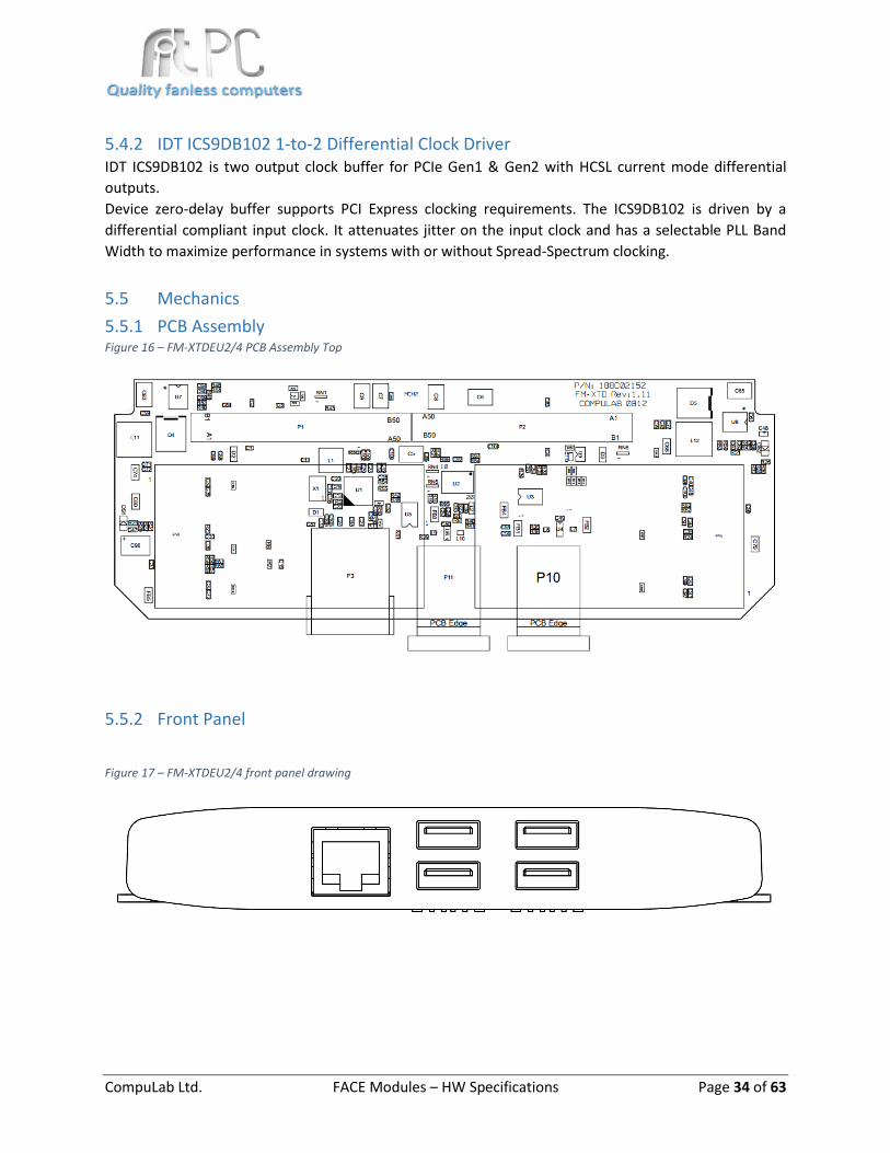
Figure 16 – FM-XTDEU2/4 PCB Assembly Top ............................................................................................ 34
Figure 17 – FM-XTDEU2/4 front panel drawing .......................................................................................... 34
Figure 18 – FACE Module FM-XTDE4U2/4 block diagram .......................................................................... 36
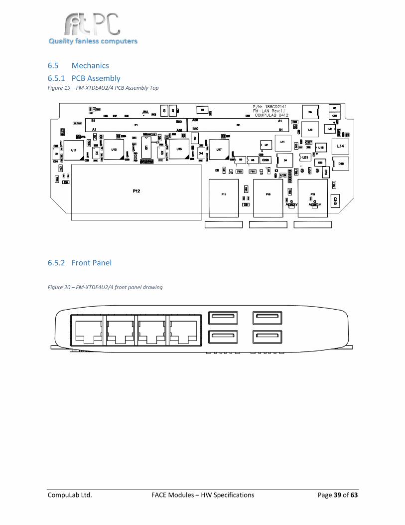
Figure 19 – FM-XTDE4U2/4 PCB Assembly Top .......................................................................................... 39
Figure 20 – FM-XTDE4U2/4 front panel drawing ........................................................................................ 39
Figure 21 – FACE Module FM-XTDM2 block diagram ................................................................................. 41
Figure 22 – FM-XTDM2 PCB Assembly Top ................................................................................................. 43
Figure 23 – FACE Module FM-VC block diagram ........................................................................................ 45
Figure 24 – Intersil TW6869 functional block diagram ............................................................................... 47
Figure 25 – SMSC SIO1007 functional block diagram ................................................................................. 48
Figure 26 – RS232 DB9 Connector View ..................................................................................................... 52
Figure 27 – FM-VC PCB Assembly Top ........................................................................................................ 53
Figure 28 – FM-VC PCB Assembly Bottom .................................................................................................. 53
Figure 29 – FM-VC front panel drawing ...................................................................................................... 54
Figure 30 – FACE Module FM-POE block diagram ...................................................................................... 56
Figure 31 – Silicon Labs Si3452 functional block diagram .......................................................................... 58
Figure 32 – RJ45 Jack drawing ..................................................................................................................... 60
Figure 33 – FM-POE PCB Assembly Top ...................................................................................................... 61
Figure 34 – FM-POE front panel drawing .................................................................................................... 61
Table of Tables Table 1 – B2B receptacle connector HOST side .......................................................................................... 11
Table 2 – B2B plug connector FACE Module side ....................................................................................... 11
Table 3 – EXT1 connector HOST side pinout ............................................................................................... 12
Table 4 – EXT2 connector HOST side pinout ............................................................................................... 14
CompuLab Ltd. FACE Modules – HW Specifications Page 9 of 63
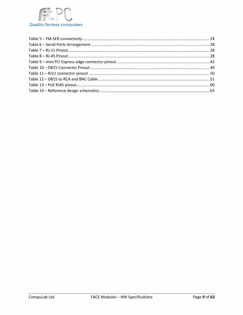
Table 5 – FM-SER connectivity .................................................................................................................... 24
Table 6 – Serial Ports Arrangement ............................................................................................................ 28
Table 7 – RJ-11 Pinout ................................................................................................................................. 28
Table 8 – RJ-45 Pinout ................................................................................................................................. 28
Table 9 – mini PCI Express edge connector pinout ..................................................................................... 42
Table 10 – DB15 Connector Pinout ............................................................................................................. 49
Table 11 – RJ11 connector pinout .............................................................................................................. 50
Table 12 – DB15 to RCA and BNC Cable ...................................................................................................... 51
Table 13 – PoE RJ45 pinout ......................................................................................................................... 60
Table 14 – Reference design schematics .................................................................................................... 63
CompuLab Ltd. FACE Modules – HW Specifications Page 10 of 63
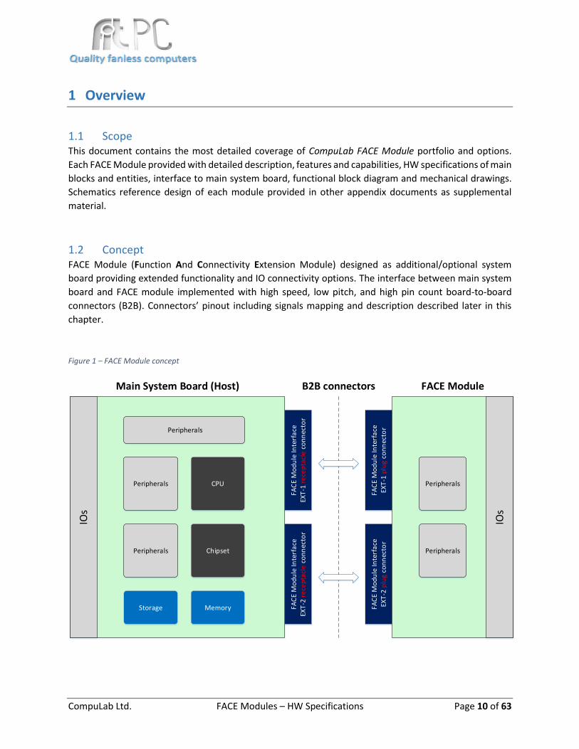
1 Overview
1.1 Scope This document contains the most detailed coverage of CompuLab FACE Module portfolio and options.
Each FACE Module provided with detailed description, features and capabilities, HW specifications of main
blocks and entities, interface to main system board, functional block diagram and mechanical drawings.
Schematics reference design of each module provided in other appendix documents as supplemental
material.
1.2 Concept FACE Module (Function And Connectivity Extension Module) designed as additional/optional system
board providing extended functionality and IO connectivity options. The interface between main system
board and FACE module implemented with high speed, low pitch, and high pin count board-to-board
connectors (B2B). Connectors’ pinout including signals mapping and description described later in this
chapter.
Figure 1 – FACE Module concept
FAC
E M
od
ule
Inte
rfa
ceEX
T-2
plu
g co
nn
ecto
rFA
CE
Mo
du
le In
terf
ace
EXT
-1 p
lug
con
nec
tor
FAC
E M
od
ule
Inte
rfa
ceEX
T-2
re
cep
tacl
e c
on
nec
tor
FAC
E M
od
ule
Inte
rfa
ceEX
T-1
re
cep
tacl
e c
on
nec
tor
Peripherals
Peripherals
CPU
Chipset
IOs
Peripherals
Peripherals
Main System Board (Host) FACE Module
IOs
B2B connectors
MemoryStorage
Peripherals
CompuLab Ltd. FACE Modules – HW Specifications Page 11 of 63
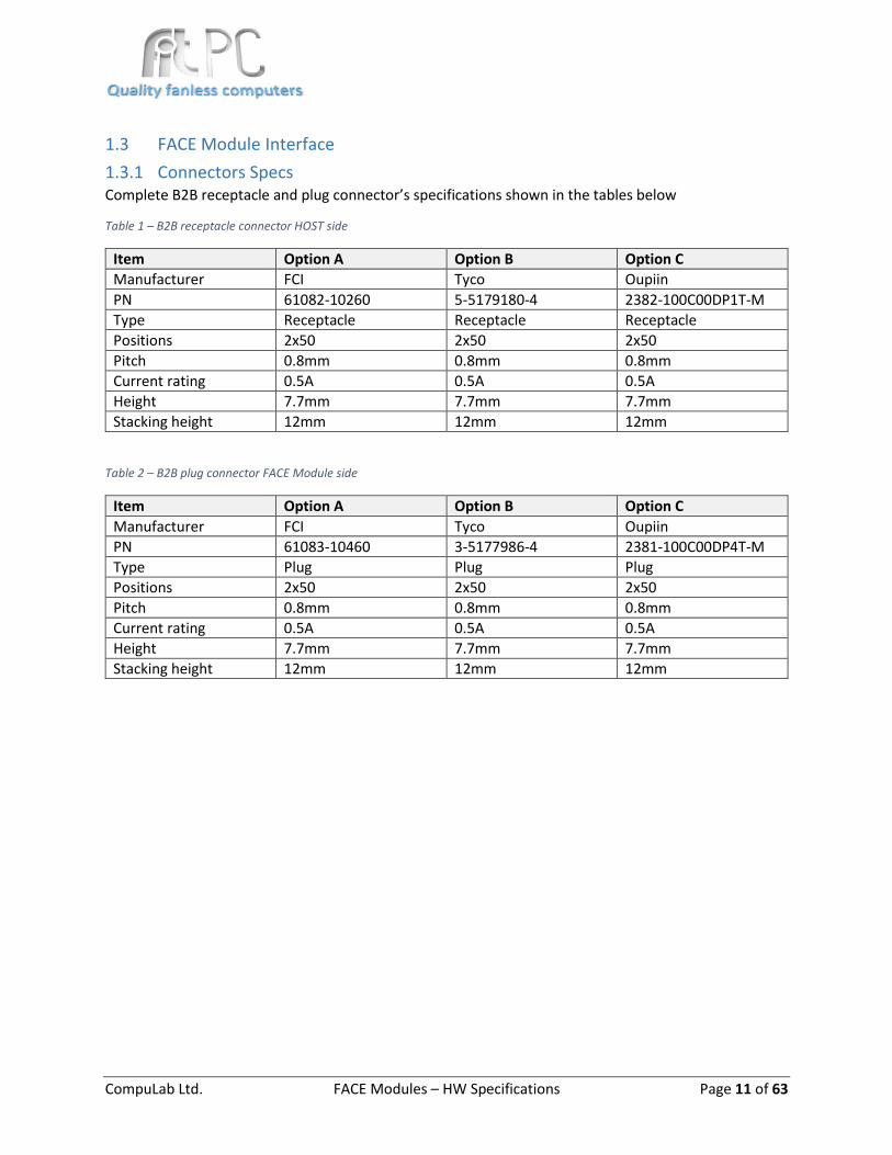
1.3 FACE Module Interface
1.3.1 Connectors Specs Complete B2B receptacle and plug connector’s specifications shown in the tables below
Table 1 – B2B receptacle connector HOST side
Item Option A Option B Option C
Manufacturer FCI Tyco Oupiin
PN 61082-10260 5-5179180-4 2382-100C00DP1T-M
Type Receptacle Receptacle Receptacle
Positions 2x50 2x50 2x50
Pitch 0.8mm 0.8mm 0.8mm
Current rating 0.5A 0.5A 0.5A
Height 7.7mm 7.7mm 7.7mm
Stacking height 12mm 12mm 12mm
Table 2 – B2B plug connector FACE Module side
Item Option A Option B Option C
Manufacturer FCI Tyco Oupiin
PN 61083-10460 3-5177986-4 2381-100C00DP4T-M
Type Plug Plug Plug
Positions 2x50 2x50 2x50
Pitch 0.8mm 0.8mm 0.8mm
Current rating 0.5A 0.5A 0.5A
Height 7.7mm 7.7mm 7.7mm
Stacking height 12mm 12mm 12mm

CompuLab Ltd. FACE Modules – HW Specifications Page 12 of 63
1.3.2 Connectors Pinout The tables below provide complete pinout of extension connectors EXT1, EXT2 and signals mapping.
Table 3 – EXT1 connector HOST side pinout
EXT-1 connector HOST side
Pin # Pin Name Signal Description Pin # Pin Name Signal Description
A1 GND Ground connection B1 GND Ground connection
A2 SATA2_TX+ SATA2.0 differential transmit pair 2; Host signal shared with mini PCIe (MUX channel B)
B2 SATA0_TX+/CLK+ Host PEG CLK output differential pair - 100MHz PCIe Gen2 to PCIe Graphics device1 A3 SATA2_TX- B3 SATA0_TX-/CLK-
A4 IR_RX IR UART receive signal B4 SATA0_LED SATA activity LED indicator
A5 SATA2_RX+ SATA2.0 differential receive pair 2; Host signal shared with mini PCIe (MUX channel B) 3
B5 SATA0_RX+/CLK+ Host PCIe CLK output differential pair - 100MHz PCIe Gen2 to PCIe devices1 A6 SATA2_RX- B6 SATA0_RX-/CLK-
A7 GND Ground connection B7 V5SBY 5V power domain
A8 SATA3_TX+
SATA2.0 differential transmit pair 33
B8 SATA1_RX+
SATA3.0 differential receive pair 12 A9 SATA3_TX- B9 SATA1_RX-
A10 SMB_ALRT# SMBus Alert used to wake the system B10 DEBUG1 Reserved debug signal
A11 SATA3_RX+
SATA2.0 differential receive pair 33
B11 SATA1_TX+
SATA3.0 differential transmit pair 12 A12 SATA3_RX- B12 SATA1_TX-
A13 V5SBY 5V power domain B13 V5SBY 5V power domain
A14 SMB_CLK SMBus host clock output. Connect to SMBus slave. B14 USB3_P
USB Host interface 3 A15 SMB_DAT SMBus bidirectional data. Connect to SMBus slave. B15 USB3_N
A16 HDA_RST# High Definition Audio host reset B16 USB_OC_2_3# USB Overcurrent Indicator for lanes 2/3
A17 HDA_SYNC High Definition Audio host sync B17 USB2_P
USB Host interface 2 A18 HDA_BITCLK High Definition Audio host bit clock out 24MHz B18 USB2_N
A19 HDA_SDOUT High Definition Audio serial host data out B19 V5SBY 5V power domain
A20 HDA_SDIN1 High Definition Audio serial host data in1 B20 COM2_RX For internal test purposes
A21 HDA_SDIN0 High Definition Audio serial host data in0 B21 COM2_TX For internal test purposes
A22 DEBUG3 Reserved debug signal B22 LPC_SERIRQ Serial Interrupt Request
A23 GND Ground connection B23 LPC_CLK Single Ended 33MHz CLK host out to PCI devices
A24 USB0_P
USB Host interface lane 0
B24 LPC_FRAME# LPC interface frame signal
A25 USB0_N B25 GND Ground connection
A26 USB_OC0_1# USB Overcurrent Indicator for lanes 0/1 B26 SPI_MISO SPI interface MISO signal – Reserved for internal use only
A27 USB1_P
USB Host interface 1
B27 SPI_MOSI SPI interface MOSI signal – Reserved for internal use only
A28 USB1_N B28 SPI_CLK SPI interface Clock signal – Reserved for internal use only
A29 GND Ground connection B29 SPI_CS1# SPI interface chip select 1 – Reserved for internal use only
A30 LPC_AD0
LPC bus multiplexed command, address and data. Internal PU provided on LPC[3:0]
B30 SPI_CS0# SPI interface chip select 0 – Reserved for internal use only
A31 LPC_AD1 B31 RESET# Active Low Platform Reset driven by the Host
A32 LPC_AD2 B32 PCIE_CLK+ Host PCIe CLK output differential pair - 100MHz PCIe Gen2 to PCIe devices A33 LPC_AD3 B33 PCIE_CLK-
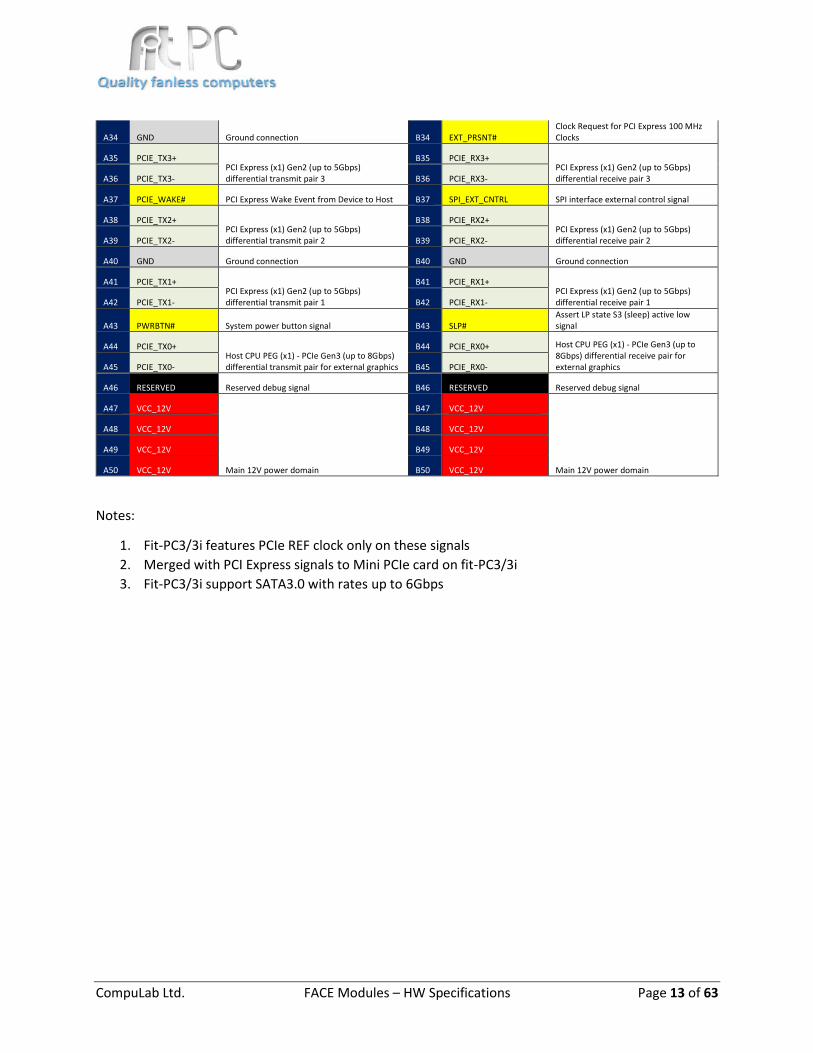
CompuLab Ltd. FACE Modules – HW Specifications Page 13 of 63
A34 GND Ground connection B34 EXT_PRSNT# Clock Request for PCI Express 100 MHz Clocks
A35 PCIE_TX3+ PCI Express (x1) Gen2 (up to 5Gbps) differential transmit pair 3
B35 PCIE_RX3+ PCI Express (x1) Gen2 (up to 5Gbps) differential receive pair 3 A36 PCIE_TX3- B36 PCIE_RX3-
A37 PCIE_WAKE# PCI Express Wake Event from Device to Host B37 SPI_EXT_CNTRL SPI interface external control signal
A38 PCIE_TX2+ PCI Express (x1) Gen2 (up to 5Gbps) differential transmit pair 2
B38 PCIE_RX2+ PCI Express (x1) Gen2 (up to 5Gbps) differential receive pair 2 A39 PCIE_TX2- B39 PCIE_RX2-
A40 GND Ground connection B40 GND Ground connection
A41 PCIE_TX1+ PCI Express (x1) Gen2 (up to 5Gbps) differential transmit pair 1
B41 PCIE_RX1+ PCI Express (x1) Gen2 (up to 5Gbps) differential receive pair 1 A42 PCIE_TX1- B42 PCIE_RX1-
A43 PWRBTN# System power button signal B43 SLP# Assert LP state S3 (sleep) active low signal
A44 PCIE_TX0+ Host CPU PEG (x1) - PCIe Gen3 (up to 8Gbps) differential transmit pair for external graphics
B44 PCIE_RX0+ Host CPU PEG (x1) - PCIe Gen3 (up to 8Gbps) differential receive pair for external graphics A45 PCIE_TX0- B45 PCIE_RX0-
A46 RESERVED Reserved debug signal B46 RESERVED Reserved debug signal
A47 VCC_12V
Main 12V power domain
B47 VCC_12V
Main 12V power domain
A48 VCC_12V B48 VCC_12V
A49 VCC_12V B49 VCC_12V
A50 VCC_12V B50 VCC_12V
Notes:
1. Fit-PC3/3i features PCIe REF clock only on these signals
2. Merged with PCI Express signals to Mini PCIe card on fit-PC3/3i
3. Fit-PC3/3i support SATA3.0 with rates up to 6Gbps

CompuLab Ltd. FACE Modules – HW Specifications Page 14 of 63
Table 4 – EXT2 connector HOST side pinout
EXT-2 connector HOST side
Pin # Pin Name Signal Description Pin # Pin Name Signal Description
A1 GND Ground connection B1 GND Ground connection
A2 PEG_RX0+/RSVD0 Host CPU PEG_0 (x8) - PCIe Gen3 (up to 8Gbps) differential receive pair for external graphics 1
B2 PEG_TX0+/RSVD6 Host CPU PEG_0 (x8) - PCIe Gen3 (up to 8Gbps) differential transmit pair for external graphics 1 A3 PEG_RX0-/RSVD1 B3 PEG_TX0-/RSVD7
A4 DGPU_PRSNT#/RSVD3 Host chipset GPIO67, Input, PU-10k B4 DGPU_PWREN#/RSVD8 Host chipset GPIO54, Output, PU-8.2k
A5 PEG_RX1+/RSVD4 Host CPU PEG_1 (x8) - PCIe Gen3 (up to 8Gbps) differential receive pair for external graphics 1
B5 PEG_TX1+/RSVD9 Host CPU PEG_1 (x8) - PCIe Gen3 (up to 8Gbps) differential transmit pair for external graphics 1 A6 PEG_RX1-/RSVD5 B6 PEG_TX1-/RSVD10
A7 GND Ground connection B7 GND Ground connection
A8 PEG_RX2+/RSVD11 Host CPU PEG_2 (x8) - PCIe Gen3 (up to
8Gbps) differential receive pair for external graphics 2
B8 PEG_TX2+/RSVD16 Host CPU PEG_2 (x8) - PCIe Gen3 (up to 8Gbps) differential transmit pair for external graphics 2 A9
PEG_RX2-/RSVD12 B9 PEG_TX2-/RSVD17
A10 DGPU_PWROK/RSVD13 Host chipset GPIO17, Input/Output, PD-10k B10
DGPU_HOLD_RST#/RSVD18 Host chipset GPIO50, Output, PU-8.2k
A11 PEG_RX3+/RSVD14 Host CPU PEG_3 (x8) - PCIe Gen3 (up to
8Gbps) differential receive pair for external graphics 2
B11 PEG_TX3+/RSVD19 Host CPU PEG_3 (x8) - PCIe Gen3 (up to 8Gbps) differential transmit pair for external graphics 2 A12
PEG_RX3-/RSVD15 B12 PEG_TX3-/RSVD20
A13 GND Ground connection B13 GND Ground connection
A14 PEG_RX4+/RSVD21 Host CPU PEG_4 (x8) - PCIe Gen3 (up to
8Gbps) differential receive pair for external graphics 2
B14 PEG_TX4+/RSVD26 Host CPU PEG_4 (x8) - PCIe Gen3 (up to 8Gbps) differential transmit pair for external graphics 2 A15
PEG_RX4-/RSVD22 B15 PEG_TX4-/RSVD27
A16 DGPU_SELECT#/RSVD23 Host chipset GPIO52, Output, PU-8.2k B16
DGPU_HPD_INTR#/RSVD28 Host chipset GPIO6, Input, PU-10k
A17 PEG_RX5+/RSVD24 Host CPU PEG_5 (x8) - PCIe Gen3 (up to
8Gbps) differential receive pair for external graphics 2
B17 PEG_TX5+/RSVD29 Host CPU PEG_5 (x8) - PCIe Gen3 (up to 8Gbps) differential transmit pair for external graphics 2 A18
PEG_RX5-/RSVD25 B18 PEG_TX5-/RSVD30
A19 V5SBY 5V power domain B19 V5SBY 5V power domain
A20 PEG_RX6+/RSVD31 Host CPU PEG_6 (x8) - PCIe Gen3 (up to
8Gbps) differential receive pair for external graphics 2
B20 PEG_TX6+/RSVD36 Host CPU PEG_6 (x8) - PCIe Gen3 (up to 8Gbps) differential transmit pair for external graphics 2 A21
PEG_RX6-/RSVD32 B21 PEG_TX6-/RSVD37
A22 DGPU_PWM_SELECT#/RSVD33 Host chipset GPIO53, Output, No pull B22 SPARE/eDP_HDP NC
A23 PEG_RX7+/RSVD34 Host CPU PEG_7 (x8) - PCIe Gen3 (up to
8Gbps) differential receive pair for external graphics 2
B23 PEG_TX7+/RSVD38 Host CPU PEG_7 (x8) - PCIe Gen3 (up to 8Gbps) differential transmit pair for external graphics 2 A24
PEG_RX7-/RSVD35 B24 PEG_TX7-/RSVD39
A25 GND Ground connection B25 GND Ground connection
A26 LVDS_A0+/eDP_TX0+
LVDS Channel A differential pair 0 Host data output 3
B26 PEG_CLK+/RSVD40 Host PEG CLK output differential pair - 100MHz PCIe Gen2 to PCIe Graphics device A27
LVDS_A0-/eDP_TX0- B27 PEG_CLK-/RSVD41
A28 LVDS_A1+/eDP_TX1+
LVDS Channel A differential pair 1 Host data output 3
B28 LVDS_BKLT_CTRL Panel Backlight Brightness Control 3
A29 LVDS_A1-/eDP_TX1- B29 COM1_DCR
Full RS232 interface from Host to DCE device
A30 LVDS_A2+/eDP_TX2+
LVDS Channel A differential pair 2 Host data output 3
B30 COM1_TX
A31 LVDS_A2-/eDP_TX2- B31 COM1_DCD
A32 GND Ground connection B32 GND Ground connection

CompuLab Ltd. FACE Modules – HW Specifications Page 15 of 63
A33 LVDS_A3+/eDP_TX3+
LVDS Channel A differential pair 3 Host data output 3
B33 COM1_DTR
Full RS232 interface from Host to DCE device
A34 LVDS_A3-/eDP_TX3- B34 COM1_RTS
A35 LVDS_VDD_EN LVDS Panel Power Enable 3 B35 COM1_RX
A36 LVDS_ACLK+/eDP_AUX+
LVDS Channel A differential pair Host clock output 3
B36 COM1_CTS
A37 LVDS_ACLK-/eDP_AUX- B37 COM1_RI
A38 GND Ground connection B38 LVDS_BKLT_EN LVDS Backlight Enable 3
A39 LVDS_CTRL_CLK LVDS Control interface for external SSC clock chip (I2C based). Optional. 3
B39 LVDS_I2C_CLK LVDS DDC (I2C based) management interface. EDID support for flat panel display 3 A40 LVDS_CTRL_DATA B40 LVDS_I2C_DAT
A41 PEG_CLK_REQ#/RSVD42 Clock Request Signal for PCIe Graphics (PEG) B41 GND Ground connection
A42 RESERVED
Reserved
B42 RESERVED
Reserved A43 RESERVED B43 RESERVED
A44 GND Ground connection B44 NC NC
A45 RESERVED
Reserved
B45 RESERVED
Reserved A46 RESERVED B46 RESERVED
A47 USB_OC_4_5# USB Overcurrent Indicator for lanes 2/3 B47 SPARE0 Host chipset spare GPIO
A48 USB4_P
USB Host interface 4
B48 VCC_12V
Main 12V power domain
A49 USB4_N B49 VCC_12V
A50 GND Ground connection B50 VCC_12V
Notes:
1. Merged with PCI Express signals to Mini PCIe card on fit-PC3/3i
2. GPIOs on fit-PC3/3i
3. Fit-PC3/3i design does not feature LVDS interface

CompuLab Ltd. FACE Modules – HW Specifications Page 16 of 63
1.4 Layout Host side extension connector’s footprints with respect to board geometry shown in the below layout
captures. Host side extension connectors provide complete Host/FACE Module interface connectivity.
FACE Module side may have either both or only one of the connectors, connecting only FACE Module
relevant signals.
Note for 180deg orientation offset between the connectors.
Figure 2 – Intense PC main board Bottom view (B2B connectors - P58, P59)
Figure 3 – B2B connector footprint view (note for 180deg offset between the connectors)
CompuLab Ltd. FACE Modules – HW Specifications Page 17 of 63
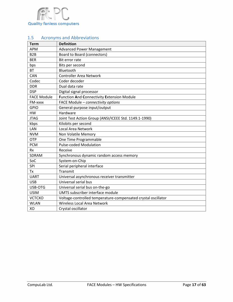
1.5 Acronyms and Abbreviations Term Definition
APM Advanced Power Management
B2B Board to Board (connectors)
BER Bit error rate
bps Bits per second
BT Bluetooth
CAN Controller Area Network
Codec Coder decoder
DDR Dual data rate
DSP Digital signal processor
FACE Module Function And Connectivity Extension Module
FM-xxxx FACE Module – connectivity options
GPIO General-purpose input/output
HW Hardware
JTAG Joint Test Action Group (ANSI/ICEEE Std. 1149.1-1990)
kbps Kilobits per second
LAN Local Area Network
NVM Non Volatile Memory
OTP One Time Programmable
PCM Pulse-coded Modulation
Rx Receive
SDRAM Synchronous dynamic random access memory
SoC System-on-Chip
SPI Serial peripheral interface
Tx Transmit
UART Universal asynchronous receiver transmitter
USB Universal serial bus
USB-OTG Universal serial bus on-the-go
USIM UMTS subscriber interface module
VCTCXO Voltage-controlled temperature-compensated crystal oscillator
WLAN Wireless Local Area Network
XO Crystal oscillator

CompuLab Ltd. FACE Modules – HW Specifications Page 18 of 63
2 FM-4USB – USB2.0 FACE Module
2.1 Description FM-4USB is the basic FACE Module provide 4x USB2.0 (up to 480Mbps) extended connectivity. Used as
default option in CompuLab system configurations.
Refer to Compatibility Matrix for products fit.
2.2 Highlights 4x USB2.0 downstream ports, up to 480Mbps half-duplex
2.3 Block Diagram Figure 4 – FACE Module FM-4USB block diagram
USB Type-A receptacle
USB Type-A receptacle
USB Type-A receptacle
USB Type-A receptacle
HO
ST /
FA
CE
Mo
du
le in
terf
ace
(EX
T1 c
on
ne
cto
r o
nly
)
USB2.0 @480Mbps
USB2.0 @480Mbps
USB2.0 @480Mbps
USB2.0 @480Mbps
USB VBUS current limitCommon Mode noise filtering
ESD protection

CompuLab Ltd. FACE Modules – HW Specifications Page 19 of 63
2.4 Mechanics
2.4.1 PCB Assembly Figure 5 – FM-4USB PCB Assembly Top
2.4.2 Front Panel
Figure 6 – FM-4USB front panel drawing

CompuLab Ltd. FACE Modules – HW Specifications Page 20 of 63
3 FM-USB3 – USB3.0 FACE Module
3.1 Description FM-USB3 FACE Module provide market new USB3.0 Super Speed connectivity, with legacy USB2.0
downstream ports. In addition single mSATA SSD storage card can be implemented via mini PCIe slot
either half or full form factors.
Compatible with IPC2 computers only.
Refer to Compatibility Matrix for products fit.
3.2 Highlights 2x USB3.0 downstream ports (USB2.0 supported on separate pins), up to 5Gbps full-duplex
1x mSATA slot allow to connect mSATA SSD storage (on IPC2 i5/i7 models only)
3.3 Block Diagram
Figure 7 – FACE Module FM-USB3 block diagram
HO
ST /
FA
CE
Mo
du
le in
terf
ace
EEPROMSMBus
USB3 Type-A Receptacle
USB3 Type-A Receptacle
USB2.0
USB3.0_TXUSB3.0_RX
USB2.0
USB3.0_TXUSB3.0_RX
SATA3.0/PCIe2.0 mSATA slotfull/half FFPCIe REFCLK @100MHz
ON/OFFStorage activity
Sleep
LED Indications
CompuLab Ltd. FACE Modules – HW Specifications Page 21 of 63
3.4 Hardware Specifications The following section provides information about FM-USB3 main components and features.
3.4.1 mSATA slot FM-USB3 incorporates single mSATA slot (i5/i7 models only) and provides an option for connecting
either full or half size form factor card.
CompuLab Ltd. FACE Modules – HW Specifications Page 22 of 63
3.5 Mechanics
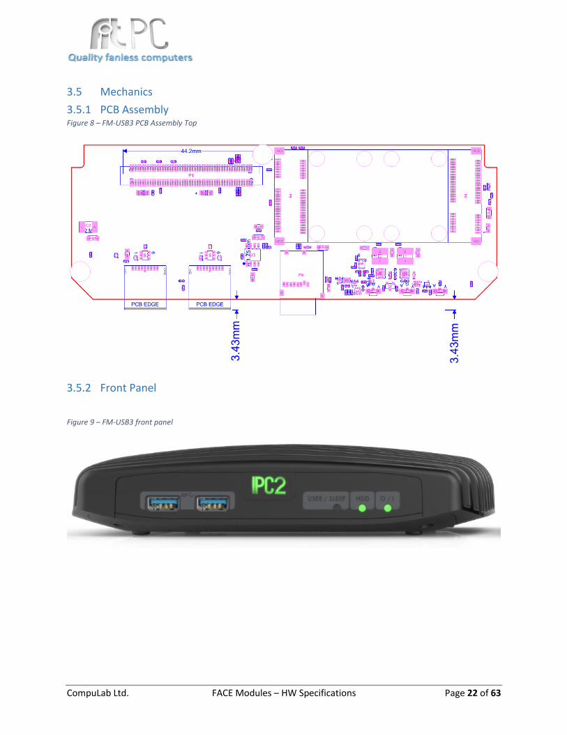
3.5.1 PCB Assembly Figure 8 – FM-USB3 PCB Assembly Top
3.5.2 Front Panel
Figure 9 – FM-USB3 front panel
CompuLab Ltd. FACE Modules – HW Specifications Page 23 of 63
3.6 Software Drivers
Windows Drivers
— Not required, except IPC2 chipset driver as USB3.0 ports are IPC2 chipset native
Linux Drivers
— Implemented in Linux Kernel (same as above)
CompuLab Ltd. FACE Modules – HW Specifications Page 24 of 63
4 FM-SER – Serial FACE Module
4.1 Description FM-SER FACE Module provide various serial connectivity solution and compatible with several Compulab
systems.
Refer to Compatibility Matrix for products fit.
4.2 Highlights High performance UARTS
Asynchronous baud rates up to 15Mbps
128-byte deep TX/RX FIFOs
Advanced FIFO fill management
RS232, RS485, RS422 operation
Programmable RS485 turn-around delay
450 through 950 software compatibility
Two independent CAN bus controllers implement CAN V2.0B at rate of up to 1Mbps each
Isolated PHY with rated isolation voltage of 2.5 kV RMS
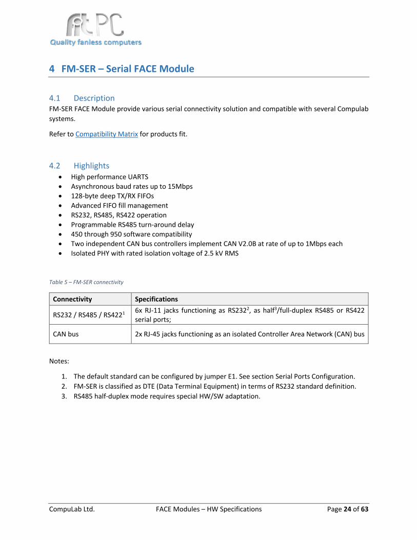
Table 5 – FM-SER connectivity
Connectivity Specifications
RS232 / RS485 / RS4221 6x RJ-11 jacks functioning as RS2322, as half3/full-duplex RS485 or RS422 serial ports;
CAN bus 2x RJ-45 jacks functioning as an isolated Controller Area Network (CAN) bus
Notes:
1. The default standard can be configured by jumper E1. See section Serial Ports Configuration.
2. FM-SER is classified as DTE (Data Terminal Equipment) in terms of RS232 standard definition.
3. RS485 half-duplex mode requires special HW/SW adaptation.

CompuLab Ltd. FACE Modules – HW Specifications Page 25 of 63
4.3 Block Diagram
Figure 10 – FACE Module FM-SER block diagram
HO
ST /
FA
CE
Mo
du
le in
terf
ace
USB2.0 @480Mbps
USB2.0 @480Mbps
PCIe 1.1 @2.5Gbps (x1)
PCA9555GPIO Controller
PLX OXPCIe9588x UART
ControllerPCIe REFCLK @100MHz
Dual RJ45 Jack
3x LTC2872 Dual
RS232/RS485MultimodeTransceiver
Dual RJ11 Jack
FTDI FT232HUSB to UART/SPI
Bridge
FTDI FT232HUSB to UART/SPI
Bridge
MCP2515 CAN
Controller
MCP2515 CAN
Controller
EEPROM
SMBus
SPI
SPI
ADM3053 Isolated
CAN driver
ADM3053 Isolated
CAN driver
RS232/RS485
RS232/RS485
Dual RJ11 Jack
Dual RJ11 Jack
RS232/RS485
RS232/RS485
RS232/RS485
RS232/RS485
UART
UART
UART
UART
UART
UART
CANiso
CANiso
CAN
CAN
16x Control GPIOs
EEPROM SPI
EEPROM
EEPROM
PCIE_WAKE_UP#
SYS_RESET
CompuLab Ltd. FACE Modules – HW Specifications Page 26 of 63
4.4 Hardware Specifications The following section provides information about the main components and respective features, as well
as available configuration options.
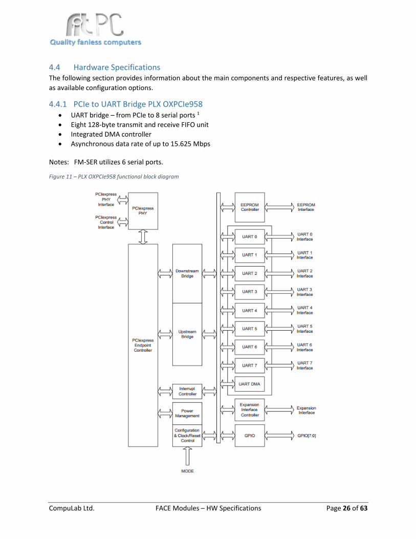
4.4.1 PCIe to UART Bridge PLX OXPCIe958 UART bridge – from PCIe to 8 serial ports 1
Eight 128-byte transmit and receive FIFO unit
Integrated DMA controller
Asynchronous data rate of up to 15.625 Mbps
Notes: FM-SER utilizes 6 serial ports.
Figure 11 – PLX OXPCIe958 functional block diagram

CompuLab Ltd. FACE Modules – HW Specifications Page 27 of 63
4.4.2 LTC2872 Dual Multiprotocol Transceiver Three dual transceivers are onboard the FM-SER provide 6 multiprotocol serial ports.
Implementation of physical layer (PHY) of RS232 or RS485 serial protocol ports. See section 4.1: Serial Ports Configuration.
Up to 500kbps data rate from UART to RS232 and up to 15 Mbps data rate to full duplex RS485
Supports RS422 and half duplex RS485 protocols
Integrated termination resistors are being switched according to mode of operation.
Loopback mode for self-testing
4.4.3 CAN Bus Controller MCP2515 Connected to SPI bus originated from a USB to SPI bridge
Two CAN bus controllers implement CAN V2.0B at rate of up to 1Mbps each.
Six 29-bit filters, two 29-bit masks and two receive buffers with prioritized message storage
Interrupt outputs from CAN bus controllers and a shared reset input are connected to the host motherboard.
4.4.4 CAN PHY ADM3053 (Isolation Driver) Isolated physical layer (PHY) transceiver with rated isolation voltage of 2.5 kV RMS for 1 minute
Data rate of up to 1Mbps
Consumers power from the CAN bus by default, and can be configured to supply power of up to 170 mA to the bus.

CompuLab Ltd. FACE Modules – HW Specifications Page 28 of 63
4.4.5 RJ-11 Serial Ports The serial ports are arranged as COM ports differently on different motherboard configurations, as
detailed in Table 2. The physical locations of the ports are depicted in Figure 1.
Table 6 – Serial Ports Arrangement
Motherboard P1 P2 P3 P4 P5 P6
fit-PC3/ SBC-fitPC3
9 8 5 4 7 6
Intense-PC/ SBC-iSB
10 9 6 5 8 7
The pinout of RJ-11 serial ports is detailed in Table 3.
Table 7 – RJ-11 Pinout
RS232 1 RS485 2
Pin # 3 Type Functionality Type Functionality
1 O RTS O TX-
2 - GND - GND
3 O TX O TX+
4 I RX I RX+
5 - GND - GND
6 I CTS I RX-
Notes:
1. FM-SER is classified as DTE (Data Terminal Equipment) in terms of RS232 standard definition
2. FM-SER supports full duplex RS485
3. The port numbering is specified in Table 2
4.4.6 RJ-45 CAN Bus Pinout Table 8 – RJ-45 Pinout
Pin # Type Functionality
1 IO CAN +
2 IO CAN -
3 - CAN GND
4 NC NC
5 NC NC
6 - GND
7 PWR CAN GND
8 PWR CAN VCC

CompuLab Ltd. FACE Modules – HW Specifications Page 29 of 63
4.5 Configuration
4.5.1 Serial Ports Configuration Each serial port can be individually configured to act in RS232 mode or RS485 half/full duplex mode. The
configuration is selected in fit-PC3 BIOS setup.
The default selection between RS232 and RS485/RS422 is determined by E1 jumper position. Default
mode determines the power-up state of the Dual Protocol Transceiver. It is applied to all ports and
remains valid in case that software configuration is not performed.
The options of jumper E1 selections are detailed in Table 4.
Table 4 Jumper E1 options
Jumper Position 1 Default Serial Protocol
Assembled RS232
Removed RS485 / RS422
Note: The jumper is assembled by default.
Figure 12 – Jumper E1 location
After power-up, any individual port can be configured using software controlled SMBus system
management protocol.
4.5.2 CAN Bus power supply By default, the FM-SER consumes power from the CAN bus.
After power-up, the power supply option can be determined by a GPIO line connected to the motherboard,
and is fully software controlled.
CompuLab Ltd. FACE Modules – HW Specifications Page 30 of 63
P1 P2 P3 P4 P5 P6 P7 P8
4.6 Mechanics
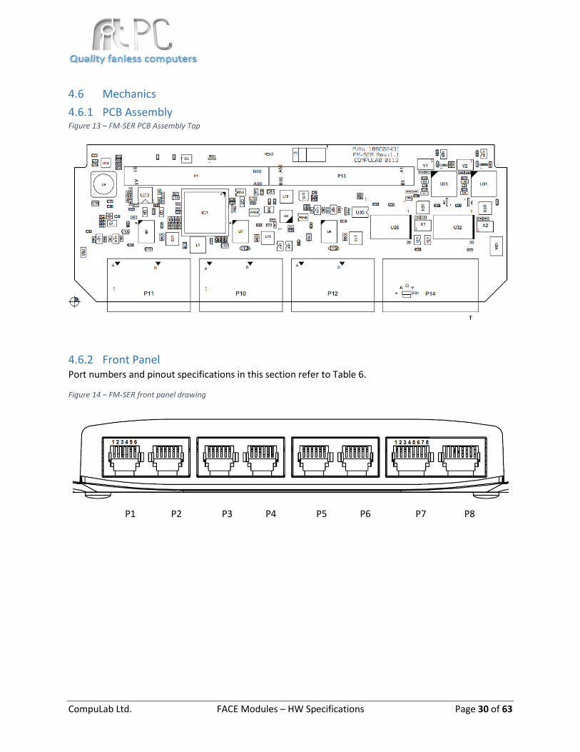
4.6.1 PCB Assembly Figure 13 – FM-SER PCB Assembly Top
4.6.2 Front Panel Port numbers and pinout specifications in this section refer to Table 6.
Figure 14 – FM-SER front panel drawing
P1 P2 P3 P4 P5 P6 P7 P8

CompuLab Ltd. FACE Modules – HW Specifications Page 31 of 63
4.7 Software Drivers The OXPCIe958 PCIe to UART Bridge and the USB to SPI Bridge must have installed driver to function
properly.
Windows Drivers
Drivers for Fit-PC / SBC-Fit-PC can be downloaded from Compulab homepage, or directly from the
following links:
— Fit-PC / SBC-Fit-PC: http://fit-pc.com/wiki/index.php/Fit-PC3:_Software#Windows_7
— Intense-PC / SBC-iSB: http://fit-pc.com/wiki/index.php/IntensePC:_Software#Windows_7
Linux Drivers
The OXPCIe958 PCIe to UART Bridge is supported by mainline kernel, and can be also found at:
https://git.kernel.org/cgit/linux/kernel/git/torvalds/linux.git/tree/drivers/tty/serial/8250/8250_pci.c?id=r
efs/tags/v3.10
Note: CAN Bus feature is yet to be supported for Linux OS.
CompuLab Ltd. FACE Modules – HW Specifications Page 32 of 63
5 FM-XTDEU2/4 – Single LAN FACE Module
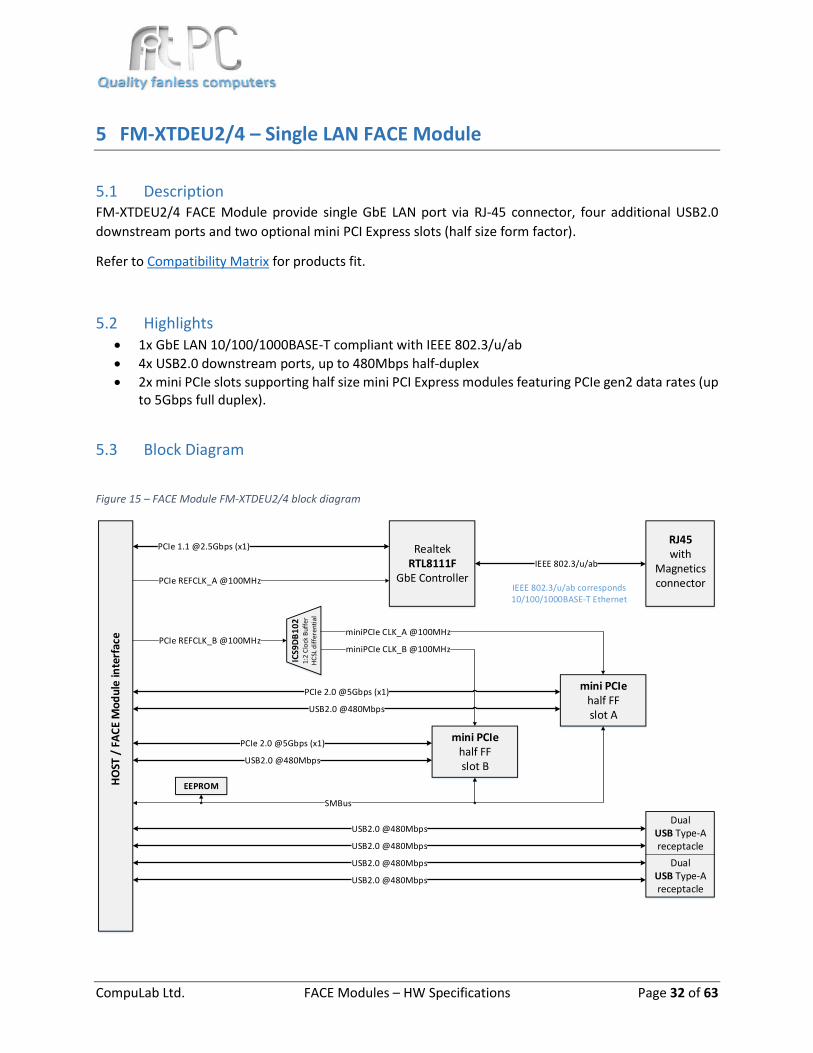
5.1 Description FM-XTDEU2/4 FACE Module provide single GbE LAN port via RJ-45 connector, four additional USB2.0
downstream ports and two optional mini PCI Express slots (half size form factor).
Refer to Compatibility Matrix for products fit.
5.2 Highlights 1x GbE LAN 10/100/1000BASE-T compliant with IEEE 802.3/u/ab
4x USB2.0 downstream ports, up to 480Mbps half-duplex
2x mini PCIe slots supporting half size mini PCI Express modules featuring PCIe gen2 data rates (up to 5Gbps full duplex).
5.3 Block Diagram
Figure 15 – FACE Module FM-XTDEU2/4 block diagram
HO
ST /
FA
CE
Mo
du
le in
terf
ace
USB2.0 @480Mbps
RJ45 with
Magneticsconnector
USB2.0 @480Mbps
USB2.0 @480Mbps
USB2.0 @480Mbps
PCIe REFCLK_A @100MHz
miniPCIe CLK_B @100MHz
Realtek RTL8111F
GbE Controller
PCIe 1.1 @2.5Gbps (x1)
IEEE 802.3/u/ab
EEPROM
SMBus
PCIe REFCLK_B @100MHz
DualUSB Type-A receptacle
PCIe 2.0 @5Gbps (x1)
USB2.0 @480Mbps
PCIe 2.0 @5Gbps (x1)
ICS9
DB
10
21
:2 C
lock
Buf
fer
HC
SL d
iffer
enti
al
mini PCIe half FFslot B
mini PCIehalf FFslot A
USB2.0 @480Mbps
miniPCIe CLK_A @100MHz
IEEE 802.3/u/ab corresponds 10/100/1000BASE-T Ethernet
DualUSB Type-A receptacle
CompuLab Ltd. FACE Modules – HW Specifications Page 33 of 63
5.4 Hardware Specifications The following section provides information about FM-XTDEU2/4 main components and features.
5.4.1 Realtek RTL8111F GbE Controller The Realtek RTL8111F Gigabit Ethernet controller combines a triple-speed IEEE 802.3 compliant Media
Access Controller (MAC) with a triple-speed Ethernet transceiver, PCI Express bus controller, and
embedded memory. With state-of-the-art DSP technology and mixed-mode signal technology, the
RTL8111F offers high-speed transmission over CAT 5 UTP cable.
The RTL8111F supports PCI Express 1.1 bus interface for host communications with power management,
and is compliant with the IEEE 802.3u specification for 10/100Mbps Ethernet and the IEEE 802.3ab
specification for 1000Mbps Ethernet. It also supports an auxiliary power auto-detect function, and will
auto-configure related bits of the PCI power management registers in PCI configuration space. The
RTL8111F features embedded One-Time-Programmable (OTP) memory to replace the external EEPROM.
Advanced Configuration Power management Interface (ACPI) – power management for modern operating
systems that are capable of Operating System-directed Power Management (OSPM) – is supported to
achieve the most efficient power management possible. In addition to the ACPI feature, remote Wake on
LAN is supported in both ACPI and APM (Advanced Power Management) environments.
The RTL8111F is suitable for multiple market segments and emerging applications, such as desktop,
mobile, workstation, server, communications platforms and embedded applications.
Main Features
— Integrated 10/100/1000 transceiver
— Auto-Negotiation with Next Page capability
— Supports PCI Express 1.1
— Supports pair swap/polarity/skew correction
— Crossover Detection & Auto-Correction
— Wake-on-LAN and remote wake-up support
— Supports Full Duplex flow control (IEEE 802.3x)
— Supports jumbo frame to 9K bytes
— Fully compliant with IEEE 802.3, IEEE 802.3u, IEEE 802.3ab
— Supports IEEE 802.1P Layer 2 Priority Encoding
— Supports IEEE 802.1Q VLAN tagging
— Supports IEEE 802.3az-2010 (EEE)
— Embedded OTP memory can replace the external EEPROM
— Supports power down/link down power saving/PHY disable mode
— Built-in switching regulator
— Supports Customized LEDs
— Supports 1-Lane 2.5Gbps PCI Express Bus
— Supports hardware ECC (Error Correction Code) function
— Supports hardware CRC (Cyclic Redundancy Check) function
— 48-pin QFN ‘Green’ package
CompuLab Ltd. FACE Modules – HW Specifications Page 34 of 63
5.4.2 IDT ICS9DB102 1-to-2 Differential Clock Driver IDT ICS9DB102 is two output clock buffer for PCIe Gen1 & Gen2 with HCSL current mode differential
outputs.
Device zero-delay buffer supports PCI Express clocking requirements. The ICS9DB102 is driven by a
differential compliant input clock. It attenuates jitter on the input clock and has a selectable PLL Band
Width to maximize performance in systems with or without Spread-Spectrum clocking.
5.5 Mechanics
5.5.1 PCB Assembly Figure 16 – FM-XTDEU2/4 PCB Assembly Top
5.5.2 Front Panel
Figure 17 – FM-XTDEU2/4 front panel drawing
CompuLab Ltd. FACE Modules – HW Specifications Page 35 of 63
5.6 Software Drivers
Windows Drivers
http://www.fit-pc2.com/download/fit-PC3/Win7/drivers/fit-PC3_Win7_Ethernet_2012.12.04.zip
Linux Drivers
— Implemented in Linux Kernel

CompuLab Ltd. FACE Modules – HW Specifications Page 36 of 63
6 FM-XTDE4U2/4 – Quad LAN FACE Module
6.1 Description FM-XTDE4U2/4 FACE Module incorporates 4 ports of GbE LAN supporting 10/100/1000BASE-T Ethernet
connectivity and compliant with IEEE 802.3/u/ab standard through a market regular RJ-45 connectors. It
also features 4 additional USB2.0 downstream ports supporting data rates up to 480Mbps.
Refer to Compatibility Matrix for products fit.
6.2 Highlights 4x GbE LAN 10/100/1000BASE-T compliant with IEEE 802.3/u/ab
4x USB2.0 downstream ports, up to 480Mbps half-duplex
6.3 Block Diagram
Figure 18 – FACE Module FM-XTDE4U2/4 block diagram
HO
ST /
FA
CE
Mo
du
le in
terf
ace
USB2.0 @480Mbps
Quad RJ45 with
MagneticsConnector
USB2.0 @480Mbps
USB2.0 @480Mbps
USB2.0 @480Mbps
PI6
C2
040
01
:4 C
lock
Dri
ver
CM
L di
ffer
enti
al
PCIe REFCLK @100MHz
PCIe CLK_1 @ 100MHz
PCIe CLK_2 @ 100MHz
PCIe CLK_3 @ 100MHz
PCIe CLK_4 @ 100MHz
82574L Intel GbE Controller
82574L Intel GbE Controller
82574L Intel GbE Controller
82574L Intel GbE Controller
PCIe 1.1 @2.5Gbps (x1)
PCIe 1.1 @2.5Gbps (x1)
PCIe 1.1 @2.5Gbps (x1)
IEEE 802.3/u/ab
PCIe 1.1 @2.5Gbps (x1)
SPI Nor Flash
SPI Nor Flash
SPI Nor Flash
SPI Nor Flash
SPI
IEEE 802.3/u/ab
IEEE 802.3/u/ab
IEEE 802.3/u/ab
EEPROMIEEE 802.3/u/ab corresponds 10/100/1000BASE-T Ethernet
SMBus
SPI
SPI
SPI
DualUSB Type-A receptacle
DualUSB Type-A receptacle

CompuLab Ltd. FACE Modules – HW Specifications Page 37 of 63
6.4 Hardware Specifications The following section provides information about FM-XTDE4U2/4 main components and features.
6.4.1 Intel 82574L GbE Controller The 82574L is a single, compact, low power component that offer a fully-integrated Gigabit Ethernet
Media Access Control (MAC) and Physical Layer (PHY) port. The 82574L uses the PCI Express* (PCIe*)
architecture and provides a single-port implementation in a relatively small area so it can be used for
server and client configurations as a LAN on Motherboard (LOM) design. The 82574L can also be used in
embedded applications such as switch add-on cards and network appliances.
MAC
— Flow Control Support compliant with the 802.3x specification
— VLAN support compliant with the 802.1Q specification
— MAC Address filters: perfect match unicast filters; multicast hash filtering, broadcast filter and
promiscuous mode
— MAC loopback
PHY
— Compliant with the 1 Gbps IEEE 802.3 802.3u, 802.3ab specifications
— IEEE 802.3ab auto negotiation support
— Full duplex operation at 10/100/1000 Mbps
— Half duplex at 10/100 Mbps
— Auto MDI, MDI-X crossover at all speeds
High Performance
— TCP segmentation capability compatible with Large Send offloading features
— Support up to 256 KB TCP segmentation (TSO v2)
— Fragmented UDP checksum offload for packet reassemble
— IPv4 and IPv6 checksum offload support (receive, transmit, and large send)
— Split header support
— 40KB packet buffer size
Manageability
— NC-SI for remote management core
— SMBus advanced pass through interface
Low Power
— Magic Packet wake-up enable with unique MAC address
— ACPI register set and power down functionality supporting D0 andD3 states
— Full wake up support (APM and ACPI 2.0)
— Smart power down at S0 no link and Sx no link
— LAN disable function
Technology
— 9 mm x 9 mm 64-pin QFN package with Exposed Pad
— Configurable LED operation for customization of LED displays

CompuLab Ltd. FACE Modules – HW Specifications Page 38 of 63
6.4.2 Pericom PI6C20400 1-to-4 Differential Clock Driver Pericom Semiconductor's PI6C20400 is a high-speed, low-noise differential clock driver/buffer compatible
with CML and HCSL differential I/O technology.
The device distributes a differential input clock to four differential pairs of clock outputs either with or
without PLL. The clock outputs are controlled by input selection of several static control signals and Host
SMBus interface. The device oriented and designed for PCI Express applications.
6.4.3 SPI NOR Flash The 82574L requires non-volatile memory content for initialization and configuration. The NVM is
connected to a single Serial Peripheral Interface (SPI). The 82574L is compatible with many sizes of 4-wire
SPI NVM devices. The required NVM size is dependent upon system requirements. FM-XTDE4U2/4 NVM
is implemented with Winbond W25Q80BL 8Mbit Flash memory.
CompuLab Ltd. FACE Modules – HW Specifications Page 39 of 63
6.5 Mechanics
6.5.1 PCB Assembly Figure 19 – FM-XTDE4U2/4 PCB Assembly Top
6.5.2 Front Panel
Figure 20 – FM-XTDE4U2/4 front panel drawing

CompuLab Ltd. FACE Modules – HW Specifications Page 40 of 63
6.6 Software Drivers
Windows Drivers
http://www.fit-pc2.com/download/fit-PC3/Win7/drivers/fit-PC3%20Win7%20FM-
LAN%202013.07.30.zip
Linux Drivers
— Implemented in Linux Kernel
CompuLab Ltd. FACE Modules – HW Specifications Page 41 of 63
7 FM-XTDM2 – Dual Mini PCI Express FACE Module
7.1 Description FM-XTDM2 FACE Module provide two optional mini PCI Express slots supporting either full or half size
mechanical form factor. By default arrive with mechanical latches for full size modules, but can be
adjusted for half size as well.
Refer to Compatibility Matrix for products fit.
7.2 Highlights 2x mini PCIe slots supporting mini PCI Express modules, featuring PCIe gen2 data rates (up to
5Gbps full duplex). Full/half size modules mechanical form factor
7.3 Block Diagram Figure 21 – FACE Module FM-XTDM2 block diagram
HO
ST /
FA
CE
Mo
du
le in
terf
ace
miniPCIe CLK_B @100MHz
EEPROM
SMBus
PCIe REFCLK_B @100MHz
PCIe 2.0 @5Gbps (x1)
USB2.0 @480Mbps
PCIe 2.0 @5Gbps (x1)
ICS9
DB
10
21
:2 C
lock
Buf
fer
HC
SL d
iffer
enti
al
mini PCIehalf/full FF
slot B
mini PCIe half/full FF
slot AUSB2.0 @480Mbps
miniPCIe CLK_A @100MHz

CompuLab Ltd. FACE Modules – HW Specifications Page 42 of 63
7.4 Hardware Specifications
7.4.1 Mini PCI Express Slot
Table 9 – mini PCI Express edge connector pinout
mini PCI Express edge connector
Pin # Pin Name Signal Description Pin # Pin Name Signal Description
1 WAKE# Open drain, active low signal driven low by a mini PCIe card to reactivate the PCIe link 2 3.3Vaux 3.3V power rail
3 COEX1/Reserved Reserved for future wireless coexistence control interface between radios (if needed)
4 GND Ground connection
5 COEX2/Reserved 6 1.5V 1.5V power rail
7 CLKREQ#
Clock request - open drain, active low driven by mini PCIe card to request PCIe reference clock 8 UIM_PWR/Reserved
The UIM signals are defined on the system connector to provide the interface between the removable User Identity Module (UIM) Interface - an extension of SIM and WWAN.
9 GND Ground connection 10 UIM_DATA/Reserved
11 REFCLK- Reference clock used to assist the synchronization of PCI Express interface timing circuits
12 UIM_CLK/Reserved
13 REFCLK+ 14 UIM_RESET/Reserved
15 GND Ground connection 16 UIM_VPP/Reserved
Mechanical Notch Key
17 Reserved/UIM_C8 Reserved 18 GND Ground connection
19 Reserved/UIM_C4 Reserved 20 W_DISABLE#
Active low signal when asserted by the system disable radio operation. Reserved for future use.
21 GND Ground connection 22 PERST# Asserted when power is switched off and also can be used by the system to force HW reset
23 PERn0
PCI Express differential receive pair
24 3.3Vaux 3.3V power rail
25 PERp0 26 GND Ground connection
27 GND Ground connection 28 1.5V 1.5V power rail
29 GND Ground connection 30 SMB_CLK Optional SMBus two-wire interface for Host/mini PCIe module communication 31 PETn0
PCI Express differential transmit pair
32 SMB_DATA
33 PETp0 34 GND Ground connection
35 GND Ground connection 36 USB_D-
USB Host Interface 37 GND Ground connection 38 USB_D+
39 3.3Vaux 3.3V power rail 40 GND Ground connection
41 3.3Vaux 3.3V power rail 42 LED_WWAN#
Active low output signals are provided to allow status indications to users via system provided LEDs
43 GND Ground connection 44 LED_WLAN#
45 Reserved
Reserved for future second PCI Express Lane
46 LED_WPAN#
47 Reserved 48 1.5V 1.5V power rail
49 Reserved 50 GND Ground connection
51 Reserved 52 3.3Vaux 3.3V power rail

CompuLab Ltd. FACE Modules – HW Specifications Page 43 of 63
7.5 Mechanics
7.5.1 PCB Assembly Figure 22 – FM-XTDM2 PCB Assembly Top
7.5.2 Front Panel When FM-XTDM2 FACE module installed a blank front panel cover is used.

CompuLab Ltd. FACE Modules – HW Specifications Page 44 of 63
8 FM-VC – Video Capture FACE Module
8.1 Description FM-VC FACE Module provide the ability for Video and Audio real and non-real time capture from low cost
analog video sensors. Features A/V sampling, video, image processing and motion detection algorithms.
In addition to application specific capabilities FM-VC offers several general purpose connectivity options
as dual USB2.0 downstream ports and serial port supporting either single ended RS232 or differential
mode RS485/RS422 operation.
FM-VC FACE Module designed for surveillance, homeland security and any other video analytic system.
Refer to Compatibility Matrix for products fit.
8.2 Highlights 8x Real time capture Composite Analog Video NTSC/PAL/SECAM channels
16x Non-real time capture Composite Analog Video NTSC/PAL/SECAM channels
8x Real time capture Analog Audio channels
2x DB15 female connectors for AV capture
2x USB2.0 downstream ports, up to 480Mbps half-duplex
1x Serial port supporting RS232/RS422/RS488 communication via RJ11
CompuLab Ltd. FACE Modules – HW Specifications Page 45 of 63
8.3 Block Diagram
Figure 23 – FACE Module FM-VC block diagram
HO
ST /
FA
CE
Mo
du
le in
terf
ace
USB2.0 @480Mbps
USB2.0 @480Mbps
PCIe 2.0 @5Gbps (x1)
EEPROMSMBus
PCIe REFCLK
DualUSB Type-A receptacle
ICS9
DB
10
21
:2 C
lock
Buf
fer
HC
SL d
iffe
ren
tial
miniPCIe CLK_A @100MHz
SMSC SIO1007-JVSuper-IO Controller
RJ11 JackADM3491
RS485/RS422 transceiver
LPC BUS @132Mbps
MAX3221 RS232
transceiverUART Serial COM
Differential/Single ended Serial comm.
Multiplexed half-duplex Host IFLPC_ADD/DATA[3:0]LPC_CLK @33MHz, LPC_CTRLs
DB15 Female
connector
Composite Analog Video x8
Analog Audio x4
DB15 Female
connector
Composite Analog Video x8
Analog Audio x4
8-c
h V
ideo
Dec
oder
8-c
h A
udio
AD
C/
Cod
ec
Vid
eo
An
alog
MU
X
Au
dio
/Vid
eo
Pr
oces
sin
gD
MA
Con
trol
ler
Hos
t In
terf
ace
PC
Ie P
HY
Intersil TW6869 Video Decoder

CompuLab Ltd. FACE Modules – HW Specifications Page 46 of 63
8.4 Hardware Specifications The following section provides information about FM-VC main components and features.
8.4.1 Intersil TW6869 Video Decoder The TW6869 is a highly integrated solution that supports multi-channel video and audio capture
via PCI Express x1 interface for PC DVR system and video analytic application. It contains high
quality eight channel NTSC/PAL/SECAM video decoders that convert analog composite video signal
to digital component YCbCr data. Adaptive 4H comb filter for separating luminance and chrominance to
reduce cross noise artifacts.
TW6869 contains a high performance proprietary DMA controller that fully optimizes the utilization
of PCI Express x1 bandwidth and enables it to transfer video and audio data at a high throughput
rate that closely approaches the theoretical limit of PCI Express x1 interface. TW6869 is able to
simultaneously decode and transfer 8 real time video streams, or up to 16 channel non-real time video
streams in FM-VC application, plus 8 real time audio channel.
Video Decoder Features
— Accepts all NTSC(M/N/4.43) / PAL(B/D/G/H/I/K/L/M/N/60) standards with auto detection
— Integrated eight video analog anti-alias filters and 10-bit CMOS ADCs
— Color Transient Improvement, White peak AGC control
— Programmable hue, saturation, contrast, brightness and sharpness
— High quality proprietary fast video locking system for non-real-time application
— High performance adaptive 4H comb filters for all NTSC and PAL standards
Audio Codec Features
— Integrated eight audio ADCs
— 8/16 bit audio word length
— Sample audio with 8/16/32/44.1/48kHz
DMA Controller
— Highly-efficient DMA design can support up to 8 real time D1 video and 8 real time audio
Channels, or up to 32 non-real- time video with optimization of full PCIe x1 bandwidth
— Multiple digital video format outputs: UYVY/Y422, YUYV/YUY2, IYU1/Y411, Y41P, YUV420,
RGB555 and RGB565
— Integrated internal video and audio generator simplifies system test and development
— Built-in motion detection engine for each video channel
Host Interface
— PCI Express Base Specification 1.1 and 2.0 Compliant

CompuLab Ltd. FACE Modules – HW Specifications Page 47 of 63
Figure 24 – Intersil TW6869 functional block diagram

CompuLab Ltd. FACE Modules – HW Specifications Page 48 of 63
8.4.2 SMSC SIO1007 Super-IO Controller The SMSC SIO1007 is PC 99 and ACPI 1.0 compliant Super I/O Controller. The SIO1007 implements the LPC
interface with the LPC PortSwitch interface. The LPC PortSwitch interface is a hot switchable external
docking LPC interface. It also features a full 16bit internally decoded address bus, a Serial IRQ interface
with PCI clock support, relocatable configuration ports and three DMA channel options. The part also
includes 16 GPIO pins.
The SIO1007 incorporates one complete 8-pin UART. In addition SIO1007 provides a second UART to
support a serial Infrared interface that complies with IrDA v1.2 (Fast IR) and several other popular IR
formats.
Main Features
— One full function Serial port
— High Speed UART with Send/Receive 16-Byte FIFOs
— Support 230k and 460k Baud rates
— Programmable baud rate generator
— Modem control circuit
— IR communication controller
— LPC bus Host interface
— LPC PortSwitch interface
— Two IRQ input pins
— PC99a and ACPI 1.0 Compliant
— Intelligent Auto Power Management
— 16x GPIOs
Figure 25 – SMSC SIO1007 functional block diagram

CompuLab Ltd. FACE Modules – HW Specifications Page 49 of 63
8.4.3 IDT ICS9DB102 1-to-2 Differential Clock Driver IDT ICS9DB102 is two output clock buffer for PCIe Gen1 & Gen2 with HCSL current mode differential
outputs.
Device zero-delay buffer supports PCI Express clocking requirements. The ICS9DB102 is driven by a
differential compliant input clock. It attenuates jitter on the input clock and has a selectable PLL Band
Width to maximize performance in systems with or without Spread-Spectrum clocking.
8.4.4 MAX3221 RS232 Transceiver Single-channel RS232 serial protocol transceiver
Implementation RS232 PHY serial protocol port
Data rate of 250kbps or more
Low power operation and auto-shutdown
8.4.5 ADM3491 RS422/RS485 Transceiver Single-channel RS422/RS485 serial protocol transceiver
Implements RS422/RS485 PHY serial protocol
Supports full-duplex RS485 protocol with data rate of up to 10Mbps
Low power operation and auto-shutdown
8.4.6 DB15 Connectors Pinout Table 10 – DB15 Connector Pinout
Pin # Type Functionality Cable Connector*
P1
P1 - 1 Analog Input Audio 1 AI01
P1 - 2 Analog Input Audio 2 AI02
P1 - 3 - GND
P1 - 4 Analog Input Audio 3 AI03
P1 - 5 Analog Input Audio 4 AI04
P1 - 6 Analog Input Video 1A VI11
P1 - 7 Analog Input Video 2D VI12
P1 - 8 - GND
P1 - 9 Analog Input Video 3A VI13
P1 - 10 Analog Input Video 4D VI14
P1 - 11 Analog Input Video 1B VI21
P1 - 12 Analog Input Video 2C VI22
P1 - 13 - GND
P1 - 14 Analog Input Video 3B VI23
P1 - 15 Analog Input Video 4C VI24

CompuLab Ltd. FACE Modules – HW Specifications Page 50 of 63
P2
P2 - 1 Analog Input Audio 5 AI01
P2 - 2 Analog Input Audio 6 AI02
P2 - 3 - GND
P2 - 4 Analog Input Audio 7 AI03
P2 - 5 Analog Input Audio 8 AI04
P2 - 6 Analog Input Video 5D VI11
P2 - 7 Analog Input Video 6A VI12
P2 - 8 - GND
P2 - 9 Analog Input Video 7D VI13
P2 - 10 Analog Input Video 8A VI14
P2 - 11 Analog Input Video 5C VI21
P2 - 12 Analog Input Video 6B VI22
P2 - 13 - GND
P2 - 14 Analog Input Video 7C VI23
P2 - 15 Analog Input Video 8B VI24
8.4.7 RJ11 Connector Pinout RJ11 connector serial port pinout shown below. It can function as RS232 or as RS422/RS485. The FM-VC
is supplied with a cable for serial RJ11 port.
Table 11 – RJ11 connector pinout
RS232 RS485
Pin # Type Functionality Type Functionality
1 NC HIGH Z O TX-
2 - GND - GND
3 O TX O TX+
4 I RX I RX+
5 - GND - GND
6 NC HIGH Z I RX-

CompuLab Ltd. FACE Modules – HW Specifications Page 51 of 63
8.5 Cables The FM-VC is supplied with two DB15 to RCA and BNC cables, along with one RJ11 serial communication
cable.
8.5.1 DB15 to RCA and BNC Cables In order to connect the FM-VC to video/audio source, it is provided with two identical cables of DB15-
male to 8 BNC and 4 RCA connectors:
4 blue female BNC connectors for analog video input 4 green female BNC connectors for analog video input 4 red female RCA connectors for analog audio input
The signals and the matching connectors of the DB15 to RCA and BNC Cables are detailed in the table
below. Signal names are labeled on the cables.
Table 12 – DB15 to RCA and BNC Cable
Signal Name DB15 Pin # Functionality Type Connector Color
VI11 6 Video input BNC Blue
VI12 7 Video input BNC Blue
VI13 9 Video input BNC Blue
VI14 10 Video input BNC Blue
VI21 11 Video input BNC Green
VI22 12 Video input BNC Green
VI23 14 Video input BNC Green
VI24 15 Video input BNC Green
AI01 1 Audio input RCA Red
AI02 2 Audio input RCA Red
AI03 4 Audio input RCA Red
AI04 5 Audio input RCA Red
CompuLab Ltd. FACE Modules – HW Specifications Page 52 of 63
8.5.2 RJ11 to DB9 Cable The FM-VC is supplied with a RJ11 6P6C-male to DB9-female cable. This cable is compatible with RS232
standard rather with RS485/RS422 DB9 connector standard.
DB9 RS232 pinout shown below.
Figure 26 – RS232 DB9 Connector View
RX
TX
GND
CompuLab Ltd. FACE Modules – HW Specifications Page 53 of 63
8.6 Mechanics
8.6.1 PCB Assembly Figure 27 – FM-VC PCB Assembly Top
Figure 28 – FM-VC PCB Assembly Bottom
CompuLab Ltd. FACE Modules – HW Specifications Page 54 of 63
8.6.2 Front Panel Figure 29 – FM-VC front panel drawing

CompuLab Ltd. FACE Modules – HW Specifications Page 55 of 63
8.7 Software Drivers Windows Drivers
— TBD
Linux Drivers
— http://fit-pc.com/download/face-modules/fm-vc/sw/linux-drivers/tw68v-dkms_1.0_all.zip

CompuLab Ltd. FACE Modules – HW Specifications Page 56 of 63
9 FM-POE – Quad LAN with Power over Ethernet PSE ports
9.1 Description FM-POE FACE Module incorporates 4 ports of GbE LAN supporting 10/100/1000BASE-T Ethernet
connectivity, compliant with IEEE 802.3/u/ab standard. All four ports compliant with IEEE 802.3af*
support PoE and PoE + PSE applications. Two additional USB2.0 downstream ports supporting data rates
up to 480Mbps for general purpose connectivity.
Note that HW Rev1.0 supports PSE Class 0 (15.4W max) per port when 2 ports populated with PD Class 0
devices (12.95W max).
Refer to Compatibility Matrix for products fit.
9.2 Highlights 4x GbE LAN 10/100/1000BASE-T compliant with IEEE 802.3/u/ab
4x PSE ports compliant with IEEE 802.3af* PoE standard (see note above)
2x USB2.0 downstream ports, up to 480Mbps half-duplex
9.3 Block Diagram Figure 30 – FACE Module FM-POE block diagram
HO
ST /
FA
CE
Mo
du
le in
terf
ace
Quad RJ45PoE+PSE
with MagneticsConnector
USB2.0 @480Mbps
USB2.0 @480Mbps
PI6
C2
040
01
:4 C
lock
Dri
ver
CM
L di
ffer
enti
al
PCIe REFCLK @100MHz
PCIe CLK_1 @ 100MHz
PCIe CLK_2 @ 100MHz
PCIe CLK_3 @ 100MHz
PCIe CLK_4 @ 100MHz
I211AT/82574L
Intel GbE Controller
I211AT/82574L
Intel GbE Controller
I211AT/82574L
Intel GbE Controller
I211AT/82574L
Intel GbE Controller
PCIe 2.1 @5Gbps (x1)
PCIe 2.1 @5Gbps (x1)
PCIe 2.1 @5Gbps (x1)
IEEE 802.3/u/ab; IEEE 802.3af*
PCIe 2.1 @5Gbps (x1)
SPI Nor Flash
SPI Nor Flash
SPI Nor Flash
SPI Nor Flash
SPI
IEEE 802.3/u/ab; IEEE 802.3af*
IEEE 802.3/u/ab; IEEE 802.3af*
IEEE 802.3/u/ab; IEEE 802.3af*
EEPROM
SPI
SPI
SPI
DualUSB Type-A receptacle
Power InDC Jack
LT3757AInverting Boost
12VDC
12VDC
Si3452Quad HV PoE Controller for
PSE ports
-48VDC
-48VDC
-48VDC
-48VDC
I2C/SMBus
-48VDC
Port A_HV
POE_RSTnPOE_INTn
Port B_HV
Port C_HV
Port D_HV
PSE
Hig
h V
olt
age
SPI Flash compatible with 82574L GbE only

CompuLab Ltd. FACE Modules – HW Specifications Page 57 of 63
9.4 Hardware Specifications The following section provides information about FM-POE main components and features.
9.4.1 Intel I211AT GbE Controller Intel Ethernet I211 controller is a single port, compact, low power component that supports GbE designs.
The I211 offers a fully-integrated GbE Media Access Control (MAC), Physical Layer (PHY) port and supports
PCI Express 2.1 (5GT/s). The I211 enables 1000BASE-T implementations using an integrated PHY. It can be
used for server system configurations such as rack mounted or pedestal servers, in an add-on NIC or LAN
on Motherboard (LOM) design. Another possible system configuration is for blade servers as a LOM or
mezzanine card. It can also be used in embedded applications such as switch add-on cards and network
appliances.
One independent interface is used to connect the I211 port to external devices. The following protocol is
supported: MDI (copper) support for standard IEEE 802.3 Ethernet interface for 1000BASE-T, 100BASE-TX,
and 10BASE-T applications (802.3, 802.3u, and 802.3ab).
Main Features
— PCIe v2.1 (5 GT/s) x1, with Switching Voltage Regulator (iSVR)
— Integrated Non-Volatile Memory (iNVM)
— Platform Power Efficiency
— IEEE 802.3az Energy Efficient Ethernet (EEE)
— Proxy: ECMA-393 and Windows logo for proxy offload
— Jumbo frames
— Interrupt moderation, VLAN support, IP checksum offload
— RSS and MSI-X to lower CPU utilization in multi-core systems
— Advanced cable diagnostics, auto MDI-X
— ECC – error correcting memory in packet buffers
— Four Software Definable Pins (SDPs)
For Intel 82574L GbE controller please refer to 6.4.1 section.
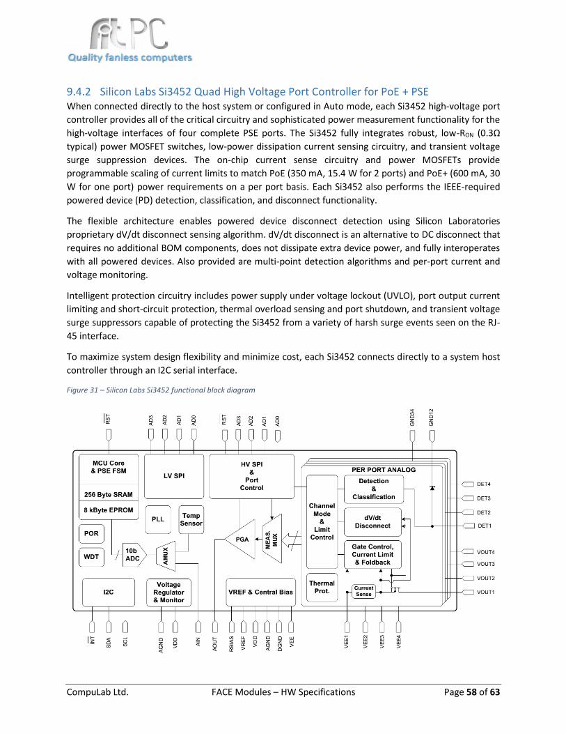
CompuLab Ltd. FACE Modules – HW Specifications Page 58 of 63
9.4.2 Silicon Labs Si3452 Quad High Voltage Port Controller for PoE + PSE When connected directly to the host system or configured in Auto mode, each Si3452 high-voltage port
controller provides all of the critical circuitry and sophisticated power measurement functionality for the
high-voltage interfaces of four complete PSE ports. The Si3452 fully integrates robust, low-RON (0.3Ω
typical) power MOSFET switches, low-power dissipation current sensing circuitry, and transient voltage
surge suppression devices. The on-chip current sense circuitry and power MOSFETs provide
programmable scaling of current limits to match PoE (350 mA, 15.4 W for 2 ports) and PoE+ (600 mA, 30
W for one port) power requirements on a per port basis. Each Si3452 also performs the IEEE-required
powered device (PD) detection, classification, and disconnect functionality.
The flexible architecture enables powered device disconnect detection using Silicon Laboratories
proprietary dV/dt disconnect sensing algorithm. dV/dt disconnect is an alternative to DC disconnect that
requires no additional BOM components, does not dissipate extra device power, and fully interoperates
with all powered devices. Also provided are multi-point detection algorithms and per-port current and
voltage monitoring.
Intelligent protection circuitry includes power supply under voltage lockout (UVLO), port output current
limiting and short-circuit protection, thermal overload sensing and port shutdown, and transient voltage
surge suppressors capable of protecting the Si3452 from a variety of harsh surge events seen on the RJ-
45 interface.
To maximize system design flexibility and minimize cost, each Si3452 connects directly to a system host
controller through an I2C serial interface.
Figure 31 – Silicon Labs Si3452 functional block diagram

CompuLab Ltd. FACE Modules – HW Specifications Page 59 of 63
9.4.3 Pericom PI6C20400 1-to-4 Differential Clock Driver Pericom Semiconductor's PI6C20400 is a high-speed, low-noise differential clock driver/buffer compatible
with CML and HCSL differential I/O technology.
The device distributes a differential input clock to four differential pairs of clock outputs either with or
without PLL. The clock outputs are controlled by input selection of several static control signals and Host
SMBus interface. The device oriented and designed for PCI Express applications.
9.4.4 SPI NOR Flash SPI Flash Reserved for pin compatible 82574L GbE device.
The 82574L requires non-volatile memory content for initialization and configuration. The NVM is
connected to a single Serial Peripheral Interface (SPI). The 82574L is compatible with many sizes of 4-wire
SPI NVM devices. The required NVM size is dependent upon system requirements. FM-XTDE4U2/4 NVM
is implemented with Winbond W25Q80BL 8Mbit Flash memory.
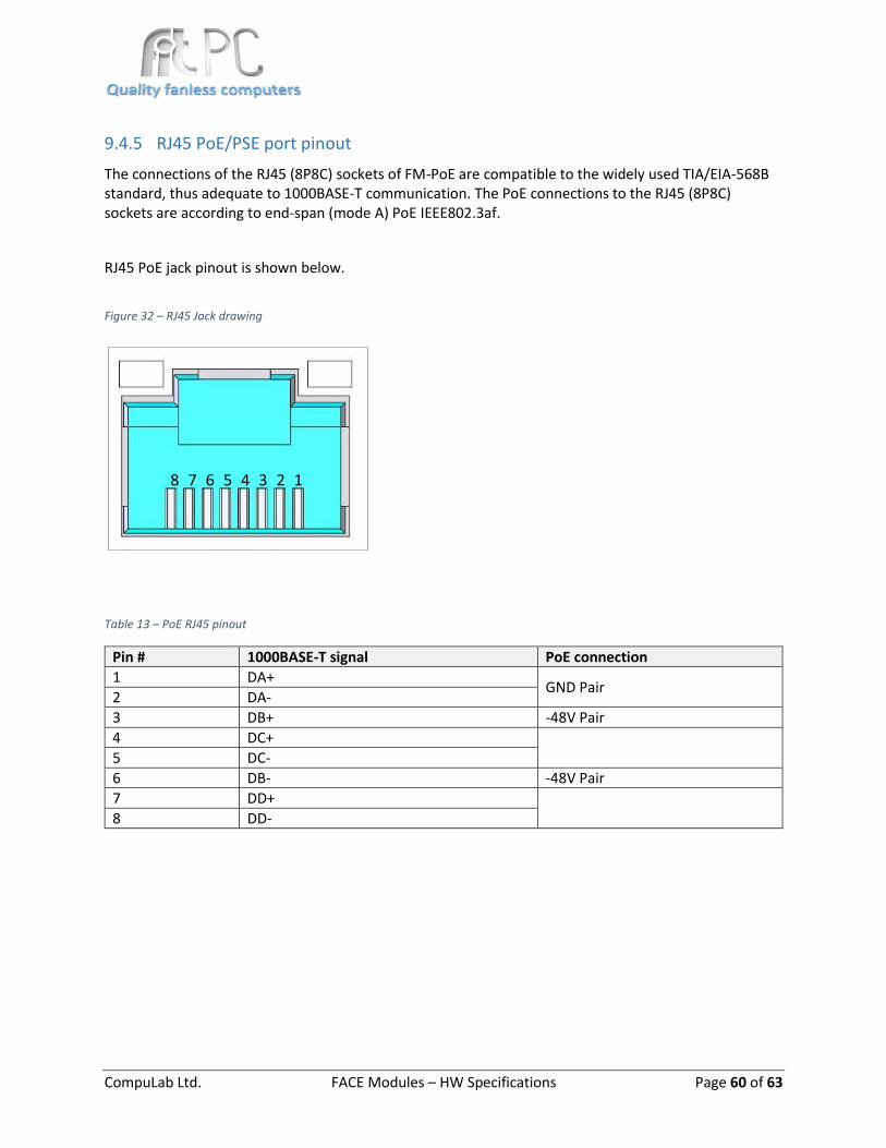
CompuLab Ltd. FACE Modules – HW Specifications Page 60 of 63
9.4.5 RJ45 PoE/PSE port pinout
The connections of the RJ45 (8P8C) sockets of FM-PoE are compatible to the widely used TIA/EIA-568B standard, thus adequate to 1000BASE-T communication. The PoE connections to the RJ45 (8P8C) sockets are according to end-span (mode A) PoE IEEE802.3af.
RJ45 PoE jack pinout is shown below.
Figure 32 – RJ45 Jack drawing
Table 13 – PoE RJ45 pinout
Pin # 1000BASE-T signal PoE connection
1 DA+ GND Pair
2 DA-
3 DB+ -48V Pair
4 DC+
5 DC-
6 DB- -48V Pair
7 DD+
8 DD-
8 7 6 5 4 3 2 1

CompuLab Ltd. FACE Modules – HW Specifications Page 61 of 63
9.5 Mechanics
9.5.1 PCB Assembly Figure 33 – FM-POE PCB Assembly Top
9.5.2 Front Panel Figure 34 – FM-POE front panel drawing
PoE 2 LED PoE 1 LED
PoE 3 LED
Power Jack
PoE 0 LED
USB 2.0
USB 2.0
Power LED
LAN 0 LAN 1 LAN 2 LAN 3
CompuLab Ltd. FACE Modules – HW Specifications Page 62 of 63
9.6 Software Drivers
Windows Drivers
TBD
Linux Drivers
— Implemented in Linux Kernel
9.7 Safety Information On every use of FM-POE to deliver Power over Ethernet, 12V power supply must be applied to the power
jack on the front panel of FM-POE. The use of PoE with the power supplied via the system board back
panel may result in permanent damage to the system.

CompuLab Ltd. FACE Modules – HW Specifications Page 63 of 63
10 Reference
Schematics files can be downloaded and serve as reference design documents.
Table 14 – Reference design schematics
Schematics Board Revision
Reference location
FM-4USB 1.1 http://fit-pc.com/download/face-modules/fm-4usb/hw/rev1.1/Schematics/fm4u_1v1.pdf
FM-USB3 2.1 http://fit-pc.com/download/face-modules/fm-usb3/hw/rev2.1/fm-usb3_2_1.pdf
FM-SER 1.1 http://fit-pc.com/download/face-modules/fm-ser/hw/rev1.1/Schematics/fm-ser_1v1.pdf
FM-XTDEU2/4
1.1 http://fit-pc.com/download/face-modules/fm-1lan/hw/rev1.1/Schematics/FM-XTD_1V1.pdf
FM-XTDE4U2/4
1.1 http://fit-pc.com/download/face-modules/fm-4lan/hw/rev1.1/Schematics/FM-4LAN_1V1.pdf
FM-XTDM2 1.1 http://fit-pc.com/download/face-modules/fm-2pcie/hw/rev1.1/Schematics/FM-XTD_1V1.pdf
FM-VC 1.0 http://fit-pc.com/download/face-modules/fm-vc/hw/rev1.0/Schematics/fm_vc.pdf
FM-POE
1.0 TBD
Other Resources
FACE Modules compatibility matrix:
http://fit-pc.com/download/app-notes/app-note-products-fm-compatibility-matrix.pdf
For the latest revision of this document follow the link:
http://fit-pc.com/download/face-modules/documents/face-modules-hw-specifications.pdf
FACE Modules portfolio overview presentation:
http://fit-pc.com/download/face-modules/documents/face-modules-portfolio-overview.pdf