fabrication of large area nano-rings for mram application
TRANSCRIPT
Microelectronic Engineering 85 (2008) 1555–1560
Contents lists available at ScienceDirect
Microelectronic Engineering
journal homepage: www.elsevier .com/locate /mee
Fabrication of large area nano-rings for MRAM application
Yong Luo, Veena Misra *
Department of Electrical and Computer Engineering, North Carolina State University, Raleigh, NC 27695, USA
a r t i c l e i n f o
Article history:Received 24 June 2007Received in revised form 5 February 2008Accepted 1 March 2008Available online 19 March 2008
Keywords:Magnetic ringLateral etchDe-centered ring
0167-9317/$ - see front matter � 2008 Published bydoi:10.1016/j.mee.2008.03.004
* Corresponding author. Tel.: +1 919 515 5347.E-mail address: [email protected] (V. Misra).
a b s t r a c t
We have developed lateral etch techniques to fabricate large area high density nano-scale magnetic ringarrays by deep ultraviolet lithography. Both centered and de-centered rings have been obtained. Thewidth of the rings are controlled by the lateral etch time, and the inner ring diameter was scaled downbelow the lithography resolution limit. For de-centered rings, the shift between the center of inner andouter circles was easily adjustable. The characteristics of the ring arrays were characterized by SEM, AFMand SQUID.
� 2008 Published by Elsevier B.V.
Magnetic rings are of rapidly rising interest in recent years, dueto their promising applications in data storage, logic and sensingdevices. Two stable magnetic states in the rings are observed bysimulations and measurements: the flux-closure vortex state(clockwise and anti-clockwise configuration), and the onion state(two opposite head-on domain walls). The switching betweenthese states has been found to be reproducible, simple, and fast[1]. This property has been proposed for magnetic random accessmemory (MRAM) utilization [2]. The two stable vortex stateswhere the field lines encircle the center to form either clockwiseor counter-clockwise formations were proposed as data storage,i.e., 1 s and 0 s. Research activities on magnetic rings have shownthat the switching field is dependent on the diameter, width andthickness of the rings [3–8]. Magnetic rings with outer diametersof 90 nm and width of 30 nm have been reported to have stablevortex states [9]. Thus for device applications such as data storage,the size of the magnetic rings can be minimized to achieve the highdensities required. Furthermore, it is important to prepare the vor-tex state with a desired direction of circulation, and several config-urations have been proposed for this vortex chirality control bymaking notches in the rings [10], introducing partially planed out-er sides [11,12], asymmetric square rings [13], and de-centeredrings [14,15]. Comparing these configurations, the de-centeredrings, whose inner hole is shifted from the center of the ring, arevery reliable in vortex chirality control.
Normally e-beam lithography is employed to fabricate nano-rings [6,9,16]. Other possible techniques include phase shift mask[17], multiple-beam achromatic interference lithography [18],nanospheres template [19] and porous alumina template [20].
Elsevier B.V.
For conventional photolithography technique, it becomes a chal-lenge to fabricate nano-rings with the scale near to the resolutionof the tool. For a dark mask with transparent ring regions, the innercircle (dark region) of the ring will be exposed totally due to theFraunhofer diffraction, while for a light mask which has ring regionas dark, the light intensity high enough to be able to expose theinner circle (transparent region) will damage all the dark ringregion. Therefore comparing to the resolution of the photolithogra-phy tool, the ring dimensions on the mask must be designed muchlarger to overcome these issues, leading to large scale and low den-sity. In this work, we reported a novel and simple technique tofabricate nano-rings using conventional mask photolithography.Using this, the problems mentioned above can be avoided andlarge area, high density of ordered nano-rings were obtained.De-centered rings were also fabricated by this method.
Our new technique is illustrated in Fig. 1. The substrate was firstcoated with a bottom antireflective coating layer (BARC) followedby photoresist. After exposure and develop, holes were patternedonto the photoresist layer, while the BARC layer was unattacked(Fig. 1a). Then a thin metal film (<10 nm) was deposited on thesamples by sputtering, which covered the top surface of both thephotoresist and the BARC layer, while keeping the sidewalls ofthe photoresist exposed (Fig. 1b). After that, the samples wereetched by oxygen plasma RIE. During the RIE etch, the sidewall ofthe photoresist was etched laterally, leading to the exposure ofthe BARC layer underneath the photoresist. The revealed BARC layerwas etched vertically in the oxygen plasma, resulting in anti-ringsin the BARC layer (Fig. 1c). After removing the photoresist layerby soaking into acetone with ultrasonic, which does not attackthe BARC, magnetic metal film can be deposited into the anti-ringson the BARC layer, and another lift-off process of BARC layer byultrasonic 5% NH4OH left the metal rings on the substrate (Fig. 1f).

BARCSi
(a’)
(b’)
(c’)
(d’)
(e’)
(f’)
PR PR PR
BARCSi
PR PR PRBARC
Si
PR PR PR
Si
Si
Si
Si
BARCSi
(a)
(b)
(c)
(d)
(e)
(f)
PR PR PR
BARCSi
PR PR PR
Si
Si
Si
Si
Centered Ring De-centered Ring
Fig. 1. Ring fabrication process. The de-centered ring process is similar as the centered ring process, except that the sample is titled a small angle h during RIE (step b). (a)After photolithography, deposit a thin layer of metal A on the sample; (b) RIE oxygen plasma dry etch; (c) Cross-section view after RIE etch; (d) Remove photoresist by soakinginto acetone with ultrasonic, and deposit magnetic metal film B on the BARC with anti-ring pattern; (e) Cross-section view after magnetic metal film B deposition; (f)Magnetic rings after lift-off.
Fig. 2. Top view of hole array patterned on the photoresist. (a) square lattice with 300 nm pitch; (b) triangular lattice with 375 nm pitch.
Fig. 3. After RIE oxygen plasma etch (a) cross-section view, which shows the lateral etch of photoresist and the anti-ring in the BARC layer; (b) top view, some photoresist waspeeled off to reveal the anti-ring in the BARC underneath. The hole size at the top surface of the photoresist does not change after etch.
1556 Y. Luo, V. Misra / Microelectronic Engineering 85 (2008) 1555–1560
In our experiment, the lithography was performed using ASML5500/950B scanner at 193 nm wavelength with 130 nm resolution.Samples were coated with 82 nm thick BARC (Brewer ScienceAR29A-8) followed by 400 nm thick photoresist (Rohm & HassV41). Two patterns, as shown in Fig. 2, the square lattice of hole ar-ray with pitch of 300 nm, and the triangular lattice of hole arraywith pitch of 375 nm, were used. The hole diameter is 130 nm.Both patterns areas were 1.1 mm � 1.3mm (on substrate). The
scanner allows for pattern transfer on to a whole 6 inch waferallowing for large area nanostructure formation. After sputtering5 nm nickel film as mask, the RIE etch is processed at 100 W,60 mtorr and 5 sccm oxygen. SEM images (Fig. 3) after etch clearlyshows the lateral etch of photoresist and anti-ring pattern in theBARC layer. The RIE etch time is controlled to tune the size of therings which allows for much smaller resolution compared tolithography. During the RIE lateral etch, the outer diameter of the

Y. Luo, V. Misra / Microelectronic Engineering 85 (2008) 1555–1560 1557
rings increased with etching time, while the inner diameter of therings decreased. Thus we could fabricate rings with dimensions ofinner circle and width below the resolution limit of the photoli-thography. Representative anti-rings in BARC with different sizesare shown in Fig. 4.
Fig. 4. Representative anti-rings in BARC obtained after different
Fig. 5. Representative magnetic rings after lift off with different inner diameter and widtwidth = 70 nm; (d) Din = 80 nm, width = 120 nm.
Finally magnetic metal cobalt films (9 nm and 20 nm thick)were sputtered onto the BARC layer and lifted off in ultrasonic5% NH4OH solution. Fig. 5 shows representative ring arrays afterlift off. Smaller width of rings are well isolated (for example,Fig. 5a and c), while larger width of rings would connect together
RIE etch time. (a) 2 min; (b) 2.3 min; (c) 2 min; (d) 2.8 min.
h; (a) Din = 90 nm, width = 80 nm; (b) Din = 50 nm, width = 125 nm; (c) Din = 90 nm,
-800 -600 -400 -200 0 200 400 600 800
-1.0
-0.5
0.0
0.5
1.0
Nor
mal
ized
Mag
netiz
atio
n
Field (mT)
Fig. 7. Representative measured hysteresis loop of ring array by SQUID.
1558 Y. Luo, V. Misra / Microelectronic Engineering 85 (2008) 1555–1560
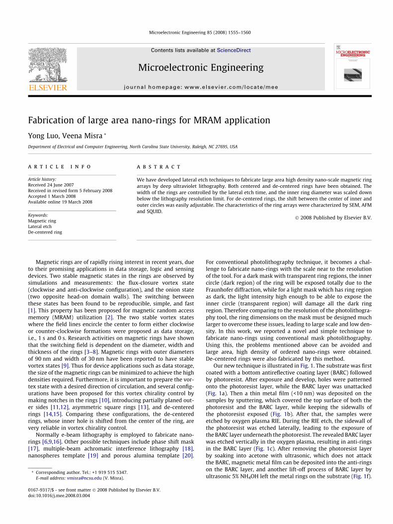
when the lateral etch time is long enough that the outer diameterreaches to the pitch of the hole pattern, as shown in Fig. 5b. Thethicknesses of the cobalt rings were examined by AFM (Fig. 6), alsoindicating the isolation of rings at 1 G/cm2.
The switching property of the fabricated ring arrays were char-acterized by SQUID (superconducting quantum interference de-vice). Representative hysteresis loop measured from thetriangular lattice ring array with outer diameter of 320 nm, innerdiameter of 80 nm and thickness of 20 nm (Fig. 5d) is shown inFig. 7. Here the curves in the field range of vortex state (between�100 and �500 mT) are distorted, which is believed due to theinteraction of adjacent rings because of small pitch/spacing [21].During the transition from stray-field-free vortex state to onionstate, some of the rings in the array will switch earlier due to theswitching distribution from dimension variation and defects. Theswitched rings (onion state) have stray field that adds to the exter-nal field and facilitate the switching of the adjacent ring. This re-sults in a chain reaction which switches the rings in a rowparallel to field direction from vortex state to onion state easierthan the single ring. To improve the hysteresis measurement, a lar-ger pitch (thus less interaction between rings) and thicker ring ar-rays would be helpful. However, the interaction in ring-shapedMRAM implementation will not be as bad since external magneticfield is only applied to selected cells, or spin torque transfer (STT)technology is utilized to switch between two vortex states directly.Therefore high density of rings is still desirable.
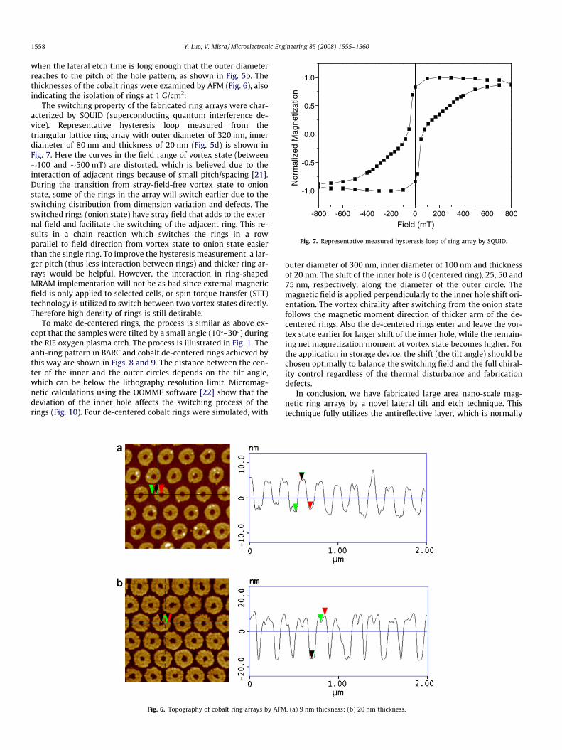
To make de-centered rings, the process is similar as above ex-cept that the samples were tilted by a small angle (10�–30�) duringthe RIE oxygen plasma etch. The process is illustrated in Fig. 1. Theanti-ring pattern in BARC and cobalt de-centered rings achieved bythis way are shown in Figs. 8 and 9. The distance between the cen-ter of the inner and the outer circles depends on the tilt angle,which can be below the lithography resolution limit. Micromag-netic calculations using the OOMMF software [22] show that thedeviation of the inner hole affects the switching process of therings (Fig. 10). Four de-centered cobalt rings were simulated, with
Fig. 6. Topography of cobalt ring arrays by AFM
outer diameter of 300 nm, inner diameter of 100 nm and thicknessof 20 nm. The shift of the inner hole is 0 (centered ring), 25, 50 and75 nm, respectively, along the diameter of the outer circle. Themagnetic field is applied perpendicularly to the inner hole shift ori-entation. The vortex chirality after switching from the onion statefollows the magnetic moment direction of thicker arm of the de-centered rings. Also the de-centered rings enter and leave the vor-tex state earlier for larger shift of the inner hole, while the remain-ing net magnetization moment at vortex state becomes higher. Forthe application in storage device, the shift (the tilt angle) should bechosen optimally to balance the switching field and the full chiral-ity control regardless of the thermal disturbance and fabricationdefects.
In conclusion, we have fabricated large area nano-scale mag-netic ring arrays by a novel lateral tilt and etch technique. Thistechnique fully utilizes the antireflective layer, which is normally
. (a) 9 nm thickness; (b) 20 nm thickness.

Fig. 8. Anti-ring pattern in the BARC layer with center shift as the tilt angle h changes during RIE etch, white arrows indicate the center shift direction. (a) h = 10�,shift = 15 nm; (b) h = 20�, shift = 35 nm; (c) h = 15�, shift = 25 nm; (d) h = 25�, shift = 75 nm.
Fig. 9. Cobalt de-centered rings. The white arrows indicate the center shift direction. (a) h = 10�, Dout = 240 nm, Din = 75 nm, shift = 10 nm; (b) h = 20�, Dout = 250 nm,Din = 55 nm, shift = 50 nm; (c) h = 10�, Dout = 340 nm, Din = 75 nm, shift = 12 nm; (d) h = 20�, Dout = 240 nm, Din = 85 nm, shift = 70 nm.
Y. Luo, V. Misra / Microelectronic Engineering 85 (2008) 1555–1560 1559
used in present photolithography process. The pitch (thus thedensity) of the rings could be determined by the resolution limitof photolithography, while the dimensions (the inner diameterand the width) of the rings can be scaled down by adjusting
the lateral etch time. This enables the possibility of fabricatinghigh density ordered ring-shaped magneto memories. Addition-ally, de-centered rings can also be made using similar technique,and the deviation between the center of the inner and outer cir-
(a)
(b)
(c)
(d)
M field
-200 -100 0 100 200
-1.0
-0.5
0.0
0.5
1.0
Nor
mal
ized
Mag
netiz
atio
n
Field (mT)
0 50nm 25nm 75nm
Fig. 10. Calculation of switching process for centered and de-centered cobalt rings with outer diameter of 300 nm, inner diameter of 100 nm and thickness of 20 nm.Magnetic field is in horizontal orientation. (a) concentric ring; (b) 25 nm shift; (c) 50 nm shift; (d) 75 nm shift.
1560 Y. Luo, V. Misra / Microelectronic Engineering 85 (2008) 1555–1560
cles can be controlled by the tilt angle during etch. This lateraletch technique utilizes the conventional masks, simplifying themask design and is compatible to the standard silicon process.This technique provides a new way to study magnetic nano-ringswith different parameters.
The authors thank David Vellenga for assistance with ASML5500/950B scanner lithography.
Acknowledgement
We would like to acknowledge the National Science Foundation(ECCS 0326221) for their support.
References
[1] M. Klaui, C.A.F. Vaz, L. Lopez-Diaz, J.A.C. Bland, Journal of Physics: CondensedMatter 15 (21) (2003) R985–R1023.
[2] J.G. Zhu, Y.F. Zheng, G.A. Prinz, Journal of Applied Physics 87 (9) (2000) 6668–6673.
[3] L. Lopez-Diaz, J. Rothman, M. Klaui, J.A.C. Bland, IEEE Transactions onMagnetics 36 (5) (2000) 3155–3157.
[4] S.P. Li, D. Peyrade, M. Natali, A. Lebib, Y. Chen, U. Ebels, L.D. Buda, K. Ounadjela,Physical Review Letters 86 (6) (2001) 1102–1105.
[5] M. Klaui, L. Lopez-Diaz, J. Rothman, C.A.F. Vaz, J.A.C. Bland, Z. Cui, Journal ofMagnetism and Magnetic Materials 240 (1-3) (2002) 7–10.
[6] Y.G. Yoo, M. Klaui, C.A.F. Vaz, L.J. Heyderman, J.A.C. Bland, Applied PhysicsLetters 82 (15) (2003) 2470–2472.
[7] H. Hu, H. Wang, M.R. McCartney, D.J. Smith, Journal of Applied Physics 97 (5)(2005).
[8] F.J. Castano, C.A. Ross, A. Eilez, Journal of Physics D: Applied Physics 36 (17)(2003) 2031–2035.
[9] L.J. Heyderman, M. Klaui, B. Nohammer, C.A.F. Vaz, J.A.C. Bland, C. David,Microelectronic Engineering 73–74 (2004) 780–784.
[10] M. Klaui, J. Rothman, L. Lopez-Diaz, C.A.F. Vaz, J.A.C. Bland, Z. Cui, AppliedPhysics Letters 78 (21) (2001) 3268–3270.
[11] R. Nakatani, T. Yoshida, Y. Endo, Y. Kawamura, M. Yamamoto, T. Takenaga, S.Aya, T. Kuroiwa, S. Beysen, H. Kobayashi, Journal of Applied Physics 95 (11)(2004) 6714–6716.
[12] R. Nakatani, T. Yoshida, Y. Endo, Y. Kawamura, M. Yamamoto, T. Takenaga, S.Aya, T. Kuroiwa, S. Beysen, H. Kobayashi, Journal of Magnetism and MagneticMaterials 286 (2005) 31–36.
[13] A.S. Mani, D. Geerpuram, A. Domanowski, V. Baskaran, V. Metlushko,Nanotechnology 15 (10) (2004) S645–S648.
[14] E. Saitoh, M. Kawabata, K. Harii, H. Miyajima, T. Yamaoka, Journal of AppliedPhysics 95 (4) (2004) 1986–1988.
[15] A. Subramani, D. Geerpuram, V. Baskaran, J. Friedlund, V. Metlushko, PhysicaC-Superconductivity and Its Applications 437–38 (2006) 293–298.
[16] C.A. Ross, F.J. Castano, D. Morecroft, W. Jung, H.I. Smith, T.A. Moore, T.J.Hayward, J.A.C. Bland, T.J. Bromwich, A.K. Petford-Long, Journal of AppliedPhysics 99 (8) (2006).
[17] A.O. Adeyeye, N. Singh, S. Goolaup, Journal of Applied Physics 98 (9) (2005) 6.[18] H.H. Solak, Microelectronic Engineering 78–79 (2005) 410–416.[19] F.Q. Zhu, D.L. Fan, X.C. Zhu, J.G. Zhu, R.C. Cammarata, C.L. Chien, Advanced
Materials 16 (23–24) (2004). 2155.[20] K.L. Hobbs, P.R. Larson, G.D. Lian, J.C. Keay, M.B. Johnson, Nano Letters 4 (1)
(2004) 167–171.[21] J. Wang, A.O. Adeyeye, N. Singh, Applied Physics Letters 87 (26) (2005).[22] Available from: <http://math.nist.gov/oommf/>.