exploring approaches for the synthesis of few‐layered
TRANSCRIPT
REVIEW
1803758 (1 of 16) © 2019 WILEY-VCH Verlag GmbH & Co. KGaA, Weinheim
www.advmat.de
Exploring Approaches for the Synthesis of Few-Layered Graphdiyne
Jingyuan Zhou, Jiaqiang Li, Zhongfan Liu,* and Jin Zhang*
Dr. J. Zhou, Dr. J. Li, Prof. Z. Liu, Prof. J. ZhangCenter for NanochemistryBeijing Science and Engineering Center for NanocarbonsBeijing National Laboratory for Molecular SciencesCollege of Chemistry and Molecular EngineeringPeking UniversityBeijing 100871, P. R. ChinaE-mail: [email protected]; [email protected]
The ORCID identification number(s) for the author(s) of this article can be found under https://doi.org/10.1002/adma.201803758.
DOI: 10.1002/adma.201803758
is predicted to be a semiconductor material with a band gap of ≈0.46 eV with unique anisotropic properties, while α and β-GDY are predicted to Dirac materials with metallic behavior like graphene.[3,4] Spe-cifically, GDY, which would be exclusively discussed in this review, is an important member in GY family containing diacety-lenic linkages (CCCC) connecting adjacent benzene rings extending in 2D plane, and this theoretical model was first proposed by Haley in 1997.[5] Considering the heat of formation and complexity for synthesis, GDY is the most synthetically approachable one in GY family. With a heat of formation of 919.2 kJ mol−1, GDY is the most stable carbon allotrope con-taining diacetylenic linkages. Meanwhile, GDY can be formed from polymerizing of single kind of precursor molecule.
Planar GDY belongs to p6mm space group with an optimized lattice constant of a = b = 9.48 Å.[6,7] The lower density
of carbon atoms and different types of hybridization of GDY lead to more structural flexibility and weaker mechanical stiff-ness than those of graphene and the computational model also shows a temperature-dependent “ripple” of this flat network, which is quite similar to graphene, contributing a lot to the stability of GDY sheet.[8] As we know, the electronic structure of layered materials is highly sensitive to the stacking manner. According to DFT-GGA method, Zhang et al. reported that the stacking arrangements with highest and second highest stability for bilayer GDY are AB (β1) and AB (β2), respectively. And the ABA (γ1) configuration is the most stable one as for trilayer construction. Three different configurations of trilayer GDY are also presented with approximate stability, all showing semicon-ducting characteristics.[9] Li et al. also investigated the crystal structure of GDY using low-voltage transmission electron microscope (TEM) with low current density demonstrating the ABC stacking mode of multilayer GDY,[10] which is also coinci-dent with the results reported by Hiroshi et al.[11]
Band structure and transport properties of GDY have also been investigated based on different calculation methods, showing the existence of a direct band gap at Γ point of the Brillouin zone. Besides, the effective masses are relatively small for both conduction and valence bands, resulting in high car-rier mobility. The calculated in-plane intrinsic electron mobility can reach as high as 105 cm2 V−1 s−1 at room temperature, while the hole mobility is about an order of magnitude lower.[3] GDY is predicated to simultaneously possess high carrier mobility
Graphdiyne (GDY) is an emerging carbon allotrope in the graphyne (GY) family, demonstrating extensive potential applications in the fields of electronic devices, catalysis, electrochemical energy storage, and nonlinear optics. Synthesis of few-layered GDY is especially important for both electronic applications and structural characterization. This work critically summarizes the state-of-art of GDY and focuses on exploring approaches for few-layered GDY synthesis. The obstacles and challenges of GDY synthesis are also analyzed in detail. Recently developed synthetic methods are discussed such as i) the copper substrate-based method, ii) the chemical vapor deposition (CVD) method, iii) the interfacial construction method, and iv) the graphene-templated method. Throughout the discus-sion, the superiorities and limitations of different methods are analyzed comprehensively. These synthetic methods have provided considerable inspiration approaching synthesis of few-layered or single-layered GDY film. The work concludes with a perspective on promising research directions and remaining barriers for layer-controlled and morphology-controlled synthesis of GDY with higher crystalline quality.
Graphdiyne
1. Introduction
Carbon is the most fascinating element in the periodic table. The past decades have witnessed the flourishing development of carbon nanomaterials, such as fullerene, carbon nanotubes, and graphene, and the diversity of carbon hybridization states (sp, sp2, and sp3) allows the artistic design of carbon allotropes.[1,2] As a consequence of abundant outstanding properties of these diverse carbon allotropes, it has always been appealing to explore more extensively about the family of carbon.
Graphyne (GY) is a rapidly rising star in carbon family refer-ring to a class of 2D carbon allotropes, which are merely consist of sp and sp2 hybrid carbon atoms and due to the multiple com-bining forms of sp and sp2 hybrid carbon atoms, GY family includes diversity structures. For example, γ-graphdiyne (GDY)
Adv. Mater. 2019, 31, 1803758
© 2019 WILEY-VCH Verlag GmbH & Co. KGaA, Weinheim1803758 (2 of 16)
www.advmat.dewww.advancedsciencenews.com
and natural moderate band gap of 0.46–1.10 eV (according to different simulated methods),[12–14] facilitating it as an ideal candidate for electronic devices. Besides, with highly conju-gated structure, uniformly distributed topological pores, and unique diyne structure, GDY is forecasted to show fascinating superiorities in the fields of energy storage and transformation, catalysis, nonlinear optical, gas separation, etc.[15–18] Therefore, developing synthetic methods for GDY preparation and inves-tigating its basic physicochemical properties are of significant importance for both basic scientific researches and practical applications.
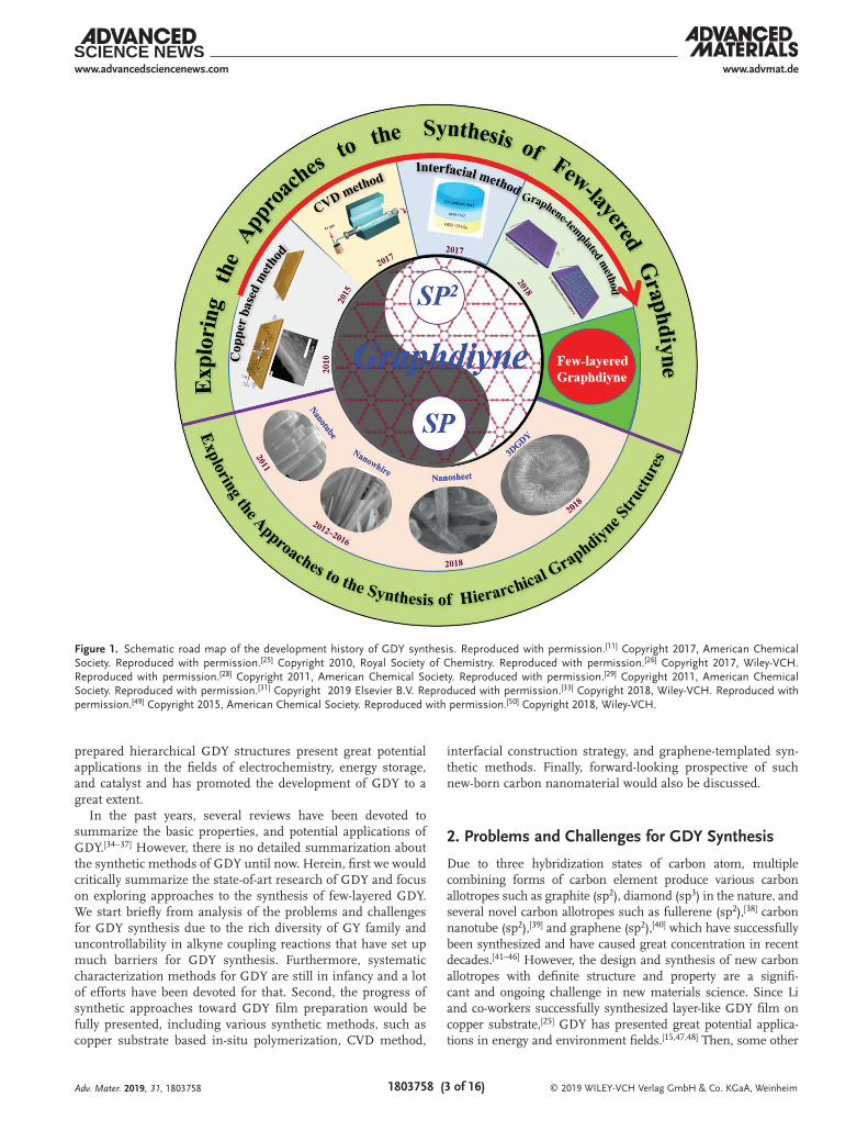
Reviewing the development of GDY synthesis, two main research routes can be easily distinguished (Figure 1). On the one hand, some scientists devoted much effort to developing methods for the synthesis of few-layered GDY film. One the other hand, some other scientists focus on the preparation of hierarchical GDY structures. The synthesis of few-layered, even single-layered, GDY is the ultimate goal because the ultrathin GDY plays a key role of study the intrinsic prop-erties of GDY. In this research timeline, we believe that the development of few-layered GDY synthesis could be conven-tionally divided into three periods. The first period began in 1997, when the GDY model was first proposed by Haley et al. After that, Haley and co-workers did a mountain of work about synthesis of annulenic subunits of GDY and investigated the optical properties and self-assembling behaviors of them.[19–23] However, with the limitation of tedious synthesis processes and decrease of solubility, only products with four carbon-rings could be obtained through these methods.[24] Much works about simulation of GDY also emerged during this period. While the synthesis of GDY encountered the bottleneck until year 2010 when Li et al. reported an in-situ polymerization method on Cu substrate, which could be denoted as the second period.[25] This ingenious method is viewed as a milestone in GDY history because it was not only the first time for synthesis of GDY as an applicable material, but also facilitated much progresses in applications of GDY. The beginning of the third period sprung up from 2017, when different strategies were proposed for GDY film preparation with high crystallinity. Inspired by CVD growth of graphene and on-surface covalent reaction in ultrahigh vacuum-scanning tunneling microscopy (UHV-STM) system, our group introduced a CVD synthetic method for growth of linked carbon monolayer with acetylenic scaffoldings by using hexaethynylbenzene (HEB) as precursor, which has provided a possible way for fabricating monolay-ered GDY.[26] By utilizing interfacial method (e.g., liquid/liquid and gas/liquid interface), GDY nanosheets were obtained with well-defined regular hexagonal domain shape and narrow domain size and thickness distribution, reflecting the good crystallinity and low oxygenic defect level.[11] Our group also developed a surface-templated method using graphene as an epitaxial template to induce coupling reaction in 2D extended plane.[27,28] By this mean, ultrathin GDY film was synthesized, which has brought light to the application of GDY film in electronic devices. Considering the extraordinary properties of GDY from theoretical prediction, the study of GDY appli-cations is another branch that would enhance the develop-ment of GDY and arouse more researchers’ interests. From the point of growth mechanism, scientists synthesized various
Jingyuan Zhou received her B.S. degree from the College of Chemistry, Nankai University in 2012 and Ph.D. degree from the Academy for Advanced Interdisciplinary Studies, Peking University in 2017. Her research during her Ph.D. was focused on the morphology and layer-controlled synthesis of high-quality graphdiyne.
Zhongfan Liu received his Ph.D. degree from the University of Tokyo in 1990. After a postdoctoral fellowship at the Institute for Molecular Science, Japan, he became an associate professor (1993), full professor (1993), and Cheung Kong Chair professor (1999) of Peking University. His research interests focus on
low-dimensional carbon materials and novel 2D atomic crystals, targeting nanoelectronic and energy conversion devices together with the exploration of fundamental phenomena in nanoscale systems.
Jin Zhang received his Ph.D. from Lanzhou University in 1997. After a two years postdoctoral fellowship at the University of Leeds, UK, he returned to Peking University where he was appointed Associate Professor (2000) and promoted to Full Professor in 2006. In 2013, he was appointed as Changjiang professor. He also is a Fellow
of the Royal Society of Chemistry. His research focuses on the controlled synthesis and spectroscopic characterization of carbon nanomaterials.
hierarchical GDY structures through controlling the catalyst diffusion and morphology of substrates. The pioneered hierar-chical GDY structure can date back to 2011, Li and co-workers first synthesized the GDY nanotubes using AAO template and controlling the diffusion direction of Cu based catalyst.[29] Afterward, 1D substrates were also employed for successfully synthesis of GDY nanowires.[30,31] In recent years, Li and Liu groups displayed the 3D GDY preparation using some 3D tem-plates, such as 3D Cu nanowires and diatomite.[32,33] These as
Adv. Mater. 2019, 31, 1803758
© 2019 WILEY-VCH Verlag GmbH & Co. KGaA, Weinheim1803758 (3 of 16)
www.advmat.dewww.advancedsciencenews.com
prepared hierarchical GDY structures present great potential applications in the fields of electrochemistry, energy storage, and catalyst and has promoted the development of GDY to a great extent.
In the past years, several reviews have been devoted to summarize the basic properties, and potential applications of GDY.[34–37] However, there is no detailed summarization about the synthetic methods of GDY until now. Herein, first we would critically summarize the state-of-art research of GDY and focus on exploring approaches to the synthesis of few-layered GDY. We start briefly from analysis of the problems and challenges for GDY synthesis due to the rich diversity of GY family and uncontrollability in alkyne coupling reactions that have set up much barriers for GDY synthesis. Furthermore, systematic characterization methods for GDY are still in infancy and a lot of efforts have been devoted for that. Second, the progress of synthetic approaches toward GDY film preparation would be fully presented, including various synthetic methods, such as copper substrate based in-situ polymerization, CVD method,
interfacial construction strategy, and graphene-templated syn-thetic methods. Finally, forward-looking prospective of such new-born carbon nanomaterial would also be discussed.
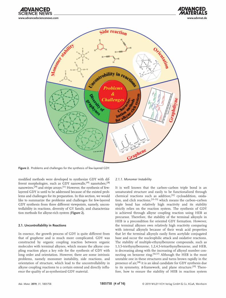
2. Problems and Challenges for GDY Synthesis
Due to three hybridization states of carbon atom, multiple combining forms of carbon element produce various carbon allotropes such as graphite (sp2), diamond (sp3) in the nature, and several novel carbon allotropes such as fullerene (sp2),[38] carbon nanotube (sp2),[39] and graphene (sp2),[40] which have successfully been synthesized and have caused great concentration in recent decades.[41–46] However, the design and synthesis of new carbon allotropes with definite structure and property are a signifi-cant and ongoing challenge in new materials science. Since Li and co-workers successfully synthesized layer-like GDY film on copper substrate,[25] GDY has presented great potential applica-tions in energy and environment fields.[15,47,48] Then, some other
Adv. Mater. 2019, 31, 1803758
Figure 1. Schematic road map of the development history of GDY synthesis. Reproduced with permission.[11] Copyright 2017, American Chemical Society. Reproduced with permission.[25] Copyright 2010, Royal Society of Chemistry. Reproduced with permission.[26] Copyright 2017, Wiley-VCH. Reproduced with permission.[28] Copyright 2011, American Chemical Society. Reproduced with permission.[29] Copyright 2011, American Chemical Society. Reproduced with permission.[31] Copyright 2019 Elsevier B.V. Reproduced with permission.[33] Copyright 2018, Wiley-VCH. Reproduced with permission.[49] Copyright 2015, American Chemical Society. Reproduced with permission.[50] Copyright 2018, Wiley-VCH.
© 2019 WILEY-VCH Verlag GmbH & Co. KGaA, Weinheim1803758 (4 of 16)
www.advmat.dewww.advancedsciencenews.com
modified methods were developed to synthesize GDY with dif-ferent morphologies, such as GDY nanowalls,[49] nanotubes,[28] nanowires,[29] and stripe arrays.[51] However, the synthesis of few-layered GDY is until to be addressed because of the existed prob-lems and challenges for its preparation. In this section, we would like to summarize the problems and challenges for few-layered GDY synthesis from three different viewpoints, namely, uncon-trollability in reactions, diversity of GY family, and characteriza-tion methods for alkyne-rich system (Figure 2).
2.1. Uncontrollability in Reactions
In essence, the growth process of GDY is quite different from that of graphene and is much more complicated. GDY was constructed by organic coupling reaction between organic molecules with terminal alkynes, which means the alkyne cou-pling reaction plays a key role for the synthesis of GDY with long order and orientation. However, there are some intrinsic problems, namely monomer instability, side reactions, and orientation of structure, which lead to the uncontrollability in alkyne coupling reactions to a certain extend and directly influ-ence the quality of as-synthesized GDY material.
2.1.1. Monomer Instability
It is well known that the carbon–carbon triple bond is an unsaturated structure and easily to be functionalized through chemical reactions such as addition,[52] cycloaddition, oxida-tion, and click reactions,[53–55] which means the carbon–carbon triple bond has relatively high reactivity and its stability strictly relies on the reaction system. The synthesis of GDY is achieved through alkyne coupling reaction using HEB as precursor. Therefore, the stability of the terminal alkynyls in HEB is a precondition for oriented GDY formation. However, the terminal alkynes own relatively high reactivity comparing with internal alkynyls because of their weak acid properties that let the terminal alkynyls easily form acetylide conjugated base and occur the nucleophilic attack and oxidative reactions. The stability of multiple-ethynylbenzene compounds, such as 1,3,5-triethynylbenzene, 1,2,4,5-tetraethynylbenzene, and HEB, is decreasing along with the increasing of alkynyl number con-necting on benzene ring.[56,57] Although the HEB is the most unstable one in these structures and turns brown rapidly in the presence of air,[58] it is an ideal candidate for GDY synthesis due to its symmetry, π-framework, and plane structure.[59] There-fore, how to ensure the stability of HEB in reaction system
Adv. Mater. 2019, 31, 1803758
Figure 2. Problems and challenges for the synthesis of few-layered GDY.
© 2019 WILEY-VCH Verlag GmbH & Co. KGaA, Weinheim1803758 (5 of 16)
www.advmat.dewww.advancedsciencenews.com
would be a very important issue for the synthesis of GDY with defined structure and is an ongoing challenge.
2.1.2. Side Reactions
As mentioned above, the terminal alkynyls are relatively reac-tive and sensitive compared with other carbon-carbon bonds due to it intrinsic characteristics. The high reactivity of mono mer would lead to some side reactions, which will intro-duce defects in the GDY structure resulting in poor crystallinity. Traditionally, the terminal alkynes are prone to occur oxidative addition, cyclotrimerization, and reductive elimination coupling reactions. Except reductive elimination coupling reaction, the others are two side reactions that will grievously impact the crys-tallinity of GDY structure if occurred. Palladium-catalyzed ter-minal alkyne coupling reactions turned to be an effective method for the synthesis of symmetrical 1,3-diynes.[60] However, side reac-tions (e.g., alkyne dimerization to diynes through head-to-head or head-to-tail coupling) are barely inhibited totally.[61] Except for solution process, side reactions are also observed in on-surface coupling reactions. Fuchs et al. synthesized linear oligomer/polymer chains through Glaser coupling on metal surface using the arylalkynes as starting materials.[62] Through STM characteri-zation, they identified several types of side products: hydroalky-nylation of the terminal alkyne at the α or β positions, dieneyne moieties, enediyne moieties, and trimerization products, which would lead to chain branching. Therefore, inhibiting these side reactions at the most extent when using HEB as precursor would be another key issue for high quality GDY preparation.
2.1.3. Orientation of Skeleton
Among various strategies of 2D materials, solution approaches have been proved to be a powerful one for GDY synthesis. How-ever, the synthesis process would go through a troublesome problem of free rotation of the alkyne-aryl single bonds, leading to the coexistence of coplanar and twisted frameworks. The orienta-tion of skeleton is a problem which should be addressed for the ultimate goal of a structurally perfect GDY. In solution approach, the HEB cannot rely on the ordering power of an interface and is not automatically arranged into the same plane if it is just placed at a flat liquid or solid surface.[63] When the coupling reac-tion occurred on terminal alkynyls, the central benzene rings of HEB would make the six coupling reactions occurred on the same plane. Therefore, there are some challenges that make it difficult to be a no perturbed 2D geometry of HEB. The first one is that it is comprehensible that all bond formations take place within this same plane for a small fragment. Whereas, when two such frag-ments meet and couple with each other, low rotation barrier exists at the connecting point, which means the fragments can freely rotate relative between them. This phenomenon will take place at their numerous lateral function groups along with growing fur-ther. Second, all critical bond-formation steps are difficult to occur just when the fragments happen to attain a coplanar conforma-tion, therefore unlikely lead to a structurally homogeneous new fragment. Third, the respective individual fragments and the rela-tive location of C are not easy or maybe impossible to covalently
capture the in-plane conformation during the actual growth situ-ation. These problems inevitably lead to formation of overlapping structures which eventually form 3D GDY networks. In order to solve these problems, the fragments to be connected must be forced automatically into one plane when coupling reactions occurred. However, above mentioned drawbacks are hard to be avoided in solution system. Considering the essences that GDY was constructed by organic coupling reaction between organic molecules, which means the orientation of organic molecules is a key role for long-range ordered GDY structure forming.[64] Using a template as grown substrate can control the orientation of organic molecules by taking advantage of template–molecule interaction that can effectively decrease the rotation barrier of the connecting bonds between fragments.[65,66] And the templated methods have been demonstrated as an effective method to syn-thesize oriented 2D materials.[64] Therefore, selecting an appro-priate template is very important considering the orientation of organic molecules at the interface and the interaction between monomers and template. In addition, the template method would be a promising methodology for few-layered GDY preparation.
2.2. Characterization Methods for Alkyne-Rich System
GDY, a new 2D carbon material, has aroused great concern since it was first synthesized in 2010. In order to obtain accu-rate and complete information of GDY, multiple characteriza-tion methods are required. In characterizing previous graphitic materials, Raman spectroscopy has exhibited remarkable advan-tages.[67,68] In the study of graphene, the Raman spectrum can be used to quickly and easily determine the layer number, quality of crystals, stacking pattern, and doping characteristics.[69] The typical Raman spectrum graphene contains two peaks at 1588 and 2693 cm−1 that are corresponding to G-band and 2D-band. Another peak would appear at 1350 cm−1 if the gra-phene has some defects. For single layer graphene, the 2D-band has higher intensity than G-band and is with perfectly sym-metrical single Lorentz peak. However, the full width at half maximum (FWHM) of 2D-band will increase along with the layer number increasing, which is resulted from the splitting of the electron energy band structure of multilayer graphene.[70] Additionally, the layer number of graphene could be identified through the peak shape and the intensity ration of D-band to 2D-band. For the GDY study, the Raman spectrum is also a powerful characterization tool for structure analysis. Espe-cially, the vibration of carbon–carbon triple bonds in terminal alkynes or diacetylenic linkages can be obviously distinguished from Raman spectrum, which is very different from Fourier Transform infrared (FT-IR) spectrum where only the absorp-tion of carbon–carbon triple bonds in terminal alkynes can be detected.[26] Theoretically, GDY has six intense Raman peaks: breathing vibration of benzene ring and alkyne-related ring, stretching of aromatic bonds, synchronous stretching of triple bonds, scissoring vibration of atoms in benzene ring, vibration of CC bond between triply coordinated atoms, and another stretching mode of alkyne.[71] Compared with graphene, GDY has more atoms in a primitive cell, resulting in more compli-cated vibrational modes. The above theoretical results are based on single layer GDY mode. There are still not related research
Adv. Mater. 2019, 31, 1803758
© 2019 WILEY-VCH Verlag GmbH & Co. KGaA, Weinheim1803758 (6 of 16)
www.advmat.dewww.advancedsciencenews.com
works on the Raman spectrum of two, three or multiply layer GDY. Although the Raman spectrum of single layer GDY has been systematically studied by theoretical calculation, the exper-imental study of Raman spectra of GDY is still in the prelimi-nary stage phase and has some problems until to be addressed.
Transmission electron microscopy (TEM) is a powerful instrument which owns the capability of imaging at a signifi-cantly higher resolution (even as small as a single column of atoms) than optical microscopes due to the smaller de Broglie wavelength of electrons. TEM is a major analytical method in the physical, chemical, and biological sciences. In the 2D mate-rial research, graphene is the representative. The TEM test has played an important role in the atomic structure, stacking model, layer number, orientation, and surface cleanliness of the graphene.[44] TEM is also a necessary characterization technique for GDY study. Using TEM to characterize GDY, the domain size, layer number, stacking mode, and other informa-tion can be obtained. Even through, the monoatomic imaging of GDY could also be obtained if combining the spherical aber-ration correction techniques. However, since the GDY is com-posed of carbon and with large percentage of carbon–carbon triple bond, which make GDY structure easily to be destroyed when suffer the bombardment of high-energy electron beams with high voltage. Nishihara and co-workers obtained the single crystal diffraction of GDY through TEM characterization at an accelerating voltage of 75 kV.[11] TEM and SAED results revealed the in-plane periodicity and ABC type stacking model of the multilayer GDY. Lu and co-workers further observed the crystal structure of a six-layered GDY nanosheets by TEM char-acterization with an accelerating voltage of 120 kV and a cur-rent density of 2.3 × 10⁴ A m−2.[10] Therefore, the low-voltage TEM is suitable for characterizing the atomic structure of GDY.
Grazing incidence X-ray diffraction (GIXRD) is a scattering geometry combining the Bragg condition with the conditions for X-ray total external reflection from crystal surfaces. GIXRD owns superior characteristics as compared to the other diffrac-tion schemes in the studies of thin surface layers, since the pen-etration depth of X-rays inside the slab is reduced by three orders of magnitude. Although many methods have been developed to synthesize GDY, limited methodologies in bulk GDY powder preparation and small domain size of GDY make X-ray diffrac-tion (XRD) inapplicable for GDY structure characterization. According to recent results, thin GDY film synthesized through
interfacial or templated methods has high crystallinity and the thickness is usually less than 10 nm. In order to further study the fine structure of GDY, GIXRD could be an effective instrument. Using GIXRD, Nishihara et al. observed three diffraction spots along the horizontal and diagonal directions, which are assigned to 110, 100, and 200 diffractions derived from a hexagonal 2D lattice with a = b = 0.96 nm of GDY structure.[11] Zhou et al. also synthesized ultrathin GDY film using a graphene template and observed the 110, 210, and interlayer spacing diffractions of GDY through GIXRD characterization.[29] Although some facet diffractions and stacking model could be obtained from GIXRD testing results, further fine details could be observed if the syn-thesized GDY samples present higher crystallinity and larger domain size compared with before.
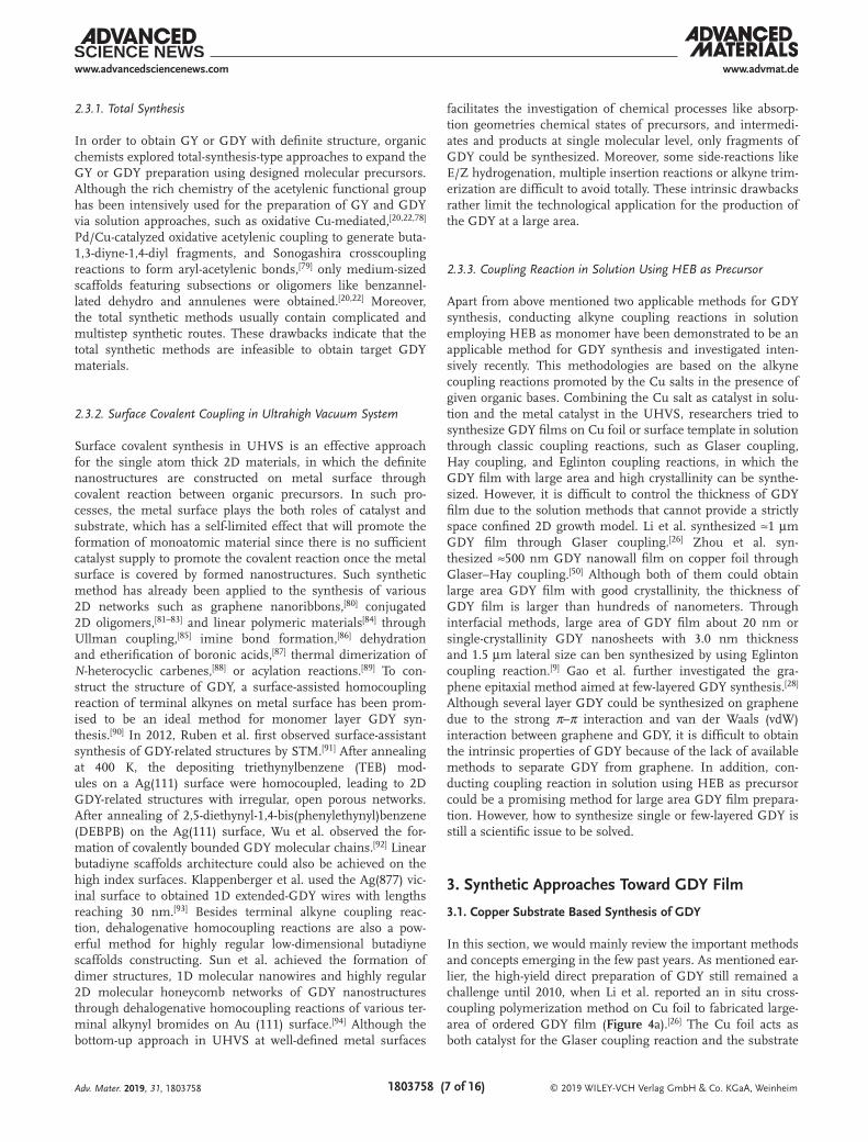
2.3. Common Synthetic Strategies
GDY was proposed to be a new 2D materials with many out-standing properties being predicted since it was first proposed, most of which are based on its few-layered 2D feature.[72–76] Therefore, developing reliable methods to produce high crystal-linity few-layered GDY with large domain size and investigating its intrinsic properties and potential applications are major goals. In order to prepare ultrathin 2D nanomaterials, scientist developed various reliable synthetic methods that can be divided into two categories: top-down and bottom-up methods. The top-down methods usually obtain thin layer 2D materials from their bulk crystals through exfoliating processes such as mechanical cleavage and liquid exfoliation. The bottom-up methods usually obtain thin layer 2D materials through chemical reactions of certain precursors at given experimental conditions. Chemical vapor deposition (CVD), surface covalent coupling in ultra-high vacuum system (UHVS), and wet-chemical syntheses are typical three kinds of bottom-up methods that are more versa-tile in principle comparing with top-down methods.[77] GDY is not existed in nature and its bulk crystals preparation methods are not available so far. Therefore, the top-down methods are not applicable for few-layered GDY preparation. Among the developed bottom-up approaches, three categories methods are proposed to be applicable to GDY preparation: total synthesis, surface covalent coupling in UHVS, and coupling reaction in solution using HEB as precursor (Figure 3).
Adv. Mater. 2019, 31, 1803758
Figure 3. Common synthetic strategies toward GDY.
© 2019 WILEY-VCH Verlag GmbH & Co. KGaA, Weinheim1803758 (7 of 16)
www.advmat.dewww.advancedsciencenews.com
2.3.1. Total Synthesis
In order to obtain GY or GDY with definite structure, organic chemists explored total-synthesis-type approaches to expand the GY or GDY preparation using designed molecular precursors. Although the rich chemistry of the acetylenic functional group has been intensively used for the preparation of GY and GDY via solution approaches, such as oxidative Cu-mediated,[20,22,78] Pd/Cu-catalyzed oxidative acetylenic coupling to generate buta-1,3-diyne-1,4-diyl fragments, and Sonogashira crosscoupling reactions to form aryl-acetylenic bonds,[79] only medium-sized scaffolds featuring subsections or oligomers like benzannel-lated dehydro and annulenes were obtained.[20,22] Moreover, the total synthetic methods usually contain complicated and multistep synthetic routes. These drawbacks indicate that the total synthetic methods are infeasible to obtain target GDY materials.
2.3.2. Surface Covalent Coupling in Ultrahigh Vacuum System
Surface covalent synthesis in UHVS is an effective approach for the single atom thick 2D materials, in which the definite nanostructures are constructed on metal surface through covalent reaction between organic precursors. In such pro-cesses, the metal surface plays the both roles of catalyst and substrate, which has a self-limited effect that will promote the formation of monoatomic material since there is no sufficient catalyst supply to promote the covalent reaction once the metal surface is covered by formed nanostructures. Such synthetic method has already been applied to the synthesis of various 2D networks such as graphene nanoribbons,[80] conjugated 2D oligomers,[81–83] and linear polymeric materials[84] through Ullman coupling,[85] imine bond formation,[86] dehydration and etherification of boronic acids,[87] thermal dimerization of N-heterocyclic carbenes,[88] or acylation reactions.[89] To con-struct the structure of GDY, a surface-assisted homocoupling reaction of terminal alkynes on metal surface has been prom-ised to be an ideal method for monomer layer GDY syn-thesis.[90] In 2012, Ruben et al. first observed surface-assistant synthesis of GDY-related structures by STM.[91] After annealing at 400 K, the depositing triethynylbenzene (TEB) mod-ules on a Ag(111) surface were homocoupled, leading to 2D GDY-related structures with irregular, open porous networks. After annealing of 2,5-diethynyl-1,4-bis(phenylethynyl)benzene (DEBPB) on the Ag(111) surface, Wu et al. observed the for-mation of covalently bounded GDY molecular chains.[92] Linear butadiyne scaffolds architecture could also be achieved on the high index surfaces. Klappenberger et al. used the Ag(877) vic-inal surface to obtained 1D extended-GDY wires with lengths reaching 30 nm.[93] Besides terminal alkyne coupling reac-tion, dehalogenative homocoupling reactions are also a pow-erful method for highly regular low-dimensional butadiyne scaffolds constructing. Sun et al. achieved the formation of dimer structures, 1D molecular nanowires and highly regular 2D molecular honeycomb networks of GDY nanostructures through dehalogenative homocoupling reactions of various ter-minal alkynyl bromides on Au (111) surface.[94] Although the bottom-up approach in UHVS at well-defined metal surfaces
facilitates the investigation of chemical processes like absorp-tion geometries chemical states of precursors, and intermedi-ates and products at single molecular level, only fragments of GDY could be synthesized. Moreover, some side-reactions like E/Z hydrogenation, multiple insertion reactions or alkyne trim-erization are difficult to avoid totally. These intrinsic drawbacks rather limit the technological application for the production of the GDY at a large area.
2.3.3. Coupling Reaction in Solution Using HEB as Precursor
Apart from above mentioned two applicable methods for GDY synthesis, conducting alkyne coupling reactions in solution employing HEB as monomer have been demonstrated to be an applicable method for GDY synthesis and investigated inten-sively recently. This methodologies are based on the alkyne coupling reactions promoted by the Cu salts in the presence of given organic bases. Combining the Cu salt as catalyst in solu-tion and the metal catalyst in the UHVS, researchers tried to synthesize GDY films on Cu foil or surface template in solution through classic coupling reactions, such as Glaser coupling, Hay coupling, and Eglinton coupling reactions, in which the GDY film with large area and high crystallinity can be synthe-sized. However, it is difficult to control the thickness of GDY film due to the solution methods that cannot provide a strictly space confined 2D growth model. Li et al. synthesized ≈1 µm GDY film through Glaser coupling.[26] Zhou et al. syn-thesized ≈500 nm GDY nanowall film on copper foil through Glaser–Hay coupling.[50] Although both of them could obtain large area GDY film with good crystallinity, the thickness of GDY film is larger than hundreds of nanometers. Through interfacial methods, large area of GDY film about 20 nm or single-crystallinity GDY nanosheets with 3.0 nm thickness and 1.5 µm lateral size can ben synthesized by using Eglinton coupling reaction.[9] Gao et al. further investigated the gra-phene epitaxial method aimed at few-layered GDY synthesis.[28] Although several layer GDY could be synthesized on graphene due to the strong π–π interaction and van der Waals (vdW) interaction between graphene and GDY, it is difficult to obtain the intrinsic properties of GDY because of the lack of available methods to separate GDY from graphene. In addition, con-ducting coupling reaction in solution using HEB as precursor could be a promising method for large area GDY film prepara-tion. However, how to synthesize single or few-layered GDY is still a scientific issue to be solved.
3. Synthetic Approaches Toward GDY Film
3.1. Copper Substrate Based Synthesis of GDY
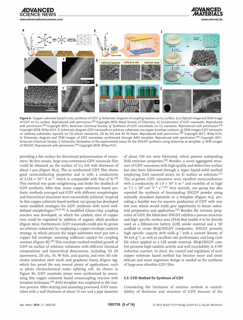
In this section, we would mainly review the important methods and concepts emerging in the few past years. As mentioned ear-lier, the high-yield direct preparation of GDY still remained a challenge until 2010, when Li et al. reported an in situ cross-coupling polymerization method on Cu foil to fabricated large-area of ordered GDY film (Figure 4a).[26] The Cu foil acts as both catalyst for the Glaser coupling reaction and the substrate
Adv. Mater. 2019, 31, 1803758
© 2019 WILEY-VCH Verlag GmbH & Co. KGaA, Weinheim1803758 (8 of 16)
www.advmat.dewww.advancedsciencenews.com
providing a flat surface for directional polymerization of mono-mers. By this means, large-area continuous GDY nanoscale film could be obtained on the surface of Cu foil with thickness of about 1 µm (Figure 4b,c). The as synthesized GDY film shows good semiconducting properties and is with a conductivity of 2.516 × 10⁻⁴ S m−1, which is comparable with that of Si.[26] This method was quite enlightening and broke the deadlock of GDY synthesis. After that, many copper substrates based syn-thetic methods emerged and GDY with different morphologies and hierarchical structures were successfully achieved. Inspired by this copper substrate based method, our group has developed some modified strategies for GDY synthesis with novel well-defined morphologies.[50,95,96] A modified Glaser–Hay coupling reaction was developed, in which the catalytic sites of copper ions could be regulated by addition of organic alkali pyridine (Figure 4d,e). Furthermore, GDY nanowalls could also be grown on arbitrary substrates by employing a copper envelope catalysis strategy, in which process the target substrates were put into a copper foil envelope, ensuring sufficient catalyst for coupling reaction (Figure 4f).[96] This envelope method enabled growth of GDY on surface of arbitrary substrates with different chemical compositions and hierarchical dimensions, including 1D (Si nanowires), 2D (Au, Ni, W foils, and quartz), and even 3D sub-strates (stainless steel mesh and graphene foam) (Figure 4g), which has paved the way toward plenty of applications, such as photo electrochemical water splitting cell. As shown in Figure 4h, GDY nanotube arrays were synthesized by associ-ating this copper substrate based crosscoupling reaction with template technique.[30] AAO template was employed in the reac-tion process. After etching and annealing processed, GDY nano-tubes with a wall thickness of about 15 nm and a pipe diameter
of about 150 nm were fabricated, which present outstanding field emission properties.[30] Besides, a novel aggregated struc-ture of GDY nanowires with high-quality and defect-free surface has also been fabricated through a vapor–liquid–solid method employing ZnO nanorod arrays on Si surface as substrate.[31] The as-grown GDY nanowires were excellent semiconductors with a conductivity of 1.9 × 10³ S m−1 and mobility of as high as 7.1 × 102 cm2 V−1 s−1.[31] Very recently, our group has also reported the synthesis of freestanding 3DGDY powder using naturally abundant diatomite as a template (Figure 4i,j), pro-viding a feasible way for massive production of GDY with very low cost, which would really give opportunity to future indus-trial preparation and application.[34] Besides the intrinsic prop-erties of GDY, the fabricated 3DGDY exhibits a porous structure and high specific surface area (SSA) that enable it to be directly used as a lithium-ion battery (LIB) anode material and a 3D scaffold to create Rh@3DGDY composites. 3DGDY presents high specific capacity (610 mAh g−1 with a current density of 50 mA g−1) as well as excellent rate performance and long cycle life when applied as a LIB anode material. Rh@3DGDY cata-lyst presents high catalytic activity and well recyclability in 4-NP reduction reaction. In short, the control and regulation of such copper substrate based method has become more and more delicate and more ingenious design is needed as for synthesis of large-area ultrathin GDY film.
3.2. CVD Method for Synthesis of GDY
Considering the limitation of solution method in control-lability of thickness and structure of GDY because of the
Adv. Mater. 2019, 31, 1803758
Figure 4. Copper substrate based in-situ synthesis of GDY. a) Schematic diagram of coupling reaction on Cu surface. b,c) Optical image and SEM image of GDY on Cu surface. Reproduced with permission.[26] Copyright 2010, Royal Society of Chemistry. d) Construction of GDY nanowalls. Reproduced with permission.[50] Copyright 2015, American Chemical Society. e) Synthesis of GDY nanosheets on Cu nanowire. Reproduced with permission.[33] Copyright 2018, Wiley-VCH. f) Schematic diagram GDY nanowalls on arbitrary substrates via copper envelope catalysis. g) SEM images GDY nanowalls on arbitrary substrates, typically on 1D silicon nanowires, 2D Au foil and 3D Ni foam. Reproduced with permission.[96] Copyright 2017, Wiley-VCH. h) Schematic diagram and TEM images of GDY nanotubes synthesized through AAO template. Reproduced with permission.[30] Copyright 2011, American Chemical Society. i) Schematic illustration of the experimental setup for the 3DGDY synthesis using diatomite as template. j) SEM images of 3DGDY. Reproduced with permission.[34] Copyright 2018, Wiley-VCH.
© 2019 WILEY-VCH Verlag GmbH & Co. KGaA, Weinheim1803758 (9 of 16)
www.advmat.dewww.advancedsciencenews.com
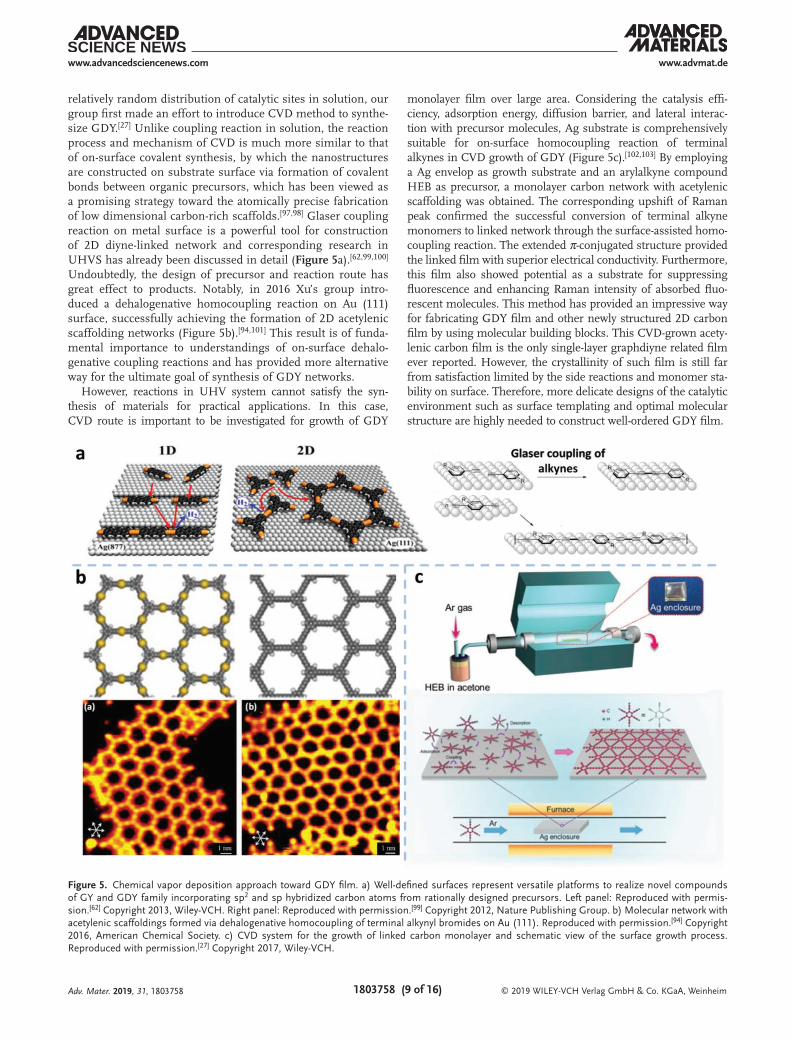
relatively random distribution of catalytic sites in solution, our group first made an effort to introduce CVD method to synthe-size GDY.[27] Unlike coupling reaction in solution, the reaction process and mechanism of CVD is much more similar to that of on-surface covalent synthesis, by which the nanostructures are constructed on substrate surface via formation of covalent bonds between organic precursors, which has been viewed as a promising strategy toward the atomically precise fabrication of low dimensional carbon-rich scaffolds.[97,98] Glaser coupling reaction on metal surface is a powerful tool for construction of 2D diyne-linked network and corresponding research in UHVS has already been discussed in detail (Figure 5a).[62,99,100] Undoubtedly, the design of precursor and reaction route has great effect to products. Notably, in 2016 Xu’s group intro-duced a dehalogenative homocoupling reaction on Au (111) surface, successfully achieving the formation of 2D acetylenic scaffolding networks (Figure 5b).[94,101] This result is of funda-mental importance to understandings of on-surface dehalo-genative coupling reactions and has provided more alternative way for the ultimate goal of synthesis of GDY networks.
However, reactions in UHV system cannot satisfy the syn-thesis of materials for practical applications. In this case, CVD route is important to be investigated for growth of GDY
monolayer film over large area. Considering the catalysis effi-ciency, adsorption energy, diffusion barrier, and lateral interac-tion with precursor molecules, Ag substrate is comprehensively suitable for on-surface homocoupling reaction of terminal alkynes in CVD growth of GDY (Figure 5c).[102,103] By employing a Ag envelop as growth substrate and an arylalkyne compound HEB as precursor, a monolayer carbon network with acetylenic scaffolding was obtained. The corresponding upshift of Raman peak confirmed the successful conversion of terminal alkyne monomers to linked network through the surface-assisted homo-coupling reaction. The extended π-conjugated structure provided the linked film with superior electrical conductivity. Furthermore, this film also showed potential as a substrate for suppressing fluorescence and enhancing Raman intensity of absorbed fluo-rescent molecules. This method has provided an impressive way for fabricating GDY film and other newly structured 2D carbon film by using molecular building blocks. This CVD-grown acety-lenic carbon film is the only single-layer graphdiyne related film ever reported. However, the crystallinity of such film is still far from satisfaction limited by the side reactions and monomer sta-bility on surface. Therefore, more delicate designs of the catalytic environment such as surface templating and optimal molecular structure are highly needed to construct well-ordered GDY film.
Adv. Mater. 2019, 31, 1803758
Figure 5. Chemical vapor deposition approach toward GDY film. a) Well-defined surfaces represent versatile platforms to realize novel compounds of GY and GDY family incorporating sp2 and sp hybridized carbon atoms from rationally designed precursors. Left panel: Reproduced with permis-sion.[62] Copyright 2013, Wiley-VCH. Right panel: Reproduced with permission.[99] Copyright 2012, Nature Publishing Group. b) Molecular network with acetylenic scaffoldings formed via dehalogenative homocoupling of terminal alkynyl bromides on Au (111). Reproduced with permission.[94] Copyright 2016, American Chemical Society. c) CVD system for the growth of linked carbon monolayer and schematic view of the surface growth process. Reproduced with permission.[27] Copyright 2017, Wiley-VCH.
© 2019 WILEY-VCH Verlag GmbH & Co. KGaA, Weinheim1803758 (10 of 16)
www.advmat.dewww.advancedsciencenews.com
3.3. Interfacial Construction for the Synthesis of GDY
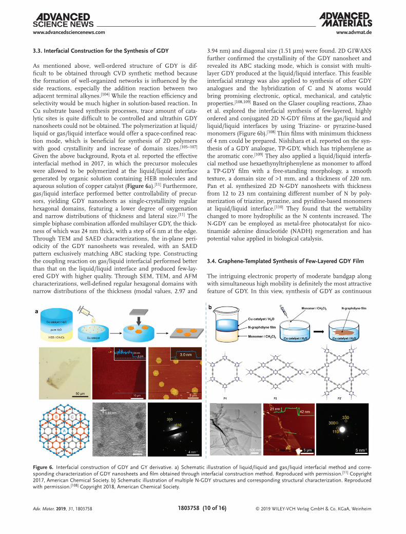
As mentioned above, well-ordered structure of GDY is dif-ficult to be obtained through CVD synthetic method because the formation of well-organized networks is influenced by the side reactions, especially the addition reaction between two adjacent terminal alkynes.[104] While the reaction efficiency and selectivity would be much higher in solution-based reaction. In Cu substrate based synthesis processes, trace amount of cata-lytic sites is quite difficult to be controlled and ultrathin GDY nanosheets could not be obtained. The polymerization at liquid/liquid or gas/liquid interface would offer a space-confined reac-tion mode, which is beneficial for synthesis of 2D polymers with good crystallinity and increase of domain sizes.[105–107] Given the above background, Ryota et al. reported the effective interfacial method in 2017, in which the precursor molecules were allowed to be polymerized at the liquid/liquid interface generated by organic solution containing HEB molecules and aqueous solution of copper catalyst (Figure 6a).[11] Furthermore, gas/liquid interface performed better controllability of precur-sors, yielding GDY nanosheets as single-crystallinity regular hexagonal domains, featuring a lower degree of oxygenation and narrow distributions of thickness and lateral size.[11] The simple biphase combination afforded multilayer GDY, the thick-ness of which was 24 nm thick, with a step of 6 nm at the edge. Through TEM and SAED characterizations, the in-plane peri-odicity of the GDY nanosheets was revealed, with an SAED pattern exclusively matching ABC stacking type. Constructing the coupling reaction on gas/liquid interfacial performed better than that on the liquid/liquid interface and produced few-lay-ered GDY with higher quality. Through SEM, TEM, and AFM characterizations, well-defined regular hexagonal domains with narrow distributions of the thickness (modal values, 2.97 and
3.94 nm) and diagonal size (1.51 µm) were found. 2D GIWAXS further confirmed the crystallinity of the GDY nanosheet and revealed its ABC stacking mode, which is consist with multi-layer GDY produced at the liquid/liquid interface. This feasible interfacial strategy was also applied to synthesis of other GDY analogues and the hybridization of C and N atoms would bring promising electronic, optical, mechanical, and catalytic properties.[108,109] Based on the Glaser coupling reactions, Zhao et al. explored the interfacial synthesis of few-layered, highly ordered and conjugated 2D N-GDY films at the gas/liquid and liquid/liquid interfaces by using Triazine- or pyrazine-based monomers (Figure 6b).[108] Thin films with minimum thickness of 4 nm could be prepared. Nishihara et al. reported on the syn-thesis of a GDY analogue, TP-GDY, which has triphenylene as the aromatic core.[109] They also applied a liquid/liquid interfa-cial method use hexaethynyltriphenylene as monomer to afford a TP-GDY film with a free-standing morphology, a smooth texture, a domain size of >1 mm, and a thickness of 220 nm. Pan et al. synthesized 2D N-GDY nanosheets with thickness from 12 to 23 nm containing different number of N by poly-merization of triazine, pyrazine, and pyridine-based monomers at liquid/liquid interface.[110] They found that the wettability changed to more hydrophilic as the N contents increased. The N-GDY can be employed as metal-free photocatalyst for nico-tinamide adenine dinucleotide (NADH) regeneration and has potential value applied in biological catalysis.
3.4. Graphene-Templated Synthesis of Few-Layered GDY Film
The intriguing electronic property of moderate bandgap along with simultaneous high mobility is definitely the most attractive feature of GDY. In this view, synthesis of GDY as continuous
Adv. Mater. 2019, 31, 1803758
Figure 6. Interfacial construction of GDY and GY derivative. a) Schematic illustration of liquid/liquid and gas/liquid interfacial method and corre-sponding characterization of GDY nanosheets and film obtained through interfacial construction method. Reproduced with permission.[11] Copyright 2017, American Chemical Society. b) Schematic illustration of multiple N-GDY structures and corresponding structural characterization. Reproduced with permission.[108] Copyright 2018, American Chemical Society.
© 2019 WILEY-VCH Verlag GmbH & Co. KGaA, Weinheim1803758 (11 of 16)
www.advmat.dewww.advancedsciencenews.com
ultrathin film capable of in-plane charge transport is highly demanded for better fulfillment of the electronic devices practi-cally. Besides, the formation of thin film would be much more beneficial for fine structural characterization.
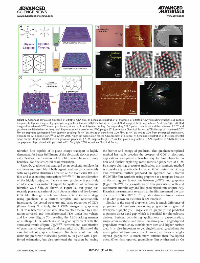
Recently, graphene has emerged as an excellent template for synthesis and assembly of both organic and inorganic materials with well-packed structures because of the atomically flat sur-face and π–π stacking interactions.[65,66,112–114] In consideration of the highly conjugated flat structure, graphene is positively an ideal choice as surface template for synthesis of continuous ultrathin GDY film. As shown in Figure 7a, our group has recently presented series of work about synthesis of few-layered GDY film through a solution phase vdW epitaxial strategy using graphene as a surface template and systematically investigated the crystal structure and basic properties of GDY (Figure 7b–e).[29] Notably, the HRTEM images of graphene/GDY vdW heterostructure were also directly observed by a ber-ration-corrected and monochromated TEM under low voltage and low dose (Figure 7f), revealing the ABC-stacking manner of multilayer GDY, which is also in good agreement with the simulated result (Figure 7g).[28,29] Furthermore, combination of experimental observation and theoretical also illustrated the essential role of graphene template. Graphene would not only make the precursor molecules parallel to its plane with a pre-ferred orientation, but also promoted the reaction by lowing
the barrier and energy of products. This graphene-templated method has really broaden the prospect of GDY in electronic applications and paved a feasible way for fine characteriza-tion and further exploring more intrinsic properties of GDY. By simple altering precursor molecules, this synthetic method is considerably practicable for other GDY derivatives. Zhang and coworkers further proposed an approach for ultrathin β-GDY-like film synthesis using graphene as a template because of the strong π-π interaction between β-GDY and graphene (Figure 7h).[111] The as-synthesized film presents smooth and continuous morphology and has good crystallinity (Figure 7i,j). Electrical measurement reveals that the film presented the con-ductivity of 1.30 × 10⁻² S m−1 by fabricating electronic devices on β-GDY grown on dielectric h-BN template.
Similar to the case of graphene, there is much difference of properties and synthesis developing progress for single- and few-layered graphdiyne. Single-layered graphdiyne is predicted to possess direct band gap, which is beneficial for photoelectric devices. Besides, considering applications in gas-separation, single-atom catalysis, and metal ion absorption, single-layered graphdiyne would show suitable pore size and higher surface area. It is also important to get single-layered graphdiyne for investigation of basic properties. However, synthesis of single-layered graphdiyne is much more difficult than few-layered ones. When first reported, graphdiyne film synthesized on Cu
Adv. Mater. 2019, 31, 1803758
Figure 7. Graphene-templated synthesis of ultrathin GDY film. a) Schematic illustration of synthesis of ultrathin GDY film using graphene as surface template. b) Optical images of graphdiyne on graphene film on SiO2/Si substrate. c) Typical AFM image of GDY on graphene. Scale bar, 5 µm. d) TEM image of transferred GDY film on graphene synthesized from Hiyama coupling. Corresponding SEAD pattern is in inset and the patterns of GDY and graphene are labelled respectively. a–d) Reproduced with permission.[29] Copyright 2018, American Chemical Society. e) TEM image of transferred GDY film on graphene synthesized from Eglinton coupling. f) HRTEM image of transferred GDY film. g) HRTEM image GDY from theoretical predication. Reproduced with permission.[28] Copyright 2018, American Association for the Advancement of Science. h) Schematic illustration of the experimental setup for the ultrathin β-GDY-like film grown on graphene. i) AFM image of the β-GDY-like film grown on graphene. j) SAED pattern of β-GDY-like film on graphene. Reproduced with permission.[111] Copyright 2018, American Chemical Society.
© 2019 WILEY-VCH Verlag GmbH & Co. KGaA, Weinheim1803758 (12 of 16)
www.advmat.dewww.advancedsciencenews.com
surface turned out to be 1 µm.[26] By controlling the concen-tration of Cu catalysis, utilizing the gas/liquid–liquid interface, and employing graphene as a surface template, the morphology and thickness of graphdiyne were well regulated. Up to now, few-layered graphdiyne was successfully obtained with thick-ness less than 2 nm and the stacking manner was identified systematically.[28] The achievement in fewer-layered graphdiyne synthesis would contribute a lot to the application in electronic properties investigation and optical research. CVD method is really competitive for single-layered growth while there is still a far way for improving the film crystallinity. We can see that great progress has been made for thickness control and crystallinity improvement.
4. Raman Spectroscopy of GDY
As for such a new-born material, efficient characterization methods are highly requisite providing beneficial guidance for improvement of synthetic methods. In the history of carbon materials, Raman spectroscopy has played a crucial role and the positions, intensities and shapes of Raman bands can offer rich helpful information.[115,116] It is also a powerful tool for the investigation of Raman-active CC triple bond. Our group has done much work in the study of Raman spectroscopy of GDY related system with combination of experimental results and theoretical simulations, gaining deeper insight into the crystal-linity structure, defect degree and reaction mechanism.[71,117] Raman spectroscopy has also made much contribution for the development of GDY synthesis and a scientific characterization method has been built up gradually.
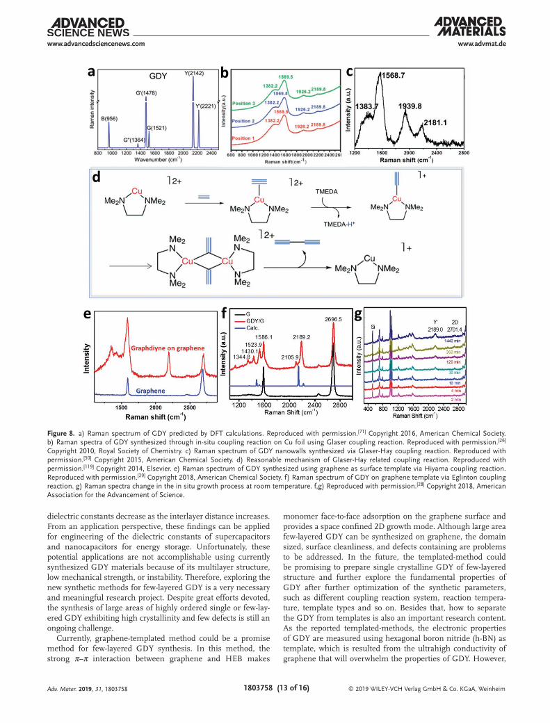
Raman peaks and corresponding lattice vibrational modes are specified. Typically, there are six intense Raman peaks of GDY shown in Figure 8a, falling into three categories: B band coming from breathing vibration; G, G′, and G″ bands related to sp2 carbon and Y, Y′ bands for alkyne-related modes, respec-tively.[71,117] To be more specific, the B peak at 956 cm−1 mainly comes from breathing vibration of benzene rings and alkyne-related rings. G peak at around 1520 cm−1 can be attributed to the stretching of aromatic rings similar to G peak of graphene. However, the G peak of GDY has a bathochromic-shift and lower intensity than that of graphene, suggesting the introduc-tion of acetylenic linkages into this alkyne-rich system. G′ peak comes from vibration of CC bonds between triply coordinated atoms and their doubly coordinated neighbors; G″ peak can be ascribed to the scissoring vibration of atoms in benzene rings; Y and Y′ peaks are both stretching modes of triple bonds with the difference that Y refers to in-phase synchronous contrac-tion stretching of triple bonds which is a fully symmetric mode, while Y′ comes from out-of-phase stretching.[71]
Raman spectroscopy can also provide abundant informa-tion about reaction process and mechanism. Interestingly, an unexpected peak often appeared at around 1940 cm−1 and was assigned to some vibration related to C–Cu (II) complex, which is an intermediate of alkyne homocoupling reaction and could be easily understood from the mechanism of alkyne cou-pling reaction. As shown in Figure 8b,c, in the Raman spectra of GDY with higher thickness, the peak of C–Cu (II) complex would be obvious because the lack of oxidant for completing
spsp bond formation. In most Cu-catalyzed terminal alkynes coupling reactions, one of the most elaborated proposals can be explicated in Figure 8d. The reaction starts with π-coordination of the triple bond to copper (I) catalyst facilitating the activa-tion of their terminal CH bond by an external base. After the formation of a dinuclear specie, diyne bonds would form by reductive elimination from dinuclear specie in the presence of oxidant.[118–120] While as for graphene-templated synthesis of ultrathin GDY film, the intermediate peak disappeared totally (Figure 8e,f), indicating better coupling efficiency.[29] Raman spectroscopy is also beneficial for monitoring the reaction pro-cess. In situ Raman spectroscopy of Y′ peak was conducted and the evolution process is shown in Figure 8g.[29] Y′ peak would appear in a short reaction time (<4 min), indicating a rapid rate at the initial stage and as time extended, the intensity of Y′ peak showed a significant enhancement, indicating the continuing coupling reaction of terminal alkynes. Furthermore, with reac-tion time increasing, the reaction rate would decrease because of the lower solubility and reactivity of the enlarged networks.
The progress of GDY synthesis has provided better condi-tions for investigation of related Raman spectroscopy. And in return, better understanding of the reaction process and mech-anism would also be much beneficial for experimental design and optimizing conditions. The study of GDY Raman spectros-copy has contributed a lot for improving of synthetic strategies.
5. Summary and Outlook
GDY, a new type of carbon allotrope, has attracted widespread attention since it is first proposed. Since Li and co-workers successfully synthesized large area of GDY nanoscale film on copper substrate, GDY has showed potential applications in many fields. Meanwhile, some other modified methods were developed to synthesize GDY with different morphologies, which greatly enriched the synthetic methods and application fields of GDY. However, the synthesis of single or few layer GDY with well-defined structure and large domain sized is still infancy and is an unswerving pursuit of the goal for scientists. One the one hand, the few-layered GDY is the study basic of intrinsic properties, such as mechanical, band, electronic, and thermal properties. However, the basic study of intrinsic properties has been developing slowly subjecting to the syn-thetic methods that cannot synthesize the desired GDY mate-rial. On the other hand, few-layered GDY could display bright applications in other areas (e.g., dielectric screening and gas separation).[37,121] The framework of GDY is constructed by hexagonal carbon rings cross linked by diacetylenic linkages. The size of vdW pores defined by the framework is in between hydrogen and CH4/CO, and makes GDY possible to be utilized as a selective separation membrane for hydrogen purification from syngas.[13,17] Further study revealed that GDY is an ideal membrane to separate O2 from harmful gases like Cl2, HCl, HCN, CNCl, SO2, H2S, NH3, and CH2O.[122] Based on the DFT calculations, Lee et al. found that few-layered GDY and its family could be an ideal material applied an off-plane, static dielectric screening, in which the vertical dielectric constants of GDY independent of the thickness, while those of metallic materials are dependent on the thickness.[121] Furthermore, the
Adv. Mater. 2019, 31, 1803758
© 2019 WILEY-VCH Verlag GmbH & Co. KGaA, Weinheim1803758 (13 of 16)
www.advmat.dewww.advancedsciencenews.com
Adv. Mater. 2019, 31, 1803758
dielectric constants decrease as the interlayer distance increases. From an application perspective, these findings can be applied for engineering of the dielectric constants of supercapacitors and nanocapacitors for energy storage. Unfortunately, these potential applications are not accomplishable using currently synthesized GDY materials because of its multilayer structure, low mechanical strength, or instability. Therefore, exploring the new synthetic methods for few-layered GDY is a very necessary and meaningful research project. Despite great efforts devoted, the synthesis of large areas of highly ordered single or few-lay-ered GDY exhibiting high crystallinity and few defects is still an ongoing challenge.
Currently, graphene-templated method could be a promise method for few-layered GDY synthesis. In this method, the strong π–π interaction between graphene and HEB makes
monomer face-to-face adsorption on the graphene surface and provides a space confined 2D growth mode. Although large area few-layered GDY can be synthesized on graphene, the domain sized, surface cleanliness, and defects containing are problems to be addressed. In the future, the templated-method could be promising to prepare single crystalline GDY of few-layered structure and further explore the fundamental properties of GDY after further optimization of the synthetic parameters, such as different coupling reaction system, reaction tempera-ture, template types and so on. Besides that, how to separate the GDY from templates is also an important research content. As the reported templated-methods, the electronic properties of GDY are measured using hexagonal boron nitride (h-BN) as template, which is resulted from the ultrahigh conductivity of graphene that will overwhelm the properties of GDY. However,
Figure 8. a) Raman spectrum of GDY predicted by DFT calculations. Reproduced with permission.[71] Copyright 2016, American Chemical Society. b) Raman spectra of GDY synthesized through in-situ coupling reaction on Cu foil using Glaser coupling reaction. Reproduced with permission.[26] Copyright 2010, Royal Society of Chemistry. c) Raman spectrum of GDY nanowalls synthesized via Glaser-Hay coupling reaction. Reproduced with permission.[50] Copyright 2015, American Chemical Society. d) Reasonable mechanism of Glaser-Hay related coupling reaction. Reproduced with permission.[119] Copyright 2014, Elsevier. e) Raman spectrum of GDY synthesized using graphene as surface template via Hiyama coupling reaction. Reproduced with permission.[29] Copyright 2018, American Chemical Society. f) Raman spectrum of GDY on graphene template via Eglinton coupling reaction. g) Raman spectra change in the in situ growth process at room temperature. f,g) Reproduced with permission.[28] Copyright 2018, American Association for the Advancement of Science.
© 2019 WILEY-VCH Verlag GmbH & Co. KGaA, Weinheim1803758 (14 of 16)
www.advmat.dewww.advancedsciencenews.com
Adv. Mater. 2019, 31, 1803758
the quality of GDY growth on h-BN is not as high as on gra-phene due to the weak interaction between h-BN and GDY. Therefore, better results should be obtained if the electronic properties can be measured on GDY films that are exfoliated from graphene.
GDY represents an important novel class of 2D carbon mate-rials with a multitude of appealing properties, all the challenge will certainly be overcome in near future addressing a lot of novel interesting materials properties. However, there is still a long way to make actually become an irreplaceable material in the future and need scientific research workers to make more hard efforts.
AcknowledgementsThis article is part of a special section on graphdiyne. J.Z. and J.L. contributed equally to this work. This work was supported by the Ministry of Science and Technology of China (2016YFA0200101 and 2016YFA0200104), National Natural Science Foundation of China (51432002, 51720105003, and 21790052), and Beijing Municipal Science and Technology Project (161100002116026).
Conflict of InterestThe authors declare no conflict of interest.
Keywordsgraphdiyne, graphene template, in situ coupling reaction, interfacial construction, synthetic strategy
Received: June 13, 2018Revised: December 29, 2018
Published online: February 18, 2019
[1] A. Hirsch, Nat. Mater. 2010, 9, 868.[2] J. Zhang, M. Terrones, C. R. Park, R. Mukherjee, M. Monthioux,
N. Koratkar, Y. S. Kim, R. Hurt, E. Frackowiak, T. Enoki, Carbon 2016, 98, 708.
[3] M. Long, L. Tang, D. Wang, Y. Li, Z. Shuai, ACS Nano 2011, 5, 2593.[4] A. R. Puigdollers, G. Alonso, P. Gamallo, Carbon 2016, 96, 879.[5] M. M. Haley, S. C. Brand, J. J. Pak, Angew. Chem., Int. Ed. Engl.
1997, 36, 836.[6] N. Narita, S. Nagai, S. Suzuki, K. Nakao, Phys. Rev. B 1998, 58,
11009.[7] G. Luo, X. Qian, H. Liu, R. Qin, J. Zhou, L. Li, Z. Gao, E. Wang,
W. Mei, J. Lu, Y. Li, S. Nagase, Phys. Rev. B 2011, 84, 075439.[8] S. W. Cranford, M. J. Buehler, Carbon 2011, 49, 4111.[9] Q. Zheng, G. Luo, Q. Liu, R. Quhe, J. Zheng, K. Tang, Z. Gao,
S. Nagase, J. Lu, Nanoscale 2012, 4, 3990.[10] C. Li, X. Lu, Y. Han, S. Tang, Y. Ding, R. Liu, H. Bao, Y. Li, J. Luo,
T. Lu, Nano Res. 2018, 11, 1714.[11] R. Matsuoka, R. Sakamoto, K. Hoshiko, S. Sasaki, H. Masunaga,
K. Nagashio, H. Nishihara, J. Am. Chem. Soc. 2017, 139, 3145.[12] H. Cui, X. Sheng, Q. Yan, Q. Zheng, G. Su, Phys. Chem.
Chem. Phys. 2013, 15, 8179.[13] Y. Jiao, A. Du, M. Hankel, Z. Zhu, V. Rudolph, S. C. Smith,
Chem. Commun. 2011, 47, 11843.
[14] L. Sun, P. Jiang, H. Liu, D. Fan, J. Liang, J. Wei, L. Cheng, J. Zhang, J. Shi, Carbon 2015, 90, 255.
[15] C. Huang, S. Zhang, H. Liu, Y. Li, G. Cui, Y. Li, Nano Energy 2015, 11, 481.
[16] J. Li, X. Gao, X. Jiang, X. Li, Z. Liu, J. Zhang, C. Tung, L. Wu, ACS Catal. 2017, 7, 5209.
[17] S. W. Cranford, M. J. Buehler, Nanoscale 2012, 4, 4587.[18] A. Bhaskar, R. Guda, M. M. Haley, Goodson, J. Am. Chem. Soc.
2006, 128, 13972.[19] F. Diederich, M. Kivala, Adv. Mater. 2010, 22, 803.[20] J. J. Pak, T. J. R. Weakley, M. M. Haley, J. Am. Chem. Soc. 1999, 121,
8182.[21] M. M. Haley, Pure Appl. Chem. 2008, 80, 519.[22] U. H. F. Bunz, Y. Rubin, Y. Tobe, Chem. Soc. Rev. 1999, 28, 107.[23] S. Anand, O. Varnavski, J. A. Marsden, M. M. Haley, H. B. Schlegel,
T. Goodson, J. Phys. Chem. A 2006, 110, 1305.[24] J. A. Marsden, M. M. Haley, J. Org. Chem. 2005, 70, 10213.[25] G. Li, Y. Li, H. Liu, Y. Guo, Y. Li, D. Zhu, Chem. Commun. 2010, 46,
3256.[26] R. Liu, X. Gao, J. Zhou, H. Xu, Z. Li, S. Zhang, Z. Xie, J. Zhang,
Z. Liu, Adv. Mater. 2017, 29, 1604665.[27] X. Gao, Y. Zhu, D. Yi, J. Zhou, S. Zhang, C. Yin, F. Ding, S. Zhang,
X. Yi, J. Wang, L. Tong, Y. Han, Z. Liu, J. Zhang, Sci. Adv. 2018, 4, eaat6378.
[28] J. Zhou, Z. Xie, R. Liu, X. Gao, J. Li, Y. Xiong, L. Tong, J. Zhang, Z. Liu, ACS Appl. Mater. Interfaces 2018, https://doi.org/10.1021/acsami.8b02612.
[29] G. Li, Y. Li, X. Qian, H. Liu, H. Lin, N. Chen, Y. Li, J. Phys. Chem. C 2011, 115, 2611.
[30] X. Qian, Z. Ning, Y. Li, H. Liu, C. Ouyang, Q. Chen, Y. Li, Dalton Trans. 2012, 41, 730.
[31] Y. Xue, Y. Guo, Y. Yi, Y. Li, H. Liu, D. Li, W. Yang, Y. Li, Nano Energy 2016, 30, 858.
[32] H. Shang, Z. Zuo, L. Li, F. Wang, H. Liu, Y. Li, Y. Li, Angew. Chem., Int. Ed. 2018, 57, 774.
[33] J. Li, J. Xu, Z. Xie, X. Gao, J. Zhou, Y. Xiong, C. Chen, J. Zhang, Z. Liu, Adv. Mater. 2018, 30, 1800548.
[34] C. Huang, Y. Li, Acta Phys. Chim. Sin. 2016, 32, 1314.[35] Y. Chen, H. Liu, Y. Li, Chin. Sci. Bull. 2016, 61, 2901.[36] J. Kang, Z. Wei, J. Li, ACS Appl. Mater. Interfaces 2018, https://doi.
org/10.1021/acsami.8b03338.[37] Y. Li, L. Xu, H. Liu, Y. Li, Chem. Soc. Rev. 2014, 43, 2572.[38] H. W. Kroto, J. R. Heath, S. C. Obrien, R. F. Curl, R. E. Smalley,
Nature 1985, 318, 162.[39] S. Iijima, Nature 1991, 354, 56.[40] K. S. Novoselov, A. K. Geim, S. V. Morozov, D. Jiang, Y. Zhang,
S. V. Dubonos, I. V. Grigorieva, A. A. Firsov, Science 2004, 306, 666.
[41] X. Chen, Z. Chen, W. Jiang, C. Zhang, J. Sun, H. Wang, W. Xin, L. Lin, M. K. Priydarshi, H. Yang, Z. Liu, J. Tian, Y. Zhang, Y. Zhang, Z. Liu, Adv. Mater. 2017, 29, 1603428.
[42] D. Geng, H. Wang, G. Yu, Adv. Mater. 2015, 27, 2821.[43] H. Kim, I. Song, C. Park, M. Son, M. Hong, Y. Kim, J. S. Kim,
H.-J. Shin, J. Baik, H. C. Choi, ACS Nano 2013, 7, 6575.[44] S. Lee, K. Lee, Z. Zhong, Nano Lett. 2010, 10, 4702.[45] L. Hu, X. Hu, X. Wu, C. Du, Y. Dai, J. Deng, Phys. B 2010, 405,
3337.[46] K. T. Chan, J. B. Neaton, M. L. Cohen, Phys. Rev. B 2008, 77,
235430.[47] S. Wang, L. Yi, J. E. Halpert, X. Lai, Y. Liu, H. Cao, R. Yu, D. Wang,
Y. Li, Small 2012, 8, 265.[48] S. Zhang, H. Liu, C. Huang, G. Cui, Y. Li, Chem. Commun. 2015,
51, 1834.[49] J. Zhou, X. Gao, R. Liu, Z. Xie, J. Yang, S. Zhang, G. Zhang, H. Liu,
Y. Li, J. Zhang, Z. Liu, J. Am. Chem. Soc. 2015, 137, 7596.
© 2019 WILEY-VCH Verlag GmbH & Co. KGaA, Weinheim1803758 (15 of 16)
www.advmat.dewww.advancedsciencenews.com
Adv. Mater. 2019, 31, 1803758
[50] H. Shang, Z. Zuo, L. Li, F. Wang, H. Liu, Y. Li, Y. Li, Angew. Chem. Int. Ed. 2018. 130, 782.
[51] S. Wang, H. Liu, X. Kan, L. Wang, Y. Chen, B. Su, Y. Li, L. Jiang, Small 2017, 13, 1602265.
[52] H. Lindlar, R. Dubuis, Org. Synth. 1966, 46, 89.[53] Y. Angell, K. Burgess, Angew. Chem., Int. Ed. 2007, 46, 3649.[54] P. Leophairatana, S. Samanta, C. C. De Silva, J. T. Koberstein,
J. Am. Chem. Soc. 2017, 139, 3756.[55] S. Lee, E. Chenard, D. L. Gray, J. S. Moore, J. Am. Chem. Soc. 2016,
138, 13814.[56] R. Du, N. Zhang, H. Xu, N. Mao, W. Duan, J. Wang, Q. Zhao,
Z. Liu, J. Zhang, Adv. Mater. 2014, 26, 8053.[57] L. Blanco, H. E. Helson, M. Hirthammer, H. Mestdagh,
S. Spyroudis, K. P. C. Vollhardt, Angew. Chem. 1987, 99, 1276.
[58] R. Diercks, J. C. Armstrong, R. Boese, K. P. C. Vollhardt, Angew. Chem., Int. Ed. Engl. 1986, 25, 268.
[59] J. Chandrasekhar, E. D. Jemmis, P. v. R. Schleyer, Tetrahedron Lett. 1979, 20, 3707.
[60] R. Chinchilla, C. Najera, Chem. Rev. 2014, 114, 1783.[61] A. S. Batsanov, J. C. Collings, I. J. S. Fairlamb, J. P. Holland,
J. A. K. Howard, Z. Lin, T. B. Marder, A. C. Parsons, R. M. Ward, J. Zhu, J. Org. Chem. 2005, 70, 703.
[62] H. Gao, H. Wagner, D. Zhong, J. H. Franke, A. Studer, H. Fuchs, Angew. Chem., Int. Ed. 2013, 52, 4024.
[63] J. Sakamoto, J. V. Heijst, O. Lukin, A. D. Schluter, Angew. Chem., Int. Ed. 2009, 48, 1030.
[64] L. Xu, X. Zhou, W. Tian, T. Gao, Y. Zhang, S. Lei, Z. Liu, Angew. Chem., Int. Ed. 2014, 53, 9564.
[65] K. Kim, E. J. G. Santos, T. H. Lee, Y. Nishi, Z. Bao, Small 2015, 11, 2037.
[66] J. W. Colson, A. R. Woll, A. Mukherjee, M. P. Levendorf, E. L. Spitler, V. B. Shields, M. G. Spencer, J. Park, W. R. Dichtel, Science 2011, 332, 228.
[67] A. C. Ferrari, D. M. Basko, Nat. Nanotechnol. 2013, 8, 235.[68] S. B. Cronin, A. K. Swan, M. S. Ünlü, B. B. Goldberg,
M. S. Dresselhaus, M. Tinkham, Phys. Rev. Lett. 2004, 93, 167401.
[69] J. Wu, H. Xu, J. Zhang, Acta Chim. Sin. 2014, 72, 301.[70] Y. Wang, Z. Ni, Z. Shen, H. Wang, Y. Wu, Appl. Phys. Lett. 2008, 92,
043121.[71] S. Zhang, J. Wang, Z. Li, R. Zhao, L. Tong, Z. Liu, J. Zhang, Z. Liu,
J. Phys. Chem. C 2016, 120, 10605.[72] Z. Lu, S. Li, P. Lv, C. He, D. Ma, Z. Yang, Appl. Surf. Sci. 2016, 360,
1.[73] L. Pan, L. Zhang, B. Song, S. Du, H. Gao, Appl. Phys. Lett. 2011,
98, 173102.[74] K. Srinivasu, S. K. Ghosh, J. Phys. Chem. C 2012, 116, 5951.[75] C. Sun, D. J. Searles, J. Phys. Chem. C 2012, 116, 26222.[76] Y. Zheng, Y. Chen, L. Lin, Y. Sun, H. Liu, Y. Li, Y. Du, N. Tang,
Appl. Phys. Lett. 2017, 111, 033101.[77] C. Tan, X. Cao, X. Wu, Q. He, J. Yang, X. Zhang, J. Chen, W. Zhao,
S. Han, G. H. Nam, M. Sindoro, H. Zhang, Chem. Rev. 2017, 117, 6225.
[78] F. Klappenberger, Y. Zhang, J. Bjork, S. Klyatskaya, M. Ruben, J. V. Barth, Acc. Chem. Res. 2015, 48, 2140.
[79] I. J. S. Fairlamb, P. S. Bäuerlein, L. R. Marrison, J. M. Dickinson, Chem. Commun. 2003, 632.
[80] J. Cai, P. Ruffieux, R. Jaafar, M. Bieri, T. Braun, S. Blankenburg, M. Muoth, A. P. Seitsonen, M. Saleh, X. Feng, K. Mullen, R. Fasel, Nature 2010, 466, 470.
[81] D. F. Perepichka, F. Rosei, Science 2009, 323, 216.[82] M. Bieri, S. Blankenburg, M. Kivala, C. A. Pignedoli, P. Ruffieux,
K. Mullen, R. Fasel, Chem. Commun. 2011, 47, 10239.
[83] Z. Yang, J. Gebhardt, T. A. Schaub, T. Sander, J. Schönamsgruber, H. Soni, A. Görling, M. Kivala, S. Maier, Nanoscale 2018, 10, 3769.
[84] L. Lafferentz, F. Ample, H. Yu, S. Hecht, C. Joachim, L. Grill, Science 2009, 323, 1193.
[85] L. Lafferentz, V. Eberhardt, C. Dri, C. Africh, G. Comelli, F. Esch, S. Hecht, L. Grill, Nat. Chem. 2012, 4, 215.
[86] S. Weigelt, C. Busse, C. Bombis, M. M. Knudsen, K. V. Gothelf, T. Strunskus, C. Wöll, M. Dahlbom, B. Hammer, E. Lægsgaard, F. Besenbacher, T. R. Linderoth, Angew. Chem. 2007, 119, 9387.
[87] N. A. A. Zwaneveld, R. Pawlak, M. Abel, D. Catalin, D. Gigmes, D. Bertin, L. Porte, J. Am. Chem. Soc. 2008, 130, 6678.
[88] M. Matena, T. Riehm, M. Stohr, T. A. Jung, L. H. Gade, Angew. Chem., Int. Ed. 2008, 47, 2414.
[89] Z. Chen, C. Molina-Jirón, S. Klyatskaya, F. Klappenberger, M. Ruben, Ann. Phys. 2017, 529, 1700056.
[90] M. Treier, N. V. Richardson, R. Fasel, J. Am. Chem. Soc. 2008, 130, 14054.
[91] Y. Zhang, N. Kepcija, M. Kleinschrodt, K. Diller, S. Fischer, A. C. Papageorgiou, F. Allegretti, J. Bjork, S. Klyatskaya, F. Klappenberger, M. Ruben, J. V. Barth, Nat. Commun. 2012, 3, 1286.
[92] J. Liu, Q. Chen, L. Xiao, J. Shang, X. Zhou, Y. Zhang, Y. Wang, X. Shao, J. Li, W. Chen, G. Xu, H. Tang, D. Zhao, K. Wu, ACS Nano 2015, 9, 6305.
[93] B. Cirera, Y. Zhang, J. Björk, S. Klyatskaya, Z. Chen, M. Ruben, J. V. Barth, F. Klappenberger, Nano Lett. 2014, 14, 1891.
[94] Q. Sun, L. Cai, H. Ma, C. Yuan, W. Xu, ACS Nano 2016, 10, 7023.[95] X. Gao, J. Zhou, R. Du, Z. Xie, S. Deng, R. Liu, Z. Liu, J. Zhang,
Adv. Mater. 2016, 28, 1605308.[96] X. Gao, J. Li, R. Du, J. Zhou, M. Huang, R. Liu, J. Li, Z. Xie, L. Wu,
Z. Liu, J. Zhang, Adv. Mater. 2017, 29, 1605308.[97] F. Klappenberger, Y. Zhang, J. Björk, S. Klyatskaya, M. Ruben,
J. V. Barth, Acc. Chem. Res. 2015, 48, 2140.[98] Q. Sun, R. Zhang, J. Qiu, R. Liu, W. Xu, Adv. Mater. 2018, 30,
1705630.[99] Y. Zhang, N. Kepcija, M. Kleinschrodt, K. Diller, S. Fischer,
A. C. Papageorgiou, F. Allegretti, J. Björk, S. Klyatskaya, F. Klappenberger, Nat. Commun. 2012, 3, 1286.
[100] D. Prenzel, T. Sander, J. Gebhardt, H. Soni, F. Hampel, A. Görling, S. Maier, R. R. Tykwinski, Chem. - Eur. J. 2017, 23, 1846.
[101] Q. Sun, L. Cai, H. Ma, C. Yuan, W. Xu, Chem. Commun. 2016, 52, 6009.
[102] H. Gao, J. H. Franke, H. Wagner, D. Zhong, P. A. Held, A. Studer, H. Fuchs, J. Phys. Chem. C 2013, 117, 18595.
[103] J. Eichhorn, W. M. Heckl, M. Lackinger, Chem. Commun. 2013, 49, 2900.
[104] B. Cirera, Y. Zhang, S. Klyatskaya, M. Ruben, F. Klappenberger, J. V. Barth, Chem. Cat. Chem. 2013, 5, 3281.
[105] R. Sakamoto, K. Hoshiko, Q. Liu, T. Yagi, T. Nagayama, S. Kusaka, M. Tsuchiya, Y. Kitagawa, W. Y. Wong, H. Nishihara, Nat. Commun. 2015, 6, 6713.
[106] W. Dai, F. Shao, J. Szczerbinski, R. McCaffrey, R. Zenobi, Y. Jin, A. D. Schlüter, W. Zhang, Angew. Chem., Int. Ed. 2016, 55, 213.
[107] X. Liu, C. Guan, S. Ding, W. Wang, H. Yan, D. Wang, L. Wan, J. Am. Chem. Soc. 2013, 135, 10470.
[108] X. Kan, Y. Ban, C. Wu, Q. Pan, H. Liu, J. Song, Z. Zuo, Z. Li, Y. Zhao, ACS Appl. Mater. Interfaces 2018, 10, 53.
[109] R. Matsuoka, R. Toyoda, R. Shiotsuki, N. Fukui, K. Wada, H. Maeda, R. Sakamoto, S. Sasaki, H. Masunaga, K. Nagashio, H. Nishihara, ACS Appl. Mater. Interfaces 2018, https://doi.org/ 10.1021/acsami.8b00743.
[110] Q. Pan, H. Liu, Y. Zhao, S. Chen, B. Xue, X. Kan, X. Huang, J. Liu, Z. Li, ACS Appl. Mater. Interfaces 2018, https://doi.org/10.1021/acsami.8b03311.
© 2019 WILEY-VCH Verlag GmbH & Co. KGaA, Weinheim1803758 (16 of 16)
www.advmat.dewww.advancedsciencenews.com
Adv. Mater. 2019, 31, 1803758
[111] J. Li, Y. Xiong, Z. Xie, X. Gao, J. Zhou, C. Yin, L. Tong, C. Chen, Z. Liu, J. Zhang, ACS Appl. Mater. Interfaces 2018, https://doi.org/ 10.1021/acsami.8b03028.
[112] X. Huang, S. Li, Y. Huang, S. Wu, X. Zhou, S. Li, C. Gan, F. Boey, C. A. Mirkin, H. Zhang, Nat. Commun. 2011, 2, 292.
[113] X. Huang, S. Li, S. Wu, Y. Huang, F. Boey, L. Gan Chee, H. Zhang, Adv. Mater. 2012, 24, 979.
[114] K. Kim, T. H. Lee, E. J. G. Santos, P. S. Jo, A. Salleo, Y. Nishi, Z. Bao, ACS Nano 2015, 9, 5922.
[115] M. S. Dresselhaus, A. Jorio, M. Hofmann, G. Dresselhaus, R. Saito, Nano Lett. 2010, 10, 751.
[116] L. M. Malard, M. A. Pimenta, G. Dresselhaus, M. S. Dresselhaus, Phys. Rep. 2009, 473, 51.
[117] J. Wang, S. Zhang, J. Zhou, R. Liu, R. Du, H. Xu, Z. Liu, J. Zhang, Z. Liu, Phys. Chem. Chem. Phys. 2014, 16, 11303.
[118] J. Jover, P. Spuhler, L. Zhao, C. McArdle, F. Maseras, Catal. Sci. Technol. 2014, 4, 4200.
[119] W. Shi, A. Lei, Tetrahedron Lett. 2014, 55, 2763.[120] L. Fomina, B. Vazquez, E. Tkatchouk, S. Fomine, Tetrahedron 2002,
58, 6741.[121] J. Koo, L. Yang, H. Lee, ACS Appl. Mater. Interfaces 2018,
https://doi.org/10.1021/acsami.8b00877.[122] Z. Meng, X. Zhang, Y. Zhang, H. Gao, Y. Wang, Q. Shi, D. Rao,
Y. Liu, K. Deng, R. Lu, ACS Appl. Mater. Interfaces 2016. 8, 28166.