exploiting the electromagnetic spectrum: findings and analysis · sir anthony cleaver, chairman,...
TRANSCRIPT

FORESIGHT
Exploiting the electromagnetic spectrum:Findings and analysis
OFFICE OF SCIENCE AND TECHNOLOGY

The DTI drives our ambition of ‘prosperity for all’ by working to create the best environment for business success in the UK. Wehelp people and companies becomemore productive by promotingenterprise, innovation and creativity.
We champion UK business at homeand abroad. We invest heavily inworld-class science and technology.We protect the rights of working people and consumers. And westand up for fair and open markets inthe UK, Europe and the world.
Contents
Introduction 1
Switching to light: 5
all-optical data handling
Manufacturing with light: 11
photonics at the molecular level
Inside the wavelength: 19
electromagnetics in the near field
Picturing people: 29
non-intrusive imaging
1
Project process
The scoping phase of the project, whichculminated in the selection of the four topics,was based around two workshops. The firstworkshop brought together a small group ofscientists from business and academia, andfocused on the science push. It identified around20 areas of exciting research with applicationpotential. These ranged across the wholespectrum and included technologies for: moreefficient use of the radio frequency spectrum inmobile communications; increased datacommunications capacity; better and lessintrusive sensing and imaging; and manipulatingmolecules and materials on very small scales.
The second workshop brought together a muchlarger group of business and user representativesand focused on the market pulls for thetechnologies identified by the first workshop. Thisresulted in a shortlist of nine topics where therewas felt to be both a clear market demand, andhence exploitation opportunity, and a strong UKresearch base from which to start. Four of thesewere selected against the following criteria:
• far out and innovative: major economicactivity 10–20 years hence; currently
unanswered science problems; potential forstep-change in technology
• economic significance: potential globalmarket size; UK market size
• UK ability to exploit: UK share of market; UKexport value; skills base; UK science base
• balanced topic portfolio: science-versusapplication-driven; cross-disciplinary; spreadacross spectrum; stakeholder support.
The four selected topics were:
• Switching to light: all-optical data handling
• Manufacturing with light: photonics at the
molecular level
• Inside the wavelength: electromagnetics in
the near field
• Picturing people: non-intrusive imaging
For each of these topic areas, expert actiongroups were convened to identify the technicalchallenges and business opportunities, anddevelop plans for action. Members were drawnfrom business, academia, user communities,government and other agencies. As part of thisprocess, state of the science reviews for eachtopic were commissioned from a member of theaction group, and endorsed by the rest of the
Introduction
The Foresight project on ‘Exploiting the electromagneticspectrum’ (EEMS) set out to provide a vision for the futureexploitation of the electromagnetic spectrum to ensureincreased UK innovation in selected areas. The project aimswere to identify key areas of long-term opportunity acrossthe spectrum, assess these against UK capabilities and agreea plan of action to help the UK exploit these areas. Theproject focused on four topic areas, selected through arigorous scoping process involving the academic, business,and user communities, along with representatives from othergovernment departments and funding bodies.
Findings and analysis

2
group. The reviews look at new technologicaladvances, assess their likely impacts over thenext 10–20 years and consider the UK’s relativestrengths in these areas. They are available onthe CD-ROM that accompanies the ForesightEEMS launch pack and on the project websiteat: http://www.foresight.gov.uk/emspec.html.Short and accessible overviews of the state ofthe science reviews are also available, in hardcopy and on the website.
The reviews informed the first action groupworkshops, which focused on potentialapplications and their underpinning technologies.The groups developed detailed 'technologytimelines', mapping out the intermediate stepsneeded to deliver a few exemplar applications.Streamlined versions of the key timelines areincluded in this report. Non-EEMS technologieswere sometimes highlighted in this process –for example, software for data analysis(particularly images), and advanced materialsdevelopment. In some cases, non-technologicalissues were also highlighted as key barriers toexploiting or creating markets.
Two pieces of economic work fed into a secondset of action group workshops, which focused onselecting the most promising markets andapplications for the UK to exploit, and identifyingactions to help the UK realise these opportunities.
We commissioned Professor Andrew Stark,Professor Dean Paxon, Professor David Newtonand Dr Martin Widdicks from ManchesterBusiness School to develop an easy-to-useevaluation tool to help assess potentialinvestments in research and development (R&D).This tool draws on existing real options analysis,which has come to the fore in recent years as ameans of capturing the value of the flexibilityembedded in long-term, multi-stage, R&D projectsin the presence of inevitable uncertainty. Based onwell-developed techniques used in financialmarkets to value the right, but not the obligation,to buy an asset in the future, real options analysisis gaining in acceptance as an important tool inassessing R&D proposals. The tool provides aframework to ensure that key milestones are setfor decisions on further investments and helpsmake clearer what the risks and uncertainties are.
It helps identify the scale of the upside – thepotential returns in the unlikely (but possible) eventthat success exceeds expectations. In a portfolio ofinvestments, it is these few big wins that providethe overall return. The tool allows users toexperiment in an iterative way with differentparameter values and proposal structures, andprovides analysis of the sensitivity of the value toinput parameter changes. Spin-off benefits can befactored in, if they can be quantified.
We also commissioned a market researchcompany (FreshMinds) to assess the possiblemarket sizes for the applications identified by theaction groups as offering the greatest potential.Estimating market value was particularlychallenging in some instances as there is noexisting market, and the project’s 10–20-yeartimescale is beyond that of much market data.Care should thus be exercised in any use of themarket estimates in this report.
At the second set of workshops, the actiongroups reviewed the market data and drew on itto develop their own estimates for the marketsize, the fraction capturable by the UK and theinvestment costs needed to get to market. Inmaking these estimates (best guess plus 20%upper and lower bounds), the groups consideredcompetition from other countries and othertechnologies in meeting the demand.
These figures helped inform the selection of afew key opportunities from the manypossibilities originally identified.
This document presents the main findings of theaction groups for the four selected topics.
We were greatly helped throughout the projectby Professor Will Stewart, former Chief Scientistat Marconi and the project’s expert advisor, andby Dr Rob Phaal of the Institute forManufacturing, Cambridge University, indeveloping the structure of the workshops.
The project’s sponsoring Minister, StephenTimms MP, DTI Minister for Energy, e-Commerce and Postal Services, convened astakeholder group to oversee the work of theproject. The group is actively involved in carryingforward action as a result of the project.

3
Introduction
Stakeholder group members
Dr David Clark, Director of Research andInnovation, Engineering and Physical ScienceResearch Council (EPSRC), replaced by
Professor Randal Richards, Director of Research and Innovation, EPSRC
Professor Trevor Clarkson, formerly Head of Engineering and Research,Radiocommunications Agency, now head ofExternal Research Management, Ofcom
Sir Anthony Cleaver, Chairman, MedicalResearch Council (MRC)
Anthony Dunnett, formerly Chief Executive,South-East England Development Agency(SEEDA), replaced by Professor Ed Metcalfe,Head, Science Technology Entrepreneurship andManagement, Learning and Skills, SEEDA
Martin Earwicker, Chief Executive, Defence,Science and Technology Laboratory (DSTL)
Dr Peter Greenaway, Assistant Director ofResearch and Development, Department of Health
Dr Hermann Hauser, Director, Amadeus Capital Partners Ltd
Professor Richard Holdaway, Director of SpaceScience and Technology, Council for the CentralLaboratory of the Research Council (CCLRC)Rutherford Appleton Laboratory
David Hughes, DTI Director General InnovationGroup, project director
Peter Ingram, formerly Chief Technical Officer BT Retail, now Chief Technical Officer Ofcom,replaced by
Professor William Webb, Head of Research andDevelopment, Ofcom
Dr Andrew Rickman, Chief Executive, Bookham Technology plc
Professor Michael Walker, Group Research andDevelopment Director, Vodafone Group
Professor Colin Webb, Founder, Oxford Lasers Ltd
5
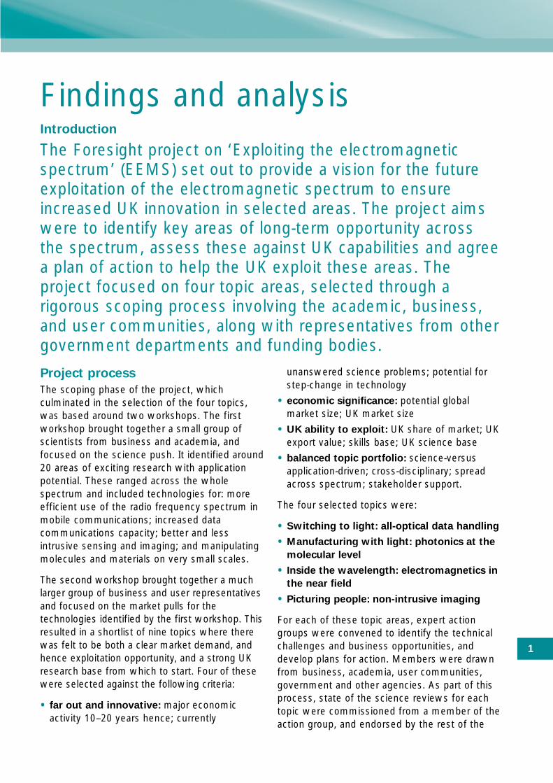
Switching to light: all-optical data handling
Summary
Over the last 20 years, optical fibre has becomethe dominant long-distance transmission mediumfor data communications, with copper wire (orradio) used mainly for the ‘last mile’ link to theuser. Although data is now transmitted optically,routing and switching continues to be carried outelectronically. For current and near-future data-traffic demands, this is both cost-effective andadequate. But if widespread demand reachesterabit levels (one terabit per second = 1012 bitsper second), existing and easily foreseeableelectronic technologies will have difficultykeeping up. Optical techniques will then need toform an increasingly large part of switching androuting systems in order to satisfy expectedfuture traffic levels. The UK could capture a
market of $0.5 billion in 10 years’ time in fast
optical switches, if it invested now in the
UK’s excellent science expertise in this area.
This is a high-risk venture, because of theuncertainty over whether fast optical switcheswill be needed by then, the likely globalcompetition and the risk that the UK will not
have a home market, which is perhaps essentialto compete successfully in the world market.
The key issue for the development of a homemarket is the provision and use of high-rate (100 Megabit/sec) broadband to the home/user. The decision to roll out high-rate broadband
for all rests on wider economic and social
considerations but, if taken now, would offer
the chance that the UK might also capture
the commercial opportunities.
Introduction
The cost and energy burden of converting
signals from optical to electronic and back
again when processing and routing becomes
ever greater as data networks become more
complex and data rates increase. Conversion
could be avoided if these functions were
carried out optically. The low cost and logic-friendly nature of silicon means that it is likely toremain unbeatable for certain functions but,above some data capacity threshold, furtherincreases in capacity will only be deliveredthrough increased use of optical components innew hybrid optical/electronic systems.
These hybrid systems will provide complexnetworks with the flexibility and performance toevolve to meet ongoing future requirements oflocal broadband systems and distributedcomputer processing. Promising hybrid systemsunder investigation keep the data signal in opticalform but attach a routing label that is processedelectronically. New network architectures thatreflect features of optical processing (such asburst processing of signal packets) will also be needed.
There are major science and engineeringchallenges to the commercial production ofoptical components. For example, a critical partof optical processing is an optical photonicmemory with a performance to match or exceed

6
that of the ubiquitous electronic RAM (randomaccess memory). At present there is no methodof storing and reading out data optically althougha variety of methods are under investigation.
Other techniques that could enable fast opticalswitching, including nonlinear optics and fasttuneable lasers, are also advancing rapidly.Photonic bandgap structures which cancompress light into very small spaces, makingdevices much more efficient (and potentiallylower cost), appear particularly promising.
Key drivers
For there to be a market for fast optical
switches, the action group agreed that
demand for data transmission rates would
need to reach terabit level in the network.
Such demand would be generated by a‘knowledge economy’ where value is placed onfast access to increasing amounts of globallyaccessible information. If the future is movingtowards a world of remote working – andplaying – in the widest sense of connecting in adata-rich way with experts or databases at adistance, the capability of existing technologiesto deliver the necessary information to the rightplace in an acceptable time will be put underincreasing strain.
New data is currently being generated at a rateof 2 exabytes (2 million terabytes) per year (250 megabytes for every person on earth).Companies rely ever more heavily oncomputerised records, and legal obligations tokeep data are growing. Increasing personal useof information technology is likely to lead to agrowth in demand for consumer data backupfacilities. Stored information is useless withoutrapid access for all who need it.
In addition to the corporate knowledge economy,there are other data-transmission-intensivemarkets, particularly ones such as video andtelepresence involving images, which might drivenetwork demand to terabit levels. These include:multimedia consumer gaming and video-on-demand; remote management of disasters byexperts; comprehensive security systems; andfully integrated electronic patient records.
It is difficult to estimate how fast demand isgrowing, and thus when it might reach terabitlevel, but most estimates are in line with therecent comments of Eric Mentzer, Intel’s Vice-President and Chief Technology Officer:
‘[Broadband and new multimedia
applications] are going to continue to
drive bandwidth on the optical
backbone… The net result of all this is
incredible growth in the Internet. What
is our network going to need to scale
to? It will be about a thousand times. If
it keeps up with this, which we think it
will, we'll need a network that can carry
a thousand times as much traffic ten
years from now.1’
Current capacity to broadband-equipped homesin the UK is ~1 Mb/sec (one megabit is 106 bits).A thousandfold increase takes this to 1 Gb/sec(one gigabit = 109 bits), which corresponds todata rates of hundreds of terabits in the networkbackbone. A more cautious estimate of 100 Mb/sec to the home in ten years would still imply the need for fast optical switching.
Although global markets for fast optical
switching technology could exist without
there being a UK home market, a home
market is probably essential if the UK is to
build an industry in this area. Growth indemand in the UK is presently hampered by alack of broadband capacity, and without access,demand cannot grow. This barrier is principallyeconomic: the cost of providing fibre to thehome to around 95% of the population isestimated at £10–20 billion. The current open-access-to-infrastructure regulatory framework inthe UK reduces the incentive for individualcompanies to invest in infrastructure. Whilstconsumers may be prepared to pay forinfrastructure if there are ‘must have’applications they desire, this is unlikely to createnetwork-wide demand fast, and is alsosomething of a chicken and egg situation. Aworkable business model to support investmentis needed. Japan is currently rolling out a 100 Mb/sec subscription service, but costs percapita would be much higher in the UK (due tolower population densities and underground
1 Eric Mentzer, Optical Fiber Conference 2003

7
Switching to light: all-optical data handling
Table 1. Market estimates for fast optical switches
Investment costs – three R&D phases plus one-off pre-production costs
installation of fibres – the Japanese are installingthem above ground).
The group’s assessment was that a public policyinitiative would probably be required to bringhigh-rate broadband to the home. This could takethe form of regulatory changes to allowbusinesses to keep control of their owninvestment in infrastructure, or to makeinstallation compulsory in new buildings. Whilst
wider social and economic considerations are
likely to be the primary motivation for a high-
rate broadband initiative, a clear and early
decision would allow the possibility that the
UK might also benefit commercially as well.
Markets and applications
Delivering terabit-level data rates will require fastoptical switching and routing systems. Ratherthan replacing existing electronics systems withall-optical ones, the new systems are likely to behybrid, with optics fulfilling the requirementsthat electronics will not be able to meet. Themain application areas identified for the use ofoptical technologies within the network were:
• storage area networks
• GRID equipment
• computer interconnects.
These would provide the network infrastructurefor high-capacity connections to storage, and fastretrieval and processing of data in distributeddatabases. Off-site data storing needs to be easy
for the user, fast and secure, and allow for largespikes in demand (such as end-of-the-day backingup). To be most efficient, the network needs tobe dynamic, user-defined/controlled and fullyintegrated. Rather than the route a signal takesbeing assigned by the network operator, the routewould be decided by the user. There are manyissues of data privacy, legal and industrystandards, copyright and protocols to be defined.Industry standards, which could have importantknock-on effects, are likely to be determined bythe main players. To have a say in establishingstandards the UK needs to be part of this newindustry. It is likely that new business models forselling services will evolve to reflect the featuresthat the customer regards as most valuable.
The action group’s ‘best guess’ estimate for thevalue of the global market for fast opticalswitches in 8–10 years’ time was $16 billion.They thought that the UK could capture a shareworth $0.5 billion (see Table 1). An investment ofaround $15 million is required for the initial 5-yearresearch phase, which would result in a packagedprototype switch with a demonstrated route toscaling the port count (with passive assembly).The milestones for the short second and thirdphases would be, respectively: developing arepeatable process for fab/packaging large portcount switches with initial reliability testing; andfully qualifying this process, adding electricalinterfaces, automated assembly and customersampling. The total time to market was estimatedat 8.5 years.
Phase 1 Phase 2 Phase 3 Pre- Total Value of World UK shareInitial (duration) (duration) production investment UK share marketinvestment (duration) cost (total of market(duration) duration)
Best guess $15 million $20 million $30 million $150 million $215 million $0.5 billion $16 billion 3%of UK (5 years) (1 year) (1 year) (1.5 years) (8.5 years)market size
Optimistic $32 billion $160 billion 20%market size(20% likelihood)

8
The group’s optimistic estimate (20% chance) ofthe value to the UK was $32 billion. The verylarge spread in value reflects the highly uncertainnature of this investment, which would involvesetting up new robotised production methodsand competing against the US and others whoare already investing heavily in the basictechnologies. The UK is, however, well placed interms of photonic and system expertise, andmany of the underlying technologies will havespin-off applications to provide revenue streamalong the way. The high degree of uncertainty,
together with the small initial investment
costs make this an attractive option since the
cost of ‘staying in the game’ is low compared
to the potential returns, and the major
investment costs are those of pre-production,
which may be deferred until later.
On a longer timescale (beyond 15 years), thegroup considered that niche applications takingadvantage of specific optical properties mightemerge outside the communications sector. Forexample, optical pattern recognition techniquesfor reading data labels could find wider use inpattern matching. In the even longer term, thegroup noted that storage, rather than access,may become the bottleneck, although solutionsto this are unlikely to be optical.
Technologies
At the heart of the anticipated optical
hybrid network would be fast (below
10 nanoseconds) optical switches, initially in
100 x 100 port count arrays. In these switches,light would act directly and efficiently on otheroptical signals, routing them without the needfor an electronic intermediary. To do so requiresvarious combinations of:
• wavelength-agile components, using cheaptuneable lasers so that signals can beswitched by changing their wavelength
• hybrid integrated, scaleable component arraysfor space switching
• optical buffer memory to store signals for bit-level switching, likely to involve using photonicbandgap structures in the future
• multi-wavelength optical regenerationcomponents to restore degraded signalstrengths
• scaleable Optical-Electronic-Optical (OEO)edge routers to handle the interface betweenoptical and electronic processing.
These components will need to be power-efficient, scaleable and low cost. Theirdevelopment will depend on more genericintegrated photonic platform technologies,dense integrated optics and materials with veryhigh nonlinearities. Cheap compact tuneableshort pulse lasers are also essential.
Other important issues include developingfuture-proofed (dynamically reconfigurable)network architectures to play to the strengths ofthe new switching technologies.
In addition to the unanswered basic researchquestions, there are significant new production-advancement requirements, including:
• high-yield reliability monitored fab/automatedproduction of switch arrays
• uncooled optoelectronic components, withthermal management of the arrays
• development of a cost-effective hybridintegration platform for photonics andelectronics
• protocols and standards (quality control).

9
Switching to light: all-optical data handling
NO
W5
ye
ars
10
ye
ars
15
ye
ars
TechnologiesApplicationsDrivers
OR
wir
eles
s/R
F
Dev
elo
pm
ent o
f exi
stin
g
(tel
eco
m) t
ech
no
log
ies:
Ho
me
ente
rtai
nm
ent
gam
ing
/vid
eo T
VG
row
th in
'kn
ow
led
ge
eco
no
my'
,co
mm
erci
al d
ata
sto
rag
e an
d a
cces
sD
isas
ter
man
agem
ent
Op
tica
l pat
tern
mat
chin
g
~10
p s
ecs
Wav
elen
gth
cir
cuit
switc
hes
Op
tical
bu
rst s
witc
hes
Low
-co
st O
EO
All-
op
tical
net
wo
rk
man
agem
ent
Mes
h c
on
nec
tivity
@ 2
0 T
b/s
ec/n
od
e20
0 n
od
es
Op
tical
net
wo
rks
(sec
on
d g
ener
atio
n)
Wav
elen
gth
co
nve
rsio
n
for
op
tical
cir
cuit
switc
hin
gO
ptic
al a
mp
lifie
rs
Inn
ova
tive
use
of
exis
ting
infr
astr
uct
ure
–c
able
/du
ct
Op
tical
net
wo
rks
(fir
st g
ener
atio
n)
Op
tical re
gen
era
tio
n
- M
ult
i w
avele
ng
th
- S
cale
ab
le
New
(n
on
-tele
co
m)
tech
no
log
ies f
or
>40 G
b/s
ec b
ackp
lan
e
Op
tical
bu
ffer
m
emo
ry
Ag
gre
gat
ion
(n
on
-tel
eco
m)
Wild
card
tech
no
log
ies
to r
edu
ce
cost
of f
ibre
to th
e h
om
e
3D o
ptic
al d
evis
es
Ag
ile c
om
po
nen
ts
Data
co
mp
ressio
n
New
app
licat
ion
s
Sec
uri
ty –
pri
vate
net
wo
rks?
Ch
eap
saf
e lo
w p
ow
er
Tele
pre
sen
ce
Fast
scale
ab
le
op
tical sw
itch
<10 n
an
osecs
Po
rt c
ou
nt
100 x
100
Need
to
sta
rt o
n f
ast
op
tical sw
itch
so
on
1 M
b/s
ec1
Gb
/sec
Gro
win
g r
esid
enti
al b
road
ban
d c
apac
ity
2.3
Gb
/sec
100
Gb
/sec
40 G
b/s
ec
Gro
win
g n
etw
ork
cap
acit
y
1 T
b/s
ec
Op
tical
qu
ality
of
serv
ice
mo
nito
rin
gLe
gac
y in
teg
ratio
n
Use
ph
oto
nic
b
and
gap
?
Ch
eap
tun
eab
le
lase
rsH
igh
ly n
on
linea
r m
ater
ials
Fib
res
to a
llh
om
es/o
ffic
es. C
ost
£10–
20 b
illio
n to
last
3 k
mO
EO
ed
ge
rou
ter
• S
cale
abili
ty t
o 2
00 T
b/s
ec•
100-
no
de
net
wo
rk (
or,
5,00
0 n
od
es (
as U
K
to
day
) +
4 T
b/s
ec r
ou
ters
)
WD
M•
Tun
eab
le s
ou
rces
• S
witc
hes
– M
EM
S
Free
-sp
ace
op
tics
Twis
ted
pai
r 2
Mb
/sec
(DS
L)C
o-a
x to
10
Mb
/sec
Fib
re to
the
curb
/bas
est
atio
n c
ost
<£1
0 b
illio
n
Au
tom
ated
as
sem
bly
etc
ST
OR
AG
E A
RE
A N
ET
WO
RK
SG
RID
NE
TW
OR
KIN
G
CO
MP
UT
ER
INT
ER
CO
NN
EC
TS
•1,0
00 p
roce
ssin
g n
od
es, 4
0 –
100x
ed
ge
den
sity
Key
net
wo
rk s
ervi
ces
Reg
ula
tory
issu
es,
pro
toco
ls, l
egal
an
d
net
wo
rk s
tan
dar
ds
Un
iver
sal s
ervi
ceE
qu
alit
y o
f ac
cess
Dat
a p
riva
cy
US
Do
E
fun
din
g p
rog
ram
me
Figure 1. All-optical data handling: technology timeline for fast optical switches (key steps shown in orange)

10
The way forward
If demand for network data transfer rates
were to reach terabit levels, it would exceed
the capabilities of existing switching and
routing technology. The UK is well placed to
develop fast optical switching technologies to
meet this need. The UK might capture a shareof the global market of between $0.5 billion and$32 billion. There are a number of issues to beconsidered:
• the uncertainty as to whether or when fastoptical switches will be needed
• the risk that the UK will not have a homemarket, which is perhaps essential to competesuccessfully in the world market
• the likely global competition.
The key steps to help the UK maintain its
lead in the science in this area and keep open
the option for further investment at a later
stage to capture a share of the market,
should the demand arise, are:
• a co-ordinated and visionary strategy by
the photonics community
• an initial investment of around $20 million in
R&D, to support existing UK centres of
research excellence in integrated photonics
technology. Research should be industry-led
to leverage this investment effectively
• a commitment to high-bandwidth
broadband rollout.
Since many of the underpinning technologies(for example, cheap tuneable lasers and cost-effective hybrid integration platforms) will haveextensive use in other applications and markets,activity should probably form part of a nationalphotonics roadmap providing a strategy forphotonics both in and outside of thecommunications sector (that is, combining withthe ‘Manufacturing with light: photonics at themolecular level’ topic recommendations).
This opportunity, among others, will be
considered by the DTI Electronics team’s
newly formed Photonics Strategy Group,
which will identify opportunities and
challenges for the UK over the next 5–10
years and develop an action plan to exploit
the sector. The team is also working to bring
together key players to start a national
Photonics network along the lines of the
successful Fuel Cells initiative.
Photonics has also been identified as a
potential priority area for a Call in 2004/05
under the new DTI Technology Strategy.
Acknowledgements
We would like to thank all members of theaction group who gave so generously of theirtime and expertise.
Ron Ballingall, DSTL
Dr Peter Batchelor, DTI
Professor Polina Bayvel, University College London
Dr Andy Carter, Bookham Technology plc
Dr Russell Davey, BT
Dr Michael Dueser, University College London
Steve Ferguson, Marconi
Dr Patrick Gill, National Physical Laboratory (NPL)
Professor Michael O’Mahoney, University ofEssex
Vince Osgood, EPSRC
Professor David Payne, Southampton University
Dr Alistair Poustie, Centre for IntegratedPhotonics
Ian Williams, DTI
State of the science review authors: ProfessorPolina Bayvel, Dr Michael Dueser and ProfessorJohn Midwinter, University College London.
11
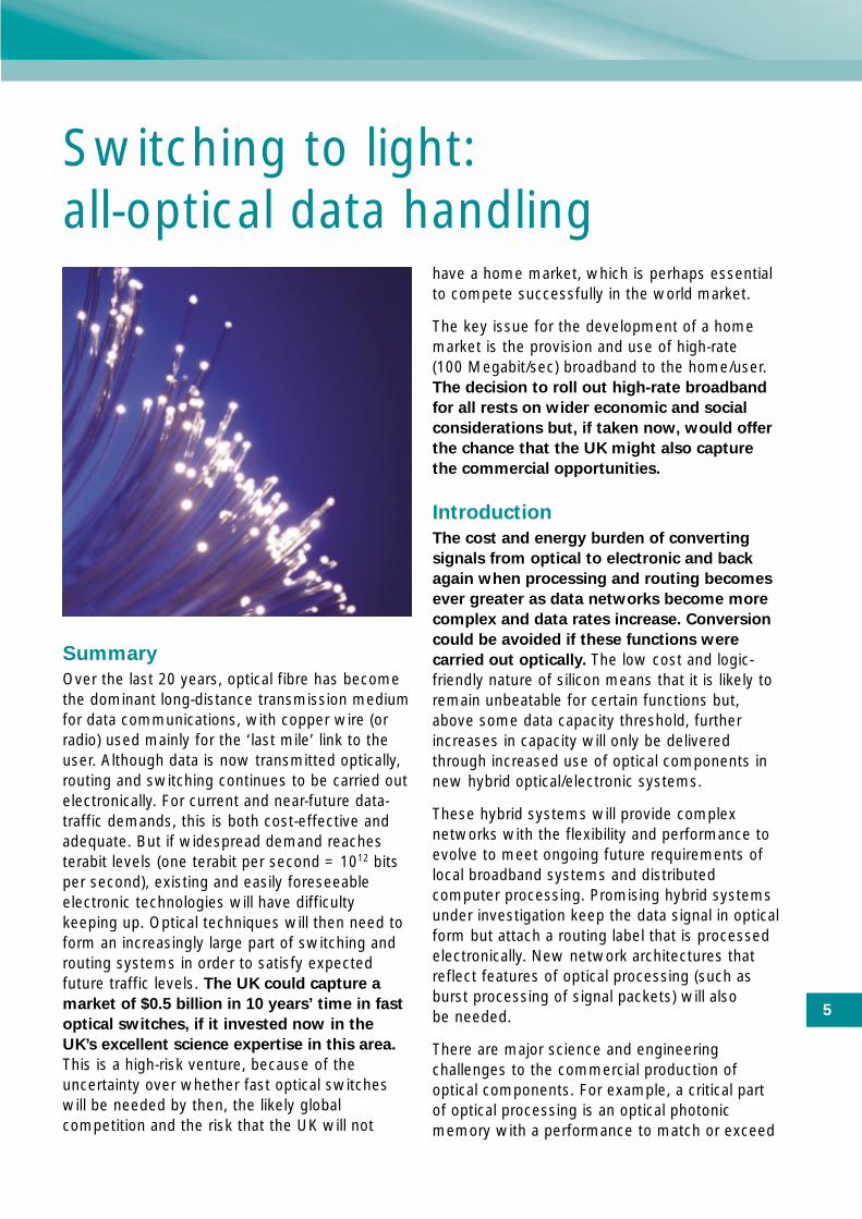
Manufacturing with light:photonics at the molecular level
Summary
Lasers have long been used for precisionmachining but as control becomes ever finer andfaster, light now offers the ability to manipulatematter on a molecular scale.
Laser micromachining in three dimensions
offers many manufacturing opportunities,such as the fabrication of microstructuredmaterials for next-generation solar cells, smartfibres, photonic crystals and photonic lab-on-a-chip devices.
The UK could capture a $5 billion market in
integrated lab-on-a-chip systems, as a
platform technology for a number of
multi-diagnostic applications, including
diabetes treatment, health monitoring,
drug targeting and cancer detection. In thelonger term, this could lead to therapeuticapplications, though these require an order ofmagnitude more investment in regulatory trials.Extrapolating the historical market growth rateand current size, this lab-on-a-chip market couldbe $100 billion by 2012. Capturing a niche of
even 5% of this is a significant opportunity thatthe UK is in a strong research position toaddress. These applications tend to have high
capital costs of setting up production, but
the potentially huge markets mean that the
relatively low initial research investment
costs are an attractive, if risky, proposition.
Introduction
More and more new developments in
microelectronics, integration and micro- and
nano-technologies require three-dimensional
structures, often made from materials that
are difficult to work with. Laser machining isadaptable to a wide range of materials and issurprisingly gentle (able to cut soft and biological materials without damage) so will play an important part in the production of these microstructures.
Large-scale precision machining did not formpart of the scope of this topic, and the actiongroup identified two broad areas for the focus oftheir work.
Micro and nano fabrication techniques nowbeing demonstrated in research laboratoriescould, if commercialised, produce the kinds ofmultiple-material microstructures needed for awide range of applications including next-generation solar cells, smart fabric, intelligentfibres (sensors) and photonic crystals. Aparticularly promising application is thefabrication of an advanced lab-on-a-chip (LoC).
Integrated photonic LoC will, in addition tobeing fabricated using photonic and lasertechnologies, also rely on them for its functionalcapabilities. Current LoC devices are mainlypassive microarrays of up to tens of thousandsof test sites at which are located specificmolecules or chemicals that test for a particularfunction. DNA chips, in which the testmolecules identify particular genetic sequences,

12
are the most common, but protein arrays arealso an important market.
An integrated photonic LoC would actively sortmolecules or particles using arrays of lasers(‘optical tweezers’) to push different moleculesin different directions as they flow through the‘optical lattice’ created by the laser beams.Preliminary experiments have shownpossibilities here and exciting newdevelopments in lasers and photonics offer theprospect of integrating many other specificfunctions on a single chip to offer multi-diagnostic capability in the future.
Key drivers
The market drivers for specific applications oflaser/photonic micromachining are diverse. Withincreasing pressure on global energy resources,improved energy efficiency (particularly, thoughnot exclusively, for portable devices) is set tobecome an ever more important considerationacross the board. Cost reduction andminiaturisation/portability are common drivers inmanufacturing, which are bolstered by trendstowards increasing personalisation of servicedelivery. They can also drive the opening up ofnew markets and ‘throw-away’ applications.Demand for environmental monitoring is rising:comprehensive surveillance of pollution ornatural resources requires small cheap low-maintenance sensors.
The overarching long-term driver for LoC
applications is healthcare and the rising
expectations of ageing but affluent societies
prepared to pay for the best available care.
Fast, efficient multi-diagnostic tests are an
essential part of evidence-based diagnostics.
They improve prevention, detection andtreatment of disease, and the matching oftreatments to the specific needs of individualpatients.
In recent years, it has become increasingly clearthat genetics affects not only predisposition todisease but also the efficacy of currentgeneration drugs. As Dr Allen Roses ofGlaxoSmithKline recently acknowledged, asmany as 90% of prescription drugs work in only
30–50% of the population. Despite thesignificant ethical issues surrounding genetictesting, the benefits in terms of preventativeand prescriptive treatments are likely to prevailand lead in the long term to the individualtailoring of drugs. This science ofpharmacogenomics offers the prospect of farbetter-targeted and efficient prescribing,screening patients both for the most appropriatedrug and for those likely to cause them adversereaction. Greater prescribing efficiency alsopromises large potential savings on drugspending, although whether this would lead toany reduction in overall spend is unclear (thesavings may simply be used to make moreexpensive drugs available to more people). Indue course this could lead to highly personalised‘chip therapy’, but because of the considerableregulatory hurdles faced by new therapeutics,the action group felt that over the next 10–20years the driver for LoC in healthcare would bediagnostic rather than therapeutic.
In the shorter term, and covering the periodwhere any new healthcare diagnostic would berequired to undergo trials, photonic LoCtechnology offers the prospect of meetingdemand for more efficient development of newpharmaceutical drugs (where the discovery cyclecurrently takes 10–15 years). It is also likely toprovide better research tools across a range ofbiosciences, including exciting areas of researchsuch as genomics and proteomics.
The growing demands for many types ofenvironmental monitoring – pollution, foodtoxins, chemical hazards – may provide a marketfor chemical use of LoC technology. There are,however, many competing technologies in thesesectors, so chemical uses are unlikely to be themain drivers for development (at present,virtually all uses of LoC are biological, so muchso that the term ‘biochip’ is used almostsynonymously).
Markets and applications
Micro and nano fabrication
Micro and nano scale fabrication methods willhave a wide range of applications. The action

13
Manufacturing with light: photonics at the molecular level
group considered in detail the market for three-
dimensional microstructured materials fornext-generation solar cells, low-intelligencemicrofibres for distributed sensing (of theenvironment, fire, biohazards), fabrics and paintsfor camouflage. The photovoltaic solar cellmarket is currently dominated by Japan, whoaccount for 70% of the manufacturing capacityin a market with significant overcapacity atpresent, although this is likely to change as useof fossil fuels becomes more expensive.
The group estimated that the UK might
capture 20% ($2 billion) of a market worth
$10 billion in 12 years’ time, for a total
investment of $580 million. They estimatedthat there was a 20% chance of the marketbeing $30 billion and the UK capturing 25% of it.The goals of the three phases of research weredefined as: (1) a scaleable manufacturingtechnology for making smart fabric and solarcells from a single material; (2) the same outputbut made from a number of materials bondedtogether (junctions between different materialsis a particular issue); (3) development ofpackaging, integration and prototyping. Thephased stages of the investment costs makethis a reasonably appealing proposal.
The group also considered the smaller marketfor the fabrication of application-specific
polymers produced in a minifab foundry, andthe litho tooling market – making themanufacturing tools rather than the end, userdevices. At present the principal known
application for these tools is display screenmanufacture. The key research phases hereinvolve developing reconfigurable masks usingspatial light modulators, and developing newresist materials in three dimensions, to achieveetching of giga-pixel resolution, but the highinvestment costs make this less suitable for UK exploitation.
Integrated photonic LoC
The short-term market for photonic LoC will bein research and development laboratories,enabling high-throughput precision-controlledsynthesis of chemicals and biochemicals forbiological purposes, and sorting and selection ofparticles and molecules. This market is a high-end, high-cost, low-volume one, in contrast tothe slightly longer-term healthcare diagnosticmarket, where the cost of a test will need to becomparable with the cost of a prescription. Key
target applications for diagnosis include
diabetes, drug targeting, cancer detection
and health monitoring (both of potentially
threatening conditions such as heart
problems and of ‘wellness’ functioning in
performance sports). Early applications wouldbe single diagnosis, with multi-diagnosticfunctionality and improvements in devicemobility following at a later stage.
The action group drew on the data supplied byFreshMinds and their own knowledge of thecurrent prescription market (there are currently10 billion prescriptions annually worldwide at acost of $1–50) to estimate the size of the
Table 2. Market estimates for three-dimensional microstructured materials
Investment costs – three R&D phases plus one-off pre-production costs
Phase 1 Phase 2 Phase 3 Pre- Total Value of World UK shareInitial (duration) (duration) production investment UK share marketinvestment (duration) cost (total of market(duration) duration)
Best guess $100 million $80 million $200 million $200 million $580 million $2 billion $10 billion 20%of UK (4 years) (3 years) (3 years) (2 years) (12 years)market size
Optimistic $7.5 billion $30 billion 25%market size(20% likelihood)
14
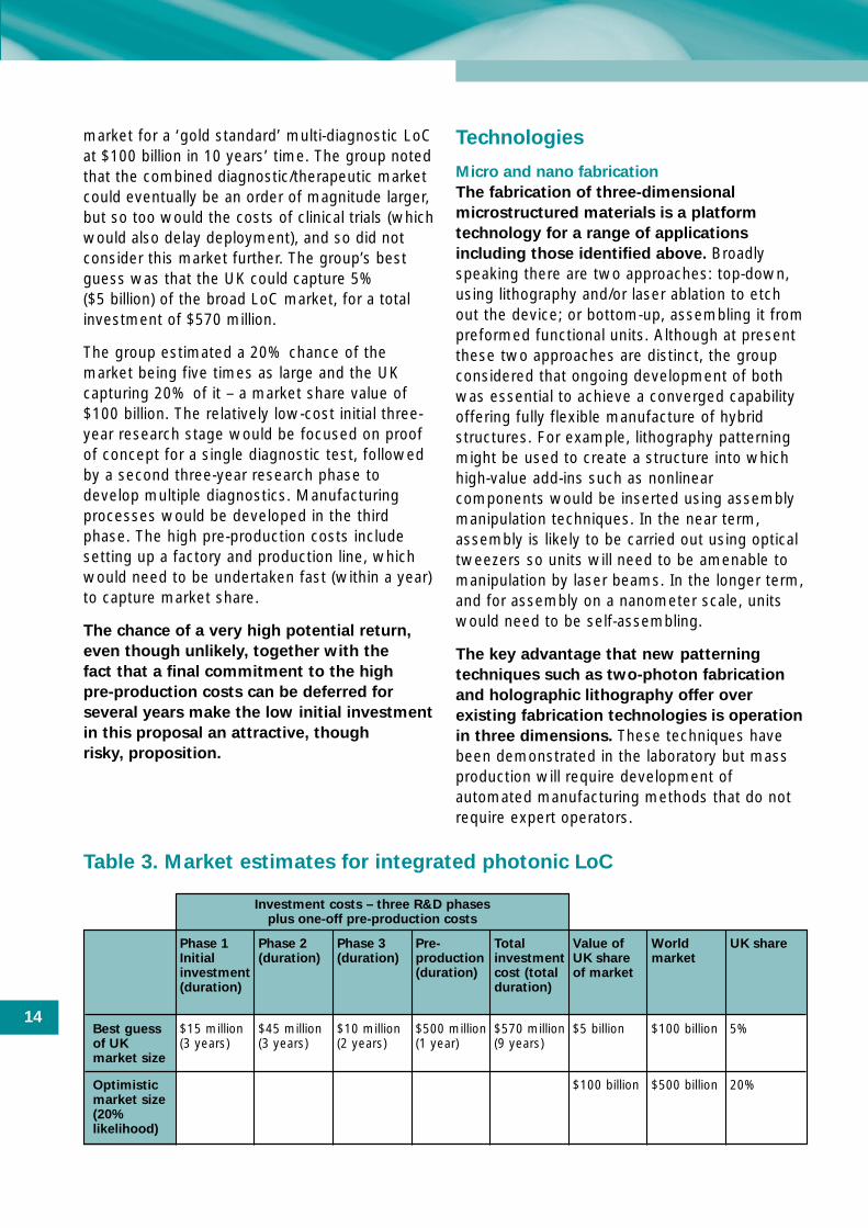
Table 3. Market estimates for integrated photonic LoC
Investment costs – three R&D phases plus one-off pre-production costs
Phase 1 Phase 2 Phase 3 Pre- Total Value of World UK shareInitial (duration) (duration) production investment UK share marketinvestment (duration) cost (total of market(duration) duration)
Best guess $15 million $45 million $10 million $500 million $570 million $5 billion $100 billion 5%of UK (3 years) (3 years) (2 years) (1 year) (9 years)market size
Optimistic $100 billion $500 billion 20%market size(20% likelihood)
market for a ‘gold standard’ multi-diagnostic LoCat $100 billion in 10 years’ time. The group notedthat the combined diagnostic/therapeutic marketcould eventually be an order of magnitude larger,but so too would the costs of clinical trials (whichwould also delay deployment), and so did notconsider this market further. The group’s bestguess was that the UK could capture 5% ($5 billion) of the broad LoC market, for a totalinvestment of $570 million.
The group estimated a 20% chance of themarket being five times as large and the UKcapturing 20% of it – a market share value of$100 billion. The relatively low-cost initial three-year research stage would be focused on proofof concept for a single diagnostic test, followedby a second three-year research phase todevelop multiple diagnostics. Manufacturingprocesses would be developed in the thirdphase. The high pre-production costs includesetting up a factory and production line, whichwould need to be undertaken fast (within a year)to capture market share.
The chance of a very high potential return,
even though unlikely, together with the
fact that a final commitment to the high
pre-production costs can be deferred for
several years make the low initial investment
in this proposal an attractive, though
risky, proposition.
Technologies
Micro and nano fabrication
The fabrication of three-dimensional
microstructured materials is a platform
technology for a range of applications
including those identified above. Broadlyspeaking there are two approaches: top-down,using lithography and/or laser ablation to etchout the device; or bottom-up, assembling it frompreformed functional units. Although at presentthese two approaches are distinct, the groupconsidered that ongoing development of bothwas essential to achieve a converged capabilityoffering fully flexible manufacture of hybridstructures. For example, lithography patterningmight be used to create a structure into whichhigh-value add-ins such as nonlinearcomponents would be inserted using assemblymanipulation techniques. In the near term,assembly is likely to be carried out using opticaltweezers so units will need to be amenable tomanipulation by laser beams. In the longer term,and for assembly on a nanometer scale, unitswould need to be self-assembling.
The key advantage that new patterning
techniques such as two-photon fabrication
and holographic lithography offer over
existing fabrication technologies is operation
in three dimensions. These techniques havebeen demonstrated in the laboratory but massproduction will require development ofautomated manufacturing methods that do notrequire expert operators.

15
Manufacturing with light: photonics at the molecular level
NO
W5
ye
ars
10
ye
ars
15
ye
ars
TechnologiesApplications
Mic
ro s
yste
ms
(op
tica
l, el
ectr
on
ic,
mic
rofl
uid
ic):
h
ybri
d s
yste
m o
n c
hip
Inte
gra
ted
o
pti
cal
circ
uit
Op
tica
l sw
itch
b
ased
on
3D
ph
oto
nic
cr
ysta
l
Low
-co
st, s
imp
le
to u
se, d
eep
U
V la
ser
sou
rces
; co
ntr
ol
Pre
fab
ricati
on
of
fun
cti
on
al b
locks
– s
elf
-assem
bly
?
Gu
ided
ass
emb
ly o
f (p
oss
ibly
sel
f-as
sem
ble
d) s
ub
un
its
Patt
ern
ab
le f
un
cti
on
al
mate
rials
Co
ntr
ol an
d
inte
gra
tio
n o
f syste
m
su
bfu
ncti
on
s f
or
hig
h v
olu
me, lo
w c
ost
Low
-in
telli
gen
ce,
low
-co
st:
• in
telli
gen
t fi
bre
s•
inte
llig
ent
pai
nts
Op
tica
l dir
ectl
y w
ritt
enm
icro
elec
tro
nic
s(p
rog
ram
mab
le)
Sta
rt
dev
elo
pm
ent
On
go
ing
dev
elo
pm
ent
FAR
FU
TU
RE
Lab
-on
-a-c
hip
:•
com
ple
x •
incl
ud
ing
val
ves
etc
• m
ult
iple
-mat
eria
ls
• 3D
arc
hit
ectu
re
All
3D in
la
bs
no
w
Pu
blic
per
cep
tio
n
of
nan
ote
ch
Op
tica
l or
chem
ical
?
Pro
cess
mo
nit
ori
ng
an
d c
on
tro
l
Sta
nd
ard
s
Hig
h-e
ffic
ien
cy
sola
r ce
lls
Inco
rpo
rati
on
of
fun
cti
on
al/
pre
fab
co
mp
on
en
ts in
to
3D
fra
mew
ork
Mic
ron
lith
og
rap
hy:
• d
eep
UV
• ~
200
nm
sca
le
• si
lico
n
Two
ph
oto
n
mic
ro fa
bri
catio
n
Rap
id
pro
toty
pin
gH
olo
gra
ph
ic
lith
og
rap
hy
New
fu
nct
ion
al
mat
eria
ls
Pat
tern
able
m
ater
ials
Two
-ph
oto
n
par
elle
lise
Mo
lecu
lar
reco
gn
itio
n
~nm
sca
le
Red
uce
co
st –
elim
inat
e n
eed
fo
r P
hD
to
op
erat
e
Mo
vin
g f
rom
vi
sib
le t
o n
ear
UV
sc
ale
(~10
0 n
m t
o 1
nm
)
Sca
le u
p t
o
larg
e vo
lum
es
at lo
w c
ost
Op
tica
l co
ntr
ol o
f ad
hes
ion
an
d
linka
ges
Par
alle
lism
of
twee
zers
– a
rray
la
sers
fo
r sp
eed
Fib
re r
esp
on
ds
to e
nvi
ron
men
t,
can
act
as
a se
nso
r o
r ac
tiva
tor
All
blo
cks
nee
d
to b
e 't
wee
zer
co
mp
atib
le'
Lase
r ab
latio
n:
• m
etal
s •
pla
stic
s•
cera
mic
s •
1 m
icro
n s
cale
Des
ign
of
fun
ctio
nal
b
lock
s an
do
vera
ll sy
stem
ar
chite
ctu
re
Man
ufa
ctu
rin
g
too
l d
evel
op
men
t
Mu
ltib
eam
para
llelise
Figure 2. Photonics at the molecular level: technology timeline for micro and nano fabrication(key steps shown in orange)
16
Critical issues include:
• multibeam parellisation – to deliver high-throughput speed in both patterning andassembly
• integration of functional prefabricatedcomponents into a three-dimensional structure
• patternable materials development: inparticular addressing the problem of junctionsbetween different types of base materials forstructures made of multiple materials
• high-volume, low-cost manufacturing controland integration processes.
Integrated photonic LoC
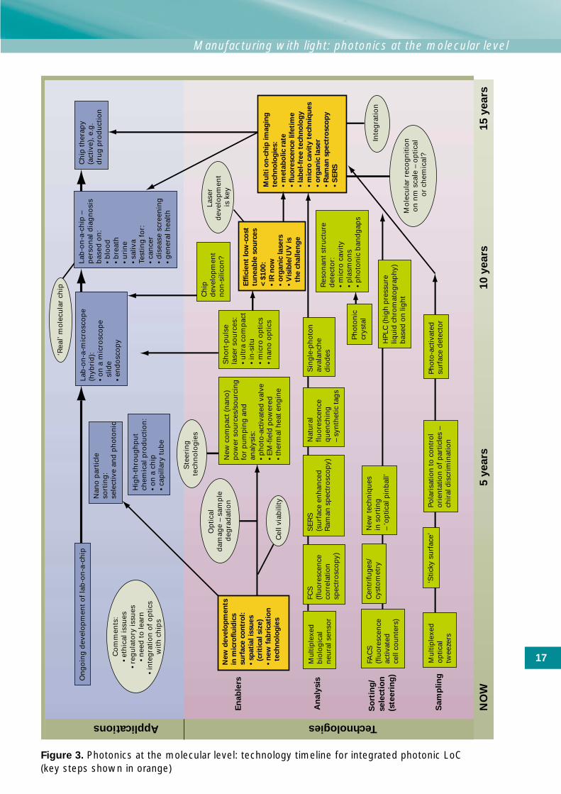
At present manipulation and selection in LoCsrelies on a limited range of physical andelectromigration effects (although the data outputis often optical). In the proposed photonic LoC thelight is used for new, more specific, diagnostics atsingle-molecule level, and for sensitive nonlineartechniques (requiring confinement of the light andvery short pulses). Light is also used for directselective manipulation using optical tweezer field-gradient effects.
Key elements of any LoC device are:
• sampling
• sorting/selection
• analysis
• ‘enabling’ functionality.
There are a number of alternative techniquesthat might deliver the first three of these. Manyinvolve near field effects, so there is someoverlap here with the ‘Inside the wavelength:electromagnetics in the near field’ topic. Adevelopment path may only need one of eachrather than all the options shown on thetechnology timeline. The critical technologies
are some of the ‘enabling’ ones:
• microfluidics: surface control, fabrication,
and spatial resolution
• laser sources: low-cost tuneable
lasers especially at visible and
ultraviolet frequencies
• detection: on-chip imaging, probably
integrating a number of modalities.
Integration of fluidics and optics into hybridchips is crucial, as is materials development. Tobe of use, test results will need interpreting:research will be needed to build up a databankof responses to enable this to be automated,especially in widespread low-end applicationssuch as health testing. The action groupenvisaged the degree of subjectiveinterpretation required falling off quite steeplywith time, with ease of use growing moreslowly (and costs falling). As with all data-intensive applications, software development forboth analysis and user interfaces is important.
Key technologies for both micro and nano
fabrication and integrated photonic LoC are
cheap compact lasers with total beam
control (shaping, pulses, tuning).
The way forward
The UK could reap rich rewards in the two
broad areas of:
• laser micromachining, driven by demands
for ever-smaller and cheaper devices
• integrated photonic lab-on-a-chip (LoC),
driven by demands for cheap multi-
diagnostics particularly but not solely
in healthcare.
The combined potential rewards for the UK fromthese areas could be around $7 billion. Themarket size for the integrated photonic LoC isvery uncertain, but offers a small chance of veryhigh returns. To seize these opportunities, anambitious visionary target is needed; withmarkets being so young we should not be overlyconstrained by the current industry position.
The UK has a strong science base in this area
and for a relatively small initial investment
could maintain this position and keep its
options open with respect to these markets,
both of which would require more substantial
investment at the later stages of R&D and
pre-production.
In addition to the two areas identified above,there is a wide range of potential uses of theunderpinning technologies in other applications.There are many basic science questions to
17
Manufacturing with light: photonics at the molecular level
NO
W5
ye
ars
10
ye
ars
15
ye
ars
TechnologiesApplications
On
go
ing
dev
elo
pm
ent
of
lab
-on
-a-c
hip
Ch
ip t
her
apy
(act
ive)
, e.g
.d
rug
pro
du
ctio
n
Ch
ip
dev
elo
pm
ent
no
n-s
ilico
n?
Lab
-on
-a-m
icro
sco
pe
(hyb
rid
):•
on
a m
icro
sco
pe
slid
e•
end
osc
op
y
Lab
-on
-a-c
hip
–
per
son
al d
iag
no
sis
bas
ed o
n:
• b
loo
d
• b
reat
h
• u
rin
e •
saliv
aTe
stin
g f
or:
• ca
nce
r•
dis
ease
scr
een
ing
• g
ener
al h
ealt
h
Nan
o p
arti
cle
sort
ing
:
sele
ctiv
e an
d p
ho
ton
ic
Hig
h-t
hro
ug
hp
ut
chem
ical
pro
du
ctio
n:
• o
n a
ch
ip•
cap
illar
y tu
be
Ste
erin
g
tech
no
log
ies
Lase
r d
evel
op
men
t is
key
Inte
gra
tio
n
Mu
lti o
n-c
hip
im
ag
ing
tech
no
log
ies:
• m
eta
bo
lic r
ate
• fl
uo
rescen
ce lif
eti
me
• la
bel-
free t
ech
no
log
y
• m
icro
cavit
y t
ech
niq
ues
• o
rgan
ic laser
• R
am
an
sp
ectr
osco
py
• S
ER
S
New
develo
pm
en
ts
in m
icro
flu
idic
s
su
rface c
on
tro
l:
• sp
ati
al is
su
es
(c
riti
cal siz
e)
• n
ew
fab
ricati
on
te
ch
no
log
ies
Ph
oto
nic
crys
tal
HP
LC (h
igh
pre
ssu
re
liqu
id c
hro
mat
og
rap
hy)
b
ased
on
lig
ht
New
co
mp
act (
nan
o)
po
wer
so
urc
es/s
ou
rcin
g
for
pu
mp
ing
an
d
anal
ysis
: •
ph
oto
-act
ivat
ed v
alve
• E
M-f
ield
po
wer
ed•
ther
mal
hea
t en
gin
e
Sh
ort
-pu
lse
lase
r so
urc
es:
• u
ltra
co
mp
act
• in
-sit
u
• m
icro
op
tics
•
nan
o o
pti
cs
Res
on
ant
stru
ctu
re
det
ecto
r:
• m
icro
cav
ity
• p
lasm
on
s •
ph
oto
nic
ban
dg
aps
Co
mm
ents
:•
eth
ical
issu
es•
reg
ula
tory
issu
es•
nee
d t
o le
arn
• in
teg
rati
on
of
op
tics
w
ith
ch
ips
Op
tica
l d
amag
e –
sam
ple
d
egra
dat
ion
Mo
lecu
lar
reco
gn
itio
n
on
nm
sca
le –
op
tica
l o
r ch
emic
al?
Cel
l via
bili
ty
‘Rea
l’ m
ole
cula
r ch
ip
En
ab
lers
An
aly
sis
So
rtin
g/
sele
cti
on
(ste
eri
ng
)
Sam
plin
g
Mu
ltip
lexe
d
bio
log
ical
n
eura
l sen
sor
FCS
(f
luo
resc
ence
co
rrel
atio
nsp
ectr
osc
op
y)
SE
RS
(s
urf
ace
enh
ance
dR
aman
sp
ectr
osc
op
y)
Nat
ura
lflu
ore
scen
ce
qu
ench
ing
–
syn
thet
ic ta
gs
Sin
gle
-ph
oto
n
aval
anch
e d
iod
es
FAC
S(f
luo
resc
ence
ac
tivat
ed
cell
cou
nte
rs)
Cen
trifu
ges
/cy
sto
met
ryN
ew te
chn
iqu
es
in s
ort
ing
–
‘op
tical
pin
bal
l’
Mu
ltip
lexe
d
op
tical
tw
eeze
rs
Po
lari
satio
n to
co
ntr
ol
ori
enta
tion
of p
artic
les
– ch
iral
dis
crim
inat
ion
‘Stic
ky s
urf
ace’
Ph
oto
-act
ivat
ed
surf
ace
det
ecto
r
Eff
icie
nt
low
-co
st
tun
eab
le s
ou
rces
< $
100:
• IR
no
w
• o
rgan
ic lasers
• V
isib
le/U
V is
th
e c
hallen
ge
Figure 3. Photonics at the molecular level: technology timeline for integrated photonic LoC(key steps shown in orange)

18
answer as well as the manufacturing challenges.It is important to co-ordinate a multidisciplinaryeffort: for the LoC, close involvement ofbiological and medical scientists is essential. Allthese factors indicate that support should formpart of a national photonics road map, building astrategy for photonics across all areas (that is,combining with the ‘Switching to light: all-opticaldata handling’ topic recommendations).
This opportunity, among others, will be
considered by the DTI Electronics team’s
newly formed Photonics Strategy Group,
which will identify opportunities and
challenges for the UK over the next 5–10
years and develop an action plan to exploit
the sector. The team is also working to bring
together key players to start a national
Photonics network along the lines of the
successful Fuel Cells initiative.
Photonics has also been identified as a
potential priority area for a Call in 2004/05
under the new Technology Strategy.
Acknowledgements
We would like to thank all members of theaction group who gave so generously of theirtime and expertise.
Professor Donal Bradley, Imperial College London
Nathan Davies, EPSRC
Professor Kishan Dholakia, St Andrews University
Michael Dunn, The Wellcome Trust
Professor Sir Richard Friend, Cambridge University
Dr Clive Hayter, EPSRC
David Hull, DSTL
Dr Andrew Kearsley, Oxford Lasers Ltd
Professor Thomas Krauss, St Andrews University
Dr Coulton Legge, GlaxoSmithKline
Dr Tom McLean, Avecia
David Robbins, Centre of Excellence forNanotechnology, Micro and Photonic Systems
Dr Shiv Sharma, Amersham plc
Professor Wilson Sibbett, St Andrews University
Professor Andrew Turberfield, Oxford University
State of the science review authors: ProfessorKishan Dholakia and Dr David McGloin, StAndrews University.

19
Inside the wavelength:electromagnetics in the near field
Summary
All Foresight projects seek to explore andestablish best practice for science futures work.To this end, we sought a balance betweentopics defined by application or market andthose defined by the underlying science. Thistopic is of the latter type and consequently itsapplication areas are more diverse. The nearfield is the confined non-propagating part of anelectromagnetic field (at any frequency) thatdecays away exponentially from a surface,within a distance of about a wavelength. Therecent UK-led discovery of ‘metamaterials’(composite artificial materials) will allowmanipulation and use of the near field in waysnot previously possible.
Near field technologies are critical to
developing smart antennas and integrated
radio frequency infrastructure and circuitry.
The UK has a strong industry presence in this
sector and there is already much short-termincremental development. Long-term goalsinclude wearable antennas, very accurate beamcontrol, integrated broadband antennas and lowSAR (specific absorption rate) antennas.
Metamaterials are opening up excitingpossibilities in other areas, such as sub-wavelength resolution imaging using‘superlenses’ especially in MRI (magneticresonance imaging). As yet there are no
obvious single applications that alone would
be of sufficient potential to justify focused
investment. More basic research is needed to
explore the full potential of metamaterials.
Introduction
In general, at whatever frequency in thespectrum, it is the propagating wave part of theelectromagnetic field that is exploited – whetherthat be radio waves transmitting information,visible light providing illumination or laser beamscutting materials. The full electromagnetic field,however, comprises both these travelling wavesand a non-propagating component that decaysaway very rapidly from emitting surfaces. Sinceit is negligible except within about a wavelengthof the surface, it is called the near field, althoughthe distance it extends over can be manymetres for low-frequency radio waves. Newly
discovered metamaterials offer prospects for
manipulation of the near field across a wide
range of frequencies and many diverse
applications.
Controlling the near field would enable many
advances in efficient radio communications:
reductions in interference, losses, energy
consumption and absorption of power by
human tissue. Over smaller distances, local

20
communications (for example, between smartdevices within the home) might be carriedentirely within the near field.
In addition to being highly localised and non-propagating, the near field can vary on scalesmuch smaller than the wavelength of theassociated propagating wave. If the near fieldcould be imaged, detail on sub-wavelengthscales could be resolved – detail that cannot beseen with propagating waves, whose resolutionis limited by their wavelength. Metamaterials area broad class of artificially created materials withelectromagnetic properties beyond any found innature. Some metamaterials have negativerefractive indices, which means that they bendlight in the opposite (negative) direction to thebending caused by all naturally occurringmaterials. This property opens up the possibilityof imaging the near field by creating a‘superlens’ with a negative refractive index to capture and image the information in the near field.
This could be of use in MRI where improvingresolution is currently achieved by increasing thestrength of the background magnetic field. Thisreduces the wavelength of the imaged signalbut high field magnets are expensive to makeand cumbersome to work with. As research intonegative index materials continues, there arelikely to be other potential applications for a superlens.
At metal surfaces and for frequencies in theoptical range the near field interacts with theconductance electrons in the metal to form a‘surface plasmon’. In metal foils patterned withholes, surface plasmons can cause radiation of amuch longer wavelength than the dimensions ofthe holes to be transmitted through them,something that at first glance seemscounterintuitive. Surface plasmons can containlocalised regions of very high field density,offering prospects that include: holding(bio)molecules in position for individual testing;on-chip communications; and powering nonlinearoptical effects (such as are needed inapplications like fast optical switches).
The action group considered three areas of
potential application of near field effects:antennas and electromagnetic interference
(EMI) control; MRI near field imaging; and
local near field communications and optical
bio-sensing.
Antennas and electromagneticinterference control
Key drivers
As described under ‘Switching to light: all-opticaldata handling’, global data transmissiondemands are growing and, whilst rates ofgrowth may fluctuate, the trend is likely tocontinue upwards. This is a key driver for bothfixed-line and mobile communications systems.Wireless traffic is growing and in the future maywell include increasing amounts of inter-devicecommunication between ever more intelligentdevices, such as smart home appliances, carnavigation systems and trackers for radiofrequency identity (RFID) tagged objects.Demand for more bandwidth will increase
pressure for more efficient use of the radio
frequency (RF) spectrum, for example,
through better beam control or by using
confined near field communications.
Consumer expectations create strong drivers forreducing the cost, size and weight of devices. Atpresent health concerns over SAR are not amajor driver – consumers show no preferencefor low-SAR models when buying phones – soproducers have little motivation to develop low-SAR devices. Were public opinion or regulationsto change, health concerns could rapidly becomeimportant. This possibility cannot be ruled out,especially as the network becomes morepervasive, and would be a major driver for verylow-SAR equipment.
Markets and applications
The antenna market is very cost-driven and theprice attrition that has seen unit costs formobile-handset antennas drop from $1 fouryears ago to $0.30 today is likely to continue.There is a wide range of product improvementsthat could be delivered if the market wasprepared to pay for them. The group considered
21
Inside the wavelength: electromagnetics in the near field
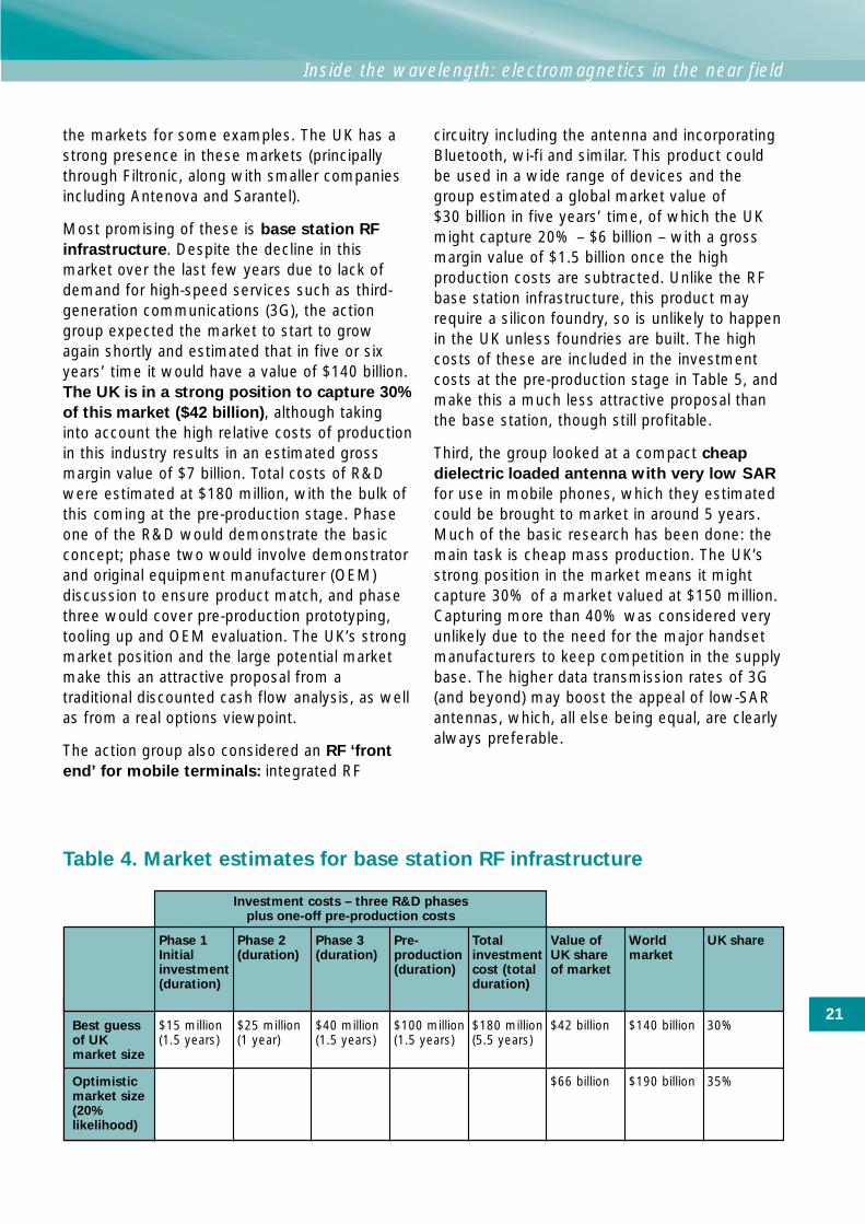
the markets for some examples. The UK has astrong presence in these markets (principallythrough Filtronic, along with smaller companiesincluding Antenova and Sarantel).
Most promising of these is base station RF
infrastructure. Despite the decline in thismarket over the last few years due to lack ofdemand for high-speed services such as third-generation communications (3G), the actiongroup expected the market to start to growagain shortly and estimated that in five or sixyears’ time it would have a value of $140 billion.The UK is in a strong position to capture 30%
of this market ($42 billion), although takinginto account the high relative costs of productionin this industry results in an estimated grossmargin value of $7 billion. Total costs of R&Dwere estimated at $180 million, with the bulk ofthis coming at the pre-production stage. Phaseone of the R&D would demonstrate the basicconcept; phase two would involve demonstratorand original equipment manufacturer (OEM)discussion to ensure product match, and phasethree would cover pre-production prototyping,tooling up and OEM evaluation. The UK’s strongmarket position and the large potential marketmake this an attractive proposal from atraditional discounted cash flow analysis, as wellas from a real options viewpoint.
The action group also considered an RF ‘front
end’ for mobile terminals: integrated RF
circuitry including the antenna and incorporatingBluetooth, wi-fi and similar. This product couldbe used in a wide range of devices and thegroup estimated a global market value of $30 billion in five years’ time, of which the UKmight capture 20% – $6 billion – with a grossmargin value of $1.5 billion once the highproduction costs are subtracted. Unlike the RFbase station infrastructure, this product mayrequire a silicon foundry, so is unlikely to happenin the UK unless foundries are built. The highcosts of these are included in the investmentcosts at the pre-production stage in Table 5, andmake this a much less attractive proposal thanthe base station, though still profitable.
Third, the group looked at a compact cheap
dielectric loaded antenna with very low SAR
for use in mobile phones, which they estimatedcould be brought to market in around 5 years.Much of the basic research has been done: themain task is cheap mass production. The UK’sstrong position in the market means it mightcapture 30% of a market valued at $150 million.Capturing more than 40% was considered veryunlikely due to the need for the major handsetmanufacturers to keep competition in the supplybase. The higher data transmission rates of 3G(and beyond) may boost the appeal of low-SARantennas, which, all else being equal, are clearlyalways preferable.
Table 4. Market estimates for base station RF infrastructure
Investment costs – three R&D phases plus one-off pre-production costs
Phase 1 Phase 2 Phase 3 Pre- Total Value of World UK shareInitial (duration) (duration) production investment UK share marketinvestment (duration) cost (total of market(duration) duration)
Best guess $15 million $25 million $40 million $100 million $180 million $42 billion $140 billion 30%of UK (1.5 years) (1 year) (1.5 years) (1.5 years) (5.5 years)market size
Optimistic $66 billion $190 billion 35%market size(20% likelihood)
22
Technologies
Much of the basic R&D has been achieved forshort-term products.
Key development areas include:
• low-loss materials – to reduce losses by halfto under 25%
• wide bandwidth (since there is a fundamentaltension between this and low losses, effectivewide band may need to be achieved byhopping between many narrow bands)
• high isolation – controlling cross-channelinterference both among classes of devicesand between different types of device
• integrated RF circuits
• adaptive materials
• flexible lightweight high-dielectrics
• low SAR (perhaps 20 times better thanpresent) through directional control of radiationbeams and lower power.
If SAR becomes a more serious issue, bettermodels of absorption by tissue and improvedSAR verification technology will be needed.
In the longer term, the group anticipatedantennas becoming small and lightweightenough to be wearable, for example, integratedinto clothing. Similar trends towards tiny lowpower base stations might open the way forsmart houses with pico-cell base stationsproviding a totally networked environment withno increase in radiation levels.
Magnetic resonance imaging (MRI)near field imaging
Key drivers
As explained more fully in ‘Picturing people: non-intrusive imaging’, increasing expectations forhealthcare are expected to be a major driver inexpanding medical markets in the future. Imaging
plays a key role in detection and treatment of
disease and there is strong demand for
improvements in functionality, safety,
efficiency, access and ease of use. MRI is one ofthe safest imaging modalities currently in use.Improving its resolution, and reducing the cost andsize of machines, would strengthen the relativeposition of MRI in the medical imaging market. Inthe long term, metamaterials may enable MRImachines to be sufficiently cheap and portablethat they could compete with ultrasound and x-rays in the ‘mass market’ of primary healthcare-centre imaging, rather than remaining the high-endspecialist modality they are at present.
Markets and applications
A particularly appealing feature of MRI as animaging modality is its safety: unlike x-rays,positron emission tomography (PET) or single-photon computerised tomography (SPECT), itdoes not involve ionising radiation. However, MRImachines have relatively poor resolution and arecostly and bulky. The last two are mainly due tothe magnets needed to produce the highmagnetic fields that create the conditions for
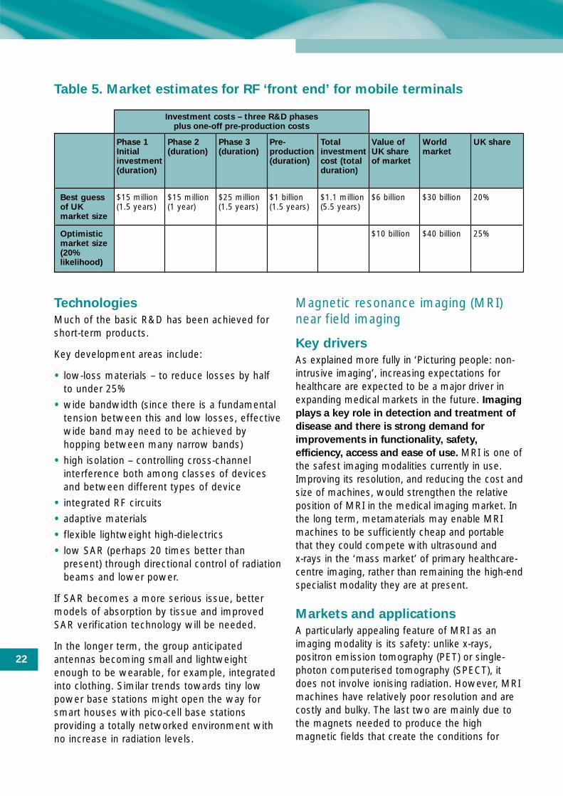
Table 5. Market estimates for RF ‘front end’ for mobile terminals
Investment costs – three R&D phases plus one-off pre-production costs
Phase 1 Phase 2 Phase 3 Pre- Total Value of World UK shareInitial (duration) (duration) production investment UK share marketinvestment (duration) cost (total of market(duration) duration)
Best guess $15 million $15 million $25 million $1 billion $1.1 million $6 billion $30 billion 20%of UK (1.5 years) (1 year) (1.5 years) (1.5 years) (5.5 years)market size
Optimistic $10 billion $40 billion 25%market size(20% likelihood)
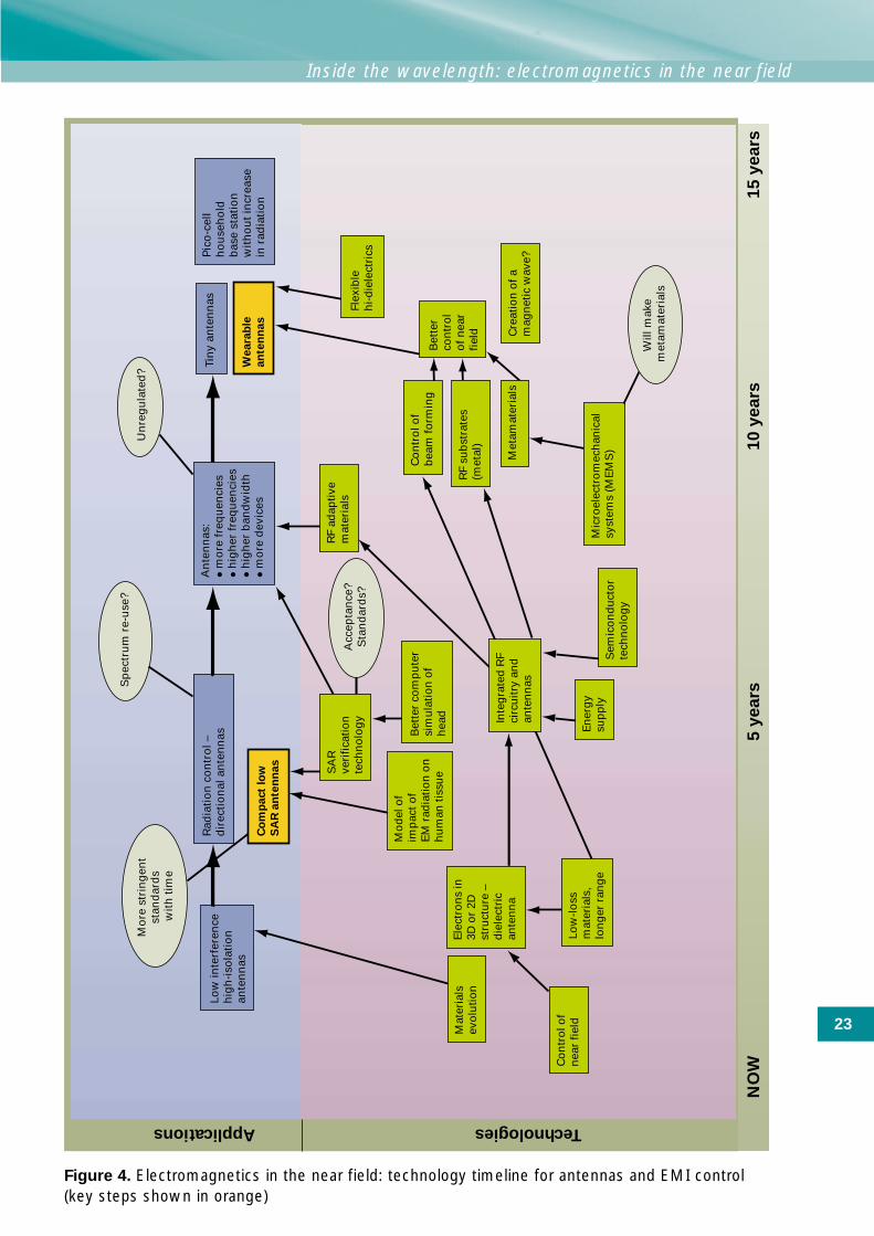
23
Inside the wavelength: electromagnetics in the near field
NO
W5
ye
ars
10
ye
ars
15
ye
ars
TechnologiesApplications
Pic
o-c
ell
ho
use
ho
ld
bas
e st
atio
n
wit
ho
ut
incr
ease
in
rad
iati
on
Inte
gra
ted
RF
circ
uitr
y an
d
ante
nn
as
Mic
roel
ectr
om
ech
anic
alsy
stem
s (M
EM
S)
Sp
ectr
um
re-
use
?
Rad
iati
on
co
ntr
ol –
d
irec
tio
nal
an
ten
nas
Tin
y an
ten
nas
Weara
ble
an
ten
nas
Low
inte
rfer
ence
hig
h-i
sola
tio
nan
ten
nas
Mat
eria
ls
evo
lutio
n
Low
-loss
m
ater
ials
,lo
ng
er r
ang
eE
ner
gy
sup
ply
Sem
ico
nd
uct
or
tech
no
log
y
Co
ntr
ol o
f n
ear
field
Co
ntr
ol o
f b
eam
form
ing
RF
adap
tive
mat
eria
ls
Met
amat
eria
lsC
reat
ion
of a
mag
net
ic w
ave?
RF
sub
stra
tes
(met
al)
Mo
del
of
imp
act o
f E
M r
adia
tion
on
h
um
an ti
ssu
e
Bet
ter
com
pu
ter
sim
ula
tion
of
hea
d
Flex
ible
h
i-die
lect
rics
Bet
ter
con
tro
l o
f nea
r fie
ld
Mo
re s
trin
gen
t st
and
ard
s w
ith
tim
e
Acc
epta
nce
?S
tan
dar
ds?
Un
reg
ula
ted
?
Ele
ctro
ns
in
3D o
r 2D
st
ruct
ure
–
die
lect
ric
ante
nn
a
SA
R
veri
ficat
ion
te
chn
olo
gy
Co
mp
act
low
SA
R a
nte
nn
as
Will
mak
e m
etam
ater
ials
An
ten
nas
:• m
ore
fre
qu
enci
es• h
igh
er f
req
uen
cies
• hig
her
ban
dw
idth
• mo
re d
evic
es
Figure 4. Electromagnetics in the near field: technology timeline for antennas and EMI control(key steps shown in orange)
24
resonance, and the associated screening neededto contain and isolate these fields. Resolution canbe improved by using higher field strengths,which requires even more expensive magnets.Specificity may be enhanced by the use of smartcontrast agents, as described more fully in the‘Picturing people: non-intrusive imaging’ topic.
Negative refractive index metamaterials offerthe prospect of improving MRI resolution byimaging the near field part of the radio frequencysignal, using a ‘superlens’, and of controlling theelectromagnetic fields so that they are targetedwhere wanted and screened from elsewhere.Machines could then be less bulky and wouldallow surgeons to perform in-situ operations. Inthe longer term, metamaterials developmentsmay facilitate portable MRI machines – maybeeven a stethoscope-style device.
The action group considered the market for anMRI multifunctional superlens. This productwould be an enhancement to future highresolution MRI machines (or possibly retrofittedto existing machines). The cost of theenhancement would be offset by reductions inhigh field magnet costs, and by gains in costefficiency: superlenses offer the possibility ofmuch faster parallel data acquisition, thusspeeding up the scanning throughput rate. TheUK has little presence in the MRI hardwaremarket, except in magnets, so the marketconsidered was just that for the superlens itself.This was estimated at $100 million, with the UKable to capture 20%. Consideration of the costsof development, in particular the establishmentof high-volume manufacturing processes for themetamaterials components, led to theconclusion that, despite the exciting science,there was not a clearly defined significantmarket opportunity for this particular application.
Developing a superlens remains an important
research challenge and, in the longer term,
metamaterials may provide the means to
produce portable MRI devices that could
command a much larger market than
enhancements to specialist high-end machines.
The group also considered the markets forreplacing the current copper screening ofdedicated MRI rooms with metamaterials. Their
evaluation indicated that the small screeningmarket value would not cover the costs ofdeveloping the necessary metamaterials, eventhough these would only need to screen thespecific frequencies used in MRI. Materialsproviding ‘broadband’ screening across a widerange of frequencies would have morewidespread applications, including militarystealth ones. The group concluded that, despitethe absence of a single large-market applicationfor metamaterials at present, there was a largenumber of niche applications based onessentially the same underlying technology, andthat more applications were likely to emerge asthe research field became more mature.
Technologies
A key technology challenge is manufacture
of the metamaterials components of
superlenses. Materials expertise from thoseinvolved in manufacture of similarly scaleddevices, such as capacitors, may be the route toa solution. Mass production would clearly beneeded for commercial production, butsignificantly more efficient methods are alsoneeded to facilitate further R&D into superlensapplications and into the general theory ofsuperlensing itself, which remains a topic ofmuch fundamental research interest.
In addition to the manufacturing challenge, thepotential applications in lenses and screening(such as, for example, a portable MRI‘stethoscope’) will require metamaterials thatare low-loss (a tenfold improvement over currentperformance), lightweight and flexible.
Local near field communications and optical bio-sensing
Key drivers
Depending on the radio frequency being used,local communications – over distances of up toseveral metres – cannot avoid being in the nearfield. In addition to offering a new channel ofcommunication, use of the near field also carriesthe advantage of being very localised, making iteasy, for example, to ensure that your smart fridgedoes not pick up your neighbour’s instructions.

25
Inside the wavelength: electromagnetics in the near field
NO
W5
ye
ars
10
ye
ars
15
ye
ars
TechnologiesApplications
Op
en m
agn
ets
enab
le
inte
rven
tio
nal
an
d o
rth
op
aed
ic
MR
I
Su
per
len
s to
pro
du
ce
no
n-p
lan
ar im
ages
, al
low
ing
co
mp
ensa
tion
fo
r n
on
linea
r m
agn
etic
fiel
ds
Su
perl
en
s t
o 1
mm
, o
r
even
0.1
mm
reso
luti
on
Scr
een
ing
of
low
-blo
od
fl
ow
are
as o
f b
od
y (e
.g. e
yes,
ure
thra
, b
rain
) fr
om
RF
fiel
d
(hea
tin
g e
ffec
ts)
Loca
tio
n o
f se
nso
rin
th
e b
od
y (r
adio
pill
) 1
cm r
eso
luti
on
Oth
er p
oss
ible
ap
plic
atio
ns
at lo
w s
pat
ial
reso
luti
on
(1
cm)
e.g
. MR
I sp
ectr
osc
op
y
Loca
l en
han
cem
ent
of
rad
iati
on
to
re
du
ce S
AR
; te
chn
olo
gy
avai
lab
le n
ow
Imag
ing
th
rou
gh
su
per
eso
luti
on
Bed
sid
e M
RI o
n
tro
lley
MR
I st
eth
osc
op
e?
MR
I 'te
nt'
–
scre
ened
roo
ms
Desig
n f
ine
str
uctu
re
meta
mate
rials
(fo
r 1 m
m r
eso
luti
on
)
Gra
nd
ch
allen
ge:
gen
era
l th
eo
ry a
nd
develo
pm
en
t o
f
su
perl
en
sLo
w-lo
ss
met
amat
eria
ls
– lo
ng
er r
ang
e
Cap
acito
r te
chn
olo
gy
1 cm
res
olu
tion
su
per
len
s (in
dev
elo
pm
ent n
ow
)
Scr
een
ing
ro
om
co
sts
£250
,000
at
pre
sen
t
Pat
ien
t co
uld
b
e sc
ann
ed t
hro
ug
h f
oca
l p
lan
e, w
hic
h is
tu
ned
to
mag
net
ic
reso
nan
ce p
lan
e
Co
ntr
ast
mec
han
ism
?(i
mp
rove
men
t o
f co
ntr
ast)
– k
ey
clin
ical
req
uir
emen
t
Co
st o
f n
ew
mag
net
sS
oft
war
e p
roce
ssin
g
of
dat
a
Use
silv
er r
ath
er
than
co
pp
er?
Aim
ing
fo
r 10
-fo
ld im
pro
vem
ent
‘Sw
iss
rolls
’ cu
rren
tly
1 cm
an
d
rig
id –
aim
to
red
uce
to
1 m
m
Co
sts
of
mat
eria
l >
£10,
000
Flex
ible
, th
in
con
stru
ctio
n
of m
etam
ater
ial
com
po
nen
ts
Man
ufa
ctu
re o
f fin
e-
stru
ctu
re lo
w-lo
ss
met
amat
eria
ls
Imp
rove
res
olu
tion
o
f sen
sor
det
ecto
rs
Mag
net
ic w
ires
an
d tr
ansm
issi
on
lin
es –
loca
l d
eliv
ery
of
RF
field
Op
en m
agn
ets
(with
res
olu
tion
fro
m
sup
er r
eso
lutio
n le
ns)
Figure 5. Electromagnetics in the near field: technology timeline for MRI near field imaging (key steps shown in orange)
26
The previous section on the ‘Manufacturing withlight: photonics at the molecular level’ topicdescribed drivers towards improved bio-molecular testing capabilities in greater detail.Demand for genetic testing – identification ofthe sequences of bases in DNA – is expected toincrease, for health treatment, for private orinsurance-related screening and inpharmaceutical drug development and testing.This will drive the development of fastertechniques, a demand that could be met by anumber of different technologies.
Markets and applications
As noted in the ‘Manufacturing with light:photonics at the molecular level’ topic, there area number of near field techniques that could beincorporated into an integrated photonic LoC forbio-sensing. The action group for the ‘Inside thewavelength: electromagnetics in the near field’topic considered the specific application of high-
throughput DNA molecular screening.Although there are competing technologies(including the polymerase chain-reaction methodswidely used today), the group felt that near fieldtechnologies might offer a promising solution inwhich the DNA base molecules to be testedwould be captured and localised by the near fieldon metal sheets patterned with tiny holes. Themolecules would then be identified usingscanning near field optical microscope (SNOM)probes, effectively performing single-moleculespectroscopy at each test site. There areconsiderable challenges to development, some ofwhich are not electromagnetic, including: devisinga way of streaming the DNA through the metalfoil; identifying accurate test reagents andestablishing the near field signal detectionprocess. The complexity of the technicalchallenges and the number of competingtechnologies make it difficult to estimate marketswith any degree of confidence.
The action group also considered local near field
communications over small distances such asthose covered by Bluetooth and wi-fi. This wouldbe an adaptive wireless personal grid, enablinginter-device communications between personalelectronic devices and also potentially your smartappliances at home. However, uncertainty over
competing technologies in this market led to theconclusion that it was difficult to assess thescale of this opportunity at present.
Probably beyond the timescale of this project,and too far for the group to feel comfortableabout making any reasoned predictions ofmarket size, the action group considered thepotential uses of a brain reader, using either thenear field generated outside the head by theelectrical activity inside, or MRI-like techniques.Such a device would clearly be of great benefitto cognitive scientists (and was in fact identifiedas such by the Foresight Cognitive Systemsproject). Measuring brain activity could also beof great use in monitoring and treating mentalillness. If signal activity could be reliably mappedto intentions or actions, brain reading could havesecurity uses, or be used to help understand andimprove the way the brain learns. Significantethical issues are raised by these possibilities,and in the absence of any clear road to marketthey were deemed not to offer a clearexploitation opportunity.
Technologies
The technology timeline shows the range ofapplications that might make use of near fieldeffects for local (short-range) communicationsand optical bio-sensing.
Key technological challenges include:
• accurate fabrication of free-standing holeymetal foils
• development of a near field–far fieldconversion device
• controlled highly localised field enhancementsto power nonlinear optics at low-input powers
• near field photochemistry – tuneable lasers arean important enabler
• high frequency magnetics.
A local wireless near field grid will in addition needprotocols, software and near field containment,using metamaterials. Fast DNA base readers willalso require the development of nano-fluidtechnology for fast molecular streaming.

27
Inside the wavelength: electromagnetics in the near field
NO
W5
ye
ars
10
ye
ars
15
ye
ars
TechnologiesApplications
Nig
ht
visi
on
:se
curi
ty a
pp
licat
ion
s
Qu
antu
men
cryp
tio
n
(en
d-t
o-e
nd
)D
irec
t co
ntr
ol
fro
m b
rain
via
n
ear
fiel
d s
ign
als
Fast
DN
Ab
ase
read
er
Loca
l NF
wir
eles
sad
apti
ve g
rid
On
-ch
ipsh
ort
-ran
ge
hig
h-b
it-r
ate
com
mu
nic
atio
ns
Hyp
er r
eso
luti
on
imag
ing
spec
tral
lyse
lect
ive
Sin
gle
-ph
oto
nso
urc
es, d
etec
tors
an
d m
od
ula
tors
NF p
ho
toch
em
istr
y
dru
g s
cre
en
ing
fo
r
man
ufa
ctu
rin
g
Op
tical
tran
sfo
rmer
(c
oh
eren
t) f
or
con
vers
ion
b
etw
een
NF
and
fa
r fie
ld
Mag
net
icis
ola
ted
NF
tech
no
log
y
Gen
eral
ised
op
tical
wav
elen
gth
con
vers
ion
(co
her
ent)
Pat
tern
ed m
etal
surf
aces
;su
rfac
e p
lasm
on
s
NF
con
vers
ion
bla
ck s
ou
rces
Pat
tern
edm
etal
par
ticle
sO
ptic
al n
on
-sca
nn
ed
imag
ing N
ew ‘u
nkn
ow
n’
tech
no
log
ies
Fre
e-s
tan
din
g
ho
ley m
eta
l fo
ils
Nan
o-s
tream
ed
DN
A/p
rote
ins
No
nlin
ear
op
tics
at
low
po
wer
Pla
smo
n
gu
ides
Hyp
er r
eso
lutio
nim
agin
g
Gri
d
pro
toco
ls
RF
spec
tral
sele
ctio
n
Tun
eab
leso
urc
es
Inp
ut
– e.
g.
ente
rtai
nm
ent
Ou
tpu
t –
con
tro
l o
f m
ach
ines
Like
25
GH
z b
and
wid
th B
luet
oo
th;
mo
vin
g s
ign
al a
nd
p
ow
er a
rou
nd
DN
A b
ases
id
enti
fied
by
chan
ges
in
per
mit
tivi
ty
of
ho
les
Hig
h t
ota
l co
mm
s d
ata
flo
w d
icta
tes
NF
com
ms
Tun
eab
le o
pti
cs
and
per
iod
icit
y
Will
th
ese
be
suff
icie
nt?
For
the
imag
ing
gro
up
Sh
ou
ld b
e ch
eap
Pro
toco
ls
Qu
antu
m e
ffic
ien
cy
Fab
rica
tio
n c
hal
len
ge
FAR
FU
TU
RE
NF
= n
ear
field
Figure 6. Electromagnetics in the near field: technology timeline for local near field communicationsand optical bio-sensing (key steps shown in orange)

28
The way forward
Near field technologies are essential to
integrated radio frequency infrastructure and
circuitry and smart antennas. The UK has a
strong industry presence in this sector and
there is already much short-term incremental
development. Measures that would supportthis industry’s growth include:
• facilitating and encouraging industrycollaboration, in particular establishing clearIntellectual Property (IP) exchange/protectionrules
• ensuring an adequate UK skills base throughtraining and education initiatives.
Metamaterials could facilitate a step-change
in technological capabilities across a wide
swathe of the spectrum and unlock the
potential of the near field in many
application areas. They could underpin the nextgeneration of technology in areas such asantennas, medical imaging equipment, stealthcapabilities, local communications networks andbio-assays.
Because of the novelty of the science and theuncertainty over competing against moreestablished technologies, there is no clear pathto a single, large, long-term market, althoughthere are many potential niches or very long-term markets.
The many and widespread potentialopportunities do, however, strongly supportcontinued investment in broad research in thisarea. Bringing together a wide range ofdisciplines from business and academia is veryimportant, particularly to draw in manufacturingand material expertise. Collaboration offers thebest chance of understanding where theseexciting technologies can be exploited to meetapplication demands.
The MOD has a user requirement for
metamaterials in a wide range of sensing
applications, and will work together with
EPSRC and relevant university departments
to consider opportunities for joint funding of
proposals under the Joint Grant Scheme. The
MOD will continue to monitor this area for
its potential defence implications and the
need for larger collaborative programmes in
the future.
Acknowledgements
We would like to thank all members of theaction group who gave so generously of theirtime and expertise.
Professor Anthony Barker, Royal HallamshireHospital, Sheffield
Dr John Causebrook, Consultant to VodafoneGroup
Dr Bob Clarke, NPL
Mr John Griffin, BAE systems
Professor John Griffiths, St Georges HospitalMedical School, London
Dr Tony Holden, Consultant Physicist
Dr Carl Norman, Toshiba Research Europe Ltd
Miss Jane Nicholson, EPSRC
Professor John Pendry, Imperial College London
Dr Peter Radley, Antenova Ltd
Dr Sean Ralph, DSTL
Professor Roy Sambles, Exeter University
Professor Christopher Snowden, Filtronic plc
Dr Zhou Wang, Ofcom
State of the science review author: Dr Tony Holden
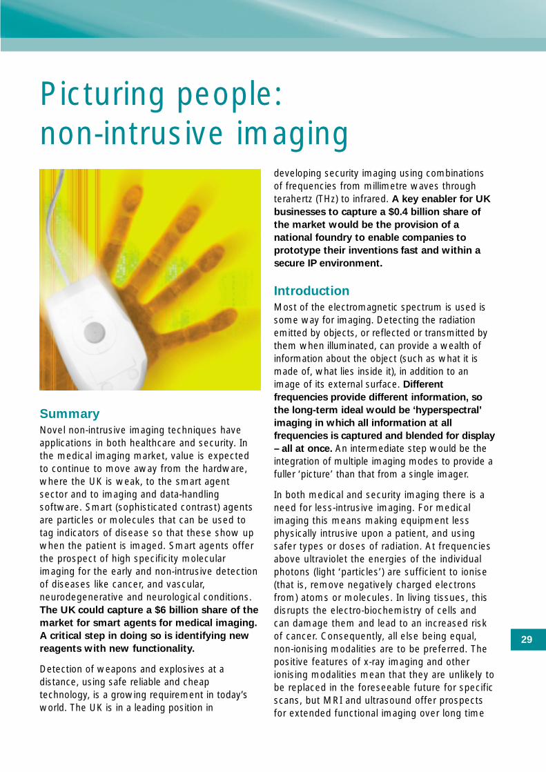
29
Summary
Novel non-intrusive imaging techniques haveapplications in both healthcare and security. Inthe medical imaging market, value is expectedto continue to move away from the hardware,where the UK is weak, to the smart agentsector and to imaging and data-handlingsoftware. Smart (sophisticated contrast) agentsare particles or molecules that can be used totag indicators of disease so that these show upwhen the patient is imaged. Smart agents offerthe prospect of high specificity molecularimaging for the early and non-intrusive detectionof diseases like cancer, and vascular,neurodegenerative and neurological conditions.The UK could capture a $6 billion share of the
market for smart agents for medical imaging.
A critical step in doing so is identifying new
reagents with new functionality.
Detection of weapons and explosives at adistance, using safe reliable and cheaptechnology, is a growing requirement in today’sworld. The UK is in a leading position in
developing security imaging using combinationsof frequencies from millimetre waves throughterahertz (THz) to infrared. A key enabler for UK
businesses to capture a $0.4 billion share of
the market would be the provision of a
national foundry to enable companies to
prototype their inventions fast and within a
secure IP environment.
Introduction
Most of the electromagnetic spectrum is used issome way for imaging. Detecting the radiationemitted by objects, or reflected or transmitted bythem when illuminated, can provide a wealth ofinformation about the object (such as what it ismade of, what lies inside it), in addition to animage of its external surface. Different
frequencies provide different information, so
the long-term ideal would be ‘hyperspectral’
imaging in which all information at all
frequencies is captured and blended for display
– all at once. An intermediate step would be theintegration of multiple imaging modes to provide afuller ‘picture’ than that from a single imager.
In both medical and security imaging there is aneed for less-intrusive imaging. For medicalimaging this means making equipment lessphysically intrusive upon a patient, and usingsafer types or doses of radiation. At frequenciesabove ultraviolet the energies of the individualphotons (light ‘particles’) are sufficient to ionise(that is, remove negatively charged electronsfrom) atoms or molecules. In living tissues, thisdisrupts the electro-biochemistry of cells andcan damage them and lead to an increased riskof cancer. Consequently, all else being equal,non-ionising modalities are to be preferred. Thepositive features of x-ray imaging and otherionising modalities mean that they are unlikely tobe replaced in the foreseeable future for specificscans, but MRI and ultrasound offer prospectsfor extended functional imaging over long time
Picturing people: non-intrusive imaging
30
periods, for example, throughout an operation.Ultrasound is of course not an electromagneticspectrum technology, although it has to beconsidered as a competing technology in the marketplace.
Security scanning of people cannot use ionisingradiation for safety reasons (x-ray scanners atairports are used only for baggage). Less-intrusive imaging has obvious advantages inbeing more covert, and less disruptive topassengers at airports, for example. An exciting
new area with great promise for security
imaging is THz radiation, which lies between
microwaves and visible light and can provide
spectroscopic information to identify
substances, as well as images of concealed
items. Use of the THz part of the spectrum hasbeen hampered by the absence of cheapsources and efficient detectors. Recentbreakthroughs, led by the UK, are now openingup opportunities for THz applications, which maywell extend beyond the security sector.
Medical imaging
Key drivers
Greater demand for healthcare, particularly foran increasingly aged, and affluent, population, iswidely recognised as a critical driver in society.
Within the drive towards better healthcare thereare a number of broad trends. The desire to
minimise the negative side-effects of
healthcare, and the growing requirement to
image patients for extended periods during
treatment and screen for predisposition to
disease, provide strong motivation towards
less-invasive imaging methods. Surgerycarries its own set of risks, particularly ofinfection. Keyhole surgery has replaced manymajor surgical interventions; improved imagingoffers the prospect of reducing the need forbiopsies and other investigative operations.
Ionising radiation (x-rays, PET, SPECT and gammaray scans) cause damage to cells that can lead tocancers. There is thus a drive towards using non-ionising imaging modalities, such as MRI, wherepossible, and reducing dosages where there is noalternative to ionising imaging modalities.
In seeking to improve treatment capability, ahigh priority is placed on combating the bigkillers, including oncological, vascular,neurodegenerative and neurological diseases.High specificity and high sensitivity imagingplays a central role in the early detection ofdisease and in monitoring the effects of therapy.In due course it could also become integratedinto highly controlled guided therapy systemsusing feedback from real-time diagnosticmonitoring. It might also find a market formental state monitoring of the growing numberof people who suffer depression at some stageof their life.
Another key driver in healthcare is equality ofaccess. Many advanced treatments and diagnostictools are currently only available at specialistcentres. This provides a drive to cheaper, morecompact imaging devices that do not require aspecialist to operate or interpret them.
The action group considered that within thecontext of non-intrusive imaging, the drivers inhealthcare led towards two key market areas:high specificity and molecular imaging fordisease detection by specialists; and low-cost
flexible imaging devices for primary healthcare centres.
High specificity and molecular imaging
Markets and applications
High specificity imaging plays a central role in
the early detection of diseases such as cancer
by identifying molecular signals of disease.
The development of continuous monitoring wouldenable the effects of therapy, or a patient’smental state, to be tracked, and drug type anddosage adjusted accordingly. In the longer term,diagnostics and treatment could be integratedinto therapy systems in which feedback from real-time diagnostic monitoring would controlhighly-personalised therapy.
The most promising way of delivering high
specificity non-intrusive imaging lies in the
use of smart agents with an imaging
modality such as MRI, PET or x-rays. Smart(sophisticated contrast) agents are particles or

31
Picturing people: non-intrusive imaging
molecules that enable specific indicators ofdisease to show up when the patient is imaged.Contrast agents are passive tags that can beseen at all times, whereas smart agents haveactive features – for example, they may only‘switch on’ once attached to the target. Long-term goals for very smart agents involve activetransmission of information rather than simpleimaging of location. Although improvements inimaging hardware alone might deliver improvedspecificity, for example, better tissuerecognition, imaging at the molecular level islikely to require smart tagging for theforeseeable future.
The principal components of a smart agent highspecificity imaging system are: the imaginghardware; the data analysis software; and thetagging agents through which indicators ofdisease are identified. At present, about 60% ofthe value of the market lies in the hardware, butthe value of this sector is declining relative toagents and data analysis. The group estimatedthat in 15 years’ time 50% of the value of theoverall market would lie in smart agents.
In assessing the market for smart agents, theaction group considered that detection of cancer,vascular and neurodegenerative/neurologicaldiseases would form the major part of themarket. Their ‘best guess’ estimate was for acombined market value of $25 billion in around15 years’ time, with the relative sizes of themarkets for these three diseases being 40% oncology, 30% vascular and
30% neurodegenerative/neurological. The groupnoted that, although detection of diabetes wasalso a potential application, alternative detectiontechnologies were already established so theprospects for smart agents were less certain inthe face of such competition. The UK has a
strong presence in the smart agent market
(Amersham plc) so the group estimated that
the UK might expect to take 25–35% of this
market (if Amersham plc remain based in this country).
The initial stage of the R&D process is relativelylong, probably academic rather than industrial,and will involve trying a number of avenues toachieve proof of concept identification of a newagent with novel functionality. This would befollowed by a short commercial proof of conceptphase, which may include adding new functionalcomponents into the imaging equipment tomaximise the efficacy of the new agent. The keymilestone at the end of a lengthy (about 8 years)phase three is approval from the US FederalDrugs Agency (since around 45% of the marketis in the US), although European Union approvalis also important. One-off manufacturing start-upcosts are relatively low because the productionprocesses established during development arelikely to be adequate for the productionvolumes. The R&D process is the same for eachdisease although initial investment costs will behigher for neurological agents because of theextra difficulties associated with transmissionacross the blood–brain barrier.
Table 6. Market estimates for smart agents
Investment costs – three R&D phases plus one-off pre-production costs
Phase 1 Phase 2 Phase 3 Pre- Total Value of World UK shareInitial (duration) (duration) production investment UK share marketinvestment (duration) cost (total of market(duration) duration)
Best guess $160 million $50 million $1.2 billion $75 million $1.5 billion $6 billion $25 billion 25%of UK (5 years) (2 years) (8 years) (1 year) (16 years)market size
Optimistic $13 billion $37 billion 35%market size(20% likelihood)

32
The principal risk to the UK investing in this
area is that of GE pulling Amersham plc out
of the UK (but the new GE Healthcare
business will be headquartered in the UK).
Setting that aside, the UK’s research and
business strengths in this field and the
relative confidence of this as a growing
market make this a less uncertain proposal
than some others considered by the project.
Technologies
Identifying new smart agents with the
desired functionality is the key technological
development. Passing all the regulatory trialsand gaining approval for their use is the most expensive step. In the longer term,development of more generic nanotags withtransmission capabilities would permit ever-more intelligent imaging.
Dual modality instuments (such as PET/CT) areavailable now. Fully multispectral imaging, fusingdata from multiple modalities, is a long-termgoal. Sophisticated data analysis and fusionsoftware is essential.
Low-cost flexible imaging
Markets and applications
Earlier detection of disease does not dependonly on better-quality imaging, it also dependson patient access. Improving the imagingcapabilities available at point of entry into thehealthcare system would enable doctors tomake earlier, more accurate, diagnoses.
The challenges in addressing the primary
healthcare-centre imaging market are not
about new technologies but about
engineering current ones to be cheaper,
more compact and easier to use. The size ofthe market for these devices will depend on anumber of other infrastructure enablersincluding: high-bandwidth telephony for datatransmission to and from experts; skills andeducational provision at the local level; and cleardata protection, and automated decision-making,regimes that are accepted by the public andprofessionals alike.
The action group agreed that only certainimaging modalities were suitable for movingdown the healthcare chain, from specialistcentres to all hospitals and/or from them on toprimary healthcare centres. The groupdiscounted any significant future market formodalities involving radioactive isotopes inprimary healthcare centres on safety/securitygrounds. It was agreed that the modalities ofultrasound and (digital) x-rays offered the bestprospects for meeting the demands of thismarket in the short term. MRI was thought tobe significant in the longer term, but requiresmore to be done by way of development tomeet the specifications of the market. A keyrequirement is ease of use: if equipment is tobecome commonplace in primary healthcarecentres it must not require a specialist tooperate or to interpret the data. Smart softwarefor data and image analysis is thus critical,although this will need to be combined withlocal training.
Because addressing the production aspects ofthis market is in the main about refining theengineering of existing products, existingsuppliers clearly have a great advantage. The UKhas very little presence in this sector and thegroup concluded that whilst the market wassignificant (they estimated the size of the digitalx-ray market alone for primary healthcarecentres at $45 million in 5 years’ time) therewas little chance of the UK capturing anyworthwhile part of this market. The UK has
strengths in software and image analysis
development, which form component parts
of the overall market. The group felt that theseoffered good entrepreneurial opportunities forsmall-scale businesses but any such ventureswere likely to be bought out by larger overseasequipment manufacturers if successful.
Technologies
As with high resolution high-end imaging,
sophisticated data analysis and fusion
software is essential for low-end low-cost
imaging. Imaging software has in recent yearsbeen driven by the entertainments industry:there was no clear consensus on whether

33
Picturing people: non-intrusive imaging
NO
W5
ye
ars
10
ye
ars
15
ye
ars
TechnologiesApplicationsC
ell s
tate
an
d t
ype
pro
filin
g Imag
er –
spat
ially
con
tro
lled
th
erap
y
Co
nti
nu
ou
s p
ers
on
al
thera
py m
on
ito
rin
g
• tr
ackin
g e
ffect
of
th
era
py a
nd
do
sag
e
• live m
on
ito
rin
g
o
f p
ers
on
al d
osag
e
Imag
ing
n
euro
tran
smitt
ers
–h
igh
ly s
elec
tive
fun
ctio
nal
imag
ing
Valid
atio
n o
f flu
ore
scen
t m
arke
rs (r
egu
latio
n m
ay
del
ay b
y 7
year
s)
Iso
top
e o
n
dem
an
d m
ore
easily
Sm
art m
ole
cule
s/m
ole
cula
r as
sem
ble
rP
assiv
e
nan
ob
ots
wit
h
tran
sm
itte
r
to a
llo
w
rem
ote
trackin
g
Gen
eral
sm
art
tag
gin
g:
•ce
ll m
ob
ility
to
tra
ck c
ells
•
link
to a
ny
anti
bo
dy
or
met
abo
lic
mar
ker
Men
tal h
ealt
h
mo
nit
or:
•
rese
arch
ass
essm
ent
• ea
rly
dia
gn
ose
s t
o r
edu
ce im
pac
t (
e.g
. Par
kin
son
’s)
Dis
tin
gu
ish
ing
can
cers
fr
om
no
rmal
tu
mo
urs
Tum
ou
r m
ole
cula
r m
arke
r im
agin
gIm
agin
g v
uln
erab
le p
laq
ue
Sp
ott
ing
ab
no
rmal
dis
ease
Reg
ula
tory
en
viro
nm
ent
slo
w
and
exp
ensi
ve
Dete
cta
ble
nan
ota
gg
ing
(gen
eri
c)
PE
T a
nd
fu
sio
n
of
imag
ing
En
do
sco
pe
mo
difi
catio
ns
to s
po
t flu
ore
scen
t m
ater
ials
Act
ive
nan
ob
ots
Web
sca
n
ho
me
dev
ice
imag
er
Op
tical
im
agin
g
sho
rt-p
uls
e O
CT
Mu
ltid
isci
plin
ary
team
– a
ssem
bly
d
iffi
cult
Dat
a fu
sio
n;
anal
ysis
/ au
tom
ated
d
ecis
ion
Figure 7. Non-intrusive imaging: technology timelines for high specificity and molecular imaging.(key steps shown in orange)
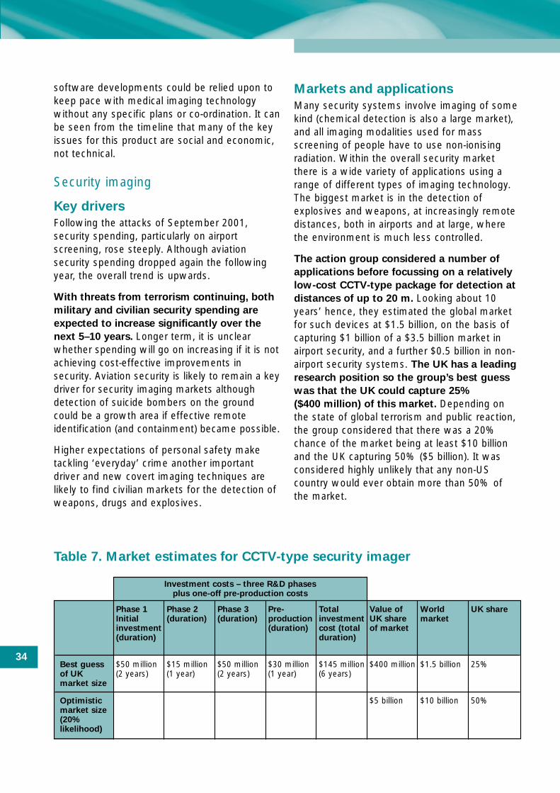
34
software developments could be relied upon tokeep pace with medical imaging technologywithout any specific plans or co-ordination. It canbe seen from the timeline that many of the keyissues for this product are social and economic,not technical.
Security imaging
Key drivers
Following the attacks of September 2001,security spending, particularly on airportscreening, rose steeply. Although aviationsecurity spending dropped again the followingyear, the overall trend is upwards.
With threats from terrorism continuing, both
military and civilian security spending are
expected to increase significantly over the
next 5–10 years. Longer term, it is unclearwhether spending will go on increasing if it is notachieving cost-effective improvements insecurity. Aviation security is likely to remain a keydriver for security imaging markets althoughdetection of suicide bombers on the groundcould be a growth area if effective remoteidentification (and containment) became possible.
Higher expectations of personal safety maketackling ‘everyday’ crime another importantdriver and new covert imaging techniques arelikely to find civilian markets for the detection ofweapons, drugs and explosives.
Markets and applications
Many security systems involve imaging of somekind (chemical detection is also a large market),and all imaging modalities used for massscreening of people have to use non-ionisingradiation. Within the overall security marketthere is a wide variety of applications using arange of different types of imaging technology.The biggest market is in the detection ofexplosives and weapons, at increasingly remotedistances, both in airports and at large, wherethe environment is much less controlled.
The action group considered a number of
applications before focussing on a relatively
low-cost CCTV-type package for detection at
distances of up to 20 m. Looking about 10years’ hence, they estimated the global marketfor such devices at $1.5 billion, on the basis ofcapturing $1 billion of a $3.5 billion market inairport security, and a further $0.5 billion in non-airport security systems. The UK has a leading
research position so the group’s best guess
was that the UK could capture 25%
($400 million) of this market. Depending onthe state of global terrorism and public reaction,the group considered that there was a 20%chance of the market being at least $10 billionand the UK capturing 50% ($5 billion). It wasconsidered highly unlikely that any non-UScountry would ever obtain more than 50% of the market.
Table 7. Market estimates for CCTV-type security imager
Investment costs – three R&D phases plus one-off pre-production costs
Phase 1 Phase 2 Phase 3 Pre- Total Value of World UK shareInitial (duration) (duration) production investment UK share marketinvestment (duration) cost (total of market(duration) duration)
Best guess $50 million $15 million $50 million $30 million $145 million $400 million $1.5 billion 25%of UK (2 years) (1 year) (2 years) (1 year) (6 years)market size
Optimistic $5 billion $10 billion 50%market size(20% likelihood)
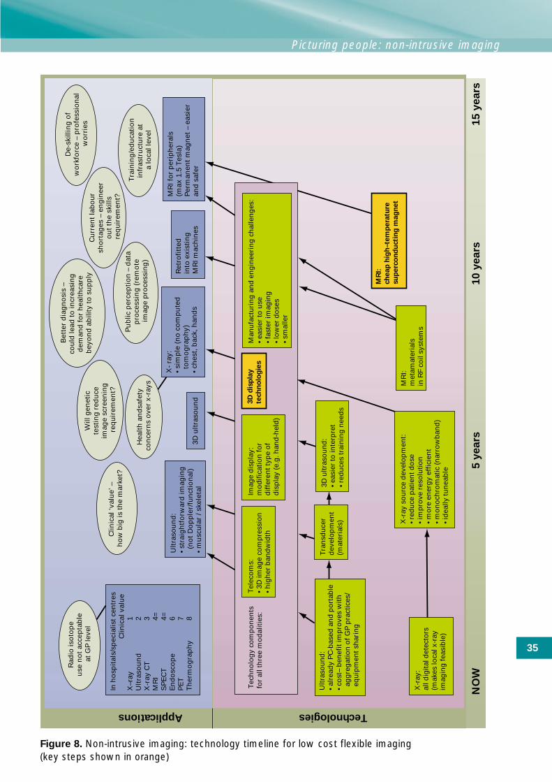
Picturing people: non-intrusive imaging
35
NO
W5
ye
ars
10
ye
ars
15
ye
ars
TechnologiesApplications
MR
I fo
r p
erip
her
als
(max
1.5
Tes
la)
Per
man
ent
mag
net
– e
asie
ran
d s
afer
X-
ray:
• si
mp
le (
no
co
mp
ute
d
to
mo
gra
ph
y)•
ches
t, b
ack,
han
ds
Ret
rofi
tted
in
to e
xist
ing
M
RI m
ach
ines
In h
osp
ital
s/sp
ecia
list
cen
tres
Clin
ical
val
ue
X–r
ay
1U
ltra
sou
nd
2
X-r
ay C
T
3M
RI
4=
SP
EC
T
4=E
nd
osc
op
e
6 P
ET
7T
her
mo
gra
ph
y
8
Clin
ical
‘val
ue’
–
ho
w b
ig is
th
e m
arke
t?P
ub
lic p
erce
pti
on
– d
ata
pro
cess
ing
(re
mo
te
imag
e p
roce
ssin
g)
Cu
rren
t la
bo
ur
sho
rtag
es –
en
gin
eer
ou
t th
e sk
ills
req
uir
emen
t?
De-
skill
ing
of
wo
rkfo
rce
– p
rofe
ssio
nal
w
orr
ies
Tra
inin
g/e
du
cati
on
infr
astr
uct
ure
at
a lo
cal l
evel
Ult
raso
un
d:
• st
raig
htf
orw
ard
imag
ing
(
no
t D
op
ple
r/fu
nct
ion
al)
• m
usc
ula
r / s
kele
tal
3D u
ltra
sou
nd
MR
I:
ch
eap
hig
h–te
mp
era
ture
su
perc
on
du
cti
ng
mag
net
Rad
io is
oto
pe
use
no
t ac
cep
tab
le
at G
P le
vel
Will
gen
etic
te
stin
g r
edu
ce
imag
e sc
reen
ing
re
qu
irem
ent?
Bet
ter
dia
gn
osi
s –
cou
ld le
ad t
o in
crea
sin
g
dem
and
fo
r h
ealt
hca
re
bey
on
d a
bili
ty t
o s
up
ply
3D
dis
pla
y
tech
no
log
ies
Man
ufa
ctu
rin
g a
nd
en
gin
eeri
ng
ch
alle
ng
es:
• ea
sier
to u
se•
fast
er im
agin
g•
low
er d
ose
s •
smal
ler
Imag
e d
isp
lay:
mo
difi
catio
n fo
r d
iffer
ent t
ype
of
dis
pla
y (e
.g. h
and
-hel
d)
Tel
eco
ms:
• 3D
imag
e co
mp
ress
ion
• h
igh
er b
and
wid
th
Tec
hn
olo
gy
com
po
nen
ts
for
all t
hre
e m
od
aliti
es:
MR
I:m
etam
ater
ials
in R
F co
il sy
stem
s
Ultr
aso
un
d:
• al
read
y P
C-b
ased
an
d p
ort
able
• co
st–
ben
efit
imp
rove
s w
ith
ag
gre
gat
ion
of G
P p
ract
ices
/ e
qu
ipm
ent s
har
ing
X-r
ay:
all d
igita
l det
ecto
rs(m
akes
loca
l x-r
ay
imag
ing
feas
ible
)
Tra
nsd
uce
r d
evel
op
men
t (m
ater
ials
)
3D u
ltras
ou
nd
:•
easi
er to
inte
rpre
t•
red
uce
s tr
ain
ing
nee
ds
X-r
ay s
ou
rce
dev
elo
pm
ent:
• re
du
ce p
atie
nt d
ose
• im
pro
ve r
eso
lutio
n•
mo
re e
ner
gy
effic
ien
t•
mo
no
chro
mat
ic (n
arro
wb
and
)•
idea
lly tu
nea
ble
Hea
lth
an
dsa
fety
co
nce
rns
ove
r x-
rays
Figure 8. Non-intrusive imaging: technology timeline for low cost flexible imaging(key steps shown in orange)

36
The first phase of R&D would provide proof ofconcept for the technology and components.The second would demonstrate commercialviability – integration and manufacture – and thethird would produce final prototypes. Pre-production costs depend on whether the UKbuilds a mass-production foundry: for their ‘bestguess’ figure the group assumed some kind offactory share. To capture the optimistic 50%share of the market a dedicated UK foundrywould be needed. Compared to some of theother proposals considered by the project, theinitial investment costs are higher, with themiddle phases being the cheaper ones althoughit is still an attractive option. To reap big benefitswill, however, require both a prototyping and amass production foundry.
Technologies
There are very many imaging technologies toconsider in meeting the needs of securitymarkets, and most are likely to find a use insome particular niche application. For example,vapour spectroscopy could be important forremote detection of volatile substances, andthermal detectors are likely to continue to beused in low-resolution short-range applications.
Even for the entry-level CCTV-imager marketthere are a number of different specificelectromagnetic technologies that could meet thespecification for this device. The imaging radiationis likely to be in the millimetre wave to THz toinfrared range, where the resolution is good andsubstances may be identified by spectroscopy.Penetration, particularly in wet weather, can be anissue if these devices are to be used outside.
Technology developments are particularly
needed to produce cheap reliable detectors: it
is likely that there will be a move away from
the current Indium Phosphide (InP) detectors
to silicon. Because of this, the group felt that thedevelopment of a UK, or EU, silicon R&D foundryto enable rapid prototyping of designs wasessential for the UK to build on its presence inthis market.
In the longer term, discrete imaging units will beincreasingly combined into hybrid systems,possibly using data at many frequencies and
integrated on-chip (at least 20 years out). Aswith other topics, image analysis and processingsoftware is critical to the development ofsophisticated surveillance systems.
The way forward
The UK has the opportunity to develop a
significant market share in:
• smart agents for use in high specificity
medical imaging
• non-intrusive security imaging using
frequencies from millimetre waves through
THz to infrared.
The UK could capture a $6 billion market insmart agents for disease detection. The UK hasthe scientific expertise and, in Amersham plc, an industry leader well placed to exploit thisopportunity. The challenge is to support UKbusiness to maintain their position and stay inthe UK.
A critical step in capturing markets is the
identification of new smart agents. To ensure
this happens, we need to further develop the
excellence of imaging science in the UK and
facilitate interdisciplinary research. Support fordevelopment advances needs to be well focused,for example, by: setting up a multi-disciplinaryresearch facility located in a hospital; or runningshort, tightly defined programmes pullingtogether experts from a range of places to solve aparticular challenge. Involving large procurers ofimaging equipment such as the NHS in providingpurchasing support and a buoyant home marketin this technology would also be helpful.
The UK also has a leading technological position innovel security imaging devices and could capturea market value of between $0.4 billion and $5 billion. A particular challenge for growing UK
business in this sector is access to the facilities
needed to test and develop detector
prototypes. Development of either a UK or EU
rapid prototyping silicon foundry is needed,
with clear rules on IP sharing/protection.
Potential government procurement contracts forinnovative technology would also help to supportthe development of a UK-based business aroundthis market.
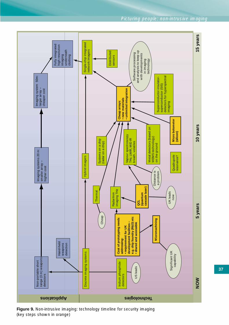
37
Picturing people: non-intrusive imaging
NO
W5
ye
ars
10
ye
ars
15
ye
ars
TechnologiesApplications
Fully
inte
gra
ted
h
igh
res
olu
tio
n
imag
ing
u
nd
ern
eath
cl
oth
ing
Han
d-h
eld
w
eap
on
sd
etec
tio
n
QC
L
(qu
an
tum
cascad
e laser)
Mic
ro b
olo
mete
r
(silic
on
)
Met
al d
etec
tors
(bas
ed o
nM
EM
S te
chn
olo
gy)
o
n th
e g
rou
nd
Vap
ou
r sp
ectr
osc
op
yT
Hz,
LW
IR, M
ID IR
bre
ath
, vo
latil
es
Mic
rom
ach
inin
g
Ch
eap
arr
ays:
• n
ew
mate
rials
• u
nlim
ited
in
teg
rati
on
Imag
ing
sys
tem
50m
: la
rger
arr
ay –
ch
eap
er c
ost
No
n-p
ort
able
sh
ort
ra
ng
e (3
m)
wea
po
ns
det
ecto
rs
UK
lead
s n
ow
Dis
tan
ce is
a
pro
ble
m
US
lead
s
Ch
eap
Imag
ing
sys
tem
s 20
m:
smal
ler
arra
y –
hig
her
co
st
Co
st
of
pro
toty
pin
g n
eed
s
ad
dre
ssin
g:
• re
qu
irem
en
t fo
r U
K
develo
pm
en
t fa
cilit
ies –
e.g
. ch
ip f
ou
nd
ry (
R&
D)
etc
• sh
are
d a
nd
accessib
le
Dis
cret
e im
agin
g s
yste
ms
Ind
ium
ph
osp
hid
ed
etec
tors
Hyb
rid
imag
ers
Sys
tem
s o
n a
ch
ip
(rad
ar o
n a
ch
ip)
Rad
ar/m
m
imag
ing
TH
z
Sin
gle
-ch
ip in
teg
rate
dn
etw
ork
imag
ers
Th
erm
al
Dis
trib
ute
d
sen
sors
Qu
adru
po
lere
son
ance
?
Su
per
con
du
cto
r-in
sula
tor-
sup
erco
nd
uct
or
(SIS
) d
etec
tors
for
hyp
ersp
ectr
al
imag
ing
So
ftw
are
pro
cess
ing
an
d a
nal
ysis
to
kee
p u
p
wit
h d
evel
op
men
ts
in im
agin
gte
chn
olo
gy
Sig
nif
ican
t U
K
cap
abili
ty
Figure 9. Non-intrusive imaging: technology timeline for security imaging(key steps shown in orange)

38
EPSRC, the MRC, the Department of Health
and the CCLRC are exploring ways of
improving multidisciplinary working onmedical imaging and the prospects for a ‘smartagent medical imaging centre’.
Acknowledgements
We would like to thank all members of theaction group who gave so generously of theirtime and expertise.
Dr Brian Allen, e2v Technologies
Professor James Barlow, Imperial College London
Professor Sir Michael Brady, Oxford University
David Burrows, DSTL
Professor David Delpy, University CollegeLondon
Dr Peter Dukes, MRC
Dr Matthew Hogbin, Home Office
Dr Elizabeth Hylton, EPSRC
Mrs Mel King, Department of Health
Dr Ian McDougall, Oxford Instruments
Dr Andrew Mackintosh, Oxford Instruments
Dr Brian Maddison, CCLRC Rutherford AppletonLaboratory
Professor Paul Matthews, Oxford University
Dr Delyth Morgan, MRC
Dr Douglas Paul, Cambridge University
Professor Michael Pepper, CambridgeUniversity/TeraView Ltd
Dr Allyson Reed, QinetiQ
Dr Clifford Smith, Amersham plc
State of the science review author: Dr Douglas Paul, Cambridge University

Printed in the UK on recycled paper with a minimum HMSO score of 75. Department of Trade and Industry. © Crown Copyright. www.dti.gov.uk DTI/Pub 7250/1k/04/04/. URN 04/856