experimental investigation of open-ended microwave oven ... · experimental investigation of...
TRANSCRIPT

Experimental Investigation of Open-Ended Microwave Oven Assisted Encapsulation Process
S.K. Pavuluri1, M. Ferenets2, G. Goussetis3, M. P. Y. Desmulliez1, T. Tilford4, R. Adamietz5, G. Muller5, F. Eicher5 and C. Bailey4
MIcrosystems Engineering Centre (MISEC), School of Engineering and Physical Sciences, Heriot-Watt University, Edinburgh EH14 4AS, Scotland, United Kingdom
Tel: +44 (0)131-451-3774, E-mail: [email protected], [email protected]
2 Eesti Innovatsiooni Instituut OÜ Sepapaja 6, 11415 Tallinn, Estonia
3The Institute of Electronics, Communications and Information Technology (ECIT), Queen’s University Belfast, NI Science Park
Queen’s Road, Queen’s Island, Belfast, BT3 9DT
4 University of Greenwich Computing and Mathematical Sciences
Park Row, Greenwich, London SE10 9LS, UK
5Fraunhofer Institut für Produktionstechnik und Automatisierung, Stuttgart, Germany
Abstract An open ended microwave oven is presented with
improved uniform heating, heating rates and power conversion efficiency. This next generation oven produces more uniform EM fields in the evanescent region forming part of the heating area of the oven. These fields are vital for the rapid and uniform heating of various electromagnetically lossy materials. A fibre optic temperature sensor and an IR pyrometer are used to measure in situ and in real-time the temperature of the curing materials. An automatic computer controlled closed feedback loop measures the temperature in the curing material and drives the microwave components to obtain predetermined curing temperature cycles for efficient curing. Uniform curing of the lossy encapsulants is achieved with this oven with typical cure cycle of 270 seconds with a ramp rate of 1oC/s and a hold period of 2 minutes. Differential scanning calorimeter based measurement for the pulsed microwave based curing of the polymer dielectric indicates a ~ 100% degree of cure.
Introduction Diffusion or laminar flow based convection ovens are
conventionally used to cure thermosetting polymer dielectric materials intended for the packaging of microelectronic devices. The primary requirements for such curing equipment include uniform temperature distribution, good control of heat rate and the provision of adequate ventilation to remove volatiles that are released during the curing process [1]. These conventional thermal processing/curing steps can last for several hours slowing throughput and thus increasing the cost of manufacturing. As the demand for lighter, faster, and more compact electronic and MEMS devices increases, there is a need for innovative material processing techniques that reduce packaging time and increase throughput. Considerable effort has been focused on the use of electromagnetic radiation such as gamma rays, ultraviolet (UV) light, and electron beam accelerators for curing polymer dielectric materials. Gamma radiation is formidable while electron
beam radiation is not cost effective and has limited throughput. UV light has poor penetration for thicker polymer materials and current equipment has low intensity at wavelengths that are useful for processing these materials. These limitations have prompted a number of research groups recently to investigate the use of microwave radiation to cure polymeric dielectrics [2-5]. Microwave heating of polymers is a volumetric heating process in which strong dipole group’s couple to the microwave field. The conversion of electric field into heat is proportional to the frequency, the dielectric loss, and the electric field strength. Investigations into microwave curing of epoxy and encapsulant resins are well documented. Early publications include research into the heating of epoxy resins using waveguides [2, 3] and multi-mode waveguide cavity ovens [4, 6]. Waveguide based ovens have been employed to investigate temperature versus time curing profiles for epoxy utilizing a pulsed input source.
A microwave heating technique, VFM (Variable Frequency Microwave) has been considered recently for the rapid curing of both conductive and non conductive based polymer dielectrics [7-10]. The VFM based curing investigations have shown higher cure rates and curing at reduced temperatures as compared with the conventional curing processes [7]. The processed packaging materials have shown reduced residual stresses as well as an increase in adhesion to the metal tracks and substrate compared to conventionally cured samples [11]. Theoretically, VFM heating can reduce curing durations by as much as 6 to 10 times compared to convection heating [1]. Rapid sweeping across a wide bandwidth of microwave frequencies produces a uniform energy distribution through the oven chamber as a result of the heavy overmoding. The duration of the frequency sweep, of the order of 100 ms, reduces the likelihood of arcing, thus allowing in principle the microwave heating of metals and semiconductor without any damage.
The novel open end microwave oven presented in this article can be employed to process materials similar to
those submitted to VFM based curing. A primary advantage of this oven is the potential for further integration with a pick and place machine to achieve simultaneous fine placement and curing where as conventional microwave and VFM based ovens are often bulky and impractical for their integration with a precision placement machine. The possibility with this oven to be placed onto a pick and place machine allows also the individual curing of components on a PCB board, an attractive technological proposition for rework and the assembly of low-thermal budget devices. Productivity gains arise from the considerable simplification in a production line process due to the direct placement of the target into the heating chamber, which avoids the need for physical opening and closing of the heating chamber. The oven has an overall weight of less than 0.5 kg. It is advisable that the volume of the curing epoxy material to be inserted in the open ended oven must not be more than 10% of its open end volume and should be close to the dielectric insert at the open end [12-16]. This will reduce EM (Electro - Magnetic) radiation from the open end of the oven and also keeps the perturbation of the operating frequency of the oven to a minimum.
The open ended oven is driven by a microwave source coupled with additional microwave components that include a TWT (Traveling Wave Tube) amplifier, a power meter and an isolator. Microwave based pulsing techniques are employed to produce uniform EM fields for effective curing/heating of the materials involved. This novel oven can potentially be manufactured at different cross-sectional dimensions for curing/heating of the materials of different dimensions and shapes. The applications for the open end oven include heating, curing, photoresist baking, microwave welding, annealing of various materials essential for the packaging of microelectronic devices. On the other hand, conductive based pastes that are lossy before curing such as ICA’s can be cured by utilizing the pulsing capability of the system. Moreover, the proposed design is also suitable for selective heating within a large substrate, which can be useful particularly when the latter includes parts sensitive to stresses induced by the high temperatures involved [8,17-18].
Design of Improved Open Ended Microwave System
A. Open Ended Oven
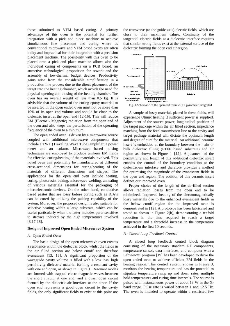
The basic design of the open microwave oven creates a resonance within the dielectric block, whilst the fields in the air filled section are below cutoff and therefore evanescent [13, 15]. A significant proportion of the waveguide cavity volume is filled with a low loss, high permittivity dielectric material forming a resonant cavity with one end open, as shown in Figure 1. Resonant modes are formed with trapped electromagnetic waves between the short circuit, at one end, and a quasi open circuit formed by the dielectric-air interface at the other. If the open end represents a good open circuit to the cavity fields, the only significant fields to exist at this point are
the transverse (to the guide axis) electric fields, which are close to their maximum values. Continuity of the tangential electric fields at a dielectric interface requires that similar strong fields exist at the external surface of the dielectric forming the open end air region.
Fig. 1.Schematic of the open end oven with a pyrometer integrated
A sample of lossy material, placed in these fields, will experience Ohmic heating if sufficient power is supplied. Adjustment of the source power, longitudinal position of the target package within the air filled section, impedance matching from the feed transmission line to the cavity and target package material will dictate the optimum length and degree of cure for the material. An additional ceramic insert is embedded at the boundary between the main or bulk dielectric filling (PTFE based substrate) and air region as shown in Figure 1 [12]. Adjustment of the permittivity and length of this additional dielectric insert enables the control of the boundary condition at the dielectric-air interface and therefore provides a method for optimising the magnitude of the evanescent fields in the open end region. The addition of this ceramic insert defines our improved oven.
Proper choice of the length of the air-filled section allows radiation losses from the open end to be minimized. Improved heating of the electromagnetically lossy materials due to the enhanced evanescent fields in the below cutoff region for the improved oven is demonstrated in [12]. A prototype has been fabricated and tested as shown in Figure 2(b), demonstrating a tenfold reduction in the time required to reach a target temperature and a threefold increase in the temperature achieved in the first 10 seconds.
B. Closed Loop Feedback Control
A closed loop feedback control block diagram consisting of the necessary standard RF components, temperature sensor, data interfaces, and computer with a Labview™ program [19] has been developed to drive the open ended oven to achieve efficient EM fields in the heating region. This control system, shown in Figure 3, monitors the heating temperature and has the potential to stipulate temperature ramp up and down rates, multiple hold temperatures and curing time intervals. The source is pulsed with instantaneous power of about 13 W in the X-band range. Pulse rate is varied between 1 and 12.5 Hz. The oven is intended to operate within a restricted few

frequency modes to reduce the complexity of the required wide band amplifiers.
(a)
(b)
Fig. 2. Photograph of (a) pick and place machine (b) open end oven integrated with placement machine
A fibre optic temperature thermometer, the Neoptix™ Reflex™ signal conditioner and an IR pyrometer are used to record the temperature distribution within the curing sample and provides the basis for a closed loop control routine [20]. The digital signals from these devices are interfaced to the computer via RS-232 communication interface for logging the temperature output. The fibre optic sensor itself is a GaAs based sensor fed with an optical fibre that is protected by polyimide tubing. The sensor tip is protected with silica gel filled into the polyimide tubing. The fibre sensor itself is inserted into a ceramic ferrule of about 2.7 mm in diameter for further protection during the temperature measurement phase. A typical cure profile consists of a ramp up period, a hold period and a ramp down period. Monitoring of the curing of the materials can be achieved by (a) measuring the temperature at about 100 millisecond time intervals in the material, (b) comparing this temperature with a programmed temperature profile and (c) pulsing the microwave source accordingly.
C. Numerical Analysis of Polymer Cure Kinetics
Rigorous numerical treatments are necessary for the study of the coupled thermal and electromagnetic energies during the curing processes. In order to enable the in-situ assessment of material cure, a number of models have been developed which estimate the degree of cure through the numerical integration of a complex function of time and material temperature. An overview of the modeling of the curing process is presented by Morris et al. [21]. These models are used to obtain the required cycle temperature profiles for the curing of the material with the open end microwave oven.
Curing Investigation
A. Principle
The amount of microwave power transferred per unit volume (Wm-3) into the curing material with an open end oven is given by
∫′′
=V
res dVEEV
fP *.
rrεπ
where fres is the resonant frequency of the coupled mode, ε ′′ is the imaginary component of the complex
permittivity, Er
is the electric field and V is the volume of the material. In order to maximise the dielectric power loss and therefore the heating potential, the target sample should have a high dielectric loss tangent relative to the dielectric filling (bulk) materials within the cavity. If the dielectric loss of the bulk filling material is high, then unwanted heating within the material will occur.
B. Test Samples Glob top IC packaging is investigated with the novel
open ended oven. The encapsulant used in the study is EO1080 produced by the Company Henkel. This is a one component epoxy resin highly filled with silica based filler and carbon additives for improved microwave absorption. The test specimen consists of an adhesive injected on to the cover slips or PTFE film of 8 mm × 8 mm dimensions and a thickness of about 1 mm. The overall thickness of the sample varies between approximately 1 mm and 1.5 mm. The variation in test sample volume has a negligible impact on the electromagnetic performance of the cavity as the perturbation of the resonant frequency for each mode or mode set is very small. The complex permittivity of the encapsulant has been measured at room temperature using a dielectric probe and was found to have a relative permittivity of 5.025 and loss tangent of 0.25 at 8.2 GHz.
Fig. 3 Block diagram of the microwave components necessary to drive the open end microwave oven
A temperature profile has been specified according to the recommended datasheet of the paste manufacturers. The cavity is excited by a coupling probe located centrally within the transverse plane on the copper end wall. A target temperature versus time is plotted over a period of 300 s. The source is pulsed automatically such that the average temperature of the sample corresponds to that of the target temperature. The source frequency is manually adjusted to ensure that the cavity is excited at resonance

with a net instantaneous power flow of atleast 13 W during the course of the heating experiment. The resonant frequency is detuned by approximately 0.5% at peak temperatures. This is attributed to the power absorbed by the PTFE, causing variation of its complex permittivity as a result of the change in temperature. The evolution over time of temperature rise has been studied for the epoxy based encapsulant dielectric material in terms of various cure times and pulse rates. The specimens are cured with the open end oven presented in [12] and the rise in temperatures are measured with a fibre optic temperature thermometer and an IR pyrometer.
C. Characterization of post cure specimens
The cure kinetics of polymer dielectrics for a conventional oven has initially been carried out using the Differential Scanning Calorimetric (DSC) method. A series of curing tests have been performed on the encapsulant material in order to find out the influence of the cure temperature cycle on the cure development as well as the resulting degree of cure. From these results, a temperature profile is estimated that is applicable for the microwave assisted curing of these materials with the open end oven. The net RF power input into the encapsulant can be defined as the power obtained after the power losses inside the bulk filling (PTFE and ceramic insert) and connector losses less the net power flow measured by the power sensor.
DSC analysis was performed using a Perkin Elmer DSC-7 device to study the curing behavior of the no-flow encapsulant polymer material. Measurements were performed in nitrogen at a flow rate of 20 ml/min. Aluminum crucibles with volume of 50 µl were used. In order to avoid possible pressure generation caused by solvents evaporation a small hole was made into each sealed crucible. Photographs of the cured polymer materials are shown in Figure 4. The degree of cure was calculated by comparing the change in enthalpy (Delta H) for conventionally full cure and the Delta H measured from the microwave cured samples as shown in Figures 8 and 9.
Results Figure 5 shows an infrared temperature of the curing
encapsulant profile with the open end microwave oven where the red region corresponds to the curing encapsulant material. It can be seen from the photograph that there is sufficient distribution of temperature in the encapsulant material. An LM2940C-12 voltage regulator chip has been encapsulated in a QFN package by curing with the improved oven system and successfully tested for functionality
Figure 6 shows the measurement results of the microwave power input into the encapsulant and the measured fibre optic temperature curves for a 150oC curing cycle with a pulsed source. The amount of RF power input changes with time. The net microwave power input into the oven is measured at 100 ms time intervals. The measured temperature follows the programmed
temperature until the hold period at 240 seconds. The measured ramp down temperature is not consistent with the requested ramp as the test specimen does not have an active cooling system to cool the samples at an accelerated rate.
A two stage pulsing method is employed in order to follow the set programmed temperature profile. The microwave source is pulsed at a rate of about 12.5 Hz during the ramp up period for 100 s and a pulse rate of about 5.5 Hz during the hold period from 100 s to 160 s of the curing cycle. Although the source is in the on-state long after the temperature reaches 150oC, not much energy is input into the encapsulant. This can be attributed to the change in complex permittivity of the material with temperature or the exothermal cure reaction of the material.
Fig. 5 IR (Infrared) temperature profile for the encapsulant material heated with the open ended oven
Fig. 6 Measurement results of the microwave power into the
encapsulant and the temperature curves for a 150oC curing cycle
Figure 7 shows the measurement results of the microwave power into the encapsulant and the measured fibre optic temperature curves for an 180oC curing cycle. The amount of RF power input again changes with time.
(a)
(b)
Fig. 4 Photograph of the cured polymer material measured with (a) fibre optic sensor and (b) with a pyrometer

The measured temperature follows the programmed temperature for 115 seconds during the ramp up period. The hold period for this cure cycle is 60 seconds.
The measured hold temperature is not consistent with
the programmed temperature after 115 seconds. This behaviour can be attributed to the change in complex permittivity of the material with temperature or with phase change of the material. The microwave source is pulsed at a rate of about 12.5 Hz during the ramp up period for 100 s and a pulse rate of about 5.5 Hz during the hold period from 100 s to 160 s of the curing cycle.
Fig. 8 DSC curve for cured E01080 encapsulant material cured at
150oC
Figure 8 shows the elimination of the exothermal peak
(DSC) for a microwave cured EO1080 encapsulant specimen with a 98% degree of cure for the 150oC cure cycle. Figure 9 shows the elimination of the exothermal peak (DSC) for a microwave cured EO1080 encapsulant specimen with an 81% degree of cure for the 180oC cure cycle. The lower degree of cure of the polymer material for the 180 oC cure cycle can be attributed to the smaller hold period of 60 s as opposed to 120 s for the 150oC cure cycle. Figure 10 shows the measurement results of the IR pyrometer measured temperature curves for a 150oC curing cycle with a pulsed source. A one stage pulsing
method is employed in order to follow the set programmed temperature profile with a pulse rate of 1 Hz.
Fig. 10 Measurement results of the temperature curves for a 150oC
curing cycle with the encapsulant material
Fig. 11 Measurement results of the temperature curves for a two
step 150oC curing cycle with the encapsulant material
Table 1 Comparison of different curing cycles
Temperature (oC)
Measurement
Pulsing (Hz)
Degree of cure
Time (s)
150 Fibre optic thermometer
12.5 and 5.5
98% 270
180 Fibre optic thermometer
12.5 and 5.5
81% 180
150 Pyrometer 1 100% Tg is
113 oC 270
Two step: 115 and 150
Pyrometer 1 Closer to 100%
Tg is 100 oC
270
Figure 11 shows the measurement results of the IR pyrometer temperature curves for a 150oC two stage curing cycle with a pulsed source. A single stage pulsing method is employed in order to follow the set programmed temperature profile with a pulse rate of 1 Hz. A lower pulse rate will increase the net RF power flow into the curing material. Table 1 compares the measurement methods and the cure cycles by degree of cure achieved. The table shows that complete curing is achieved with lower pulse rate but without any reduction of overall cure time of 270 seconds. The samples cured at lower pulse rate also showed improved curing along the material circumference edges. Glass transition temperature (Tg) is considered to be a sensitive probe for the degree of cure beyond 95% wherein the regular DSC curves cannot predict a complete cure of the material [22]. The higher the Tg, the closer is the degree of cure to 100%. It can be observed from the table that a single step temperature profile had resulted in a higher degree of cure when compared to a two step temperature profile for the same pulse rate and curing time.
Fig. 9 DSC curve for cured E01080 encapsulant material cured at 180oC
Fig. 7 Measurement results of the RF power into the encapsulant and the temperature curves for a 180 oC curing cycle

Conclusions An improved open ended microwave oven is presented
for glob top IC packaging. Implementation of this oven for IC packaging and for other types of packaging requires reliable control over the frequency, power and uniformity of EM fields and an understanding of cure models for the different materials involved. This open end microwave oven is optimised for the lower order modes of operation for curing polymer dielectrics. The optimised dielectric insert in the open end oven increases the rate of heating by a factor of more than ten over the observable temperature range. Pulsing technique tends to control the temperature of the curing material quite accurately. The microwave power required to maintain the curing material at a predefined temperature varies with time. High ramp rates can also be implemented with sufficient hold intervals. No significant visible residual stresses are observed at the edges of the encapsulant sample. The change in complex permittivity of the material with temperature or with phase change of the material is observed. The measured temperature curves do not follow the predicted cure temperature models based on the conventional heating techniques. This can be primarily due to the method used for temperature measurement and also can be due to the low temperature curing capability of the VFM based oven [10].
Acknowledgments The authors wish to acknowledge funding and support
from the European Union Framework 7 programme (FP7-SME-2007-2), contract number 218350 and additional support from our partners, Kepar Electronica S.A., Camero di Commercio Industria, Artigianato e Agricoltura di Milano, Mikrosystemtechnik Baden-Württemberg e.V., the National Microelectronics Institute, ACI-ecotec GmbH & Co. KG, Industrial Microwave Systems Ltd. and Ribler GmbH.
References
1. Ghosh, M. K and Mittal, K. L, Polyimides: Fundamentals and Applications. New York: Marcel Dekker, 1996.
2. Gourdenne, A, "Possible Use of the Microwave in Polymer Science," Int. Conf. on Reactive Processings of Polymers Proc., pp. 23-30, 1982.
3. Karmazsin, E and Satre, P, "Use of Continuous and Pulsed Microwave for Quick Polymerization of Epoxy Resins," Thermochimica Acta, vol. 93, pp. 305-308, 1985.
4. Strand, N. S, "Fast Microwave Curing of Thermoset Part," Modern Plastics, vol. 57, pp. 64-67, 1980.
5. Wang, Y.-J. et al, "Microwave Cure of Metal-Filled Electrically Conductive Adhesive," IEEE Electronic Components and Technology Conference, pp. 593-597, 2001.
6. Wilson, L. K and Salerno, J. P, "Microwave Curing of Epoxy Resins," Technical Report, vol. AD-A067 732, 1978.
7. Hubbard, R. L and Garard, R. S, "Wafer Level Curing of Polymer Dielectrics with Variable Frequency Microwaves," presented at Advanced Thermal
Processing of Semiconductors, 2007. RTP 2007. 15th International Conference on, 2007.
8. Glinski, G. P, and Bailey, C, "Microwave Cure of Conductive Adhesives for Flip-Chip & Microsystems Applications," IEEE InterSociety Conf. on Thermal Phenomena, pp. 848-853, 2002.
9. Alford, T. L. et al, "Variable Frequency Microwave Induced Low Temperature Dopant Activation in Ion Implanted Silicon," presented at Advanced Thermal Processing of Semiconductors, 2009. RTP '09. 17th International Conference on, 2009.
10. Davis, C. E and May, G. S, "Neural Network Control of Variable-Frequency Microwave Processing of Polymer Dielectric Curing," Electronics Packaging Manufacturing, IEEE Transactions on, vol. 31, pp. 104-113, 2008.
11. Tanaka, K. et al, "Variable Frequency Microwave Curing of Amide-Epoxy Based Polymers," Components and Packaging Technologies, IEEE Transactions on, vol. 30, pp. 472-477, 2007.
12. Sinclair, K. I. et al, "Optimization of an Open-Ended Microwave Oven for Microelectronics Packaging," IEEE Trans. MTT, vol. 56, pp. 2635-2641, 2008.
13. Sinclair, K. I. et al, "Open Ended Microwave Oven for Packaging," Symposium on Design, Test, Integration and Packaging of MEMS/MOEMS, DTIP 2008, Nice, France, pp. 16-20, 2008.
14. Sinclair, K. I. et al, "Advanced Microwave Oven for Rapid Curing of Encapsulant," in 2nd Electronics System integration Technology Conference, 2008, pp. 551-556.
15. Sangster, A. J. et al, "Open-Ended Microwave Oven for Flip-Chip Assembly," IET Microwave and Antennas Propag., vol. 2, pp. 53-58, 2008
16. Sinclair, K. I. et al, "Open-Ended Microwave Oven for Flip-Chip Assembly," IEEE Proc. European Microwave Conference, pp. 620-623, Amsterdam, The Netherlands, 2007.
17. Noh, H.-S. et al, "Wafer Bonding using Microwave Heating of Parylene Intermediate Layers," Journal of Micromechanics and Microengineering, vol. 14, pp. 625-631, 2004.
18. Noh, H.-S. et al, "Wafer Bonding using Microwave Heating of Parylene for MEMS Packaging," IEEE Electronics Packaging Tech. Conf., pp. 924-930, 2004.
19. "National Instruments. http://www.ni.com/labview/," Dec. 2008.
20. "Neoptix Inc, T1 Fibre optic temperature sensor", http://www.neoptix.com/literature/v1002_Datasheet_t1.pdf.
21. Morris, J. E. et al, "Polymer Cure Modeling for Microelectronics Applications", Proceedings of 32nd International Spring Seminar on Electronics Technology (ISSE 2009), Brno, Czech Republic, 2009.
22. Zhang, Z and Wong, C.P, “Study and Characterizations on the Post Cure Behavior of Underfill” Proceedings of 9th Int’l Symposium on Advanced Packaging Materials, pp. 208-214, Atlanta GA, March, 2004.