experimental investigation of new device test structures...
TRANSCRIPT
Experimental investigation of new device test structures for determiningthe lifetime in solar cells
Rufat Alizada, Lis Nanver, Javid Aliyev and Ray HuetingDepartment of Semiconductor Components, University of Twente, Enschede, The Netherlands
(emails: [email protected], [email protected])
Abstract— Octagonal ring-shaped test structures have beendeveloped for experimental investigation of charge carrier flowsin p-type regions configured as the emitter of a vertical pnptransistor. An I-V characterization of the test structures isperformed to evaluate their suitability for investigating theelectrical performance of emitters for n-type crystalline solarcell in terms of surface recombination and minority carrierlifetimes. The emitter regions in this study are formed byusing pure boron (PureB) depositions under different processingconditions. The base current, ideally formed by injection ofelectrons into the emitter, is found for the region of interest byusing a differential measurement technique. For solar cells, theemitter should preferably be designed to suppress the injectionof electrons as much as possible. Differences in the emitterefficiency between the fabricated emitters are identified andrelated to the method of processing.
Index Terms— c-Si solar cells; surface recombination; bipolartransistor test structure; PureB diodes; emitter efficiency; sheetresistance
I. INTRODUCTION
As worldwide energy demands increase, conventionalenergy resources such as fossil fuels, will be exhaustedwithin the next century. Therefore development and usageof alternative energy resources is important, especially ifwe could use the long-term natural resource of the Earth-the sun. Solar cells are considered to be a major candidatefor obtaining energy from the sun, since they can convertlight to electricity [1]. The figure of merit for conversionperformance of a solar cell, built using a semiconductorphotodiode, is efficiency, which depends on the minoritycarrier lifetime. This is basically the average time that acarrier can spend in an excited state after electron-holegeneration before recombining.
In silicon, photodiode solar cells consist of highly-dopedp- or n-type emitter, an n- or p-type base as junctionlayers, metallic contacts, dielectric layers as silicon surface-passivation and anti-reflection coatings [2]. The interfacesbetween the silicon and contacting/passivation layers havein common that they are a major source of interface statesfor generation/recombination of charge carriers. In bulkimpurities and other defects of the crystal structure can be asource of generation/recombination of carriers but often thesurface effects dominate. Characterising the carrier lossesin the solar cell is considered to be complicated task, asit is generally not possible to disentangle its two maincomponents, recombination in the bulk and at the surface.
Surface recombination and lifetime in silicon devices havebeen studied and lots of different approaches have beenproposed [3]-[7]. However, in the proposed measurementtechniques, the presence of carrier trapping and surfacerecombination can have a strong effect on the measuredresponse time, causing it to be much larger that the actuallifetime and therefore unable to give accurate values forcalculating the efficiency [8].
In this study, new test structures are investigated withthe objective of separately measuring the hole and elec-tron current flows in p-type emitter regions to evaluate theinfluence of surface recombination on the lifetime of thecarriers. Additionally, in this work a pure boron (PureB)layer was used for creating the p+region and a number ofdifferent processing procedures are examined that may beof interest for fabricating c-Si solar cells. PureB has alreadybeen extensively studied as a means of creating the p+ regionof ideal p+n diodes with junction depths down to a fewnanometers [9], [10]. The advantage of these diodes is thatdespite having a shallow junction depth, reverse currentsin the diodes are the same low level as for conventionaldeep junction diodes. This low-leakage property has beenaccorded to the fact that a high effective hole concentration iscreated at the PureB-to-Si interface, thus giving an efficientsuppression of electron injection from the n-region and acorrespondingly low saturation current [11],[12].
In the present test structures, the PureB is incorporated asthe emitter in a bipolar transistor structure. The design allowsto study both emitter contact regions where metal is placeddirectly on the p+ region and emitter passivation regionsin which dielectric is deposited on the p-region. By usingdifferent test-structure geometries and a differential measure-ment technique, the minority carrier electron injection intothe emitter can be determined for each region of interest.In a solar cell, the electron injection must be minimizedsince only holes should be collected at the anode and allelectrons should travel through thick n-region to the cathode,which requires an electron lifetime that is as long as possible.The bipolar test structures allow to separately optimise theelectron injection in each region of the emitter, somethingthat is not possible with only a simple diode structure.
II. TEST STRUCTURES
The basic p+np bipolar structures studied in this work areshown in Fig. 1. The starting substrates were <100> 1-10
1

Ohm p-type Si wafers that were first thermally oxidized toa silicon-dioxide (SiO2) layer thickness of 200nm. Throughthis layer, the n-type base region and the n+ contacts regionswere formed by implantation and thermal activation. Win-dows to the Si were then opened where the PureB depositionwas to be performed. Before this deposition, shallow p+-regions were implanted and activated at 700C as an initialpart of the PureB deposition cycle. Four different types ofdevices with a variety of deposition temperatures, depositiontimes and metallization methods are studied here. Two ap-proaches were taken for metallization of the diodes. In thefirst approach, shown in Fig. 1a, a 0,6µm PECVD SiO2 wasdeposited on top of the PureB. Contact windows to the n+
and p+ regions were then etched on this oxide and Al/1%Siwas sputtered and patterned to form the metal contact pads.In this way, an emitter region that is covered with oxide isformed in the region between contacts. This resembles howan emitter region passivated by a dielectric could be madein solar cell as shown in Fig. 2. Fig.1b illustrates secondmetallization approach where the devices are metalized bycontacting the whole PureB emitter region with the depositedAl/Si. This resembles the emitter contacting regions of solarcell also indicated in Fig. 2. The processing parameters ofthe four PureB emitter types studied in this work are listedin Table I.
Fig. 1. Cross section of the test structures with two different metallizationmethods: (a) fabrication of the central oxide window by Al-contacting thediode through a ring-shaped window to the PureB at the perimeter of thediode, and (b) contacting the whole emitter region by depositing Al directlyon the PureB.
TABLE IPROCESSING PARAMETERS FOR THE 4 PUREB EMITTER REGIONS.
Device NamePureB
Deposition Anneal/oxidationat 950C
Depositionof 0.6µmPECVD
Simulatedjunction
depth(nm)Temp(C) Time(min)
HT6 700 6 no yes 5
HT20 700 20 yes yes 400
LT20 400 20 no no 0
LT40 400 40 no no 0
Fig. 2. Schematic cross-section of a typical concept of an n-type siliconbased solar cell with a front emitter. The indicated emitter passivating layerand front contact can be studied using the test structures of respectivelyFig.1a and Fig.1b [13].
Octagonal-ring shaped bipolar structures are designed withthe purpose of extracting parameters related to the laterallyuniform part of the emitter region by subtracting peripheralcontributions, associated with the collector and base regions,from the measurements. Sets of octagon-shaped structureswere designed with a fixed 65µm radius to the center ofthe emitter ring, so that total perimeter is always fixedindependent of the length of the octagon rings. Sets of each8 octagon ring structures are designed as in Fig. 3. with thering width L equal to 23,7µm, 24µm, 25µm, 26µm, 28µm,30µm, 34µm and 64µm. This gives a fixed perimeter of2x431µm.
Fig. 3. Octagon-ring shaped structures with ring width.
The PureB layer that is used here to form the p emitter canhave two functions in this respect. As a more conventionalfunction, the layer acts as a source of a boron dopants, whichdiffuse into silicon up to the solid solubility, which is about2 ·1019/cm3 at 700C [14].
The test structures HT6 and HT20 have two p+ rings(inner and outer contacts) which are connected together bya thin PureB layer that dopes the Si at 700C. In HT20 thePureB layer was oxidized after deposition at a temperatureof 950C. The oxidation cycle was designed to completelyconsume the pure boron layer and give a doping of the Siwith a peak value of 2 ·1020/cm3 at the surface [10]. In thisdevice the central emitter region is therefore expected to beoxide covered p-Si.
The function of the PureB is less conventional for LT20and LT40 devices. The p-type region is not formed bydoping of the Si, since the deposition temperature of 400Cis too low for this. Nevertheless, a p+-region is formeddue to an interface reaction between the pure boron andthe Si surface. In this reaction, it has been proposed thata monolayer of fixed acceptor is formed that attracts amonolayer of holes to the interface[15]. This layer of holeshas been shown to be as efficient in suppressing the electroninjection as a deep p+ diffused region.
2

The implanted p+ region is expected to have a deeperjunction depth than the PureB-only region. This means thatthe depletion of the n-type base will be larger under thep+ region, which in turns means that the base width issmaller. The smaller the width the higher the resistance. Thisis indicated in Fig. 4.
Fig. 4. A schematic cross section of the pnp test structure. The width ofthe base region is narrowed as a result of change in depletion region causedby implanted p+ contact regions.
III. METHOD
PureB diodes are known for property of functioning as pnjunctions with very low saturation current despite junctiondepths down to a few nanometers [10]. This is attributedto the formation of a monolayer of holes at the PureB-to-Si interface [15]. Without this hole layer, the total holeconcentration from B-doping of the Si, equivalent to ashallow diffused junction, is limited at 700C and the B-doped region forms an almost transparent layer for electroninjection from the n-substrate [9], [11]. Therefore, when themetal covers the diode’s surface, the IV characteristics aredetermined by the electron injection into the metal [16].Moreover, imperfections at the interface with the metal willoften be a source of generation-recombination (g-r) currentsthat deteriorate both electrical and optical performance. ThePureB diodes give a way of avoiding these problems whilestill maintaining a nm-shallow junction.
The best way to experimentally study the electron andhole currents through a diode is to separate them by using abipolar structure. In our case, p+np structures with the PureBdepositions used to form the emitter allow us to do that. Insuch structures, a forward voltage is placed over the emitter-base junction so that high electron and hole currents flowthrough the junction. The holes are injected from the emitterinto the base that is so narrow that practically all the holesare swept to the collector by electric field over the reverse-biased collector-base junction depletion region as shown inFig. 5.
Fig. 5. Electron (blue) and hole (red) current flow in an pnp transistorbiased to operate in the active mode. The base current is the sum of thehole diffusion current IE,p, the base recombination current, Ir,B and the base-emitter depletion layer recombination current, Ir,d .
If there are defects in the base region, some of the injectedholes may recombine there. For each hole that recombinesin the base region, another electron enters the base as basecurrent (IB). This gives the parasitic g-r base current indicatedin Fig. 5. Since the p+np bipolar structure is designed to havea high collector current and low base current, even a smallg-r current can be observed as an increase in base current.Eventually, the I-V characteristics of the test structures werestudied using Gummel plots, where the base current IB wasobserved. Three different measurements were performed onthe HT6 and HT20 devices. Basic cross section of the devicesand the schematic of the measurements are illustrated in Fig.6. Fig. 6a depicts biasing over two emitters, while measuringbase (IB) and collector (IC) currents. IBE2
and IBE1base
currents are measured while outer E2 and inner E1 emittersare biased respectively.
Fig. 6. Schematic cross section of HT20 and HT6 devices with (a) bothemitters connected, (b) only inner emitter E2 is connected and (c) outeremitter E1 is connected. The base current(IB, IBE2 , IBE1 ) is in all casesmeasured under forward bias.
Another parameter that may be extracted out of thestructures and contribute to the characterization is the sheetresistance (Rsh). Rsh may be extracted out of the resistancemeasurements of outer and inner octagonal ring structureswhich later on have to be corrected by radial correctionfactor.
A. Gummel NumberTo gain insight in the current flows in the different types
of junction we first look at the ideal case, disregardingdefect-induced currents. The electron and hole currents overa junction can be expressed as [1]:
I = qn2i0A · ( 1
GD+
1GA
) · (eqVkT −1) (1)
Ih =qn2
i0AGD
· (eqVkT −1) (2)
Ie =qn2
i0AGA
· (eqVkT −1) (3)
3
where q is elementary charge, ni0 is the intrinsic carrierconcentration, A is the diode area, GD and GA are Gummelnumbers of the n and p-doped regions and kT/q is thethermal voltage.
The electron injection into the emitter region is governedby the Gummel number GA of the region. In general formu-lation this can be defined as [1]:
GA =∫
WQNA
NE(z) ·n2i0
Dn(z) ·n2ie
dz+NA
SA
n2i0
n2ie
(4)
where WQNA is the width(or depth) of the p-type doped
region, nie(z) = ni0e(−4EG(Z)
2kT ) is the effective intrinsic carrierconcentration,4EG(z) is the bandgap difference with respectto the c-Si, NA is the active p-type doping concentration,Dn(z) is the electron diffusion coefficient in the p-region asa function of depth z from Si surface, and SA is the surfacerecombination velocity.
In first instance, it can be useful to consider the ideal case,but many diodes will have I-V characteristics that deviatefrom the ideal case due to, e.g., defect-related parasiticcurrents and series resistance. To stretch the applicability ofthe basic Eq. (1), the ’ideality factor’ was introduced in thedenominator of the exponential term.
B. Ideality Factor
For actual non-ideal diodes, the expression for the I-Vbehaviour is often written as in Eq. (5). The parameter n inthis equation is the ideality factor.
I = Io · (eqVnkT −1) (5)
Having Gummel plots and knowing the values of k, T andq, the ideality factor may be easily calculated. Typically, Sidiodes have an n between 1 and 2, the latter being seenwhen g− r currents dominate [1],[17]. PureB diodes can befabricated with high ideality and often have an n below 1.02[18].
C. Sheet Resistance of the Emitter Regions
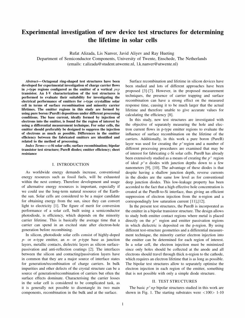
To determine the sheet resistance Rsh, a differential mea-surement technique is applied as described in [20]. In thismethod the resistance associated with the contacts are elim-inated and the real value of sheet resistance of the layer ofinterest can be extracted. Sets of octagonal ring structuresare designed with the basic design illustrated in Fig. 7.Each octagonal ring structures has a fixed perimeter length,therefore only two variables are important for the sheetresistance extraction. These are the measured resistance, Rmiof each measured structure and the ring length Li, where theindices i = 1, ...,n refer to each specific test structure in thegiven set of n structures (section II). Since the structures areoctagon-ring shaped, the radial spreading must be taken intoaccount [19].
Fig. 7. Schematic cross section (a) and layout (b) of the octagonal ringsheet resistance measurement structure. The perimeter of the PureB-onlyregion is constant and equal to 2x431µm while the length of the octagonalring has varying values Li.
If the length of the ring is very small compared to radiusrg, rg >> Lj ≈ Li the Rsh can be determined as
Rij = Rmj−Rmi = Rsh ·Lj−Li
W(6)
When the Li is of the same order as rg, then the radialspreading of the current from the inner contact to outercontact of the ring must be taken into account. For anoctagonal ring a radial correction factor can be calculatedas,
Rmj−Rmi = Rsh ·αij (7)
and
αij =1
6,627ln[
(rg−0.5 ·Li)(rg +0.5 ·Lj)
(rg +0.5 ·Li)(rg−0.5 ·Lj)] (8)
where αij is the proportionality that relates Rij to Rsh.Plotting Rij versus the calculated values of radial correc-
tion factors must provide a linear relation and the value ofthe extracted sheet resistance [19].
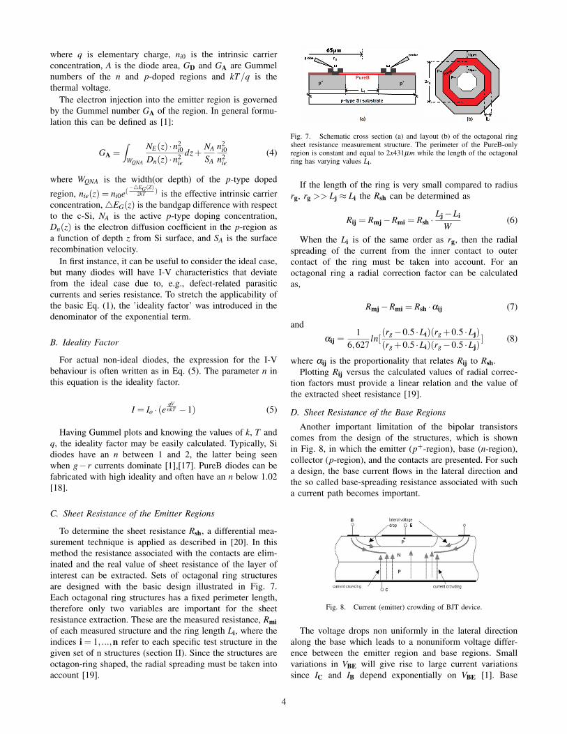
D. Sheet Resistance of the Base Regions
Another important limitation of the bipolar transistorscomes from the design of the structures, which is shownin Fig. 8, in which the emitter (p+-region), base (n-region),collector (p-region), and the contacts are presented. For sucha design, the base current flows in the lateral direction andthe so called base-spreading resistance associated with sucha current path becomes important.
Fig. 8. Current (emitter) crowding of BJT device.
The voltage drops non uniformly in the lateral directionalong the base which leads to a nonuniform voltage differ-ence between the emitter region and base regions. Smallvariations in VBE will give rise to large current variationssince IC and IB depend exponentially on VBE [1]. Base
4

spreading resistance results in the so-called emitter-currentcrowding at the edges of the emitter region and reducesconduction at the center of the emitter region.
Fig. 9. Schematic cross section of the LT40 and LT20 devices used forthe base resistance measurements.
A different set of test structures were available for mea-suring the sheet resistance of the base in the HT6 and HT20devices in the regions, where (1) no emitter, (2) a PureB-only region emitter, and (3) a p+ region is formed. Thebase sheet resistance of the LT20 and LT40 devices canbe determined by I-V measurements over two base contactregions illustrated in Fig. 9. Eventually, a differential mea-surement technique is applied to correct measured resistancewith radial proportionality factor as described in [20].
IV. RESULTSA. I-V Characteristics
The I-V characteristics of the HT6 device with an emitterarea of 26x431µm2 are plotted on a semi-logarithmic scaleas indicated in Fig. 10. The hole injection (∼ IC) from the p+
PureB emitter region is separated from the electron current(∼ IB) by collecting the hole current at the collector terminal.The diode displays uniformly low reverse current and anideality factor n=1. The collector current increases exponen-tially in the range 0.2V to 0.7V. Below 0.2V the reversecurrent dominates and above the 0.7V the series resistancein either the base or emitter attenuates the exponential trend.Along with collector current, the base current at low voltagesbelow about 0.2V is dominated by a leakage current thatcould originate from g-r effects at defects in the emitter-basespace-charge or base regions. The leakage current is low atintermediate voltages, slope shows that n≈ 1 just as it is forthe collector current. At higher voltages the curve deviatesfrom exponential growth due to series resistance.
Fig. 10. Gummel plots of HT6 26x431µm2 (L= 26µm) device showingthe effects of emitter-base space charge region recombination(n≈ 1,5−2),quasi-neutral region recombination(n≈ 1), and series resistance.
The I-V characteristics of HT20 device structure is com-pared to the nonanneled device HT6 in Fig. 11. Base currentsIBE2
and IBE1are measured on HT20 and HT6 devices and
plotted in Fig. 11. Both base currents of HT20 and HT6devices display low reverse current and an ideality factor n=1. Below 0.2V the reverse current dominates and above 0.7Vthe series resistance determines the current. Base currents ofHT6 device IBE2
and IBE1identically increase exponentially
in the range 0.2V to 0.7V. Distinction of these base currentsabove 0.7V could be explained by the difference in seriesresistance, which is attributed to the difference of emitterperimeters, as outer emitter has larger perimeter that theinner one. On the other hand, base currents measured forannealed HT20 device were observed to be different overwhole measurement range. In order to observe this strangeeffect, differential IBE2
and IBE1for HT20 device were plotted
against different emitter lengths(Fig. 12).
Fig. 11. Gummel plots of IBE2 , IBE1 and IB as a function of forward biasfor HT6 device (red) and a HT20 (blue). The area of measured emitter is30x431µm2 (L= 30µm).
The linear growth of differential IBE2and linear decline
of differential IBE1in Fig. 12, illustrate that the measure-
ments were performed over the whole perimeter and thatin the PureB-only region there was no p-type region to befound. This could be explained by an excessive oxidationof the PureB region during the oxidation/anneal step. This,however, is in contrast to the results obtained in reference[10] where the procedure is shown to deliver a highly-dopedp-region of about 0,3µm deep as shown in Fig. 13.
Fig. 12. Measured IBE2 and IBE1 of HT20 device for various active emitterlengths.
5

Fig. 13. ECV-measured active boron concentration profiles of variousinitially deposited PureB layers, followed by thermal annealing at 950Cfor 10-min in 14% O2 concentration [10]. Sheet resistance of these profilesare also included in the legend.
Fig. 14. Measured IBE2 and IBE1 of HT6 device for various active emitterlengths.
Fig. 14 illustrates differential IBE2and IBE1
for HT6device plotted against different emitter lengths. The minordifference between IBE2
and IBE1is observed for small values
of L. With the increase in length of active emitter region, thedifference in base currents increases. This could be explainedby the radial spreading of the current in the octagonal-ringstructures.
Fig. 15. IBE2 at 450mV forward bias for HT6 and HT20 diodes measuredfor various active emitter lengths.
In order to compare the HT6 and HT20 over the activeemitter region, differential IBE2
currents at 0.4V were plottedversus different emitter lengths. The HT6 devices resulted
in higher base current that HT20 devices. Higher basecurrent of the nonannealed HT6 device can be explainedby surfaces with an interfaces containing a large numberof recombination centers because of the abrupt terminationof the semiconductor crystal forming efficient recombinationcenters.
Typical Gummel plots measured on the LT20 and LT40devices are shown in Fig. 16. At low processing tempera-tures, the lack of a high-temperature anneal step is often aproblem because defects introduced during processing arenot removed by thermal diffusion processes. In the two LTdevices the shorter deposition time of 20 min for the LT20devices resulted in about 3 decades higher base current thanthe LT40 devices. Moreover, as shown in Fig. 17, there is adecade higher spread of the base current measured at 0.4 Vforward bias for the LT20 devices. These differences betweenthe two device types do not show any geometry dependenceas is demonstrated by Fig. 17 where the IB is compared fordevices with L = 1, 2, 4, 6, 10 and 40 µm.
Fig. 16. Gummel plots of the base current as a function of forward bias forLT20 (red) and LT40 (blue). The area of the measured emitter is 10x431µm2
(L= 10µm).
Fig. 17. Diode current spread at 0.4V forward bias for LT20 and LT40diodes with different areas. Measurements are performed on dies 1 and 2(shown inset) and 2 diodes per area are measured per die.
Base currents of three different emitters contacted directlyby metal were compared with respect to their efficiencyfor suppressing the electron injection (Fig. 18). In order
6

to observe injection of currents in the region of interest,differential base currents illustrated in Fig. 18 are plottedagainst active emitter length. 4IB of HT6 is the lowestamong compared devices, which means that Gummel numberof the HT6 emitter is the lowest one (section III A). This isexpected since, emitter region of the LT20 and LT40 devicesis covered with the metal. The suppression of electroninjection in LT40 is found to be more efficient than LT20devices. This shows that different emitter processing mayaffect the injection of electrons into the emitter region.Due to an experimental misfortune, emitters with dielectricpassivation were not available so the effect of recombinationalong the dielectric interface could not be studied.
Fig. 18. 4IB of LT20, LT40 and HT6 devices at 0.5V bias plotted versusactive emitter length.
B. Sheet Resistance of the Emitter Regions
The sheet resistance of the central emitter region of theHT6 structure was extracted from resistance measurementsof a set of octagon-ring structures as shown in Fig. 3.The differential measured resistance values taken betweenstructures with different emitter lengths are plotted in Fig.19 and they display a linear relation between resistance andlength. This indicates that a correct extraction of the PureBemitter Rsh can be made. In Fig. 20 the αij are plottedagainst Eventually, in order to extract Rsh of the PureB,calculated αij were plotted against Rij. The Rij and αij areseen to be linearly correlated, and an Rsh equal to 17,5kΩ/is extracted.
Fig. 19. Subtracted resistance Rij plotted against subtracted active emitterlayer length Lij.
Fig. 20. Subtracted resistance Rij plotted against radial correction factorαij.
For the HT20 structures, it was not possible to measurethe resistance between E1 and E2. I-V measurements of thecurrent through E1 and E2 also indicated that there was nop-type region to be found Fig.12.
C. Sheet Resistance of the Base Regions
The base sheet resistance values measured for the LT20and LT40 devices are listed in Table II. The only differencebetween these structures is the way the emitter is processed.There is no boron doping in the Si, therefore it is notexpected that the neutral base width is different.
TABLE IIMEASURED BASE RESISTANCE FOR DIFFERENT TEST STRUCTURES.
Test Structure Base Resistance
LT20 2,98kΩ/LT40 2,96kΩ/
The sheet resistance of the base region of the HT6 isshown in Table III for the case of with the central PureB-onlyemitter and the peripheral p+-region. At about 2,4kΩ/, thevalues are slightly higher than those of LT devices which isexpected since that the PureB-only emitter is slightly deeperfor the 700C deposition. The Rsh of the p+-region has beenwell-chosen and does not cut off the central base region.Table III also includes the sheet resistance of the base regionwithout any PureB emitter deposition. This gives a base Rshof 1,8kΩ/, which is slightly lower that the HT6 base Rsh.This underlines that the PureB emitter is very shallow.
TABLE IIIMEASURED BASE RESISTANCE FOR HT6 DEVICE.
Test Structure Base Resistance
no PureB emitter 1,78kΩ/PureB-only emitter 2,38kΩ/p+ emitter region 2,43kΩ/
As for the emitter sheet resistance, the base Rsh couldnot be measured for the HT20 device. This suggests thatthe whole central base region has been cut off from then+-contact regions by the anneal/oxidation of the PureBdeposition.
7

V. CONCLUSION
In this paper, pnp bipolar test structures were used toevaluate several types of emitters fabricated using PureBdepositions with respect to their efficiency in suppressingelectron injection from the base region. By using differ-ent test-structure geometries and a differential measurementtechnique the minority carrier electron injection into theemitter was determined for each region of interest. Threedifferent emitters contacted directly by metal were comparedwith respect to their efficiency for suppressing the electroninjection from the base and base leakage currents. Due to anexperimental misfortune, emitters with dielectric passivationwere not available so the effect of recombination alongthe dielectric interface could not be studied. So, futurestudies may be focused on this structures and more detailedanalysis may be performed. Additionally, the differentialmeasurement technique was performed on test structures inorder to extract the sheet resistance of the PureB-only emitterand the base region. Eventually, experimental investigationon the new test structures provided insights on the surfacerecombination of solar cell and eventually proved that theyare suitable for analysing the efficiency of solar cells.
REFERENCES
[1] S.M. Sze and K.K. Ng, ”Physics of Semiconductor Devices”, 3rdedition, John Wiley Sons, Inc., USA, 2007.
[2] ”Solar cell”. Encyclopdia Britannica. Encyclopdia Britannica On-line. Encyclopdia Britannica Inc., 2016. Web. 10 Jun. 2016<http://www.britannica.com/technology/solar-cell>.
[3] F.A. Lindholm, et. al., IEEE Trans. on Electron Devices Vol. ED-34,No. 277, 1987.
[4] A. Neugroschel, ”Determination of lifetimes and recombination cur-rents in p-n junctions solar cells and diodes”, IEEE Trans. on ElectronDevices, vol. ED-28, pp. 108-115, 1981
[5] F. N. Gonzales and A. Neugroschel, ”Measurement of diffusion length,lifetime and surface recombination velocity in thin semiconductorlayers”, IEEE Trans. on Electron Devices, vol. ED-31, pp. 413-415,1984
[6] G. Vitale and P. Spirito, ”Measurement of minority carrier lifetime andinterface recombination velocity in p-i-n diodes from high frequencyresponse of a bipolar JFET device”, Proc. 18th European Solid StateDevice Research Conference, 1988
[7] S.R. Lederhandler and L.J. Giacoletto, ”Measurement of minoritycarrier lifetime and surface effects in junction devices”, Proc. IRE,vol. 3, pp. 477-483, 1955
[8] A.L. Fahrenbruch and R.H. Bube. ”Fundamentals of Solar Cells:Photovoltaic Solar Energy Conversion”. New York: Academic Press,1983. Print.
[9] F. Sarubbi, T.L.M. Scholtes, and L.K. Nanver, ”Chemical vapordeposition of α-boron layers on silicon for controlled nanometer-deepp+n junction formation,” J. Electron. Mater., vol.39, 2, pp.162-173,2010.
[10] K.R.C. Mok, B.W.H. van de Loo, A.H.G. Vlooswijk, W.M.M. Kesselsand L.K. Nanver, ”Boron-Doped Silicon Surfaces From B2H6 Passi-vated by ALD Al2O3 for Solar Cells,” in IEEE Journal of Photo-voltaics, vol. 5, no. 5, pp. 1310-1318, 2015.
[11] F. Sarubbi, L.K. Nanver and T.L.M. Scholtes,”High effective Gummelnumber of CVD boron layers in ultrashallow p+n diode configura-tions,” IEEE Trans. Electron Devices, vol.57, 6, pp.1269-1278, 2010.
[12] L.K. Nanver, A. Sammak, V. Mohammadi, K.R.C. Mok, L. Qi, A.Sakic, N. Golshani, J. Derakhshandeh, T.M.L Scholtes, W.D. de Boer,”Pure dopant deposition of B and Ga for ultrashallow junctions inSi-based devices”, ECS Trans., vol.49, 1, pp. 25-33, 2012.
[13] J. Chen, ”Recent Developments on Silicon Based Solar Cell Technolo-gies and their Industrial Applications, Energy Efficiency Improvementsin Smart Grid Components”, InTech, DOI: 10.5772/59171, 2015.
[14] G. L. Vick and K. M. Whittle, Solid solubility and diffusion coeffi-cients of boron in silicon, J. Electrochem. Soc., vol. 116, no. 8, pp.11421144, 1969.
[15] L. Qi, L.K. Nanver, Conductance along the interface formed by 400Cpure boron deposition on silicon, IEEE Electron Device Letters, vol.36, no.2, pp. 102-104, Dec. 2014.
[16] L.K. Nanver et al., Robust UV/VUV/EUV PureB photodiode detectortechnology with high CMOS compatibility, IEEE J. Sel. TopicsQuantum Electron., vol. 20, no. 6, Nov. 2014, Art. ID 3801711
[17] D.K. Schroder ”Semiconductor Material and Device Characterization”,3rd Ed. J. Wiley, New York, NY, 2006.
[18] X. Liu, L.K. Nanver, ”Comparing Current Flows in Ultrashallow pn-/Schottky-like Diodes with 2-Diode Test Method”,Proceedings ICMTS2016, pp.190 -195, 2016.
[19] L. Qi and L. K. Nanver, ”Sheet resistance measurement for processmonitoring of 400C PureB deposition on Si,” Proceedings of the 2015International Conference on Microelectronic Test Structures, Tempe,AZ, pp. 169-174, 2015.
[20] S.B. Evseev, L.K. Nanver, S. Milosavljevi, Ring-gate MOSFET TestStructures for Measuring Surface-Charge-Layer Sheet Resistance onHigh-Resistivity-Silicon Substrates, Proc. Intl.Conf. on Microelec-tronic Test Structures (ICMTS), Austin, USA, pp.3-8, 2006.
8