experimental demonstration of 4 n 2 classical absorption limit in nanotextured ultrathin solar cells...
TRANSCRIPT
Experimental Demonstration of 4n2 Classical Absorption Limit inNanotextured Ultrathin Solar Cells with Dielectric OmnidirectionalBack ReflectorAndrea Ingenito, Olindo Isabella, and Miro Zeman*
PVMD Laboratory, Delft University of Technology, Dimes, P.O. Box 5053, 2600 GB Delft, The Netherlands
ABSTRACT: The experimental demonstration of the 4n2 classical absorption limit insolar cells has been elusive for the last 30 years. Especially the assumptions on front andinternal rear reflectance in a slab of absorbing material are not easily fulfilled unless anappropriate light-trapping scheme is applied. We propose an advanced metal-free light-trapping scheme for crystalline silicon wafers. For different bulk thicknesses, at the frontside of the wafers we applied a nanotexture known as black-silicon. At the rear side, weimplemented a random pyramidal texture coated with a distributed Bragg reflector.Such a dielectric back reflector was designed to exhibit a maximized omnidirectionalinternal rear reflectance in the region of weak absorption of crystalline silicon.Integrating the measured absorptance spectra of our wafers with the reference solarphoton flux between 400 and 1200 nm, we could calculate the so-called impliedphotogenerated current densities. For wafers thinner than 35 μm, we achieved morethan 99% and up to 99.8% of the implied photogenerated current density based on the theoretical 4n2 classical absorption limit.Successful implementation of our maskless and metal-free light-trapping scheme in crystalline silicon solar cells requires theadequate surface passivation of the front nanotexture. For this purpose we used thermal silicon oxide, but we discuss also theusage of aluminum oxide. Our findings, applied in a solar device structure where front side losses are minimized, open the way forthe realization of next-generation high-efficiency, cost-effective, and ultrathin crystalline silicon solar cells.
KEYWORDS: black-silicon, light in-coupling, optical losses, Tiedje−Yablonovitch limit, Bragg reflector
Light trapping using textured surfaces and metallic backreflector (BR) has contributed to a significant conversion
efficiency gain in crystalline silicon (c-Si) solar cells.1 Forcontinuing large-scale implementation of c-Si solar cells, theirproduction cost must be further lowered by optimizingmanufacturing processes and by using fewer materials withoutsacrificing the efficiency.2−4 Particularly, thinner wafers that arelighter and more flexible5 show a lower bulk recombination6
and exhibit, in the case of Czochralski wafers, a lower light-induced degradation.7,8 However, as c-Si is an indirect band gapsemiconductor, the absorption of the near-infrared region(NIR) of the solar spectrum is significantly reduced in thinnerwafers. Thus light-trapping schemes are essential in thin c-Sisolar cells,9 where light management techniques such as frontlight in-coupling, light scattering, and internal back reflectance(Rb) have to be optimal and concurrently active. Thesetechniques ultimately fulfill the ideal hypotheses of the so-called4n2 classical absorption limit in a dielectric slab,10 where n is thereal part of its complex refractive index: (i) a surface-texturedmorphology at the air/dielectric interface in the role of aperfect broad-band antireflective coating (ARC) (reflectance R= 0 ∀λ), (ii) randomized and ideally diffused light inside theslab (the so-called Lambertian scattering), and (iii) a perfectback reflector (Rb = 1 ∀λ). In the wavelength region of weakabsorption of c-Si (αd < 1), where α and d are the absorptioncoefficient and thickness of the dielectric slab, respectively, such
a light-trapping scheme theoretically results in an absorptionenhancement factor of 50.11
Light trapping in commercial c-Si solar cells is achieved byusing random texturing and metal or a dielectric/metal stack asback reflector. Even though standard random pyramid texturingexhibits a nearly Lambertian scattering,11,12 it does not result ina perfect broad-band antireflective effect. In this respect,nanotextures with feature sizes in the subwavelength range areconsidered valid candidates for providing a broad-bandantireflective effect.13 Among various advanced light-trappingschemes that were lately presented to fulfill the hypothesis ofthe 4n2 classical absorption limit,14−16 a recent opticalsimulation study showed that the absorptance in c-Si canapproach the 4n2 classical limit in a just 2 μm thick structured c-Si slab. Such a slab was endowed with high aspect ratio periodicnanogratings at the front side (FS) for antireflective purposesand with low aspect ratio pyramidal structures at the back side(BS) for efficient long-wavelength light scattering.13 We callthis arrangement decoupled front and rear texturization.17
Based on this design, a c-Si solar cell with a thickness of around9 μm was also reported to achieve a potential photogeneratedcurrent density (JPH) > 36 mA/cm2 and a conversion efficiencyof >7%.18
Received: December 8, 2013Published: February 13, 2014
Article
pubs.acs.org/journal/apchd5
© 2014 American Chemical Society 270 dx.doi.org/10.1021/ph4001586 | ACS Photonics 2014, 1, 270−278
In this contribution we propose an advanced metal-free light-trapping scheme for crystalline silicon solar cells based ondecoupled front and rear textures. Our scheme employs low-cost and industrially scalable processes, such as nanotexturing,also known as black-silicon (b-Si), at FS and random pyramidscoated with a distributed Bragg reflector (DBR) at the BS.19,20
In the following we shall report on our process flow and designsteps for the realization of a dielectric omnidirectional BR.Afterward we shall present our measured c-Si absorptancespectra and compare the performance of dielectric andreference silver BRs with the 4n2 classical absorption limit.Finally, we shall discuss our vision of next-generation c-Si solarcells. In fact our front nanotexture can be efficiently passivatedby using SiO2 grown via dry thermal oxidation21 or by Al2O3deposited via atomic layer deposition (ALD).22 Moreover, ithas been also demonstrated that efficiencies comparable withstate-of-the-art c-Si solar cells can be achieved by using front b-Si texture.21 This opens the possibility to couple our advancedlight-trapping scheme in ultrathin c-Si wafers with efficientpassivation techniques for realizing high-efficiency and cost-effective solar cells.
■ RESULTS AND DISCUSSION
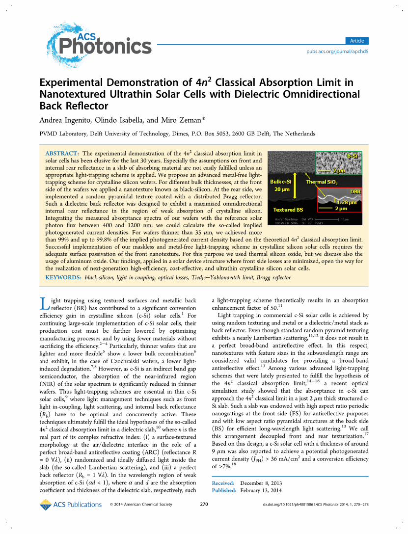
A schematic cross section of the surface textures used in thiswork is illustrated in Figure 1. We realized two thin free-standing absorbing slabs in c-Si wafers that were originally 300μm thick. Both slabs had the same high aspect ratio b-Si FStexture, but the BS was either alkaline-textured with low aspectratio random pyramids (textured BS) or just kept flat (flat BS).The b-Si FS texture was realized with a maskless reactive ionetching (RIE) process, which can be implemented in allcommercially available dry etching tools. The thickness of the
slabs was tuned by varying the etching time as described in theMethods section. We investigated a series of six pairs of slabswith different thicknesses. We measured the thickness of sixslabs in the flat opening to be 190, 140, 100, 80, 40, and 28 μm,respectively. We also noticed that the standard alkaline etchingprocess23 for fabricating the pyramids generally reduced thecorresponding thicknesses of slabs in the textured opening bymore than 5 μm.The atomic force microscopy (AFM) scans of b-Si texture,
random pyramids, and the flat opening are illustrated in Figure1a−c, respectively. The extracted root-mean-square roughness(σrms) and correlation length (Lc) of these three surfaces arereported in the inset table in Figure 1. Our b-Si FS textureexhibited an aspect ratio σrms/Lc close to 0.37, while therandom pyramids had a shallower aspect ratio close to 0.18.Finally, the surface of the flat opening was found to be virtuallyflat. As it will be shown later, by tuning the etching conditionsfor the b-Si FS texture, we achieved an extremely low broad-band reflectance. In addition, the b-Si FS texture led to anexcellent light scattering inside the bulk. This aspect wasconfirmed before the fabrication of the BR by measuring thehaze parameter of the slabs in transmittance (HT) with anintegrating sphere (IS), where HT is defined as the ratiobetween the diffused and the total transmittance. In thewavelength range between 400 and 1200 nm, a value of HT ≈ 1was found for both textured and flat BS configurationsindependently from the thickness of the slabs.In standard commercial solar cells, a 70 nm thick SiN ARC
layer is usually deposited via radiofrequency plasma-enhancedchemical vapor deposition (rf-PECVD) to provide electricalpassivation and reduction of the front reflectance. However,when applied to the b-Si texture, SiN does not show good
Figure 1. (Top left) Schematic structure of our structured c-Si wafers: (a) nanotexture at the FS with (b) textured or (c) flat BS. Scale bars in x- andy-directions of the AFM scans are 20 μm long. In the inset table, AFM-extracted σrms and Lc are reported for the three investigated surfaces.
ACS Photonics Article
dx.doi.org/10.1021/ph4001586 | ACS Photonics 2014, 1, 270−278271
enough electrical passivation properties due to a poor surfacecoverage by rf-PECVD.24 Instead, thermally grown dry SiO2
21
and Al2O3 deposited via ALD22 are more suitable for achievinggood surface passivation of the b-Si. The drawbacks of thesetechniques, such as a high thermal budget or low depositionrate, are compensated by an excellent antireflective effect of theb-Si FS texture. In addition, because for b-Si FS texture there isno need of an additional ARC, a coating of a few tens ofnanometers is sufficient to achieve reasonable surfacepassivation.25 Once it was established that b-Si can be efficientlypassivated, we focused on the rear side of our structured slabsto make a choice between SiO2 and Al2O3. In fact, our light-trapping scheme was completed with an omnidirectional DBRin the role of dielectric BR, and its optical performance wascompared with a reference 100 nm thick Ag BR. However, inorder to carry out a fair comparison between the two types ofBR, at least a 100 nm thick oxide layer was needed to reducethe metal absorption in the case of the metallic BR and thusenhance the internal reflectance.12,27 To fulfill this requirement,we finally opted for thermally grown wet SiO2, since its growthrate is faster than that of dry SiO2 or Al2O3.A 3-D Maxwell equations solver based on the finite element
method26 was used to design our dielectric DBR.27,28 A DBR isformed by alternating dielectric layers with refractive indexmismatch. Such a multilayer stack delivers high reflectance in acertain wavelength range around the so-called Bragg wave-length (λB). In the context of our work, the most stringentrequirement for a DBR used as BR is to achieve Rb = 1 in thewavelength range of weak absorption of c-Si independentlyfrom the angle of incidence and the polarization of light. This isthe so-called omnidirectionality.28 This concept is of majorimportance in our light-trapping scheme. Since the b-Si FStexture demonstrates strong scattering properties leading tolargely diffused light inside the absorber slab, the BR mustprovide the highest reflectance for all illumination conditions.To design an omnidirectional dielectric DBR, two conditions
have to be fulfilled: (i) the maximal refraction angle at theinterface between the incident medium and the DBR must notexceed the Brewster angle at the internal interface of the firstDBR pair and (ii) the DBR must exhibit a high reflectance in aselected wavelength range for all angles of incidence and forboth polarizations.28−30 In particular, when the first condition isnot fulfilled, the electromagnetic field is partly transmittedthroughout the dielectric reflector, which results in Rb < 1. Thefirst condition can be mathematically expressed as follows:31
′ =+
>nn n
n nn0
H L
H2
L2 0
(1)
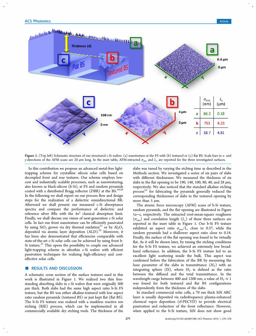
where n0, nH, and nL are the real part of the complex refractiveindex of the incident medium, high refractive index material,and low refractive index material, respectively. The firstomnidirectionality condition is presented in Figure 2. Giventhe refractive index of the incident medium, one can choose therefractive indexes of materials that will constitute the DBR insuch a way that their combination n0′ is greater than n0. Wedesigned our DBR around the band gap of c-Si with λB = 1000nm. Setting SiO2 as incident medium, a-Si:H (nH) and a-SiNx:H(nL) were considered good candidates for constituting ourdielectric DBR. Their refractive indexes at λB satisfied the firstomnidirectionality condition (n0′ = 1.58 > n0 = 1.5), and theirthickness in the DBR was determined as dH(L) = λB/4nH(L), withdH(L) the thickness of a-Si:H (a-SiNx:H).
28
Optical simulations of a flat stack of c-Si (half space)/SiO2(100 nm)/DBR, depicted in Figure 3a, were carried out. Theaim of these simulations was to find a minimum number of a-Si:H/a-SiNx:H pairs that results in Rb = 1 and fulfills the secondomnidirectionality condition. As Figure 3b shows, bothrequirements are met using six pairs of a-Si:H (69 nm)/a-SiNx:H (146 nm). This number of pairs represents a goodcompromise between processing time of the DBR and highinternal rear reflectance. In Figure 3b the theoretical angle-dependent Bragg wavelength (λB) and the right and leftphotonic band gap edges (λL and λR, respectively) are alsodepicted. It is noticeable that the results of our optical modelingusing materials with wavelength-dependent properties wereclose to the theory.28 The typical quenching of λR in P-polarization due to the Brewster angle was reproduced as well.These optical simulations rigorously describe the internal rearreflectance in our ultrathin c-Si slabs coated with dielectric DBRat the flat BS. On the other hand, considering the textured BS,we expect some deviation in the internal rear reflectance, as thesimulated thicknesses can be realized in practice only on a flatsurface. A cross-sectional scanning electron microscopy (SEM)image of the 20 μm thick textured and 28 μm flat c-Si slabs withdielectric omnidirectional DBR are shown in Figure 4a and b,respectively. The b-Si FS texture (green inset) is the same forboth BS configurations. Random pyramidal BS textureconformally coated by the designed DBR is clearly visible onthe 20 μm thick bulk c-Si (red inset in Figure 4a). Analyzingthese images, we found that the morphology of b-Si texture ischaracterized by conical shapes having a radius around 250 nmand a height lower than 1 μm. These values are in reasonableagreement with the results obtained from the AFM technique.All fabricated slabs in both BS configurations and with
different BRs were optically characterized by measuring thereflectance and transmittance (R and T) in the wavelength
Figure 2. Contour plot depicting the first omnidirectionalitycondition: n0′ > n0 (eq 1). Light blue lines on the contour plot arethe isovalue curves indicating the refractive index of the incidentmedium (n0) on top of the DBR. To fulfill this condition for a DBR(n0′ = f(nL,nH)) having bulk c-Si as incident medium (n0) (see yellowarea), nonabsorbing materials with high nL and nH refractive indexes atλB = 1000 nm are required. Their fabrication is however not trivial.Instead, considering a SiO2 layer (n0 = nSiO2(1000 nm) = 1.5) between thebulk c-Si and DBR allows for the use of existing nonabsorbingmaterials, λB = 1000 nm, such as a-SiNx:H (nL = na‑SiNx(1000 nm) = 1.76,da‑SiNx = 146 nm) and a-Si:H (nH = na‑Si:H(1000 nm) = 3.61, da‑Si:H = 69nm).
ACS Photonics Article
dx.doi.org/10.1021/ph4001586 | ACS Photonics 2014, 1, 270−278272

range between 400 and 1200 nm using the IS. Totalabsorptance (Atot) was calculated as Atot = 1 − R − T. Thisquantity corresponds to the absorptance in silicon (Asi) onlywhen the BR is constituted by nonabsorbing materials. On theother hand, in case of metallic BR the measured Atot includesalso the absorption in the metal layer. To compare only Asi forboth BR configurations, we used our analytical model that iscapable of distinguishing Asi from Atot
32 (see Methods section,eq 4). The experimentally determined ASi were thereforecompared with absorptances calculated from the 4n2 classicalabsorption limit (A4n2) and the single pass limit (ASP):
10
α= −
+A
d1
11 4nn4
Si2
Si
2
(2)
= − α−A 1 e dSP
Si (3)
where nSi and αSi are the real part of the complex refractiveindex and the absorption coefficient of c-Si, respectively.The measured Asi of a 20 μm (28 μm) thick c-Si slab in the
case of the b-Si FS texture and alkaline-textured (flat) BScoated with either dielectric DBR or reference Ag are reportedin Figure 5a and b, respectively. Considering both figures, it isclear that the absorptance in our nanotextured c-Si wafers forboth BRs is much higher than that calculated according to thesingle pass limit. This highlights the goodness of the scatteringproperties of the developed nanotexturing. However, thetexturing of the BS with random pyramids introduces anadditional level of scattering, which eventually enhances theNIR response. Even though the front b-Si nanotexture achievesan excellent broad-band antireflective effect at the air/siliconfront interface, we speculate that it may not actuate aLambertian scattering inside the c-Si absorbers. In this respect,we recognize that further work has to be done from the
Figure 3. (a) Simulated structure and (b) calculated internal reflectance for different angles of incidence and for P-polarization (left) and S-polarization (right). The gray shaded area represents the omnidirectional photonic band gap (second omnidirectional condition). The whitehorizontal solid and dashed curves are the theoretical angle-dependent photonic band edges (λL and λR) and the Bragg wavelength, respectively. Forangle of incidence 0°, λB is equal to 1000 nm. λL and λR, theoretically calculated
28 for wavelength-independent nL = 1.76 and nH = 3.61, closely followthe region of high reflectance in both polarizations. In the P-polarization panel, the vertical dash-dotted line locates the Brewster angle of the opticalsystem. The colors from violet to red represent the increasing value of the rear internal reflectance Rb for both polarizations.
Figure 4. Cross-sectional SEM images of (a) 20 μm thick absorber with textured BS and (b) 28 μm thick absorber with flat BS. The three coloredinsets show a close-up of the common front nanotexture coated with thermal SiO2 (green) and of the textured (red) and the flat (blue) BS coatedwith thermal SiO2 and six pairs of a-Si:H/a-SiNx:H conformal DBR. All SEM images were taken at a tilt angle of 45°.
ACS Photonics Article
dx.doi.org/10.1021/ph4001586 | ACS Photonics 2014, 1, 270−278273

perspective of angular intensity distribution33 obtained by frontb-Si nanotexture inside the c-Si absorbers.Integrating the measured absorptance spectra of all our
structured absorber slabs with the reference solar photon flux inthe wavelength range between 400 and 1200 nm (see Methodssection, eq 7), we could calculate the so-called implied JPH.Considering the thickness of the realized slabs and operatingthe same calculation in the identical wavelength range but usingeither A4n2 or ASP, we could also carry out the implied JPH of the4n2 classical absorption limit and of the single pass limit. Inparticular, in the case of a 20 μm thick c-Si slab with texturedBS, we achieved 99% and 99.8% of the implied JPH of thetheoretical 4n2 classical absorption limit with dielectric andmetallic BR, respectively. To our knowledge, this is so far theclosest experimental evidence of the 4n2 classical absorptionlimit.In Figure 5b the simulated internal reflectance for the flat BS
coated with DBR is also reported. The designed wavelengthrange of high internal reflectance of the DBR (800−1200 nm)perfectly matches the weak-absorption region of c-Si. However,in the case of even thinner wafers, the limited bandwidth of theDBR would lead to a decrease of the optical absorption alreadyin the red response. To overcome such a limitation, amodulated DBR can be used to achieve broader bandwidth.28,34
The slab with the dielectric DBR on flat BS shows slightlyhigher absorptance compared with the reference Ag BR. Theopposite outcome is observed in the case of our record slabwith textured BS. To explain this behavior, we looked at thespectral losses of the two BRs in both BS configurations andcalculated their implied JPH. The spectral losses are due to thecalculated optical absorption in the metallic layer (Ag BR) orthe measured transmittance through the dielectric stack (DBR
BR). The DBR is optimized for flat interfaces, and therefore itshows slightly lower optical losses than Ag BR in the case of flatBS as presented in Figure 5d. Instead, in the case of textured BS(see Figure 5c), our DBR design suffers from higher opticallosses with respect to Ag BR, not being optimized for texturedinterfaces. This setback was found to be independent from theabsorber thickness, as depicted in Figure 6a,b.On the other hand, still looking at Figure 6a,b, what was
found to be thickness dependent was the gap between the JPH
Figure 5. Measured absorptances in the case of the b-Si FS texture and (a) 20 μm thick c-Si absorber with the alkaline textured BS or (b) 28 μmthick c-Si absorber with the flat BS. In both figures the absorptances of silicon with the optimized dielectric DBR and the reference 100 nm thick Aglayer BRs are reported. Absorptances are compared with the 4n2 classical absorption limit and single pass absorption (green and pink curves,respectively). Black line in (b) shows the simulated internal rear reflectance in c-Si with the optimized DBR. This spectrum corresponds toperpendicular incidence (0°) and was extracted from Figure 3. Panels (c) and (d) show the optical losses related to the Ag absorptance (calculated)in the case of metallic BR and transmittance (measured) in the case of dielectric DBR for textured and flat BS, respectively. The impliedphotocurrent densities of such optical losses were calculated according to eq 5 of the Methods section, using AAg (calculated) or TDBR (measured) inplace of ASi.
Figure 6. JPH calculated between 400 and 1200 nm for AM1.5illumination conditions and different absorber thicknesses in the caseof (a) textured and (b) flat BS (see eq 5 in the Methods section). TheBS is coated either with DBR or with the reference Ag BR.
ACS Photonics Article
dx.doi.org/10.1021/ph4001586 | ACS Photonics 2014, 1, 270−278274

predicted by the 4n2 limit and the one calculated from themeasured absorptances. In the case of textured BS, such a gapclearly decreases for thinner absorbers endowed with both BRs.Instead, in the case of flat BS, such a trend is less evident, as thegap for both BRs decreases at a slower pace. Either way, in oursamples with textured BS the gap reduced to 1% or less forabsorber thicknesses smaller than 35 μm. This thickness seemsbe a threshold below which the additional scattering effectintroduced by the rear random pyramids eventually starts tosupport the nonideal Lambertian scattering in the c-Si absorbergiven by the front nanotexture. The fact that the gapmonotonically decreases for smaller absorber thicknessescould be related to an enhanced photon absorption at longwavelengths due to a better coupling of the electromagneticfield with diffraction modes introduced by the back sidescattering, as illustrated in recent simulation results.35,36
The implied JPH determined for a double-sided texturedwafer coated with Ag BR with thicknesses equal to or less than35 μm approached the JPH predicted by the 4n2 limit asreported in Figure 6a. We believe that a similar result can beachieved on thin c-Si wafers with a DBR optimized for texturedBS. Therefore, further simulations studies are required to findthe optimum DBR design on textured BS that can outperformthe metallic BR. Considering the implied JPH based on theabsorptance spectra of 100 μm and 135 μm thick absorbers, wedid not approach the 4n2 absorption limit. However it isnoticeable that we obtained at least a 1 mA/cm2 higher JPHvalue with respect to state-of-the-art c-Si solar cells havingcomparable bulk thickness.37−40
Finally, we want to discuss the embedding of our light-trapping scheme in next-generation c-Si solar devices. Figure 7a
shows the 20 μm thick c-Si absorber slab extracted from the c-Si wafer support. Such a slab is flexible and can be processed tofabricate an ultrathin solar cell. Although our process flowinvolved a photolithographic step (see Methods section),mostly required for mechanical support and quality controlover pairs of slabs, our light-trapping scheme may bestraightforwardly implemented at an industrial level withmaskless processes. In our vision, the solar cell technologythat would take the highest efficiency gain from our light-trapping scheme is the one adopted by Sunpower,41,42 assketched in Figure 7b. The main feature of such a technology isthe fabrication of both contacts at the BS of the device. Thesecontacts are usually arranged in an interdigitated fashion, the
so-called interdigitated back contacted design (IBC). With thistype of solar cell technology, since no metal−Si contact isrequired at the FS (i.e., no metal front grid) and a lightly dopedfloating front emitter is usually employed,43 both low frontsurface recombination and parasitic emitter absorption in theblue region can be expected. For these reasons, the excellentbroad-band antireflective effect provided by our front nano-texturing could be fully exploited on the entire solar device area.It is clear that state-of-the-art passivation of FS of our c-Siultrathin absorbers must be preliminarily actuated in order tofabricate the solar device sketched in Figure 7b. In a futurepublication we shall present our improved passivation of b-Sinanotexturing using SiO2 and Al2O3 with a surface treatmentafter RIE aiming to increase minority carrier lifetime.21
■ CONCLUSIONS
We presented an advanced light-trapping scheme based on b-SiFS texture, random pyramid BS texture, and dielectric DBR.After designing a dielectric omnidirectional DBR for flat BR, werealized ultrathin textured c-Si slabs having thicknesses in therange between 190 and 20 μm. We measured c-Si absorptancespectra that, integrated between 400 and 1200 nm with thereference solar photon flux, resulted in implied JPH up to 99.8%of the maximal theoretical one calculated for the samewavelength range and wafer thickness. To our knowledge thisis the closest experimental evidence of the 4n2 classicalabsorption limit in c-Si. Further studies should aim at thefabrication of an optimized dielectric DBR that suffers less fromtransmittance losses in the region of weak absorption of c-Siwhen deposited on a textured surface. Additionally, the angledependence of light scattering given by the front nanotextureinside the c-Si absorber should be addressed. This is to pursuean even better antireflective front texture, which allows animplied JPH near the 4n2 absorption limit with flat BS. Webelieve that high-efficiency, ultrathin solar cells can befabricated once that the presented light-trapping scheme iswell passivated electrically. This can be achieved by combininga SiO2- or Al2O3-based passivation with a surface treatmentafter RIE, aiming to increase minority carrier lifetime.21 Finally,the IBC approach was indicated as the most suited technologyin order to fully exploit the optical advantages brought by ourlight-trapping scheme.
■ METHODS
Process Flow Description. We used 4 in. CZ p-type Siwafers with initial thickness 300 ± 5 μm and resistivity >1000Ω·cm. The front b-Si texture was made by RIE using a gaseousmixture of SF6 and O2 (see Figure 1a). This texturing processcan be realized also on n-type Si wafers. After standard cleaning,rinsing, and drying of the substrates, SiN was deposited on bothsides of the wafers in a tube furnace by means of low-pressurechemical vapor deposition (LP-CVD). On the nontextured sideof the wafers, a photolithographic step was performed to createtwo openings, each measuring 3 × 3 cm2 in area. In suchopenings the SiN layer was dry-etched in a C2F6 plasma for 20s. After that the photoresist outside the openings was dry-etched in a O2 plasma for 5 min (Europlasma stripper), and thesilicon bulk in the two openings was thinned in a bath of KOHat 80 °C characterized by an etching rate of 100 μm/h. Tuningthe etching time, we could fabricate two c-Si slabs in each of thesix different c-Si wafers. We measured the thickness of the slabsby means of a Veeco Dektak 150 profilometer, obtaining in
Figure 7. (a) Photo of 20 μm thick flexible silicon absorber extractedfrom the c-Si wafer support. Top-right and bottom-left photos indicatethe b-Si front surface and the rear random pyramids coated with DBR,respectively. (b) Our vision: to apply the presented light-trappingscheme in IBC c-Si solar cell technology.
ACS Photonics Article
dx.doi.org/10.1021/ph4001586 | ACS Photonics 2014, 1, 270−278275

each pair of openings 190, 135, 100, 80, 40, and 28 μm thickbulk c-Si, respectively. For each wafer, one of the openings wasfurther etched in a TMAH-IPA alkaline bath to get a texturecharacterized by random pyramids (textured BS, see Figure1b), while the other opening was kept flat by using AITechnology spin-coated thinning wax as a protective layerresistant to the alkaline solution (flat BS, see Figure 1c). Itshould be noted that TMAH-IPA texturing in the texturedopening reduces the Si thickness by more than 5 μm withrespect to the flat opening. The protective thinning wax layerwas later etched in acetone at room temperature for 2 min. Atthis point, the LP-CVD SiN, still present on the front of b-Siand on the rear side outside the openings, was etched from allsamples in a H3PO4 solution (85 wt % diluted in H2O) at 157°C for 42 min. A wet thermal SiO2 layer of 100 nm was grownon both sides of the wafers at 1100 °C in a tube furnace. To beable to compare the performance of the dielectric DBR withthat of a reference metallic BR using the same front/reartextured c-Si slabs, we first coated the rear side of the slabs witha 100 nm thick Ag layer (reference metallic BR) using physicalvapor deposition in a Provac PRO500S. After the opticalcharacterization of the samples (see the next section), weremoved the metallic BR in a HNO3 solution (69.5% diluted inH2O) at room temperature for 30 s, which left untouched c-Siand SiO2. Finally, the dielectric DBR was fabricated bydepositing six a-Si:H/a-SiNx:H pairs using SiH4 and SiH4 +NH3 plasmas in an rf-PECVD AMIGO Elettrorava cluster tool.Sample Characterization. The morphological analysis of
the samples was performed with AFM using an NT-MDTnTegra setup. Extracted values of σrms and LC are reported inthe inset table of Figure 1. For the visual investigation of thesurface textures, the thickness of c-Si textured slabs, and thecomposition of the DBR, a Philips XL-I50 SEM was used (seeFigure 4b). Wavelength-dependent complex refractive indexesof a-SiNx:H, a-Si:H, and SiO2 were extracted from ellipsometryspectra using a J. A. Wollam Co. M-2000DI spectroscopicellipsometer. At the design wavelength of our dielectric DBR(λB = 1000 nm), the real parts of the complex refractive indexesof a-SiNx:H, a-Si:H, and SiO2 were 1.76, 3.67, and 1.5,respectively. Reflectance (R) and transmittance (T) of
passivated FS/BS textured c-Si slabs with and without metallicBR or dielectric DBR were measured using an IS accessorymounted on a PerkinElmer Lambda 950 spectrophotometer inthe wavelength range between 400 and 1200 nm.
Optical Modeling and Implied PhotogeneratedCurrent Density. In an opaque optical system such as a c-Si/Ag stack, we developed an empirical model32 for which theabsorptance in silicon can be calculated as
=− − +
‐AR R R R
R
(1 )Si calc
air/Si @1200nm meas @1200nm
@1200nm
(4)
where Rmeas is the measured total reflectance, R@1200 nm isRmeas(1200 nm), and Rair/Si is the contribution of reflected lightbouncing inside the bulk c-Si at the air/Si interface, estimatedby linearly extrapolating Rmeas between 700−900 and 1200 nm.Measuring the total reflectance of an opaque optical system(i.e., no transmittance) such as c-Si/Ag means identifying alsothe total absorptance (Atot), which is given by the sum of theabsorptance spectra of c-Si (ASi) and Ag (AAg):
= + = − ⇒ = − −A A A R A R A1 1tot Si Ag meas Ag meas Si
(5)
Thus, using only Rmeas and eq 4, it is possible to distinguishfor this type of optical system ASi from AAg. To verify eq 4, weapply a three-step procedure. Even though we tested ourempirical model in several opaque optical systems and fordifferent absorber thicknesses, the validation of this model isreported here for the optical system c-Si (280 μm)/Ag (100nm) in both flat and pyramidally textured configurations. In thefirst step, we match measured Rmeas and Atot with thecorresponding Rsim and Atot‑sim using the optoelectricalsimulator Advanced Semiconductor Analysis (ASA) soft-ware.32,44,45 By achieving this goal, the software provides theabsorptance spectra in c-Si (ASi‑sim) and in Ag (AAg‑sim) suchthat Atot‑sim = ASi‑sim + AAg‑sim. In the second step, we calculatethe absorptance spectrum in c-Si (ASi‑calc) according to eq 4,and we compare this calculated spectrum with ASi‑sim. After thatwe calculate the absorptance spectrum in Ag (AAg‑calc) from
Figure 8. (a−c) Rmeas, Rair/Si, and Rsim for a 280 μm thick wafer coated on one side with 100 nm thick Ag back reflector in (a) flat and (c) pyramidallytextured configurations. The fabricated/simulated structures are sketched in the insets. (b−d) ASi‑cal and AAg‑cal calculated from eqs 4 and 6,respectively, and superposed to simulated ASi‑sim and AAg‑sim for the respective structures illustrated in the top insets. Also Atot and Atot‑sim spectra arehere reported. For both structures, the energy conservation (Rmeas + Atot = Rsim + Atot‑sim = Rmeas + Atot‑calc = 1) is verified (orange line).
ACS Photonics Article
dx.doi.org/10.1021/ph4001586 | ACS Photonics 2014, 1, 270−278276

= − −‐ ‐A R A1Ag calc meas Si calc (6)
Finally, in the third step, we sum up Rmeas, ASi‑calc, and AAg‑calc(i.e., Rmeas + Atot‑calc) aiming to observe 1 ∀λ, as it would be inthe case of Rmeas + Atot (see Figure 8).The implied photocurrent density (JPH) of absorptance in
textured c-Si slabs was calculated as follows:
∫ λ λ λ= − Φλ
λJ q A ( ) ( ) dPH Si AM1.5
1
2
(7)
where q is the elementary charge, ASi is the absorptance ofsilicon, ΦAM 1.5 is the standard AM1.5 photon flux,46 and [λ1, λ2]is the wavelength range of interest.
■ AUTHOR INFORMATIONCorresponding Author*E-mail: [email protected], [email protected], [email protected]. Fax: +31 15 27 82968.
Author ContributionsA.I. conceived the light-trapping scheme, conducted theexperiments and the measurements, wrote the manuscript,and composed the graphical material. A.I. and O.I. designed thedielectric DBR. O.I. carried out the optical simulations andadded supporting graphical material. O.I. and M.Z. supervisedthe work and proofread the manuscript.
NotesThe authors declare no competing financial interest.
■ ACKNOWLEDGMENTSThe authors thank M. Tijssen (TU Delft) for help with thedeposition of dielectric DBR, R. A. Vasudevan (TU Delft) forsupport with extraction of optical properties from ellipsometryspectra, Fai Tong Si and Dimitris Deligiannis for preparingsamples used in the Methods section, Delft Institute ofMicrosystems and Nanoelectronics (DIMES, TUDelft) forfacility services, and Dr. A. Poruba (SolarTec) for usefuldiscussions. This work was carried out with a subsidy from theDutch Ministry of Economic Affairs under the EOS-LTprogram (Project No. EOSLT10037).
■ REFERENCES(1) Zhao, J.; Wang, A.; Altermatt, P.; Green, M. A. 24% efficientsilicon solar cells with double layer antireflection coatings and reducedresistance loss. Appl. Phys. Lett. 1995, 66, 3636−3638.(2) Jager-Waldau, A. PV Status Report 2012; Joint Research Centre,Institute for Energy and Transport, 2012.(3) del Canizo, C.; del Coso, G.; Sinke, W. C. Crystalline silicon solarmodule technology: towards the 1 € per watt-peak goal. Prog. PhotovoltRes. Appl. 2008, 17, 199−209.(4) Goodrich, A.; Hacke, P.; Wang, Q.; Sopori, B.; Margolis, R.;James, T. L.; Woodhouse, M. A wafer-based monocrystalline siliconphotovoltaics road map: utilizing known technology improvementopportunities for further reductions in manufacturing costs. Sol. EnergyMater. Sol. 2013, 114, 110−135.(5) Micciche, B.; Dingle, B. Understanding the causes for cellbreakage during the cell interconnecting process−part I. Proceedings ofthe 21st European Photovoltaic Solar Energy Conference; 2006.(6) Munzer, K. A.; Holdermann, K. T.; Schlosser, R. E.; Sterk, S.Thin monocrystalline silicon solar cells. IEEE Trans. Electron Devices1999, 46, 2055−2061.(7) Glunz, S. W.; Rein, S.; Warta, W.; Knobloch, J.; Wettling, W. Onthe degradation of Cz-silicon solar cells. Proceedings of the 2nd WorldConference on Photovoltaic Energy Conversion; 1998; pp 1343−1346.
(8) Kray, D.; Kampwerth, H.; Schneiderlochner, E. Comprehensiveexperimental study on the performance of very thin laser-fired high-efficiency solar cells. Proceedings of the 19th European Photovoltaic SolarEnergy Conference; 2004; pp 608−611.(9) Green, M. A. Silicon Solar Cells: Advanced Principles & Practice;Centre for Photovoltaic Devices and Systems, University of NewSouth Wales, 1995.(10) Tiedje, T.; Yablonovitch, E.; Cody, G. D.; Brooks, B. G.Limiting efficiency of silicon solar cells. IEEE Trans. Electron Devices1984, 31, 711−716.(11) Campbell, P.; Green, M. A. Light trapping properties ofpyramidally textured surfaces. J. Appl. Phys. 1987, 62, 243.(12) Holman, Z. C.; Filipic, M.; Lipovsek, B.; De Wolf, S.; Smole, F.;Topic, M.; Ballif, C. Parasitic absorption in the rear reflector of asilicon solar cell: simulation and measurement of the sub-bandgapreflectance for common dielectric/metal reflectors. Sol. Energy Mater.Sol. 2014, 120, 426−430.(13) Wang, K. X.; Yu, Z.; Liu, V.; Cui, Y.; Fan, S. Absorptionenhancement in ultrathin crystalline silicon solar cells withantireflection and light-trapping nanocone gratings. Nano Lett. 2012,12, 1616−1619.(14) Garnett, E.; Yang, P. Light trapping in silicon nanowire solarcells. Nano Lett. 2010, 10, 1082−1087.(15) Cao, L.; Fan, P.; Vasudev, A. P.; White, J. S.; Yu, Z.; Cai, W.;Schuller, J. A.; Fan, S.; Brongersma, M. Semiconductor nanowireoptical antenna solar absorbers. Nano Lett. 2010, 10, 439−445.(16) Battaglia, C.; Boccard, M.; Haug, F.-J.; Ballif, C. Light trappingin solar cells: when does a Lambertian scatterer scatter Lambertianly?J. Appl. Phys. 2012, 112, 094504.(17) Isabella, O.; Ingenito, A.; Linssen, D.; Zeman M. Front/reardecoupled texturing in refractive and diffractive regimes for ultra-thinsilicon-based solar cells. Renewable Energy and the Environment, OSATechnical Digest; 2013, paper PM4C.2.(18) Wang, S.; Weil, B.; Li, Y.; Wang, K. X.; Garnett, E.; Fan, S.; Cui,Y. Large Area Free-Standing Ultrathin Single-Crystal Silicon asProcessable Materials. Nano Lett. 2013, 13, 4393−4398.(19) Zeng, L.; Yi, Y.; Hong, C.; Liu, J.; Feng, N.; Duan, X.; Kimerling,L. C.; Alamariu, B. A. Efficiency enhancement in Si solar cells bytextured photonic crystal BR. Appl. Phys. Lett. 2006, 89, 111111.(20) Isabella, O.; Dobrovolskiy, S.; Kroon, G. A.; Zeman, M. Designand application of dielectric distributed Bragg back reflector in thin-film silicon solar cells. J. Non-Cryst. Solids 2012, 358, 2295−2298.(21) Oh, J.; Yuan, H. C.; Branz, H. M. An 18.2%-efficient black-silicon solar cell achieved through control of carrier recombination innanostructures. Nat. Nanotechnol. 2012, 7, 743−748.(22) Otto, M.; Kroll, M.; Kasebier, T.; Salzer, R.; Tunnermann, A.;Wehrspohn, R. B. Extremely low surface recombination velocities inblack silicon passivated by atomic layer deposition. Appl. Phys. Lett.2012, 100, 191603.(23) Papet, P.; Nichiporuk, O.; Kaminski, A.; Rozier, Y.; Kraiem, J.;Lelievre, J.-F.; Chaumartin, A.; Fave, A.; Lemiti, M. Pyramidaltexturing of silicon solar cell with TMAH chemical anisotropicetching. Sol. Energy Mater. Sol. 2006, 90, 2319−2328.(24) Kroll, M.; Otto, M.; Kasebier, T.; Fuchsel, K.; Wehrspohn, R.;Kley, E.; Tunnermann, A.; Pertsch, T. Black silicon for solar cellapplications. Proc. SPIE 8438, Photonics Solar Energy Syst. IV 2012,843817.(25) Hoex, B.; Heil, S. B. S.; Langereis, E.; van de Sanden, M. C. M.;Kessels, W. M. M. Ultralow surface recombination of c-Si substratespassivated by plasma-assisted atomic layer deposited Al2O3. Appl. Phys.Lett. 2006, 89, 042112.(26) White papers in Ansys HFSS official website, http://www.ansoft.com/products/hf/hfss/.(27) Kray, D.; Hermle, M.; Glunz, S. W. Theory and experiments onthe back side reflectance of silicon wafer solar cells. Prog. Photovolt:Res. Appl. 2007, 16, 1−15.(28) Isabella, O. Light management in thin-film silicon solar cells.Ph.D. dissertation, 2013.
ACS Photonics Article
dx.doi.org/10.1021/ph4001586 | ACS Photonics 2014, 1, 270−278277

(29) Fink, Y.; Winn, J. N.; Fan, S.; Chen, C.; Michel, J.;Joannopoulos, J. D.; Thomas, E. L. A dielectric omnidirectionalreflector. Science 1998, 282 (5394), 1679−1682.(30) Chigrin, D. N.; Lavrinenko, A. V.; Yarotsky, D. A.; Gaponenko,S. V. Observation of total omnidirectional reflection from a one-dimensional dielectric lattice. Appl. Phys. 1999, 68, 25−28.(31) Orfanidis, J. S. Electromagnetic Waves and Antennas; RutgersUniversity, 2010.(32) Ingenito, A.; Isabella, O.; Zeman, M. Opto-electronic evaluationof thin double-textured crystalline silicon wafers. 39th IEEE Photo-voltaic Specialist Conference; 2013.(33) Jager, K.; Isabella, O.; van Swaaij, R. A. C. M. M.; Zeman, M.Angular resolved scattering measurements of nano-textured substratesin a broad wavelength range, Meas. Sci. Technol. 2010, 22, 10.1088/0957-0233/22/10/105601.(34) Krc, J.; Zeman, M.; Luxembourg, S. L.; Topic, M. Modulatedphotonic-crystal structures as broadband back reflectors in thin-filmsolar cells, Appl. Phys. Lett. 2009, 94, 10.1063/1.3109781.(35) Bermel, P.; Luo, C.; Zeng, L.; Kimerling, L.; Joannopoulos, J.Improving thin-film crystalline silicon solar cell efficiencies withphotonic crystals. Opt. Express 2007, 15, 16986−17000.(36) Biswas, R.; Xu, C. Nano-crystalline silicon solar cell architecturewith absorption at the classical 4n2 limit. Opt. Express 2011, 19, A664−A672.(37) Kinoshita, T.; Fujishima, D.; Yano, A.; Ogane, A.; Tohoda, S.;Matsuyama, K.; Nakamura, Y.; Tokuoka, N.; Kanno, H.; Sakata, H.;Taguchi, M.; Maruyama, E. The approaches for high efficiency HITsolar cell with very thin (<100mm) silicon wafer over 23%. Proceedingsof the 26th European Photovoltaic Solar Energy Conference; 2011;Hamburg, Germany.(38) Cousins, P. J.; Smith, D. D.; Luan, H.-C.; Manning, J.; Dennis,T. D.; Waldhauer, A.; Wilson, K. E.; Harley, G.; Mulligan, W. P.Generation 3: improved performance at lower cost. Proceedings of the35th Photovoltaic Specialists Conference; 2010; pp 275−278.(39) Swanson, D. Solar Energy Mini-Series: The Silicon PhotovoltaicRoadmap; Stanford University, 2011, http://energyseminar.stanford.edu/sites/all/files/eventpdf/11-11-14%20Swanson.pdf.(40) Green, M. A.; Emery, K.; Hishikawa, Y.; Warta, W.; Dunlop, E.D. Solar cell efficiency tables (version 41). Prog. Photovolt: Res. Appl.2013, 21.(41) Swanson, R. M. Device physics for backside-contact solar cells.Proceedings of the 33rd IEEE Photovoltaic Specialists Conference; SanDiego, CA, USA, 2008.(42) http://us.sunpowercorp.com/homes/.(43) Ohrdes, T.; Romer, U.; Larionova, Y.; Peibst, R.; Altermatt, P.P.; Harder, N.-P. High fill-factors of back-junction solar cells withoutfront surface field diffusion. Proceedings of the 27th EuropeanPhotovoltaic Solar Energy Conference; 2012; pp 866−869(44) Isabella, O.; Sai, H.; Kondo, M.; Zeman, M. Full-waveoptoelectrical modeling of optimized flattened light-scatteringsubstrate for high efficiency thin-film silicon solar cells. Prog. Photovolt:Res. Appl. 2012, DOI: 10.1002/pip.2314.(45) Zeman, M.; Isabella, O.; Solntsev, S.; Jager, K. Modelling ofthin-film silicon solar cells. Sol. Energ. Mat. Sol. 2013, DOI: 10.1016/j.solmat.2013.05.037.(46) http://rredc.nrel.gov/solar/spectra/am1.5/.
ACS Photonics Article
dx.doi.org/10.1021/ph4001586 | ACS Photonics 2014, 1, 270−278278