experiment number 2 schematic capture and logic simulation...
TRANSCRIPT
2-1
EXPERIMENT NUMBER 2
SCHEMATIC CAPTURE AND
LOGIC SIMULATION (EDA-1) Purpose
The purpose of this exercise is to familiarize you with two common electronic design automation (EDA) tools: schematic capture and logic simulation. Although hardware description languages (HDL) are being used in industry more and more, schematic capture is still the predominant design entry technique. We will be using the suite of EDA tools supplied by Altera Quartus-II software and
ModelSim-Altera. The general philosophy of CpE112 is to design a circuit, enter its schematic into a design database using Altera Quartus-II, simulate the design to verify that it is correct using ModelSim-Altera, and verify the actual hardware by using the design to program a field programmable gate array (FPGA). The object of this first EDA tutorial is to go through the basic process of schematic capture and logic simulation using an extremely simple circuit composed of some basic primitive gates.
References Tutorial: Introduction to Digital Design with Using Schematic Capture with Altera Quartus-
II and Simulation using ModelSim-Altera. Materials Required
Altera Quartus-II, ModelSim-Altera Preliminary
Read through the tutorial to familiarize yourself with the steps you will be performing. You may want to highlight these steps in your lab book before coming to lab. Write truth tables for the four primitive gates used in the tutorial. Find data sheets for the parts on the internet. Procedure
Work through the tutorial in the lab. Take notes as you are going through the procedures. You may want to refer back to your notes later when doing other labs. You might want to use a highlighter in this lab so you can find important parts quickly later on – I guarantee you’ll be turning back to this lab for directions in the future. There are questions scattered throughout the tutorial. You should answer these questions and submit them together with hardcopies of the schematic and simulation list output as a report along with any other material your TA might require.

2-2
Tutorial
Using Schematic Capture with Altera Quartus-II
Quartus II is a sophisticated CAD system. As most commercial CAD tools are continuously
being improved and updated, Quartus II has gone through a number of releases. The version known as Quartus II 8.0 is used in this tutorial. For simplicity, in our discussion we will refer to this software package simply as Quartus II.
In this tutorial we introduce the design of logic circuits using Quartus II. Step-by-step instructions are presented for performing design entry with two methods: using schematic capture and writing Verilog code, as well as with a combination of the two.
1. Introduction This tutorial assumes that the reader has access to a computer on which Quartus II is installed.
Instructions for installing Quartus II are provided with the software. The Quartus II software will run on several different types of computer systems. For this tutorial a computer running a Microsoft operating system (Windows NT, Windows 2000, or Windows XP) is assumed. Although Quartus II operates similarly on all of the supported types of computers, there are some minor differences. A reader who is not using a Microsoft Windows operating system may experience some slight discrepancies from this tutorial. Examples of potential differences are the locations of files in the computer’s file system and the exact appearance of windows displayed by the software. All such discrepancies are minor and will not affect the reader’s ability to follow the tutorial.
This tutorial does not describe how to use the operating system provided on the computer. We assume that the reader already knows how to perform actions such as running programs, operating a mouse, moving, resizing, minimizing and maximizing windows, creating directories (folders) and files, and the like. A reader who is not familiar with these procedures will need to learn how to use the computer’s operating system before proceeding.
1.1 Getting Started Each logic circuit, or subcircuit, being designed in Quartus II is called a project. The software
works on one project at a time and keeps all information for that project in a single directory in the file system (we use the traditional term directory for a location in the file system, but in Microsoft Windows the term folder is used). To begin a new logic circuit design, the first step is to create a directory to hold its files. We usually store the project in the S drive. Please create a folder named CpE112 in your S drive and a subfolder named lab2 inside it.
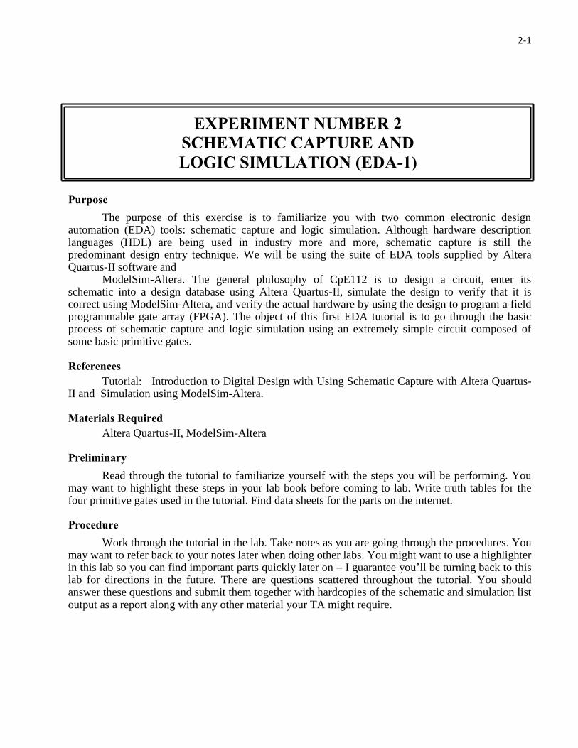
Start the Quartus II software. You should see a display similar to the one in Figure 1. This display consists of several windows that provide access to all features of Quartus II, which the user selects with the computer mouse.
2-3
Figure 1
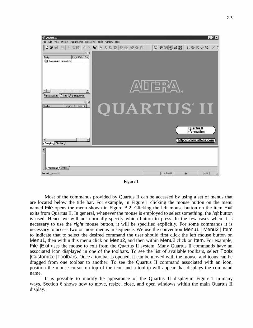
Most of the commands provided by Quartus II can be accessed by using a set of menus that
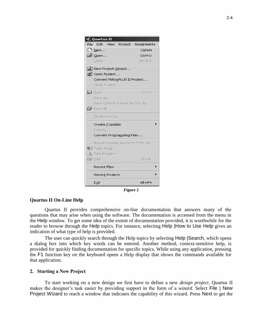
are located below the title bar. For example, in Figure.1 clicking the mouse button on the menu named File opens the menu shown in Figure B.2. Clicking the left mouse button on the item Exit exits from Quartus II. In general, whenever the mouse is employed to select something, the left button is used. Hence we will not normally specify which button to press. In the few cases when it is necessary to use the right mouse button, it will be specified explicitly. For some commands it is necessary to access two or more menus in sequence. We use the convention Menu1 | Menu2 | Item to indicate that to select the desired command the user should first click the left mouse button on Menu1, then within this menu click on Menu2, and then within Menu2 click on Item. For example, File |Exit uses the mouse to exit from the Quartus II system. Many Quartus II commands have an associated icon displayed in one of the toolbars. To see the list of available toolbars, select Tools |Customize |Toolbars. Once a toolbar is opened, it can be moved with the mouse, and icons can be dragged from one toolbar to another. To see the Quartus II command associated with an icon, position the mouse cursor on top of the icon and a tooltip will appear that displays the command name.
It is possible to modify the appearance of the Quartus II display in Figure 1 in many ways. Section 6 shows how to move, resize, close, and open windows within the main Quartus II display.
2-4
Figure 2
Quartus II On-Line Help
Quartus II provides comprehensive on-line documentation that answers many of the questions that may arise when using the software. The documentation is accessed from the menu in the Help window. To get some idea of the extent of documentation provided, it is worthwhile for the reader to browse through the Help topics. For instance, selecting Help |How to Use Help gives an indication of what type of help is provided.
The user can quickly search through the Help topics by selecting Help |Search, which opens a dialog box into which key words can be entered. Another method, context-sensitive help, is provided for quickly finding documentation for specific topics. While using any application, pressing the F1 function key on the keyboard opens a Help display that shows the commands available for that application.
2. Starting a New Project
To start working on a new design we first have to define a new design project. Quartus II makes the designer’s task easier by providing support in the form of a wizard. Select File | New Project Wizard to reach a window that indicates the capability of this wizard. Press Next to get the
2-5
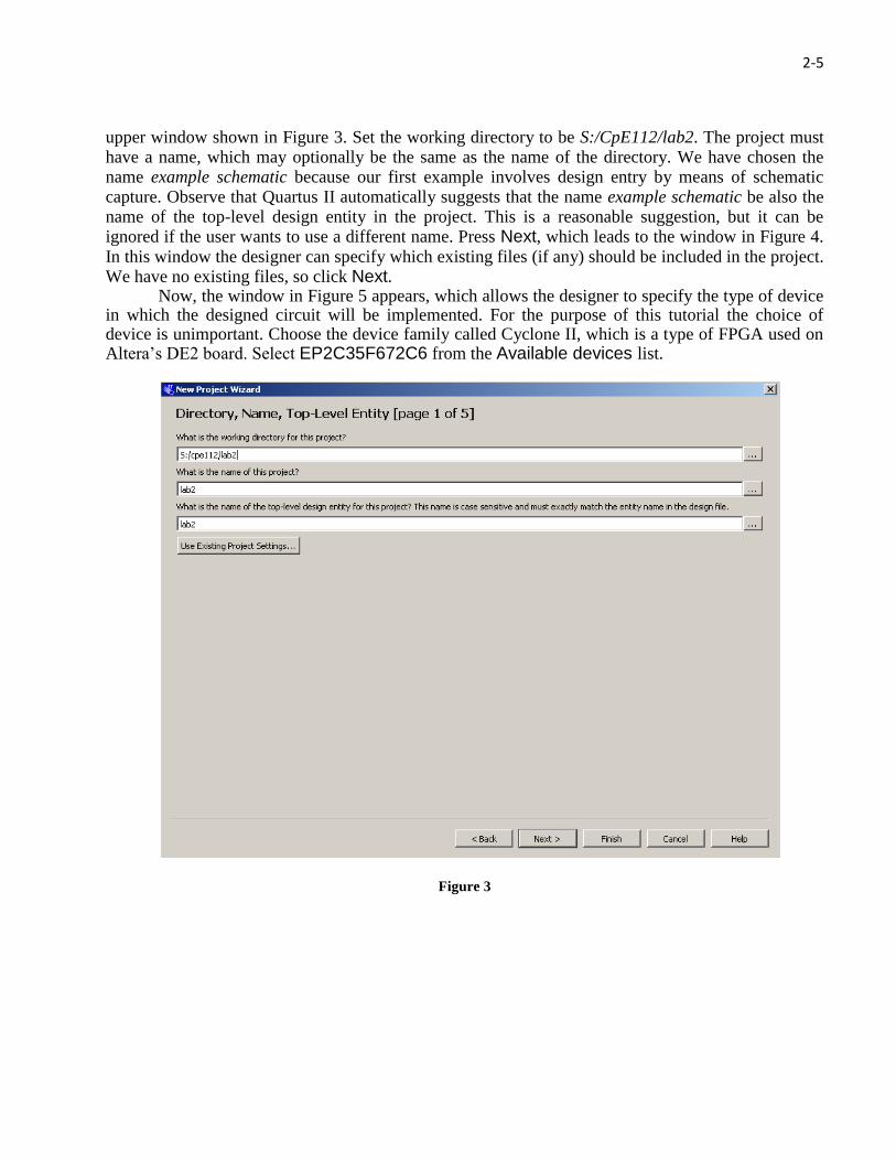
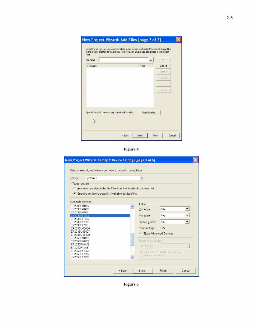
upper window shown in Figure 3. Set the working directory to be S:/CpE112/lab2. The project must have a name, which may optionally be the same as the name of the directory. We have chosen the name example schematic because our first example involves design entry by means of schematic capture. Observe that Quartus II automatically suggests that the name example schematic be also the name of the top-level design entity in the project. This is a reasonable suggestion, but it can be ignored if the user wants to use a different name. Press Next, which leads to the window in Figure 4.
In this window the designer can specify which existing files (if any) should be included in the project. We have no existing files, so click Next.
Now, the window in Figure 5 appears, which allows the designer to specify the type of device in which the designed circuit will be implemented. For the purpose of this tutorial the choice of device is unimportant. Choose the device family called Cyclone II, which is a type of FPGA used on Altera’s DE2 board. Select EP2C35F672C6 from the Available devices list.
Figure 3
2-6
Figure 4
Figure 5
2-7
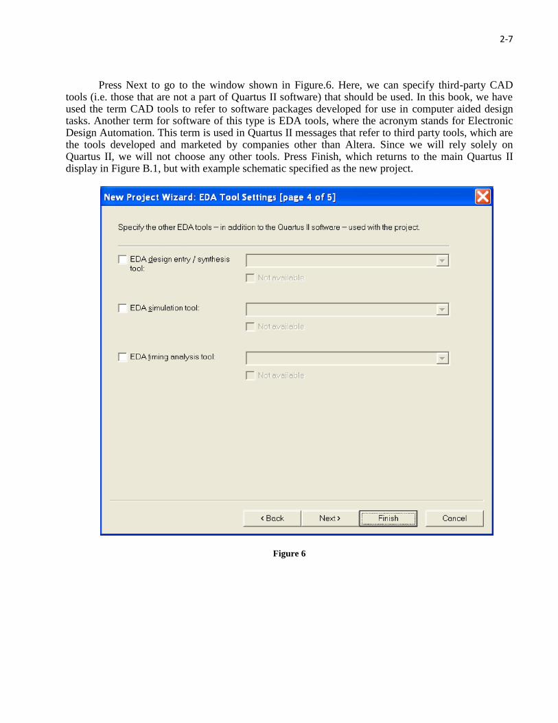
Press Next to go to the window shown in Figure.6. Here, we can specify third-party CAD tools (i.e. those that are not a part of Quartus II software) that should be used. In this book, we have used the term CAD tools to refer to software packages developed for use in computer aided design tasks. Another term for software of this type is EDA tools, where the acronym stands for Electronic Design Automation. This term is used in Quartus II messages that refer to third party tools, which are the tools developed and marketed by companies other than Altera. Since we will rely solely on Quartus II, we will not choose any other tools. Press Finish, which returns to the main Quartus II display in Figure B.1, but with example schematic specified as the new project.
Figure 6
2-8
3. Design Entry Using Schematic Capture
As explained in Chapter 2, commonly used design entry methods include schematic capture and Verilog code. This section illustrates the process of using the schematic capture tool provided in Quartus II, which is called the Block Editor. As a simple example, we will draw a schematic for the 4 logic function---and, nand, nor, or. After creating the schematic, we show how to use the modelsim to verify the correctness of the designed circuit.
3.1 Using the Block Editor
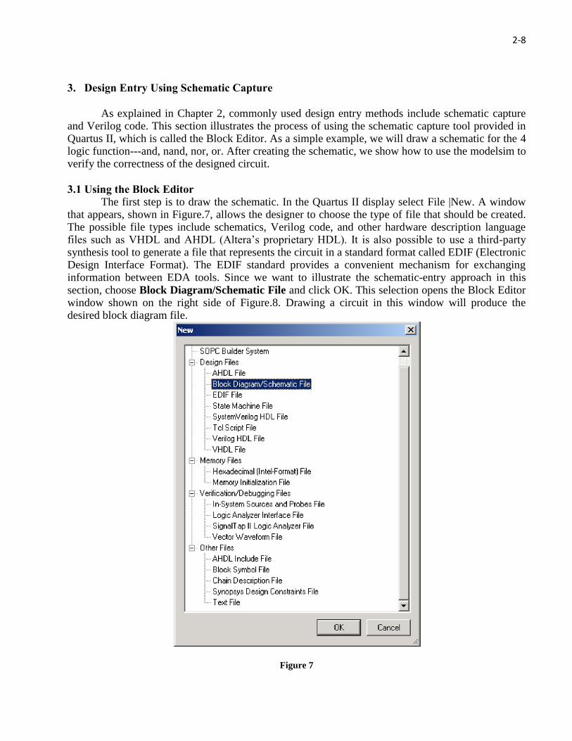
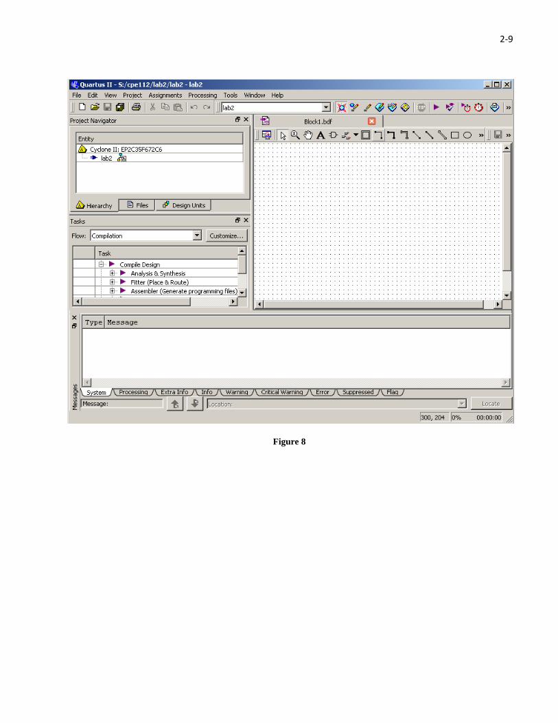
The first step is to draw the schematic. In the Quartus II display select File |New. A window that appears, shown in Figure.7, allows the designer to choose the type of file that should be created. The possible file types include schematics, Verilog code, and other hardware description language files such as VHDL and AHDL (Altera’s proprietary HDL). It is also possible to use a third-party synthesis tool to generate a file that represents the circuit in a standard format called EDIF (Electronic Design Interface Format). The EDIF standard provides a convenient mechanism for exchanging information between EDA tools. Since we want to illustrate the schematic-entry approach in this section, choose Block Diagram/Schematic File and click OK. This selection opens the Block Editor window shown on the right side of Figure.8. Drawing a circuit in this window will produce the desired block diagram file.
Figure 7
2-9
Figure 8
2-10
Importing Logic Gate Symbols
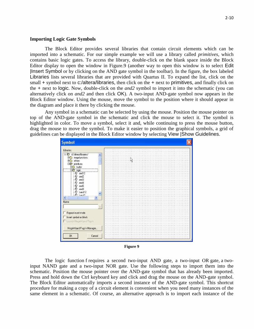
The Block Editor provides several libraries that contain circuit elements which can be imported into a schematic. For our simple example we will use a library called primitives, which contains basic logic gates. To access the library, double-click on the blank space inside the Block
Editor display to open the window in Figure.9 (another way to open this window is to select Edit |Insert Symbol or by clicking on the AND gate symbol in the toolbar). In the figure, the box labeled Libraries lists several libraries that are provided with Quartus II. To expand the list, click on the small + symbol next to c:/altera/libraries, then click on the + next to primitives, and finally click on the + next to logic. Now, double-click on the and2 symbol to import it into the schematic (you can alternatively click on and2 and then click OK). A two-input AND-gate symbol now appears in the Block Editor window. Using the mouse, move the symbol to the position where it should appear in the diagram and place it there by clicking the mouse.
Any symbol in a schematic can be selected by using the mouse. Position the mouse pointer on top of the AND-gate symbol in the schematic and click the mouse to select it. The symbol is highlighted in color. To move a symbol, select it and, while continuing to press the mouse button, drag the mouse to move the symbol. To make it easier to position the graphical symbols, a grid of guidelines can be displayed in the Block Editor window by selecting View |Show Guidelines.
Figure 9
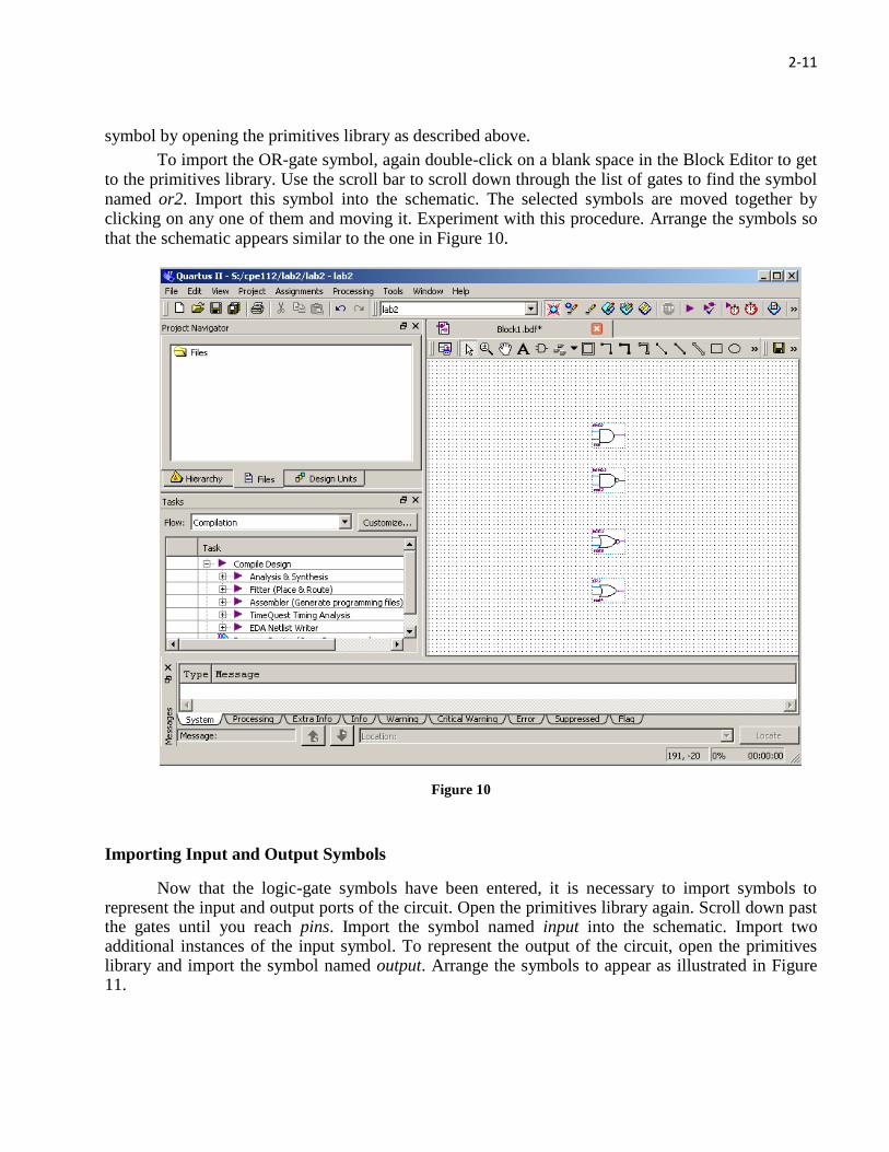
The logic function f requires a second two-input AND gate, a two-input OR gate, a two-
input NAND gate and a two-input NOR gate. Use the following steps to import them into the schematic. Position the mouse pointer over the AND-gate symbol that has already been imported. Press and hold down the Ctrl keyboard key and click and drag the mouse on the AND-gate symbol. The Block Editor automatically imports a second instance of the AND-gate symbol. This shortcut procedure for making a copy of a circuit element is convenient when you need many instances of the same element in a schematic. Of course, an alternative approach is to import each instance of the
2-11
symbol by opening the primitives library as described above. To import the OR-gate symbol, again double-click on a blank space in the Block Editor to get
to the primitives library. Use the scroll bar to scroll down through the list of gates to find the symbol named or2. Import this symbol into the schematic. The selected symbols are moved together by clicking on any one of them and moving it. Experiment with this procedure. Arrange the symbols so that the schematic appears similar to the one in Figure 10.
Figure 10
Importing Input and Output Symbols
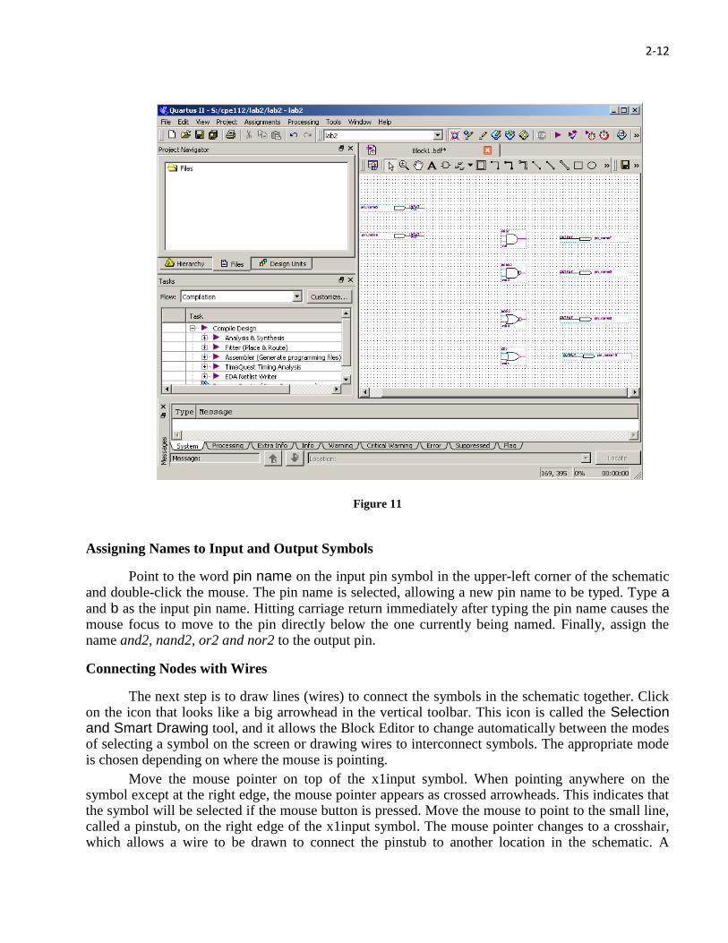
Now that the logic-gate symbols have been entered, it is necessary to import symbols to represent the input and output ports of the circuit. Open the primitives library again. Scroll down past the gates until you reach pins. Import the symbol named input into the schematic. Import two additional instances of the input symbol. To represent the output of the circuit, open the primitives library and import the symbol named output. Arrange the symbols to appear as illustrated in Figure 11.
2-12
Figure 11
Assigning Names to Input and Output Symbols
Point to the word pin name on the input pin symbol in the upper-left corner of the schematic and double-click the mouse. The pin name is selected, allowing a new pin name to be typed. Type a and b as the input pin name. Hitting carriage return immediately after typing the pin name causes the mouse focus to move to the pin directly below the one currently being named. Finally, assign the name and2, nand2, or2 and nor2 to the output pin. Connecting Nodes with Wires
The next step is to draw lines (wires) to connect the symbols in the schematic together. Click on the icon that looks like a big arrowhead in the vertical toolbar. This icon is called the Selection and Smart Drawing tool, and it allows the Block Editor to change automatically between the modes of selecting a symbol on the screen or drawing wires to interconnect symbols. The appropriate mode is chosen depending on where the mouse is pointing.
Move the mouse pointer on top of the x1input symbol. When pointing anywhere on the symbol except at the right edge, the mouse pointer appears as crossed arrowheads. This indicates that the symbol will be selected if the mouse button is pressed. Move the mouse to point to the small line, called a pinstub, on the right edge of the x1input symbol. The mouse pointer changes to a crosshair, which allows a wire to be drawn to connect the pinstub to another location in the schematic. A

2-13
connection between two or more pinstubs in a schematic is called a node. The name derives from electrical terminology, where the term node refers to any number of points in a circuit that are connected together by wires.
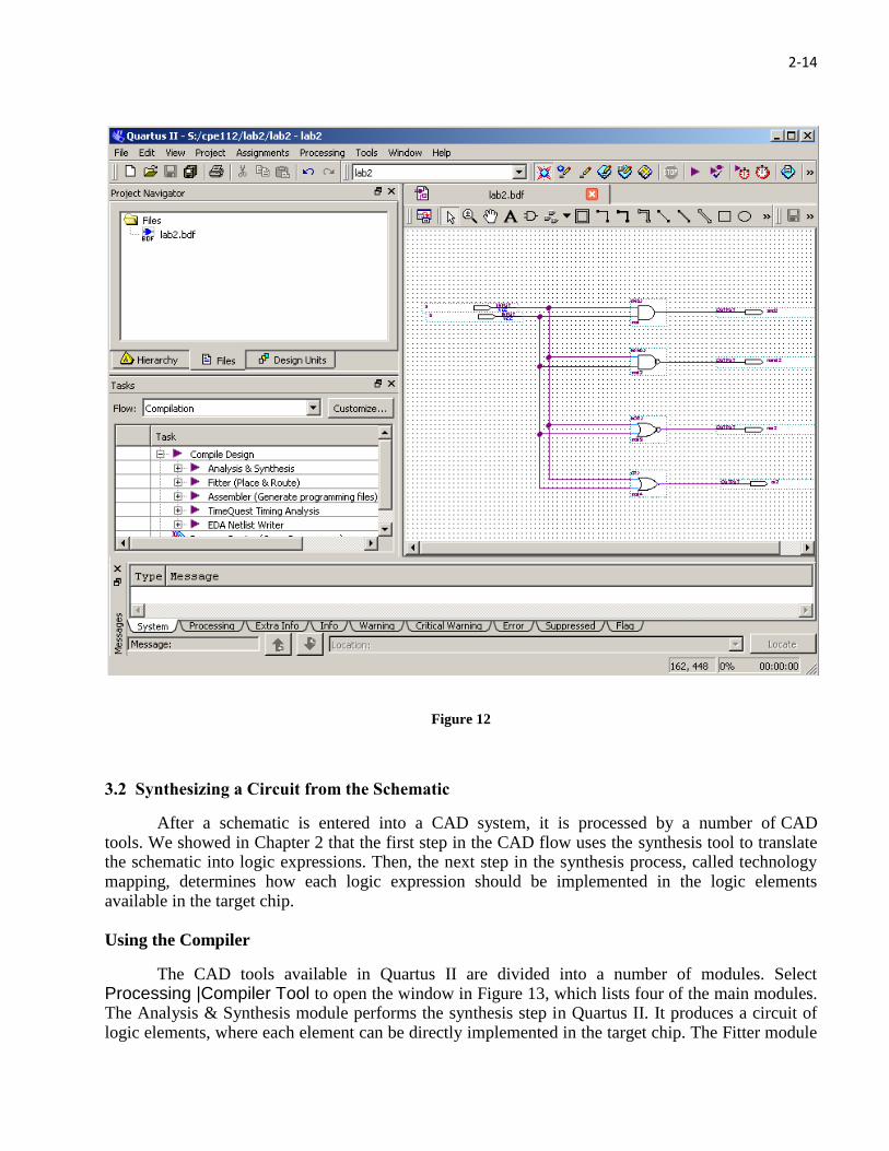
Connect the input symbol for x1to the AND gate at the top of the schematic as follows. While the mouse is pointing at the pinstub on the x1symbol, click and hold the mouse button. Drag the mouse to the right until the line (wire) that is drawn reaches the pinstub on the top input of the AND gate; then release the button. The two pinstubs are now connected and represent a single node in the circuit.
Use the same procedure to draw a wire from the pinstub on the x2 input symbol to the other input on the AND gate. Finally, the circuit appears as illustrated in Figure 12.
If any mistakes are made while connecting the symbols, erroneous wires can be selected with the mouse and then removed by pressing the Delete key or by selecting Edit |Delete. Save the schematic using File |Save As and choose the name example schematic. Note that the saved file is called example lab2.bdf.
Try to rearrange the layout of the circuit by selecting one of the gates and moving it. Observe that as you move the gate symbol all connecting wires are adjusted automatically. This takes place because Quartus II has a feature called rubberbanding which was activated by default when you chose to use the Selection and Smart Drawing tool. There is a rubberbanding icon, which is the icon in the toolbar that looks like an L-shaped wire with small tick marks on the corner. Observe that this icon is highlighted to indicate the use of rubberbanding. Turn the icon off and move one of the gates to see the effect of this feature.
Since our example schematic is quite simple, it is easy to draw all the wires in the circuit without producing a messy diagram. However, in larger schematics some nodes that have to be connected may be far apart, in which case it is awkward to draw wires between them. In such cases the nodes are connected by assigning labels to them, instead of drawing wires. See Help for a more detailed description.
2-14
Figure 12
3.2 Synthesizing a Circuit from the Schematic
After a schematic is entered into a CAD system, it is processed by a number of CAD tools. We showed in Chapter 2 that the first step in the CAD flow uses the synthesis tool to translate the schematic into logic expressions. Then, the next step in the synthesis process, called technology mapping, determines how each logic expression should be implemented in the logic elements available in the target chip.
Using the Compiler
The CAD tools available in Quartus II are divided into a number of modules. Select Processing |Compiler Tool to open the window in Figure 13, which lists four of the main modules. The Analysis & Synthesis module performs the synthesis step in Quartus II. It produces a circuit of logic elements, where each element can be directly implemented in the target chip. The Fitter module
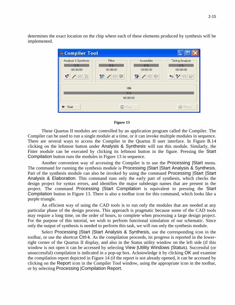
2-15
determines the exact location on the chip where each of these elements produced by synthesis will be implemented.
Figure 13
These Quartus II modules are controlled by an application program called the Compiler. The
Compiler can be used to run a single module at a time, or it can invoke multiple modules in sequence. There are several ways to access the Compiler in the Quartus II user interface. In Figure B.14 clicking on the leftmost button under Analysis & Synthesis will run this module. Similarly, the Fitter module can be executed by clicking its leftmost button in the figure. Pressing the Start Compilation button runs the modules in Figure 13 in sequence.
Another convenient way of accessing the Compiler is to use the Processing |Start menu. The command for running the synthesis module is Processing |Start |Start Analysis & Synthesis. Part of the synthesis module can also be invoked by using the command Processing |Start |Start Analysis & Elaboration. This command runs only the early part of synthesis, which checks the design project for syntax errors, and identifies the major subdesign names that are present in the project. The command Processing |Start Compilation is equivalent to pressing the Start Compilation button in Figure 13. There is also a toolbar icon for this command, which looks like a purple triangle.
An efficient way of using the CAD tools is to run only the modules that are needed at any particular phase of the design process. This approach is pragmatic because some of the CAD tools may require a long time, on the order of hours, to complete when processing a large design project. For the purpose of this tutorial, we wish to perform functional simulation of our schematic. Since only the output of synthesis is needed to perform this task, we will run only the synthesis module.
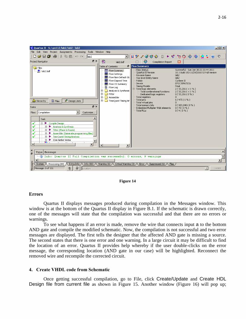
Select Processing |Start |Start Analysis & Synthesis, use the corresponding icon in the toolbar, or use the shortcut Ctrl-k. As the compilation proceeds, its progress is reported in the lower-right corner of the Quartus II display, and also in the Status utility window on the left side (if this window is not open it can be accessed by selecting View |Utility Windows |Status). Successful (or unsuccessful) compilation is indicated in a pop-up box. Acknowledge it by clicking OK and examine the compilation report depicted in Figure 14 (if the report is not already opened, it can be accessed by clicking on the Report icon in the Compiler Tool window, using the appropriate icon in the toolbar, or by selecting Processing |Compilation Report.
2-16
Figure 14 Errors
Quartus II displays messages produced during compilation in the Messages window. This window is at the bottom of the Quartus II display in Figure B.1. If the schematic is drawn correctly, one of the messages will state that the compilation was successful and that there are no errors or warnings.
To see what happens if an error is made, remove the wire that connects input a to the bottom AND gate and compile the modified schematic. Now, the compilation is not successful and two error messages are displayed. The first tells the designer that the affected AND gate is missing a source. The second states that there is one error and one warning. In a large circuit it may be difficult to find the location of an error. Quartus II provides help whereby if the user double-clicks on the error message, the corresponding location (AND gate in our case) will be highlighted. Reconnect the removed wire and recompile the corrected circuit. 4. Create VHDL code from Schematic
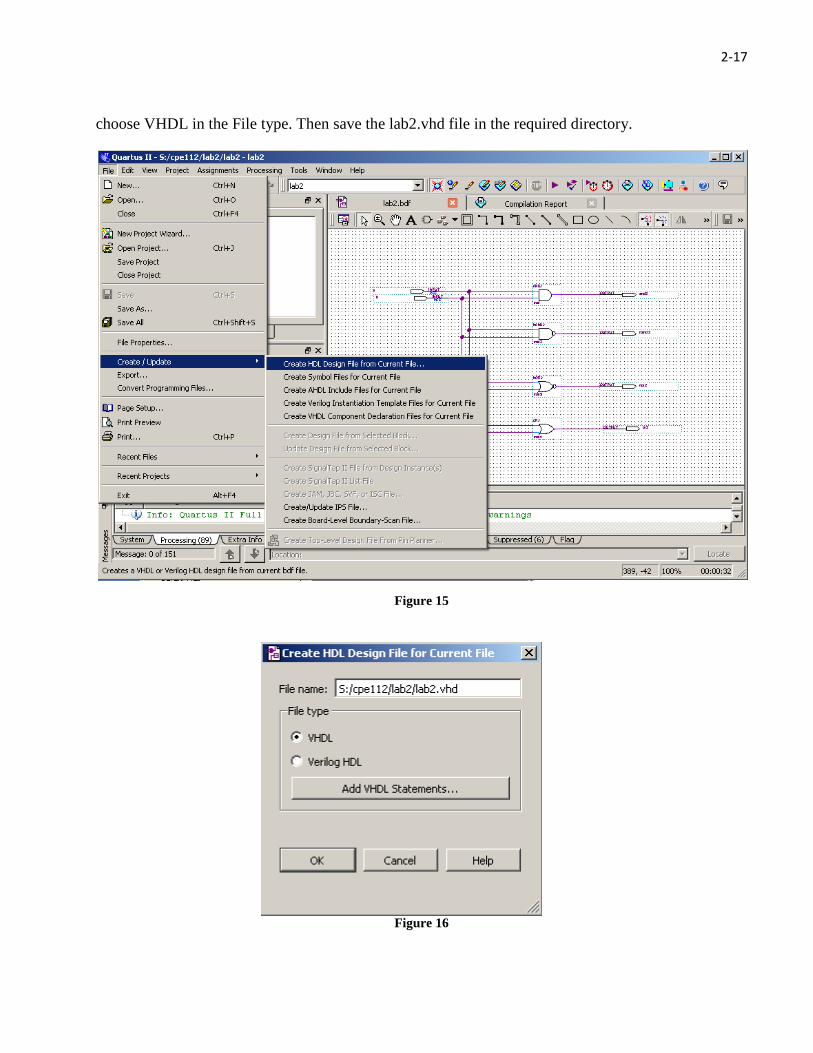
Once getting successful compilation, go to File, click Create/Update and Create HDL Design file from current file as shown in Figure 15. Another window (Figure 16) will pop up;
2-17
choose VHDL in the File type. Then save the lab2.vhd file in the required directory.
Figure 15
Figure 16
2-18
Tutorial
Simulation using ModelSim-Altera
VHSIC Hardware Description Language (VHDL) is an increasingly important tool in digital used for automated specification and testing of digital systems. You can create VHDL code automatically from the schematic in Quartus II.
You can perform a functional and/or a timing simulation of a Quartus II-generated design with the Mentor Graphics ModelSim-Altera software (OEM) or the ModelSim PE or SE (non-OEM) software. The ModelSim software is a dual-language simulator; you can simulate designs containing either Verilog HDL, VHDL, or both. You can use designs in which a Verilog HDL module instantiates VHDL entities or a VHDL module instantiates Verilog HDL entities.
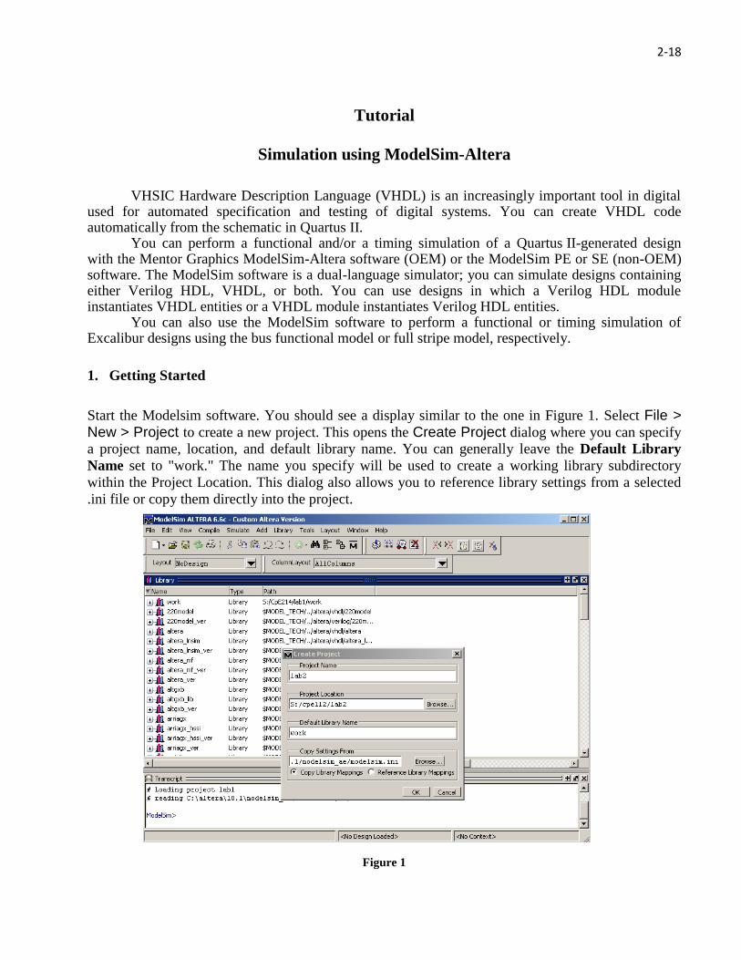
You can also use the ModelSim software to perform a functional or timing simulation of Excalibur designs using the bus functional model or full stripe model, respectively. 1. Getting Started Start the Modelsim software. You should see a display similar to the one in Figure 1. Select File > New > Project to create a new project. This opens the Create Project dialog where you can specify
a project name, location, and default library name. You can generally leave the Default Library
Name set to "work." The name you specify will be used to create a working library subdirectory
within the Project Location. This dialog also allows you to reference library settings from a selected
.ini file or copy them directly into the project.
Figure 1

2-19
After selecting OK, you will see a blank Project tab in the Workspace pane of the Main window
(Figure 2) and the Add Items to the Project dialog (Figure 3).
Figure 2
Figure 3
2. Adding Items to the Project The Add Items to the Project dialog includes these options:
Create New File — Create a new VHDL, Verilog, Tcl, or text file using the Source editor.
Add Existing File — Add an existing file. See below for details.
Create Simulation—Create a Simulation Configuration that specifies source files and
simulator options.
Create New Folder — Create an organization folder.
2-20
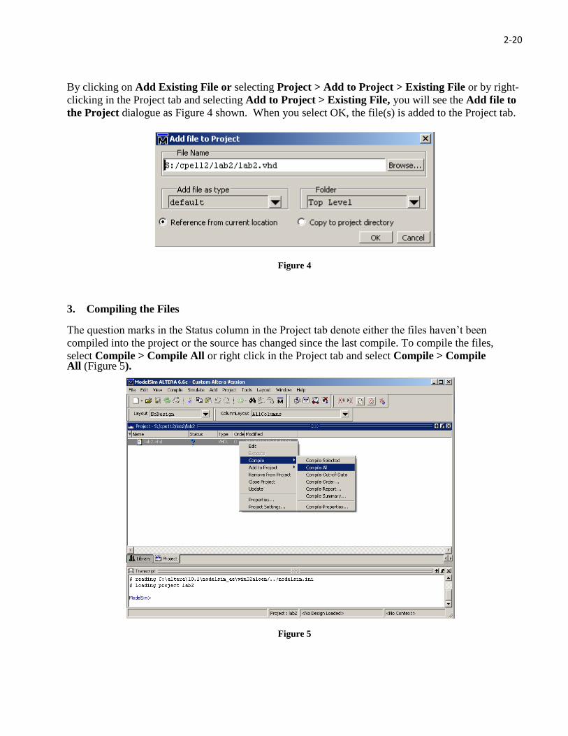
By clicking on Add Existing File or selecting Project > Add to Project > Existing File or by right-
clicking in the Project tab and selecting Add to Project > Existing File, you will see the Add file to
the Project dialogue as Figure 4 shown. When you select OK, the file(s) is added to the Project tab.
Figure 4
3. Compiling the Files The question marks in the Status column in the Project tab denote either the files haven’t been
compiled into the project or the source has changed since the last compile. To compile the files,
select Compile > Compile All or right click in the Project tab and select Compile > Compile All (Figure 5).
Figure 5
2-21
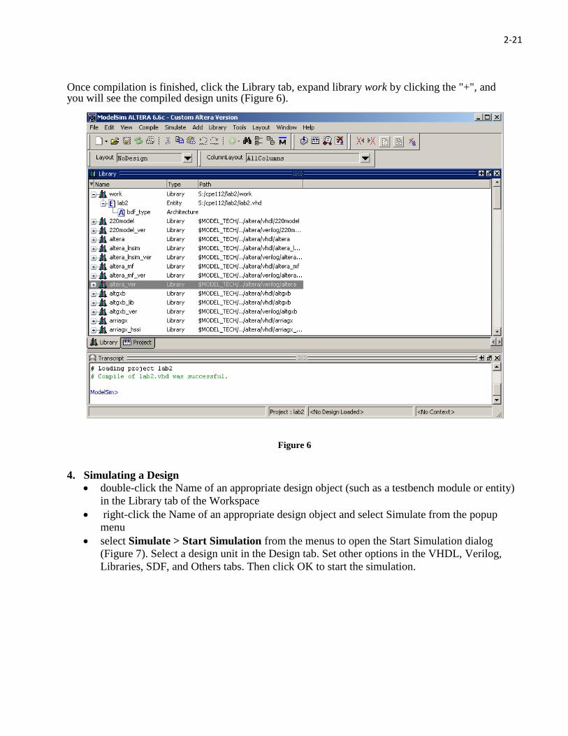
Once compilation is finished, click the Library tab, expand library work by clicking the "+", and you will see the compiled design units (Figure 6).
Figure 6
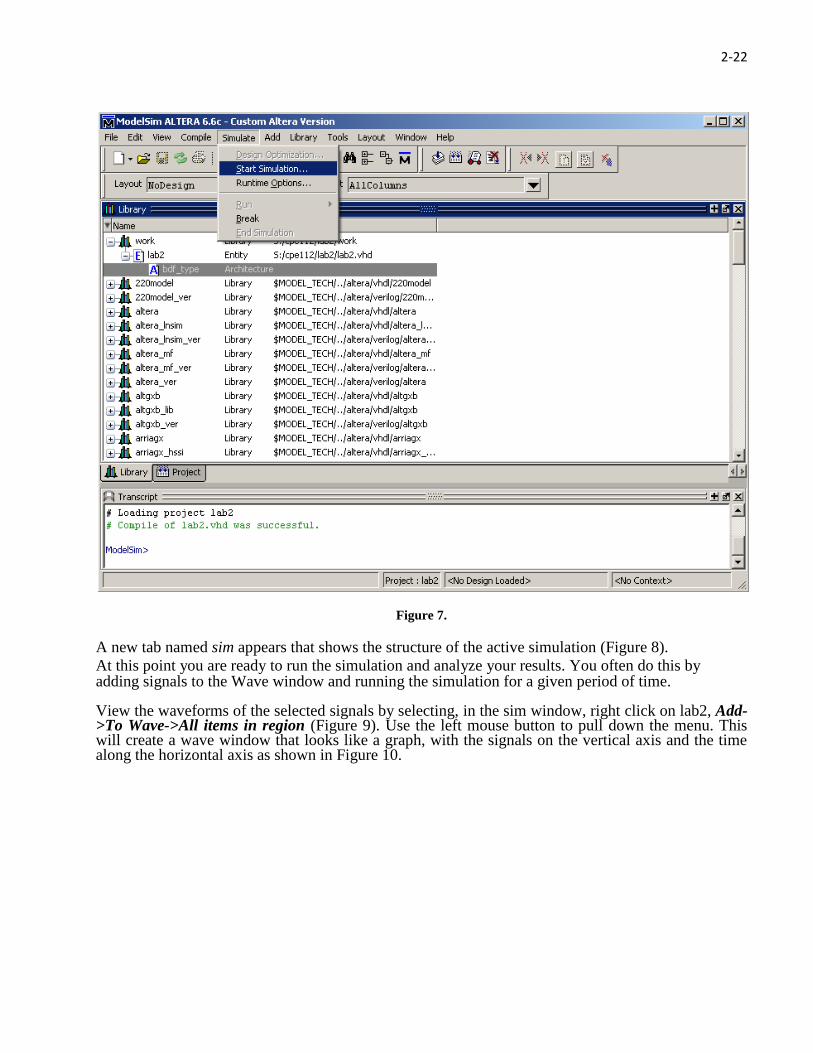
4. Simulating a Design
double-click the Name of an appropriate design object (such as a testbench module or entity)
in the Library tab of the Workspace
right-click the Name of an appropriate design object and select Simulate from the popup
menu
select Simulate > Start Simulation from the menus to open the Start Simulation dialog
(Figure 7). Select a design unit in the Design tab. Set other options in the VHDL, Verilog,
Libraries, SDF, and Others tabs. Then click OK to start the simulation.
2-22
Figure 7.
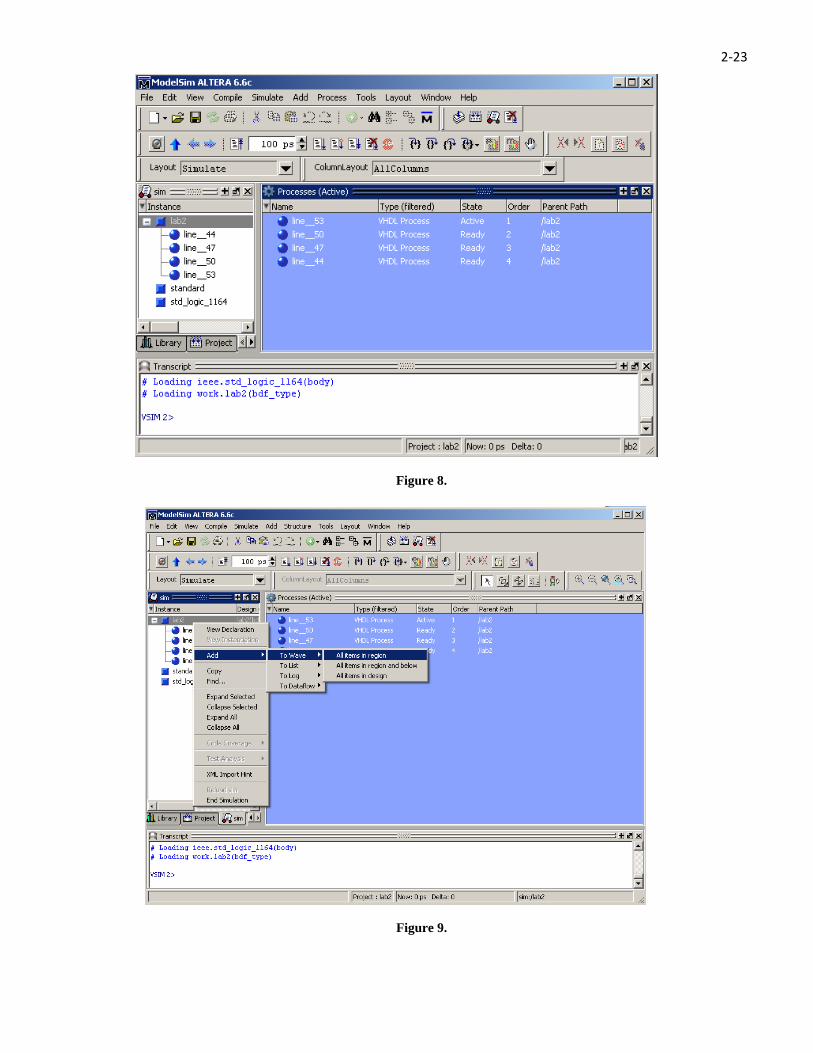
A new tab named sim appears that shows the structure of the active simulation (Figure 8).
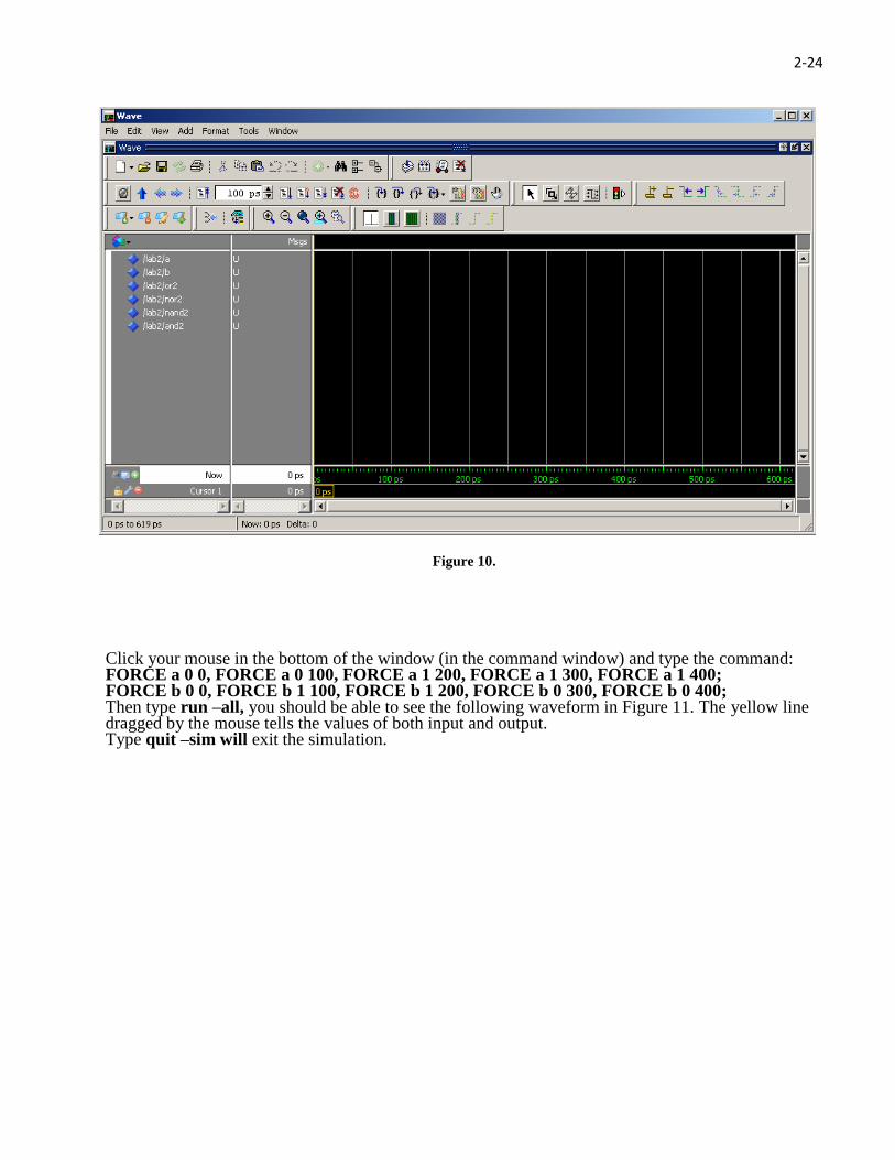
At this point you are ready to run the simulation and analyze your results. You often do this by adding signals to the Wave window and running the simulation for a given period of time. View the waveforms of the selected signals by selecting, in the sim window, right click on lab2, Add->To Wave->All items in region (Figure 9). Use the left mouse button to pull down the menu. This will create a wave window that looks like a graph, with the signals on the vertical axis and the time along the horizontal axis as shown in Figure 10.
2-23
Figure 8.
Figure 9.
2-24
Figure 10.
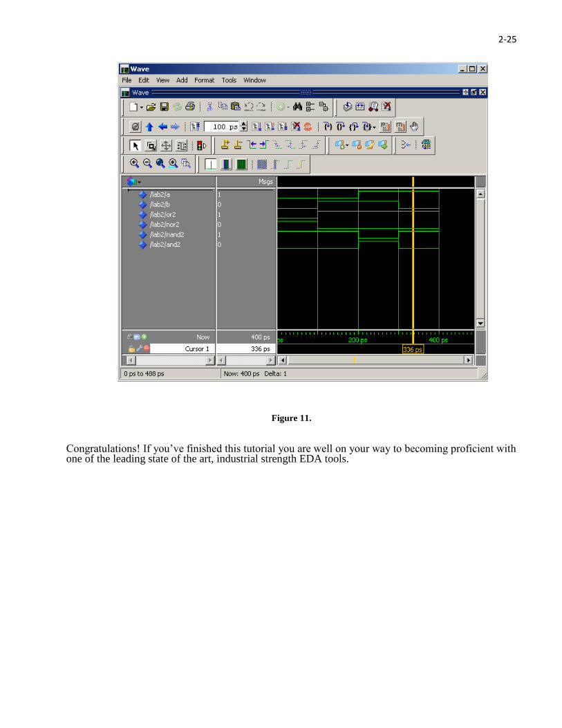
Click your mouse in the bottom of the window (in the command window) and type the command: FORCE a 0 0, FORCE a 0 100, FORCE a 1 200, FORCE a 1 300, FORCE a 1 400; FORCE b 0 0, FORCE b 1 100, FORCE b 1 200, FORCE b 0 300, FORCE b 0 400; Then type run –all, you should be able to see the following waveform in Figure 11. The yellow line dragged by the mouse tells the values of both input and output. Type quit –sim will exit the simulation.
2-25
Figure 11.
Congratulations! If you’ve finished this tutorial you are well on your way to becoming proficient with one of the leading state of the art, industrial strength EDA tools.