exg x-series signal generators n5171b analog & …...data sheet exg x-series signal generators...
TRANSCRIPT

D A T A S H E E T
EXG X-Series Signal GeneratorsN5171B Analog & N5172B Vector9 kHz to 1, 3, or 6 GHz9 kHz to 7.2 GHz 1
1. Only applicable to N5172B + N5182BX07 Frequency Extender

Page 2Find us at www.keysight.com
Definitions and conditions ............................................................................................................................2
Frequency specifications ..............................................................................................................................3
Amplitude specifications ..............................................................................................................................5
Spectral purity specifications .....................................................................................................................10
Analog modulation specifications ..............................................................................................................12
Vector modulation specifications - N5172B only .......................................................................................17
General specifications ................................................................................................................................28
Inputs and outputs .....................................................................................................................................29
Related literature ........................................................................................................................................31
Optimized for manufacturingOn the path to faster throughput and greater uptime, the cost-effective EXG X-Series signal generators are optimized for manufacturing test. With analog and vector models, the EXG provides the signals you’ll need for basic parametric testing of components and functional verification of receivers. Get “just enough” test at the right price with the EXG.
Table of Contents
Definitions and Conditions
Specifications represent warranted performance of a calibrated instrument that has been stored for a minimum of 2 hours within the operating temperature range of 0 to 55 °C, unless otherwise stated, and after a 45 minute warm-up period. The specifications include measurement uncertainty. Data represented in this document are specifications unless otherwise noted.
Typical (typ) describes additional product performance information. It is performance beyond specifications that 80 percent of the units exhibit with a 90 percent confidence level at room temperature (approximately 25 °C). Typical performance does not include measurement uncertainty.
Nominal (nom) values indicate the expect mean or average performance, or an attribute whose performance is by design, such as the 50 ohm connector. This data is not warranted and is measured at room temperature (approximately 25 °C).
Measured (meas) describes an attribute measured during the design phase for purposes of communicating expected performance, such as amplitude drift vs. time. This data is not warranted and is measured at room temperature (approximately 25 °C).
Page 3Find us at www.keysight.com
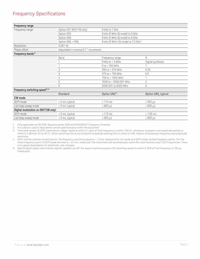
Frequency Specifications
Frequency rangeFrequency range Option 501 (N5171B only) 9 kHz to 1 GHz
Option 503 9 kHz (5 MHz IQ mode) to 3 GHzOption 506 9 kHz (5 MHz IQ mode) to 6 GHzOption 506 + FRQ 9 kHz (5 MHz I/Q mode) to 7.2 GHz1
Resolution 0.001 HzPhase offset Adjustable in nominal 0.1 ° incrementsFrequency bands 2
Band Frequency range N1 9 kHz to < 5 MHz Digital synthesis1 5 to < 250 MHz 12 250 to < 375 MHz 0.253 375 to < 750 MHz 0.54 750 to < 1500 MHz 15 1500 to < 3000.001 MHz 26 3000.001 to 6000 MHz 4
Frequency switching speed 3, 4
Standard Option UNZ 5 Option UNZ, typicalCW modeSCPI mode ≤ 5 ms, typical ≤ 1.15 ms ≤ 950 µsList/step sweep mode ≤ 5 ms, typical ≤ 900 µs ≤ 800 µsDigital modulation on (N5172B only)SCPI mode ≤ 5 ms, typical ≤ 1.15 ms ≤ 1.05 msList/step sweep mode ≤ 5 ms, typical ≤ 900 µs ≤ 800 µs
1. Only applicable to N5182B. Requires option 506 and N5182BX07 Frequency Extender.2. N is a factor used to help define certain specifications within the document.3. Time from receipt of SCPI command or trigger signal to within 0.1 ppm of final frequency or within 100 Hz, whichever is greater, and amplitude settled to
within 0.2 dB from 20 to 30 °C. When switching into or out of band 6 amplitude settling time is within 0.3 dB. Implies simultaneous frequency and amplitude switching.
4. With internal channel corrections on, the frequency switching speed is < 1.3 ms, measured for list mode and SCPI mode cached frequency points. For the initial frequency point in SCPI mode the time is < 3.3 ms, measured. The instrument will automatically cache the most recently used 1024 frequencies. There is no speed degradation for amplitude-only changes.
5. Specificationsapplywhenstatusregisterupdatesareoff.ForexportcontrolpurposesCWswitchingspeedtowithin0.05%offinalfrequencyis190μs(measured).
Page 4Find us at www.keysight.com
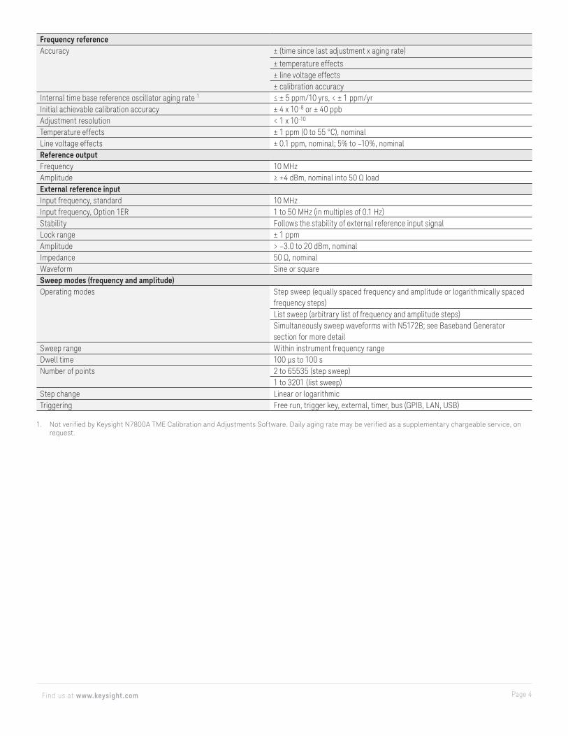
Frequency referenceAccuracy ± (time since last adjustment x aging rate)
± temperature effects± line voltage effects± calibration accuracy
Internal time base reference oscillator aging rate 1 ≤ ± 5 ppm/10 yrs, < ± 1 ppm/yrInitial achievable calibration accuracy ± 4 x 10⁻⁸ or ± 40 ppbAdjustment resolution < 1 x 10⁻¹⁰
Temperature effects ± 1 ppm (0 to 55 °C), nominalLine voltage effects ± 0.1 ppm, nominal; 5% to –10%, nominalReference outputFrequency 10 MHzAmplitude ≥ +4 dBm, nominal into 50 Ω loadExternal reference inputInput frequency, standard 10 MHzInput frequency, Option 1ER 1 to 50 MHz (in multiples of 0.1 Hz)Stability Follows the stability of external reference input signalLock range ± 1 ppmAmplitude > –3.0 to 20 dBm, nominalImpedance 50 Ω, nominalWaveform Sine or squareSweep modes (frequency and amplitude)Operating modes Step sweep (equally spaced frequency and amplitude or logarithmically spaced
frequency steps)List sweep (arbitrary list of frequency and amplitude steps)Simultaneously sweep waveforms with N5172B; see Baseband Generator section for more detail
Sweep range Within instrument frequency rangeDwell time 100 µs to 100 sNumber of points 2 to 65535 (step sweep)
1 to 3201 (list sweep)Step change Linear or logarithmicTriggering Free run, trigger key, external, timer, bus (GPIB, LAN, USB)
1. Not verified by Keysight N7800A TME Calibration and Adjustments Software. Daily aging rate may be verified as a supplementary chargeable service, on request.
Page 5Find us at www.keysight.com
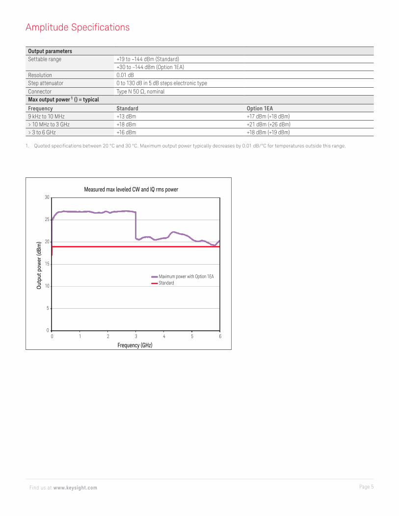
Output parametersSettable range +19 to –144 dBm (Standard)
+30 to –144 dBm (Option 1EA)Resolution 0.01 dBStep attenuator 0 to 130 dB in 5 dB steps electronic typeConnector Type N 50 Ω, nominalMax output power 1 () = typical
Frequency Standard Option 1EA9 kHz to 10 MHz +13 dBm +17 dBm (+18 dBm)> 10 MHz to 3 GHz +18 dBm +21 dBm (+26 dBm)> 3 to 6 GHz +16 dBm +18 dBm (+19 dBm)
1. Quoted specifications between 20 °C and 30 °C. Maximum output power typically decreases by 0.01 dB/°C for temperatures outside this range.
Amplitude Specifications
0
5
10
15
20
25
30
0 1 2 3 4 5 6
Out
put p
ower
(dB
m)
Frequency (GHz)
Measured max leveled CW and IQ rms power
Maximum power with Option 1EAStandard
Page 6Find us at www.keysight.com
Measured level accuracy at –140 dBm
Frequency (MHz)
Pow
er e
rror
(dB)
1
0.8
0.6
0.4
0.2
0
–0.2
–0.4
–0.6
–0.8
–10 1000 2000 3000 4000 5000 6000
Upper std dev (1 σ)MeanLower std dev (1 σ)
Measured level accuracy at –110 dBm
Frequency (MHz)
Pow
er e
rror
(dB)
1
0.8
0.6
0.4
0.2
0
–0.2
–0.4
–0.6
–0.8
–1
Upper std dev (1 σ)MeanLower std dev (1 σ)
0 1000 2000 3000 4000 5000 6000
Measurement level accuracy at –130 dBm
Frequency (MHz)
Pow
er e
rror
(dB)
1
0.8
0.6
0.4
0.2
0
–0.2
–0.4
–0.6
–0.8
–1
Upper std dev (1 σ)MeanLower std dev (1 σ)
0 1000 2000 3000 4000 5000 6000
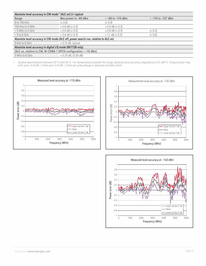
Absolute level accuracy in CW mode 1 (ALC on) ()= typicalRange Max power to –60 dBm < –60 to –110 dBm < –110 to –127 dBm9 to 100 kHz (± 0.6) (± 0.9)100 kHz to 5 MHz ± 0.8 dB (± 0.3) ± 0.9 dB (± 0.3)> 5 MHz to 3 GHz ± 0.6 dB (± 0.3) ± 0.8 dB (± 0.3) (± 0.5)> 3 to 6 GHz ± 0.6 dB (± 0.3) ± 1.1 dB (± 0.3) (± 0.6)Absolute level accuracy in CW mode (ALC off, power search run, relative to ALC on)9 kHz to 6 GHz ± 0.15 dB, typicalAbsolute level accuracy in digital I/Q mode (N5172B only)(ALC on, relative to CW, W-CDMA 1 DPCH configuration < +10 dBm)5 MHz to 6 GHz ± 0.25 dB, (0.05 dB)
1. Quoted specifications between 20 °C and 30 °C. For temperatures outside this range, absolute level accuracy degrades by 0.01 dB/°C. Output power may drift up to 0.10 dB < 3 GHz and 0.15 dB > 3 GHz per g/kg change in absolute humidity (nom).
Page 7Find us at www.keysight.com
0 20 40 60 80 100 120
0.5
0.4
0.3
0.2
0.1
0
–0.1
–0.2
–0.3
–0.4
–0.5
Elapsed time (minutes)
Delta
from
initi
al (d
B)
Measured amplitude repeatablity +5 dBm ALC on
850 MHz
1900 MHz
2200 MHz
3500 MHz
5800 MHz
Measured relative level accuracy at 850 MHz initial power +10 dBm
Final power (dBm)
Pow
er e
rror
(dB)
0 –20 –40 -60 –80 –100 –120 –140
0.5
0.4
0.3
0.2
0.1
0
–0.1
–0.2
–0.3
–0.4
–0.5
Upper std dev (1 σ)MeanLower std dev (1 σ)
Measured ALC linearity 1900 MHz, CW, relative to 0 dBm
Amplitude (dB)
–20 –15 –10 –5 0 5 10
0.3
0.2
0.1
0
–0.1
–0.2
–0.3
Erro
r (dB
)
Upper std dev (1 σ)MeanLower std dev (1 σ )
Measured ALC linearity850 MHz, CW, relative to 0 dBm
Amplitude (dB)
–20 –15 –10 –5 0 5 10
0.3
0.2
0.1
0
–0.1
–0.2
–0.3
Erro
r (dB
)
Upper std dev (1 σ)MeanLower std dev (1 σ)
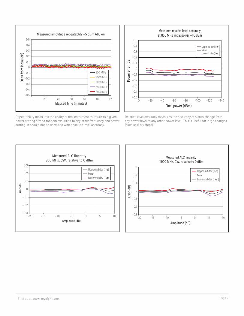
Repeatability measures the ability of the instrument to return to a given power setting after a random excursion to any other frequency and power setting. It should not be confused with absolute level accuracy.
Relative level accuracy measures the accuracy of a step change from any power level to any other power level. This is useful for large changes (such as 5 dB steps).
Page 8Find us at www.keysight.com
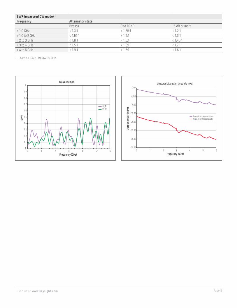
SWR (measured CW mode) 1
Frequency Attenuator stateBypass 0 to 10 dB 15 dB or more
≤ 1.0 GHz < 1.3:1 < 1.35:1 < 1.2:1> 1.0 to 2 GHz < 1.55:1 < 1:5:1 < 1.3:1> 2 to 3 GHz < 1.8:1 < 1.5:1 < 1.45:1> 3 to 4 GHz < 1.5:1 < 1.6:1 < 1.7:1> 4 to 6 GHz < 1.9:1 < 1.6:1 < 1.6:1
1. SWR < 1.60:1 below 30 kHz.
1
1.1
1.2
1.3
1.4
1.5
1.6
1.7
1.8
1.9
2
0 1 2 3 4 5 6
SW
R
Frequency (GHz)
Measured SWR
0 dB 15 dB
-35.00
-30.00
-25.00
-20.00
-15.00
-10.00
-5.00
0.00
0 1 2 3 4 5 6
Out
put p
ower
(dB
m)
Frequency (GHz)
Measured attenuator threshold level
Threshold for bypass attenuatorThreshold for 10 dB attenuator
Page 9Find us at www.keysight.com
Maximum reverse power, nominal< 1 GHz 50 W> 1 to 2 GHz 25 W> 2 to 6 GHz 20 WMax DC voltage 50 VDCTrip level 2 WAmplitude switching speed 1 Standard Option UNZ Option UNZ, typicalCW mode
– SCPI mode ≤ 5 ms, typical ≤ 750 µs ≤ 650 µs – Power search SCPI mode < 12 ms, measured
List/step sweep mode ≤ 5 ms, typical ≤ 500 µs ≤ 300 µsDigital modulation on (N5172B only)
– SCPI mode ≤ 5 ms, typical ≤ 1.15 ms ≤ 950 µs – Power search SCPI mode < 12 ms, measured – List/step sweep mode ≤ 5 ms, typical ≤ 900 µs ≤ 400 µs
Alternate power level control (N5172B only)Switching time(via waveform markers)
20 µs within ± 1 dB, measured
Functional power range –15 dBm to –144 dBm, measuredUser flatness correction
Number of points 3201Number of tables Dependent on available free memory in instrument; 10,000 maximumEntry modes USB/LAN direct power meter control, LAN to GPIB and USB to GPIB, remote bus and manual USB/GPIB power
meter controlSweep modes
See Frequency Specifications section for more detail
1. Time from receipt of SCPI command or trigger signal to amplitude settled within 0.2 dB. Switching speed specifications apply when status register updates are off.

Page 10Find us at www.keysight.com
Absolute SSB phase noise (dBc/Hz, CW at 20 kHz offset, typical)5 MHz to < 250 MHz –119250 MHz –133500 MHz –1281 GHz –1222 GHz –1153 GHz –1104 GHz –1096 GHz –103
Spectral Purity Specifications
-170
-160
-150
-140
-130
-120
-110
-100
-90
-80
-70
-60
-50
-40
-30
-20
10 Hz 100 Hz 1 kHz 10 kHz 100 kHz 1 MHz 10 MHz 100 MHz
L(f) [dBc/Hz] vs. frequency
Measured standard phase noise CW mode
6 GHz3 GHz2 GHz1 GHz250 MHz100 MHz
-170
-160
-150
-140
-130
-120
-110
-100
-90
-80
-70
-60
-50
-40
-30
-20
10 Hz 100 Hz 1 kHz 10 kHz 100 kHz 1 MHz 10 MHz 100 MHz
1 GHz
L(f) [dBc/Hz] vs. frequency
Measured absolute phase noise, S/N mode + 10 dBm
1 GHz 0 dBm1 GHz 0 dBm S/N1 GHz +23 dBm
-170
-160
-150
-140
-130
-120
-110
-100
-90
-80
-70
-60
-50
-40
-30
-20
10 Hz1 Hz 100 Hz 1 kHz 10 kHz 100 kHz 1 MHz 10 MHz 100 MHz
L(f) [dBc/Hz] vs. frequency
Measured AM noise @ 1 GHz S/N mode on/off, 2kHz ALC bandwidth
-170
-160
-150
-140
-130
-120
-110
-100
-90
-80
-70
-60
-50
-40
-30
-20
10 Hz 100 Hz 1 kHz 10 kHz 100 kHz 1 MHz 10 MHz 100 MHz
6 GHz3 GHz2 GHz1 GHz250 MHz100 MHz
L(f) [dBc/Hz] vs. frequency
Measured absolute phase noise with IQ modulation

Page 11Find us at www.keysight.com
Residual FM (CW mode, 300 Hz to 3 kHz BW, CCITT, rms)5 MHz to 6 GHz < N x 2 Hz (measured) (see N value in frequency band table)Residual AM (CW mode, 0.3 to 3 kHz BW, rms, +5 dBm)100 kHz to 3 GHz < 0.01% (measured)Harmonics (CW mode)Range Standard < +4 dBm Option 1EA < +12 dBm9 kHz to 3 GHz < –35 dBc < –30 dBc> 3 to 4 GHz < –35 dBc, typical < –35 dBc, typical> 4 to 6 GHz < –53 dBc, typical < –40 dBc, typicalNonharmonics (CW mode)Range > 10 KHz offset
Standard (dBc)9 kHz to < 5 MHz –65, nominal5 to < 250 MHz –75250 to < 750 MHz –75750 MHz to < 1.5 GHz –721.5 to < 3.0 GHz –663 to 6 GHz –60
Subharmonics (CW mode)9 kHz to 1.5 GHz None> 1.5 to 3 GHz –77 dBc> 3 to 6 GHz –74 dBcJitter 1
Carrier frequency SONET/SDH data rate rms jitter BW μUI rms, measured Seconds, typical155 MHz 155 MB/s 100 Hz to 1.5 MHz 140 0.9 ps622 MHz 622 MB/s 1 KHz to 5 MHz 67 0.11 ps2.488 GHz 2488 MB/s 5 kHz to 20 MHz 271 0.11 psPhase coherence (Option 012)LO input frequency range 250 MHz to 6 GHz, nominalLO input power range 0 to +12 dBm, nominalLO output frequency range 250 MHz to 6 GHz, nominalLO output power range 0 to +12 dBm, nominal
1. Calculated from phase noise performance in CW mode at +10 dBm. For other frequencies, data rates, or bandwidths, please consult your sales representative.
Page 12Find us at www.keysight.com
Analog Modulation Specifications
Frequency bandsBand # Frequency range N1 9 kHz to < 5 MHz 1 (digital synthesis)1 5 to < 250 MHz 12 250 to < 375 MHz 0.253 375 to < 750 MHz 0.54 750 to < 1500 MHz 15 1500 to < 3000.001 MHz 26 3000.001 to 6000 MHz 4Frequency modulation (Option UNT) (See N value above)Max deviation N × 10 MHz, nominal 3
Resolution 0.025% of deviation or 1 Hz, whichever is greater, nominalDeviation accuracy < ± 2% + 20 Hz (1 kHz rate, deviation is N x 50 kHz)Modulation frequency response at 100 KHz rate
1 dB bandwidth DC/5 Hz to 3 MHz, nominal3 dB bandwidth DC/1 Hz to 7 MHz, nominal
Carrier frequency accuracy < ± 0.2% of set deviation + (N × 1 Hz) 1
Relative to CW in DCFM < ± 0.06% of set deviation + (N × 1 Hz), typical 2
Distortion < 0.4% [1 kHz rate, deviation is N x 50 kHz]FM using external inputs 1 or 2 Sensitivity +1 V peak for indicated deviation, nominal
Input impedance 50 Ω/600 Ω/1 M Ω, nominalPaths FM path 1 and FM path 2 are summed internally for
composite modulationPhase modulation (Option UNT) (See N value above)Maximum deviation Normal bandwidth N × 5 radians, nominal
High-bandwidth mode N × 0.5 radians, nominalFrequency response Normal bandwidth (3 dB) DC to 1 MHz, nominal
High-bandwidth mode (3 dB) DC to 4 MHz, nominalResolution 0.1% of deviationDeviation accuracy < + 0.5% + 0.01 rad, typical [1 kHz rate, normal bandwidth mode]Distortion < 0.2% (typ) [1 kHz rate, deviation normal bandwidth mode]ΦM using external inputs 1 or 2 Sensitivity +1 V peak for indicated deviation, nominal
Input impedance 50 Ω or 600 Ω or 1 M Ω, nominalPaths ΦM path 1 and ΦM path 2 are summed internally
for composite modulation
1. Specification valid for temperature changes of less than ± 5 °C since last DCFM calibration.2. Typical performance immediately after a DCFM calibration.3. Digital synthesis band FM deviation is 5 MHz.
Page 13Find us at www.keysight.com
Amplitude modulation (Option UNT) 1
AM depth type Linear or exponentialMaximum depth 100%Depth resolution 0.1% of depth (nom)AM depth error at 1 KHz rate and < 80% depth
f < 5 MHz < 1.5% of setting + 1% (typ 0.5% of setting + 1%)5 MHz ≤ f ≤ 2 GHz < 3% of setting + 1 %2 < f < 3 GHz < 5% of setting + 1% (typical 3% of setting + 1%)3 < f < 6 GHz (typical 4% of setting + 1%)
Total harmonic distortion at 1 KHz rate
F < 5 MHz 30% depth < 0.25%, typical80% depth < 0.5%, typical
5 MHz ≤ f < 2 GHz(2 to 3 GHz is typical)
30% depth < 2%80% depth < 2%
Frequency response 30% depth, 3 dB BW DC/10 Hz to 50 KHzFrequency response wideband AM (N5172B only)
Rates ALC off/on: DC/800 Hz to 80 MHz, nominal
AM inputs using external inputs 1 or 2
Sensitivity ± 1 V peak for indicated depth (Over-range can be 200% or 2.2 V peak)Input impedance 50 Ω or 600 Ω or 1M Ω, Damage level: ± 5 V maxPaths AM path 1 and AM path 2 are summed internally for composite modulation
Wideband AM inputs(N5172B only)
Sensitivity 1 V peak-to-peak sine wave signal with 0.5 V DC offset required input for 100% AM
Input impedance 50 Ω, nominal (I input)Simultaneous and composite modulation 2
Simultaneous modulation All modulation types (I/Q, FM, AM, ΦM, and pulse modulation) may be simultaneously enabled except: FM and phase modulation cannot be combined and two modulation types cannot be simultaneously generated using the same modulation source; for example, the baseband I/Q generator, AM, and FM can run concurrently and all will modulate the output RF (this is useful for simulating signal impairments)
Composite modulation AM, FM, and ΦM each consist of two modulation paths which are summed internally for composite modulation; modulation can be any combination of internal or external sourcesAM FM Phase Pulse Internal I/Q 2 External I/Q 2
AM + + + + + +FM + + – + + +Phase + – + + + +Pulse + + + – + +Internal I/Q 2 + + + + * +External I/Q 2 + + + + + –+ = compatible, – = incompatible, * = Internal + External
1. AM specifications apply 6 dB below maximum specified power from 20 to 30 °C.2. I/Q modulation available on N5172B.
Page 14Find us at www.keysight.com
External modulation inputs(Option UNT required for FM, AM, and phase modulation inputs; Option UNW required for pulse modulation inputs)EXT1 AM, FM, PMEXT2 AM, FM, PMPULSE Pulse (50 Ω only)I Wideband AM (50 Ω only, N5172B only)Input impedance 50 Ω, 1 MΩ, 600 Ω, DC and AC coupledStandard internal analog modulation source(Single sine wave generator for use with AM, FM, phase modulation requires Option UNT or 303)Waveform Sine, square, triangle, positive ramp, negative rampRate range 0.1 Hz to 2 MHz (tunable to 3 MHz)Resolution 0.1 HzFrequency accuracy Same as RF reference source, nominalLF audio output 0 to 5 V peak into 50 Ω, –5 V to 5 V offset, nominalMultifunction generator (Option 303)The multifunction generator option (Option 303) consists of seven waveform generators that can be set independently with up to five simultaneously using the composite modulation features in AM, FM/PM, and LF outWaveformFunction generator 1 Sine, triangle, square, positive ramp, negative ramp, pulseFunction generator 2 Sine, triangle, square, positive ramp, negative ramp, pulseDual function generator Sine, triangle, square, positive ramp, negative ramp, phase offset, and amplitude ratio for Tone 2
relative to Tone 1Swept function generator Sine, triangle, square, positive ramp, negative ramp
Trigger: free run, trigger key, bus, external, internal, timer triggerNoise generator 1 Uniform, GaussianNoise generator 2 Uniform, GaussianDC Only for LF output –5 V to +5 V, nominalFrequency parametersSine wave 0.1 Hz to 10 MHz, nominalTriangle, square, ramp, pulse 0.1 Hz to 1 MHz, nominalNoise bandwidth 10 MHz, nominalResolution 0.1 HzFrequency accuracy Same as RF reference source, nominalNarrow pulse modulation (Option UNW) 1 () = typicalOn/off ratio (> 80 dB)Rise/fall times (Tr, Tf) < 10 ns; (7 ns)Minimum pulse width ALC on/off ≥ 2 us/≥ 20 nsRepetition frequency ALC on/off 10 Hz to 500 kHz/DC to 10 MHzLevel accuracy (relative to CW) ALC on/off 2 < ± 1.0 dB (± 0.5) dB/(< ± 0.5) dBWidth compression (RF width relative to video out) (< 5 ns)
1. Pulse specifications apply to frequencies > 100 MHz and power set to > -3 dBm. Operable down to 9 kHz.2. With power search on.
Page 15Find us at www.keysight.com
Video feed-through 1 ≤ 3 GHz/> 3 GHz (< 50 mV/< 5 mV)External video delay (ext input to video) 30 ns, nominalRF delay (video to RF output) 20 ns, nominalPulse overshoot (< 15%)Input level +1 Vpeak = RF on into 50 Ω, nominalTd video delay (variable)Tw video pulse width (variable)Tp pulse period (variable)Tm RF delayTrf RF pulse widthTf RF pulse fall timeTr RF pulse rise timeVor pulse overshootVf Video feedthrough
SyncOutput
VideoOutput
RF PulseOutput
Td
Tm
Tw
Trf
Vf
TfTr
Vor
Tp
50%
50%
10%
90%
50%
Internal pulse generator (included with Option UNW)Modes Free-run, square, triggered, adjustable doublet, trigger doublet, gated, and external pulseSquare wave rate 0.1 Hz to 10 MHz, 0.1 Hz resolution, nominalPulse period 30 ns to 42 seconds, nominalPulse width 20 ns to pulse period –10 ns, nominalResolution 10 nsAdjustable trigger delay (–pulse period + 10 ns) to (pulse width –10 ns)Settable delay Free run –3.99 to 3.97 µs
Triggered 0 to 40 sResolution (delay, width, period) 10 ns, nominalPulse doublets 1st pulse delay (Relative to sync out) 0 to 42 s – pulse width – 10 ns
1st pulse width 500 ns to 42 s – delay – 10 ns2nd pulse delay 0 to 42 s – (Delay 1 + Width 2) – 10 ns2nd pulse width 20 ns to 42 s – (Delay 1 + Delay 2) – 10 ns
Pulse train generator Option 320 (requires Option UNW)Number of pulse patterns 2047On/off time range 20 ns to 42 sec
1. Video feed through applies to power levels < +10 dBm.

Page 16Find us at www.keysight.com
Avionics (Option 302)VORBearing accuracy ± 0.1 degreesFrequency accuracy Same as RF reference source, nominalAM accuracy 30% depth ± 5% of settingAM distortion 2%FM accuracy 480 Hz deviation ± 1.7 HzILS: localizer and glide slopeAM accuracy 40% depth ± 5% of settingAM distortion 2%Difference in depth of modulation (DDM) resolution Localizer 0.0002
Glide slope 0.0004Difference in depth of modulation (DDM) accuracy Localizer ± 0.0004 ± 5% of DDM 1
Glide slope ± 0.0008 ± 5% of DDM 1
Marker beaconMarker tone AM accuracy 95% depth ± 5% of setting + 1%Marker tone AM distortion 95% depth 5%
1. DDM must not be equal to 0.

Page 17Find us at www.keysight.com
Vector Modulation Specifications
N5172B only
I/Q modulator external inputs 1
Bandwidth Baseband (I or Q) Up to 100 MHz baseband, nominalRF (I+Q) Up to 200 MHz RF, nominal
I or Q offset ± 100 mV (200 uV resolution)I/Q gain balance ± 4 dB (0.001 dB resolution)I/Q attenuation 0 to 50 dB (0.01 dB resolution)Quadrature angle adjustment ± 200 unitsFull scale input drive (I+Q) 0.5 V into 50 Ω, nominalInternal I/Q baseband generator adjustments 1, 2 (Options 653, 655, and 657)I/Q offset ± 20% (0.025% dB resolution)I/Q gain ± 1 dB (0.001 dB resolution)Quadrature angle adjustment ± 10 ° (0.01 degrees resolution)I/Q phase ± 360.00 ° (0.01 degrees resolution)I/Q skew ± 500 ns (1 picosecond resolution)I/Q delay ± 250 ns (1 picosecond resolution)External I/Q outputs 1
Impedance 50 Ω, nominal per output100 Ω, nominal differential output
Type Single-ended or differential (Option 1EL)Maximum voltage per output 1 V peak-to-peak or 0.5 V peak; into 50 Ω (200 uV resolution)Bandwidth (I, Q) Baseband (I or Q) 80 MHz, nominal (Option 653, 655, and 657)
RF (I+Q) 160 MHz, nominal (Option 653, 655, and 657)Amplitude flatness ± 0.2 dB measured with channel corrections optimized for I/Q outputPhase flatness ± 2.5 degrees measured with channel corrections optimized for I/Q outputCommon mode I/Q offset ± 1.5 V into 50 Ω (200 uV resolution)Differential mode I or Q offset ± 50 mV into 50 Ω (200 uV resolution)
1. I/Q adjustments represent user interface nominal parameter ranges and not specifications.2. Internal I/Q adjustments apply to RF out and I/Q outputs simultaneously.
-200 -150 -100 -50 0 50 100 150 200
3
1
-1
-3
-5
-7
-9
-11
-13
-15
Frequency offset from carrier (MHz)
Measured external I/Q bandwidth
dB
5800 MHz3500 MHz2200 MHz1900 MHz1800 MHz850 MHz
60.0040.0020.00-20.00-40.00-60.00 0.00
Nor
mal
ized
pow
er (
dB)
Frequency offset (MHz)
Measured RF I/Q channel flatness using internal baseband generator (EXG factory channel correctons ON)
-0.50
-0.40
-0.30
-0.20
-0.10
0.10
0.20
0.30
0.40
0.50
0.00
850 MHz1000 MHz1800 MHz1900 MHz2200 MHz5800 MHz
Page 18Find us at www.keysight.com
Internal real-time complex digital I/Q filters (included with Option 653)Factory channel correction (256 taps)Corrects the linear phase and amplitude response of the baseband I/Q and RF outputs of the signal generator using factory calibration arrays (default mode is off).RF amplitude flatness (160 MHz) ± 0.2 dB measuredRF phase flatness (160 MHz) ± 2 degrees measuredUser channel correction (256 taps)Automated routine uses USB power sensor to correct for linear phase and amplitude response of DUT (equalizer). See User Guide for more details.Max RF amplitude flatness correction ± 15 dBMax RF phase flatness correction ± 20 degreesEqualization filter (256 taps)User can download and apply inverse or custom phase and amplitude response coefficients from tools such as MATLAB, 89600 VSA, or SystemVue to correct for linear errors of DUT/system. See User Guide for more details.Baseband generator (Options 653 and 655)Channels 2 [I and Q]Resolution 16 bits [1/65,536]Sample rate Option 653 100 Sa/s to 75 MSa/s
Option 653 and 655 100 Sa/s to 150 MSa/sOption 653, 655, and 657 100 Sa/s to 200 MSa/s
RF (I+Q) bandwidth Option 653 60 MHz, nominalOption 653 and 655 120 MHz, nominalOption 653, 655, and 657 160 MHz, nominal
Interpolated DAC rate 800 MHz (waveforms only need OSR = 1.25)Frequency offset range ± 80 MHzDigital sweep modes In list sweep mode each point in the list can have independent waveforms (N5172B) along with user
definable frequencies and amplitudes; see the Amplitude and Frequency Specifications sections for more detail.
Waveform switching speed 1 SCPI mode ≤ 5 ms, measured (standard)≤ 1.2 ms, measured (Option UNZ)
List/step sweep mode ≤ 5 ms, measured (standard)≤ 900 us, measured (Option UNZ)
Waveform transfer rates(measured, no markers, unencrypted)
FTP LAN to internal SSD 10.7 MB/sec or 2.67 Msa/secInternal SSD to FTP LAN 7.7 MB/sec 1.92 Msa/secFTP LAN to BBG 8.2 MB/sec or 2.05 Msa/secFTP LAN to BBG encrypted 4 MB/sec or 1 Msa/secUSB to BBG 19 MB/sec or 4.75 Msa/secBBG to USB 1.2 MB/sec or 300 Ksa/secInternal SSD to BBG 48 MB/sec or 12 Msa/secBBG to internal SSD 1.2 MB/sec or 300 Ksa/secSD card to BBG (Option 006)BBG to SD card (Option 006) 845 KB/sec or 211 Ksa/sec
1. SCPImodeswitchingspeedapplieswhenwaveformsarepre-loadedinlistsweepandsamplerate≥10MSa/s.

Page 19Find us at www.keysight.com
Arbitrary waveform memory Maximum playback capacity
32 Msa (standard)256 Msa (Option 021)512 Msa (Option 022)
Maximum storage capacity including markers
3 GBytes/800 Msa (standard)30 GBytes/7.5 Gsa (Option 009)8 GBytes / 2 Gsa (Option 006)
Waveform segments Segment length 60 samples to 32 Msa (standard)60 samples to 256 Msa (Option 021)60 samples to 512 Msa (Option 022)
Minimum memory allocation per segment
256 samples
Maximum number of segments
8192
Waveform sequences Maximum number of sequences
> 2000 depending on non-volatile memory usage
Maximum number of segments/sequence
32,000 (standard)4 million (Option 021 or 022)
Maximum number of repetitions
65,535
Triggers Types Continuous, single, gated, segment advanceSource Trigger key, external, bus (GPIB, LAN, USB)Modes Continuous Free run, trigger and run, reset and run
Single No retrigger, buffered trigger, restart on triggerGated Negative polarity or positive polaritySegment advance Single or continuous
External coarse delay time 5 ns to 40 sExternal coarse delay resolution 5 nsTrigger latency (Single trigger only) 356 ns + 1 sample clock period, nominalTrigger accuracy (Single trigger only) ± 2.5 ns, nominalSingle trigger - restart on trigger mode will initiate a FIFO clear. Therefore, the latency includes re-filling the buffer. The latency is 8 µs + (1406 x sample period) ± 1 sample clock period, nominal
Multi-baseband generator synchronization mode (multiple sources)
Fan out 1 master and up to 15 slavesTrigger repeatability < 1 ns, nominalTrigger accuracy Same as normal modeTrigger latency Same as normal modeFine trigger delay range See Internal I/Q Baseband sectionFine trigger delay resolution See Internal I/Q Baseband sectionI/Q phase adjustment range See Internal I/Q Baseband section
Markers Markers are defined in a segment during the waveform generation process, or from the front panel; a marker can also be routed to the RF blanking, ALC hold functions, and alternate amplitude; see Users Guide for more informationMarker polarity Negative, positiveNumber of markers 4RF blanking/burst on/off ratio > 80 dBAlternate amplitude control switching speed See amplitude section
Page 20Find us at www.keysight.com
Real-time modulation FIR filter: Nyquist, root-Nyquist, WCDMA, EDGE, Gaussian, rectangular, APCO25 C4FM, IS-95, User FIR(Applies real-time FIR filtering when playing waveforms with OSR=1. Helps reduce waveform size for long simulation times. Option 660 not required).
Real-time baseband generator (Option 660)Real-time baseband generator required for real-time Signal Studio applications 1
Cellular real-time applications LTE-FDD, LTE-TDD, HSPA+/W-CDMA, GSM/EDGE, cdma2000®
Real-time navigation GPS, GLONASS, GalileoReal-time video applications DVB-T/T2/H/S/S2/C/J.83 Annex A/C, ISDB-T/Note: Option 660 is not required for real-time custom modulation (Option 431)Memory: Shares memory with Options 653, 655, and 657Triggering: Same as Options 653, 655, and 657Markers: 3 markers available, all other features are same as Options 653, 655, and 657
Digital baseband inputs/outputs (Option 003/004)Options 003 and 004 activate the rear panel digital I/Q bus and enables connectivity to the N5102A digital signal interface module. In output mode (003), you can deliver realistic complex-modulated signals such as LTE, GPS, WLAN, custom pulses and many others directly to your digital devices and subsystems. In the input mode (004), the interface module ports your digital input to the signal generator's baseband system, providing a quick and easy way of upconverting to calibrated analog I/Q, IF, or RF frequencies. In both operating modes, the interface module adapts to your device with the logic type, data format, clock features, and signaling you require.Data (requires N5102A)Digital data format User-selectable: 2's complement or binary offset, I/Q (I, I-bar, Q, Q-bar) or digital IF output (real, imaginary)Data port Dual 16-bit data buses support parallel, parallel I/Q interleaved, parallel QI interleaved, or serial port
configurationN5102A connectors (breakout boards) 144-pin Tyco Z-Dok+ connects to break-out boards (included with N5102A) that interface with the following
connector types: 68-pin SCSI, 38-pin dual AMP Mictor, 100-pin dual Samtec, 20-pin dual 0.1 inch headers, 40-pin dual 0.1 inch headers
Logic types Single-ended: LVTTL, 1.5V CMOS, 1.8V CMOS, 2.5V CMOS, 3.3.V CMOS Differential: LVDS
Data output resampling EXG baseband output is resampled to the arbitrary clock rate set by the user via real-time curve-fit calculations.
1. See www.keysight.com/find/signalstudio for more information.
Page 21Find us at www.keysight.com
Clock (requires N5102A)Clock input User selectable: internal clock, device under test clock, or external clock (via SMA or breakout board)
N5102A SMA Ext Clock In connector: 50 Ω, 0 dBm nominal, 1 to 400 MHzClock output User selectable: via breakout board or SMA Clock Out connector
N5102A SMA Clock Out connector: 2 Vpp into load > 5 KΩ from 1 to 100 kHz, 400 mVpp into 50 Ω load from 100 kHz to 400 MHz
Sample rate (limited by EXG sample rate)
User-selectable in parallel mode up to a maximum 200 MHz, but limited by other user settings (see N5102A users guide for more details).User-selectable in serial mode, the maximum rate is 400 MHz/word size.
Bit rate (limited by EXG sample rate) Parallel Up to 200 MHz x word size (1.6 Gbps LVDS, CMOS and LVTTL) per parallel bus, 2 parallel buses availableSerial Up to 400 MHz per serial line (400 Mbps LVDS) or 150 MHz per serial line (150 Mbps (CMOS/LVTTL) 32 lines available
Clocks per sample In parallel output mode, the data sample can be held for 1, 2 or 4 clock cyclesClock to data skew Coarse adjustment in 90° steps from 0 to 270º; fine-adjustment in increments of 100 ps up to 5 nsClock polarity Clock signals may be invertedFrequency reference input 1 to 100 MHz BNC, 50 Ω, 3 dBm ± 6 dBPower supply (included on N5102A) Output: 5 V, 4 A DCAWGN (Option 403)Type Real-time, continuously calculated, and played using DSPModes of operation Standalone or digitally added to signal played by arbitrary waveform or real-time baseband generatorBandwidth With Option 653 1 Hz to 60 MHz
With Option 653 and 655 1 Hz to 120 MHzWith Option 653, 655, and 657 1 Hz to 160 MHz
Crest factor 15 dBRandomness 90 bit pseudo-random generation, repetition period 313 x 109 yearsCarrier-to-noise ratio ± 100 dB when added to signalCarrier-to-noise ratio formats C/N, Eb/NoCarrier-to-noise ratio error Magnitude error ≤ 0.2 dB at baseband I/Q outputsCustom modulation Arb Mode (Option 431)Modulation PSK BPSK, QPSK, OQPSK, π/4DQPSK, gray coded and unbalanced QPSK,
8PSK, 16PSK, D8PSKQAM 4, 16, 32, 64, 128, 256, 1024 (and 89600 VSA mappings)FSK Selectable: 2, 4, 8, 16, C4FMMSK 0 to 100°ASK 0 to 100%
Multicarrier Number of carriers Up to 100 (limited by a max bandwidth of 160 MHz depending on symbol rate and modulation type)
Frequency offset (per carrier) Up to –80 to +80 MHzPower offset (per carrier) 0 dB to –40 dB
Symbol rate 50 sps to 100 MspsFilter types Nyquist, root-Nyquist, Gaussian, rectangular, APCO 25 C4FM, userQuick setup modes APCO 25w/C4FM, APCO25 w/CQPSK, Bluetooth®, CDPD, DECT, EDGE, GSM, NADC, PDC, PHS, PWT, TETRAData Random only

Page 22Find us at www.keysight.com
Custom modulation real-time mode (Option 431) (Does not require Option 660)Modulation PSK BPSK, QPSK, OQPSK, π/4DQPSK, gray coded and unbalanced QPSK, 8PSK,
16PSK, D8PSK, IS95 QPSK, IS95 OQPSK, EDGE, HDQPSK, SOQPSKQAM 4, 16, 32, 64, 128, 256, 1024 (and 89600 VSA mappings)FSK Selectable 2,4,8, 16 level symmetric, C4FM, HCPM
User-defined Custom map of up to 16 deviation levelsMax deviation 20 MHz
MSK 0 to 100°ASK 0 to 100%DVB-S2 APSK 16APSK 2/3, 16APSK 3/4, 16APSK 4/5, 16APSK 5/6, 16APSK 8/9, 16APSK
9/10, 32APSK 3/4, 32APSK 4/5, 32APSK 5/6, 32APSK 8/9, 32APSK 9/10Custom I/Q Custom map of 1024 unique values
Frequency offset Up to –80 MHz to +80 MHzSymbol rate Internal generated data 1 sps to 100 Msps and max of 10 bits per symbol (Option 653 + 655 + 657)
External serial data 1 sps to [(50 Mbits/sec)/(#bits/symbol)]Filter types Selectable Nyquist, root-Nyquist, Gaussian, rectangular, APCO 25 (phase 1 and 2 UL and
DL), IS-95, WCDMA, EDGE (wide and HSR)IS-95 w/EQ, IS-95 Mod, IS-95 Mod w/EQ, HDQPSK, APCO25 HCPM, SOQPSK-TG
Custom FIR 16-bit resolution, up to 64 symbols long, automatically resampled to 1024 coefficients (max)> 32 to 64 symbol filter: symbol rate ≤ 12.5 MHz> 16 to 32 symbol filter: symbol rate ≤ 25 MHzInternal filters switch to 16 tap when symbol rate is between 25 and 100 MHz
Quick setup modes APCO 25 with (C4FM, CQPSK, HCPM, HDQPSK), TETRA , Bluetooth, CDPD, DECT, EDGE, GSM, NADC, PDC, PHS, PWT, WorldSpace, Iridium, ICO, CT2, TFTS16APSK 2/3, 16APSK 3/4, 16APSK 4/5, 16APSK 5/6, 16APSK 8/9, 16APSK 9/10, 32APSK 3/4, 32APSK 4/5, 32APSK 5/6, 32APSK 8/9, 32APSK 9/10, SOQPSK
Trigger delay Range 0 to 1,048,575 bitsResolution 1 bit
Data types Internally generated Pseudo-random patterns PN9, PN11, PN15, PN20, PN23Repeating sequence Any 4-bit sequence
Direct-pattern RAM [PRAM] max sizeNote: Used for custom TDMA/non-standard framing
32 Mb (standard)512 Mb (Option 021)1024 Mb (Option 022)
User file 32 MB (standard)256 MB (Option 021)512 MB (Option 022)
Externally streamed data (via AUX I/O)
Type Serial dataInputs/outputs Data, symbol sync, bit clock
Internal burst shape (varies with bit rate)
Rise/fall time range Up to 30 bitsRise/fall delay range –15 to +15 bits
Page 23Find us at www.keysight.com
3GPP W-CDMA distortion performance 1, 2
Standard Option UNV Option UNV with Option 1EA
Power level ≤ 2 dBm 2 ≤ 2 dBm 2 ≤ 5 dBm 2
Offset Configuration Frequency Spec Typ Spec Typ Spec TypAdjacent (5 MHz)
1 DPCH, 1 carrier 1800 to 2200 MHz– 69 dBc –73 dBc –71 dBc –75 dBc –71 dBc –75 dBc
Alternate (10 MHz) –70 dBc –75 dBc –72 dBc –77 dBc –71 dBc –77 dBcAdjacent (5 MHz) Test model 1 with
64 DPCH, 1 carrier1800 to 2200 MHz
–68 dBc –70 dBc –71 dBc –73 dBc –71 dBc –72 dBcAlternate (10 MHz) –73 dBc –72 dBc –76 dBc –71 dBc –76 dBcAdjacent (5 MHz) Test model 1 with
64 DPCH, 4 carrier1800 to 2200 MHz
–63 dBc –65 dBc –65 dBc –67 dBc –64 dBc –66 dBcAlternate (10 MHz) –64 dBc –66 dBc –66 dBc –68 dBc –66 dBc –68 dBc
1. ACPR specifications apply when the instrument is maintained within ± 20 to 30 °C.2. This is rms power. Convert from rms to peak envelope power (PEP) with the following equation: PEP = rms power + crest factor (for example, 3GPP test
model 1 with 64 DPCH has a crest factor 11.5 dB, therefore at +5 dBm rms, the PEP = 5 dBm + 11.5 dB = +16.5 dBm PEP).
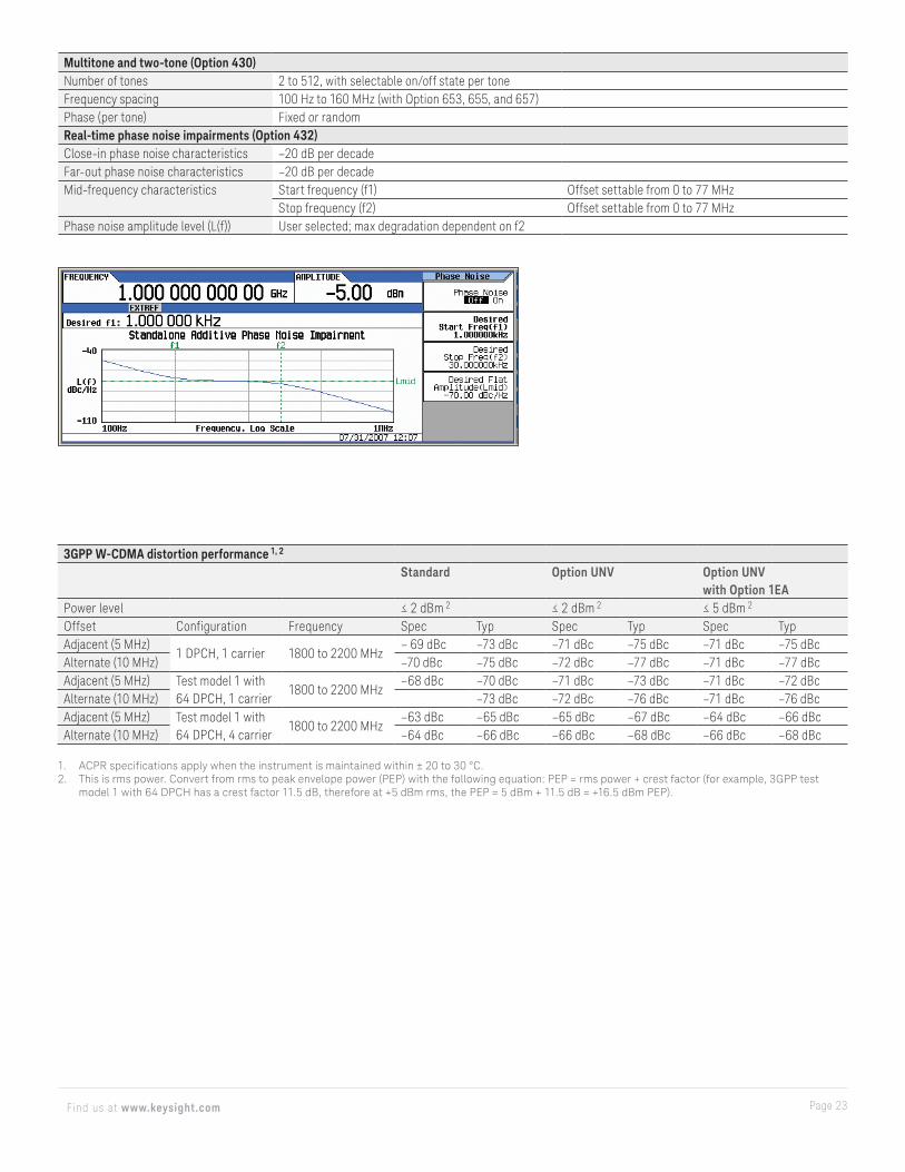
Multitone and two-tone (Option 430)Number of tones 2 to 512, with selectable on/off state per toneFrequency spacing 100 Hz to 160 MHz (with Option 653, 655, and 657)Phase (per tone) Fixed or randomReal-time phase noise impairments (Option 432)Close-in phase noise characteristics –20 dB per decadeFar-out phase noise characteristics –20 dB per decadeMid-frequency characteristics Start frequency (f1) Offset settable from 0 to 77 MHz
Stop frequency (f2) Offset settable from 0 to 77 MHzPhase noise amplitude level (L(f)) User selected; max degradation dependent on f2

Page 24Find us at www.keysight.com
-78
-76
-74
-72
-70
-66
-68
-10 -5 0 5 10
ACLR
(dB
c)
Power level (dBm)
Measured single carrier 3GPP W-CDMA ACLR TM1(with Option UNV + 1EA)
64 DPCH1 DPCH
-72
-70
-68
-66
-64
-62
-60
-10 -5 0 5 10
ACLR
(dB
c)
Power level (dBm)
Measured 4 carrier 3GPP W-CDMA ACLR TM1 64 DPCH(with Option UNV +1EA)
3GPP LTE-FDD distortion performance 1
Standard Option UNV Option UNV with Option 1EA
Power level ≤ 2 dBm 2 ≤ 2 dBm 2 ≤ 5 dBm 2
Offset Configuration Frequency Spec Typ Spec Typ Spec TypAdjacent (10 MHz) 3 10 MHz E-TM 1.1
QPSK1800 to 2200 MHz –64 dBc –66 dBc –67 dBc –69 dBc –64 dBc –67 dBc
Alternate (20 MHz) 3 –66 dBc –68 dBc –69 dBc –71 dBc –69 dBc –71 dBc
1. ACPR specifications apply when the instrument is maintained within ± 20 to 30 °C.2. This is rms power. Convert from rms to peak envelope power with the following equation: PEP = rms power + crest factor (for example, 3GPP test model 1
with 64 DPCH has a crest factor 11.5 dB, therefore at +5 dBm rms, the PEP = 5 dBm + 11.5 dB = +16.5 dBm PEP).3. ACPR measurement configuration: reference channel integration BW: 9.015 MHz, offset channel integration bandwidth: 9.015 MHz.
-78
-76
-74
-72
-70
-68
-66
-64
-62
-60
-10 -5 0 5 10
ACLR
(dBc
)
Power level (dBm)
Measured 10 MHz LTE E-TM 1.1 QPSK ACLR(with Option UNV + 1EA)
LTE-Offset 1 (10 MHz)LTE-Offset 2 (20 MHz)

Page 25Find us at www.keysight.com
GSM/EDGE output RF spectrum (ORFS)GSM EDGE
Power level < +7 dBm < +7 dBmOffset Configuration Frequency 1 Standard, typical Option UNV, typical Standard, typical Option UNV, typical200 kHz 1 normal
timeslot, bursted800 to 900 MHz1800 to 1900 MHz
–34 dBc –36 dBc –37 dBc –38 dBc400 kHz –69 dBc –70 dBc –69 dBc –70 dBc600 kHz –81 dBc –82 dBc –80 dBc –81 dBc800 kHz –82 dBc –83 dBc –82 dBc –83 dBc1200 kHz –84 dBc –85 dBc –83 dBc –84 dBc3GPP2 cdma2000 distortion performance, typical
Standard Option UNV Option UNV + 1EAPower level 2 ≤ 2 dBm ≤ 2 dBm ≤ 5 dBmOffset Configuration Frequency (1) Typical Typical Typical885 kHz to 1.98 MHz 9 channel
forward link800 to 900 MHz –78 dBc –79 dBc –77 dBc
> 1.98 to 4.0 MHz –86 dBc –87 dBc –87 dBc> 4.0 to 10 MHz –91 dBc –93 dBc –93 dBc802.16e Mobile WiMAX™ distortion performance, measuredPower Offset 3 Configuration 4 Frequency Standard,
measuredUNV, measured
< –7 dBm 10 MHz QPSK 2.5 and 3.5 GHz –65 dBc –68 dBcUp to +5 dBm 10 MHz QPSK 3.5 GHz –62 dBc –65 dBc
1. Performance evaluated at bottom, middle, and top of bands shown.2. This is rms power. Convert from rms to peak envelope power (PEP) with the following equation: PEP = rms power + crest factor
(for example: 3GPP test model 1 with 64 DPCH has a crest factor > 11 dB, therefore at +5 dBm rms the PEP = 5 dBm + 11 dB = +16 dBm PEP).3. Measurement configuration: reference channel integration BW: 9.5 MHz, offset channel integration BW: 9 MHz, channel offset: 10 MHz.4. 802.16e WiMAX signal configuration–bandwidth: 10 MHz, FFT: 1024, frame length: 5 ms, guard period: 1/ 8, symbol rolloff: 5%, content: 30 symbols of PN9
data.
Page 26Find us at www.keysight.com
EVM performance data 1, 2
Format GSM EDGE cdma2000/IS95A W-CDMA LTE FDD 3
Modulation type GMSK (bursted) 3pi/8 8PSK (bursted) QPSK QPSK 64 QAMModulation rate 270.833 ksps 70.833 ksps 1.2288 Mcps 3.84 Mcps 10 MHz BWChannel configuration
1 timeslot 1 timeslot Pilot channel 1 DPCH E-TM 3.1
Frequency 4 800 to 900 MHz 800 to 900 MHz 800 to 900 MHz 1800 to 2200 MHz 1800 to 2200 MHz1800 to 1900 MHz 1800 to 1900 MHz 1800 to 1900 MHz
EVM power level ≤ 7 dBm ≤ 7 dBm ≤ 7 dBm ≤ 7 dBm ≤ 7 dBmEVM power level with Option 1EA
≤ 13 dBm ≤ 13 dBm ≤ 13 dBm ≤ 13 dBm ≤ 13 dBm
EVM/global phase error
Spec Typ Spec Typ Spec Typ Spec Typ Measured
ms 0.8 ° 0.2 ° 1.2% 0.75% 1.3% 0.8% 1.2% 0.8% 0.2%Format 802.11a/g 802.11ac 5 QPSK 16 QAMModulation type 64 QAM 256 QAM QPSK 16 QAMModulation rate 54 Mbps 80 MHz
BW4 Msps (root-Nyquist filter α = 0.25)
Frequency 4 2400 to 2484 MHz
≤ 3 GHz ≤ 6 GHz ≤ 3 GHz ≤ 6 GHz
5150 to 5825 MHz
5.775 GHz
EVM power level ≤ –5 dBm ≤ –5 dBm ≤ 4 dBm ≤ 4 dBm ≤ 4 dBm ≤ 4 dBmEVM power level with Option 1EA
≤ 2 dBm ≤ 2 dBm ≤ 10 dBm ≤ 10 dBm ≤ 10 dBm ≤ 10 dBm
EVM Measured Measured Spec Typ Spec Typ Spec Typ Spec Typ0.3% 0.4% 1.2% 0.8% 1.9% 1.1% 1.1% 0.65% 1.5% 0.9%
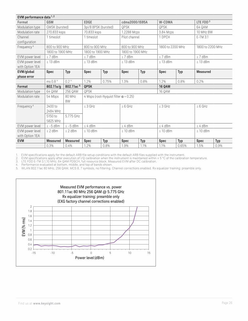
1. EVM specifications apply for the default ARB file setup conditions with the default ARB files supplied with the instrument.2. EVM specifications apply after execution of I/Q calibration when the instrument is maintained within ± 5 °C of the calibration temperature.3. LTE FDD E-TM 3.1,10 MHz, 64 QAM PDSCH, full resource block. Measured EVM after DC calibration.4. Performance evaluated at bottom, middle, and top of bands shown.5. WLAN 802.11ac 80 MHz, 256 QAM, MCS 8, 7 symbols, no filtering. Channel corrections enabled. Rx equalizer training: preamble only.
0.2
0.4
0.6
0.8
1
1.2
1.4
1.6
1.8
2
-15 -10 -5 0 5 10 15
EVM
(% rm
s)
Power level (dBm)
Measured EVM performance vs. power801.11ac 80 MHz 256 QAM @ 5.775 GHz
Rx equalizer training: preamble only(EXG factory channel corrections enabled)

Page 27Find us at www.keysight.com
0
0.2
0.4
0.6
0.8
1
1.2
1.4
1.6
1.8
2
0 2000 3000 4000 5000 60001000
EV
M (
% r
ms)
Frequency (MHz)
Measured EVM performance vs carrier frequency(QPSK, Alpha-0.25, Power = +4 dBm, Symbol Rate = 4 MSyb/s, ALC ON)
0.1
0.2
0.3
0.4
0.5
0.6
0.7
0.8
0.9
1
-10 -5 0 5 10 15
EV
M (
% r
ms)
Power (dBm)
Measured LTE E-TM 3.1 10 MHZ EVM(@ 2100 MHz)with Option 1EA
0
1
2
3
4
5
6
7
8
9
0 2000 3000 4000 5000 60001000
EV
M (
% m
s)
Frequency (MHz)
Measured EVM performance vs carrier frequency(Internal channel correction OFF and ON)
QPSK, Alpha = 0.25, Power = +4 dBm, Symbol rate = 62.5 MSym/s, ALC ON
Correction ONCorrection OFF
0
0.5
1
1.5
2
3
2.5
3.5
4
4.5
5
0 3020 5040 60 7010
EV
M (
% r
ms)
Symbol rate (MHz)
Measured EVM performance vs symbol rate(EXG factory channel correction OFF/ON, ALC ON/OFF)QPSK, Alpha = 0.25, Power = +4 dBm, Freq. = 2.2 GHz
ALC ON-Corrections OFFALC ON-Corrections ONALC OFF-Corrections ON
Bit error rate [BER] analyzer (Option UN7)Clock rate 100 Hz to 60 MHz (usable to 90 MHz)Data patterns PN9, 11, 15, 20, 23Resolution 10 digitsBit sequence length 100 bits to 4,294 Gbits after synchronizationOther features Input clock phase adjustment and gate delay
Direct measurement triggeringData and reference signal outputsReal-time displayBit countError-bit-countBit error ratePass/fail indicationValid data and clock detectionAutomatic re-synchronizationSpecial pattern ignore
Page 28Find us at www.keysight.com
General Specifications
Remote programmingInterfaces GPIB IEEE-488.2, 1987 with listen and talk
LAN 1000BaseT LAN interface, LXI Class C compliantUSB Version 2.0
Control languages SCPI Version 1997.0Compatibility languages Keysight Technologies: N5181A\61A, N 5182A\62A, N5183A, E4438C, E4428C, E442xB, E443xB,
E8241A, E8244A, E8251A, E8254A, E8247C, E8257C/D, E8267C/D, 8648 Series, 8656B, E8663B, 8657A/B, 8662A, 8663AAeroflex Inc.: 3410 SeriesRohde & Schwarz: SMB100A, SMBV100A, SMU200A, SMJ100A, SMATE200A, SMIQ, SML, SMV
Power requirements – 100 to 120 VAC, 50/60/400 Hz – 220 to 240 VAC, 50/60 Hz – 160 W maximum (N5171B) – 300 W maximum (N5172B)
Operating temperature range0 to 55 °CStorage temperature range–40 to 70 °COperating and storage altitudeUp to 15,000 feetHumidityMaximum Relative Humidity (non-condensing): 95%RH up to 40°C, decreases linearly to 45%RH at 55°C.1
Environmental stressSamples of this product have been type tested in accordance with the Keysight Environmental Test Manual and verified to be robust against the environmental stresses of storage, transportation and end-use; those stresses include but are not limited to temperature, humidity, shock, vibration, altitude, and power line conditions; test methods are aligned with IEC 60068-2 and levels are similar to MIL-PRF-28800F Class 3SafetyComplies with European Low Voltage Directive 2006/95/EC
– IEC/EN 61010-1, 2nd Edition – Canada: CSA C22.2 No. 61010-1 – USA: UL std no. 61010-1, 2nd Edition – German Acoustic statement
Acoustic noise emissionLpA < 70 dBOperator positionNormal positionPer ISO 7779
GeraeuschemissionLpA < 70 dBAm ArbeitsplatzNormaler BetriebNach DIN 45635 t.19
EMCComplies with European EMC Directive 2004/108/EC
– IEC/EN 61326-1 or IEC/EN 61326-2-1 – CISPR Pub 11 Group 1, class A – AS/NZS CISPR 11 – ICES/NMB-001
This ISM device complies with Canadian ICES-001; cet appareil ISM est conforme a la norme NMB-001 du Canada
1. From 40 °C to 55 °C, the maximum % Relative Humidity follows the line of constant dew point.
Page 29Find us at www.keysight.com
Memory – Memory is shared by instrument states, user data files, sweep list files, waveform sequences, and other files – 3 GB (30 GB with Option 009) memory available in the N5172B – Security Option 006 allows storage of up to 8 GB on SD card – Depending on how the memory is utilized, a maximum of 1000 instrument states can be saved
No internal non-volatile memory (Option SD0) – Disable/remove any internal non-volatile memory or solid state drive – User will not be able to store any files in the internal memory of the instrument – Not compatible with instrument hardware option 009 (Internal Solid State Memory) and option 660 (Base Band Generator with Real-Time Capability) – Requires firmware B.01.80 or newer
Security (Option 006) – Removable 8 GB solid state memory (SD card) from rear panel – User can force all files to be stored only on external memory card including instrument states, user data files, sweep list files, waveforms, waveform
sequences, and other files – Memory sanitizing, memory sanitizing on, power on, and display blanking – Note: Read/write speeds to external memory card will be slower compared to internal solid-state drive (Option 009)
Self-testInternal diagnostic routines test most modules in a preset condition; for each module, if its node voltages are within acceptable limits, the module passes the testWeight
– N5171B: ≤ 13.6 kg (30 lb) net, ≤ 28.6 kg (63 lb) shipping – N5172B: ≤ 15.9 kg (35 lb) net, ≤ 30.8 kg (68 lb) shipping
Dimensions – 88 mm H x 426 mm W x 489 mm L (length includes rear panel feet) – (3.5 in H x 16.8 in W x 19.2 in L) – Max length (L) including RF connector tip to end of rear panel feet is 508 mm (20 in)
Recommended calibration cycle36 monthsISO compliantThis instrument is manufactured in an ISO-9001 registered facility in concurrence with Keysight Technologies’ commitment to quality.
Inputs and Outputs
Front panel connectorsRF output Outputs the RF signal via a precision N type female connector; see output section for reverse power
protection informationI and Q inputs BNC input accepts “in-phase” and “quadrature” input signals for I/Q modulation; nominal input
impedance is 50 Ω, damage levels are 1 Vrms and 5 VpeakUSB 2.0 Used with a memory stick for transferring instrument states, licenses and other files into or out of the
instrument; also used with U2000, U848X, and U202X Series USB power sensorsRear panel connectorsRear panel inputs and outputs are 3.3 V CMOS, unless indicated otherwise; CMOS inputs will accept 5 V CMOS, 3 V CMOS, or TTL voltage levelsRF output (Option 1EM) Outputs the RF signal via a precision N type female connectorI and Q inputs (Option 1EM) Accepts “in-phase” and “quadrature” input signals for I/Q modulation SMB connector, nominal input
impedance is 50 Ω; damage levels are 1 Vrms and 5 Vpeak; Option 1EM units will come with 2 SMB to BNC adapters
I and Q outputs BNC outputs the analog I/Q modulation signals from the internal baseband generator; nominal output impedance 50 Ω, DC coupled; damage levels ± 2 V
I bar and Q bar outputs (Option 1EL) BNC outputs the complement of the I and Q signals for differential applications;

Page 30Find us at www.keysight.com
Event 1 This connector outputs the programmable timing signal generated by marker 1The marker signal can also be routed internally to control the RF blanking and ALC hold functions; this signal is also available on the AUX I/O connectorWith bit error rate analyzer (Option UN7) this connector is used for data inputDamage levels are > +8 V and < –4 V
Pattern trigger Accepts signal to trigger internal pattern generator to start single pattern output, for use with the internal baseband generatorsAccepts CMOS signal with minimum pulse width of 10 nsFemale BNCDamage levels are > +8 V and < –4 V
BBTRIG 1 For arbitrary and real-time baseband generators I/O such as Markers or trigger inputsWith bit error rate analyzer (Option UN7) this connector is used for clock input
BBTRIG 2 For arbitrary and real-time baseband generators I/O such as Markers or trigger inputsWith bit error rate analyzer (Option UN7) this connector is used for gate input
Sweep out Generates output voltage, 0 to +10 V when the signal generator is sweeping; this output can also be programmed to indicate when the source is settled or output pulse video and is TTL and CMOS compatible in this mode; output impedance < 1 Ω, can drive 2 kΩ; damage levels are ± 15 V
Ext 1 External AM/FM/PM #1 input; nominal input impedance is 50 Ω/600 Ω/1M Ω, nominal; damage levels are ± 5 V
Ext 2 External AM/FM/PM #2 input; nominal input impedance is 50 Ω/600 Ω /1M Ω, nominal; damage levels are ± 5 V
LF OUT 0 to 5 V peak into 50 Ω, –5 V to 5 V offset, nominalPulse External pulse modulation input; this input is TTL and CMOS compatible; low logic levels are 0 V and high
logic levels are +1 V; nominal input impedance is 50 Ω; input damage levels are ≤ –0.3 V and ≥ +5.3 VTrigger in Accepts TTL and CMOS level signals for triggering point-to-point in sweep mode; damage levels are
≤ –0.3 V and ≥ +5.3 VTrigger out Outputs a TTL and CMOS compatible level signal for use with sweep mode
The signal is high at start of dwell, or when waiting for point trigger in manual sweep mode, and low when dwell is over or point trigger is receivedThis output can also be programmed to indicate when the source is settled, pulse synchronization, or pulse videoNominal output impedance 50 ΩInput damage levels are ≤ –0.3 V and ≥ +5.3 V
Reference input Accepts a 10 MHz reference signal used to frequency lock the internal timebase; Option 1ER adds the capability to lock to a frequency from 1 MHz to 50 MHz; nominal input level –3 to +20 dBm, impedance 50 Ω, sine or square waveform
10 MHz out Outputs the 10 MHz reference signal used by internal timebase; level nominally +3.9 dBm; nominal output impedance 50 Ω; input damage level is +16 dBm
LO in (Option 012) Accepts a signal from a master signal generator that is used as the LO for EXG vector in order to configure a phase coherent system; nominal input levels between 0 to +12 dBm; nominal input impedance 50 Ω
LO out (Option 012) Outputs a reference signal that can be used in a phase coherent system; nominal output levels between 0 to +12 dBm; nominal output impedance 50 Ω
DAC Clk In (Option 012) Reserved for future useDigital bus I/O To be used with PXB or N5102A digital signal interface module

This information is subject to change without notice. © Keysight Technologies, 2018 - 2020, Published in USA, February 28, 2020, 5991-0039EN
Page 31Find us at www.keysight.com
Learn more at: www.keysight.comFor more information on Keysight Technologies’ products, applications or services,
please contact your local Keysight office. The complete list is available at:
www.keysight.com/find/contactus
Aux I/O Aux I/O port sends and/or receives auxiliary signaling information:For Option UN7 this connector is used to output reference data, clock, error signals, and moreOutput markers to an external device from arbitrary waveform or real-time generation application such as: frame markers, pulse-per-second, even-second, and more.Input signals from external DUT to modify characteristics of a signal being generated. Such as: changing output power (power control loop testing), advancing or delaying timing (timing advance loop testing), HARQ ACK/NAK delivery (HARQ process loop testing) or streaming external data, clock and symbol synch for custom modulation.I/O is application specific (CDMA, 3GPP, GNSS, LTE, custom etc). See User Guide or Signal Studio help for more details.Connector type: 36 pin 3M connector (part number N10236-52B2PC). The mating connector is a 3M 10136-3000 wire mount plug or 3M 10136-8000 IDC plug with a 3M 10336 shell.
For Option 431 real-time custom modulation the follow pin numbers are assigned:Data input = pin 23Data clock input = pin 29Symbol sync input = pin 25Burst input = pin 27Data output = pin 35Data clock output = pin 6Symbol sync output = pin 37Event 1 output = pin 1Event 2 output = pin 33
USB 2.0 The USB connector provides remote programming functions via SCPILAN (1000 BaseT) The LAN connector provides the same SCPI remote programming functionality as the GPIB connector and is also used to
access the internal Web server and FTP serverSupports DHCP, sockets SCPI, VXI-11 SCPI, connection monitoring, dynamic hostname services, TCP keep aliveLXI class C compliantTrigger response time for the immediate LAN trigger is 0.5 ms (minimum), 4 ms (maximum), 2 ms, typical; delayed/alarm trigger is unknownTrigger output response time is 0.5 ms (minimum), 4 ms (maximum), 2 ms, typical
GPIB The GPIB connector provides remote programming functionality via SCPI
Related Literature
Keysight X-Series Signal Generators
Publication title Publication numberEXG X-Series Signal Generators N5171B Analog & N5172B Vector - Configuration Guide 5990-9958ENMXG X-Series Signal Generators N5181B Analog & N5182B Vector – Data Sheet 5991-0038ENMXG X-Series Signal Generators N5181B Analog and N5182B Vector - Configuration Guide 5990-9959ENKeysight Technologies N5182BX07 Frequency Extender – User’s Guide N5182-90001X-Series RF Signal Generators – Technical Overview 5990-9957ENPathWave Signal Creation - Brochure 5989-6448EN