examples of communication interfaces - chalmerssvenk/mikrodatorsystem/lectures/communicat… · 1...
TRANSCRIPT

1
Examples ofcommunication interfaces
Tranditional interfaces
• No intelligence in the interface
• Only physical connectionOnly physical connection
This could include changes in voltage levels and transformation from ballanced to unballanced signal
• We define the communication protocol in ourapplication programWe might use preprogrammed modules for this
• We have full control of the channel and can usethe interface for our own communication protocolsif we like

2
Modern interfaces
• A high level of intelligence in the interface
• The communication protocol is defined in theinterface
• Much of the control of the communicationchannel is left to the interface and we haveto follow the rules of the communicationstandard to be able to communicate
Here we will focus on the older type of interfaces

3
Parallel link
Unit 1
Unit 2
Serial link
Unit 1
Unit 2

4
Skew in parallel link
Risk of missreading
Unbalanced link
One signal line
Transmitter Reciver
Ground

5
Balanced link
P iti liTransmitter Reciver
Positive line
Negative line
No ground besides maybe shielding
Disturbance on a unbalanced link
The level refered to ground changes
Could give missread signal

6
Disturbance on a balanced link
Both levels change in the same way so the difference is the sameLower risk for missread signal
ModemModulator/demodulator
Telefon modemsTelefon modems
Example V.21
In one direction
’1’ – 980 Hz ’0’ – 1180 Hz
In the other direction
’1’ – 1650 Hz ’0’ – 1850 Hz

7
Parallel interfaces
Two examples
● Memory interface
● GPIB
Memory interface
Example from HC12
Two emulation modes
● Emulation expanded wide
16 bit address bus
16 bit data bus
PORTA and PORTB
PORTA and PORTBMultiplexing
● Emulation expanded narrow
16 bit address bus
8 bit data bus
PORTA and PORTB
PORTAMultiplexing

8
Memory interface cont.External 8K static RAM, 6264
● 13 Address lines → 8K addresses● 13 Address lines → 8K addresses
● 8 Data lines → byte oriented
● Output enable /OE active low
Open for reading
● Write enable /WE active low
Open for writing
● Two chip select signals CS1 and CS2
Activate chip
Memory interface cont.
Two phases
● Address phase
● Data phase
The memory chip still needs to be addressedduring the data phasedu g e da a p ase
Control using external logic

9
Memory interface cont.Control signals from the processor
● Read/write R/W
● E clock ECLK
High for read
Low for write
Low during address phase
High during data phase
Memory interface cont.Address decoding
B dd C000Base address – C000
A15 – A13 = 110
131415131415 AAAAAACS1
10
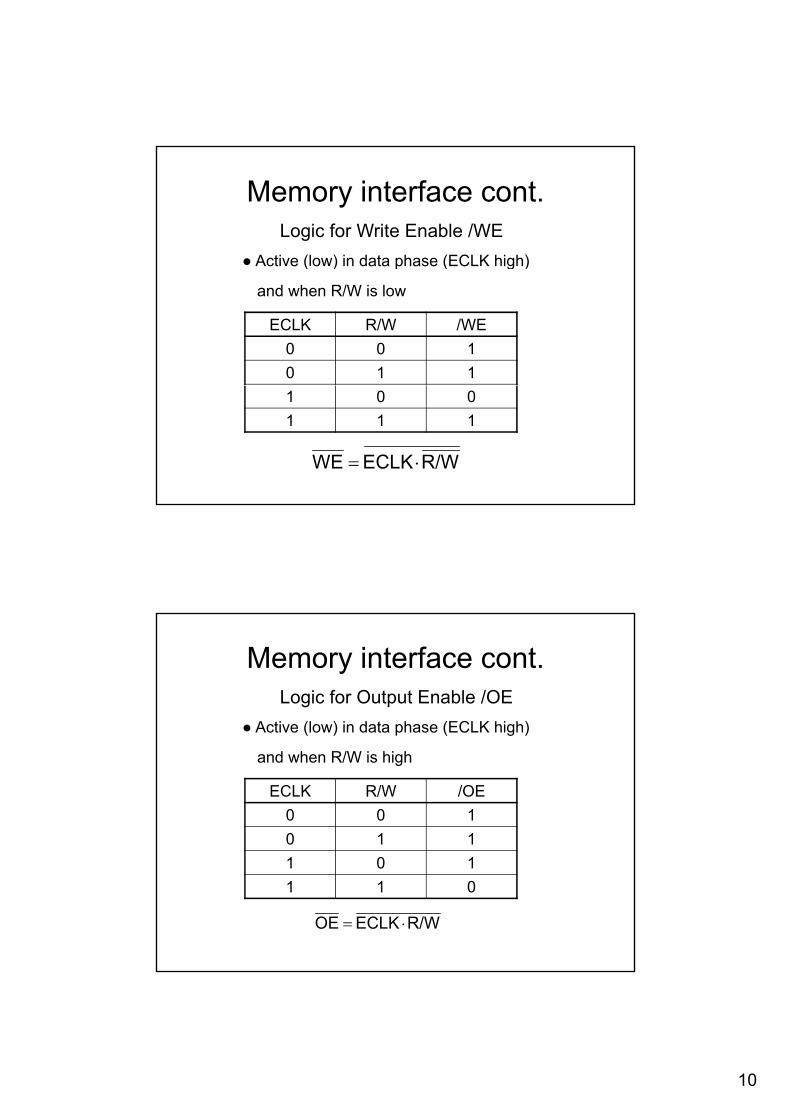
Memory interface cont.Logic for Write Enable /WE
● Active (low) in data phase (ECLK high)Active (low) in data phase (ECLK high)
and when R/W is low
ECLK R/W /WE
0 0 1
0 1 1
1 0 0
1 1 1
R/WECLKWE
Memory interface cont.Logic for Output Enable /OE
● Active (low) in data phase (ECLK high)Active (low) in data phase (ECLK high)
and when R/W is high
ECLK R/W /OE
0 0 1
0 1 1
1 0 1
1 1 0
R/WECLKOE

11
Memory interface cont.6264
A1
A2
A3
A0
D1
D2
D3
D0
Q1
Q2
Q5
Q4
Q3
Q0
Q7
Q6
D1
D2
D5
D4
D3
D0
D7
D6
74HC374
A5
A4
A3
A9
A8
A7
A6
A11
A10
CS1
A12
D5
D4
D3
D7
D6
OE
WE
A15-A8/D7-D0
A12-A8
A15-A13
A7-A0
PO
RT
AP
OR
TB
& &
& &
OE
LECS1
CS2
&
&
&
ECLK
R/W
& &
Discrete logic
Memory interface cont.
PO
RT
AP
OR
TB
Demultiplexer
Can be used for more than one memory area

12
GPIBParallel bus for measurement instruments
General Purpose Instrument Bus
● IEEE-488
● IEEE-488.1 IEC-625
Institute of Electrical and Electronics Engineers
International Electrotechnical Commision
● IEEE-488.2
● SCPI
Standard Commands for Programmable Instruments
GPIB cont.
Up to 15 instruments
Three types of devices
● Controller
● Talker
● Listener
One instrument can have more than one function

13
GPIB cont.
Speed
Standard GPIB up to
1.8 Mbyte/second
High speed GPIB HS488 up tog p p
8 Mbyte/second
GPIB cont.
8 data lines
8 ground lines
3 handshake lines
5 interface management lines

14
GPIB cont.
The handshake lines
NRFD Not Ready for Data
NDAC Not Data Accepted
DAV Data Valid
GPIB cont.
The interface management lines
ATN Attention
EOI End or Identify
IFC Interface Clear
REN Remote Enable
SRQ Service Request

15
GPIB cont.
GPIB cont.Bus configuration
LinearLinear

16
GPIB cont.Bus configuration cont.
StarStar
Device 1 Device 2
Device 4 Device 3
GPIB cont.Bus configuration cont.
Combined linear and starCombined linear and star
Device 1 Device 2Device 5
Device 4 Device 3Device 6

17
GPIB cont.
Connector
Stackable
RS-232-CUnbalanced
Synchronious or asynchronious
Logic one ~ -12 Volts
Logic zero ~ +12 Volts
Synchronious or asynchronious
Up to 20 Kbps in standard but used for higher bit rates, for example 115,2 Kbps
Distances up to 15 meter

18
RS-232-C signals 25 pin DSUB
RS-232-C signals 9 pin DSUB
SCI – Asynchronous Communication Interface

19
Connecting a DTE unit to a DTE unit
DTE1 DTE2Pin Abbriviation Pin Abbriviation1 DCD 1 DCD2 RD 3 TD3 TD 2 RD4 DTR 6 DSR5 SG 5 SG6 DSR 4 DTR7 RTS 8 CTS8 CTS 7 RTS9 RI RI
Zero modem
Pin Output Pin Input4 DTR 1 DCD
6 DSR7 RTS 8 CTS

20
Simplified connection
Sometimes only Rx and Tx are implemented
This could be done
straight In this case the RD and TD connections must be reversed in one end.In most cases at the DCE
Reversed function
DTE DCE
Reversed function
Simplified connection
Sometimes only Rx and Tx are implemented
This could also be done
crossed-over
This type of connection is necessary when two master units are connected together
Make sure that you use the correct type of cable

21
Transfer of the letter ’A’ (6510=4116) odd parity
Odd number of onesStart with LSB
Idle
Startbit
1 0 0 0 0 0 01
Stopb
itData
+12V
+5V
Paritybit
+12V
-12V
RS-232
Transfer of the letter ’A’even parity
Even number of ones
St
St
P
tartb
it
topbit
aritybit
22
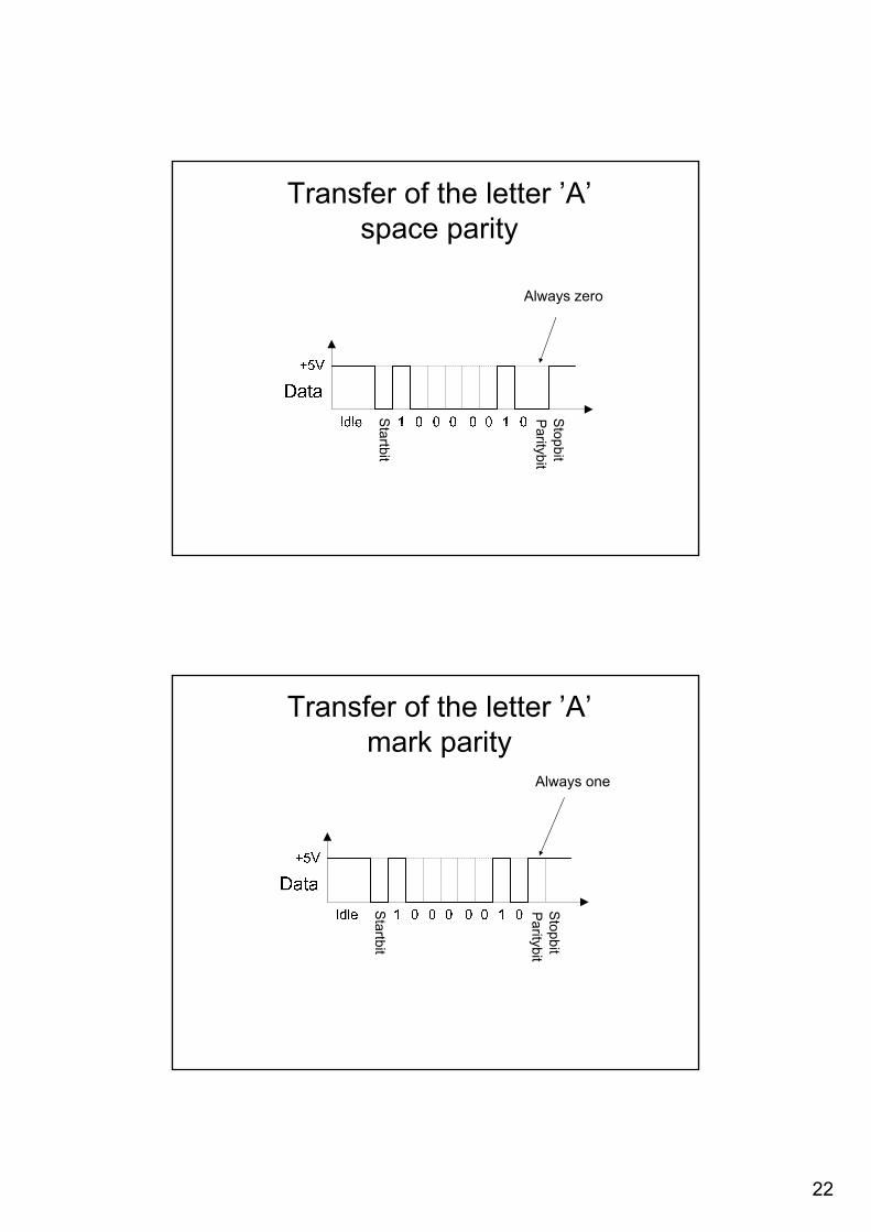
Transfer of the letter ’A’space parity
Al
S SP
Always zero
Sta
rtbit
Stopbit
Paritybit
Transfer of the letter ’A’mark parity
Always one
Start
Sto
pP
arittb
it
pbit
tybit

23
Transfer of the letter ’A’no parity
N it bit
Idle 1 0 0 0 0 0 01
Data
+5V
No parity bit
Typical asynchronoustransmitter
Transmission interrupt request transaction
Data shifted out
Parallel transfer

24
Typical asynchronousreceiver
Reception interrupt request transaction
D t hift d iData shifted in
Parallel transfer
Baud rate and symbol rate
Baud rate is the number of signal changes per second
Symbol rate is the number of symbols per second
In simple transmission the two are the same
In modern transmission techniques (modulation) more thanone symbol can be sent in each bit so the symbol rate might be higher than the baud rate

25
Hamming codingExample
4 data bits
3 parity bits
D3D2D1P2D0P1P0
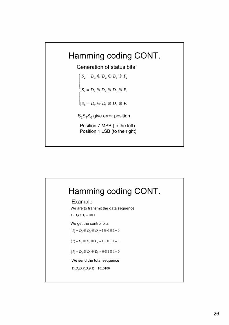
Hamming coding CONT.
Generation of parity bits
0120
0231
1232
DDDP
DDDP
DDDP
exclusive-OR
26
Hamming coding CONT.Generation of status bits
21232 PDDDS
00120
10231
21232
PDDDS
PDDDS
PDDDS
S2S1S0 give error position
Position 7 MSB (to the left)Position 1 LSB (to the right)
Hamming coding CONT.Example
We are to transmit the data sequence
10110123 DDDD
We get the control bits
0101
0101
0231
1232
DDDP
DDDP
01100120 DDDP
We send the total sequence
10101000102123 PPDPDDD

27
Hamming coding CONT.Example cont.
In the receiver we decode the check bits
00110
00101
00101
00120
10231
21232
PDDDS
PDDDS
PDDDS
The result
indicates that the transfer is correct
000012 SSS
Hamming coding CONT.Example cont.
Say that there is a transmission error in bit D1 and we receive the incorrect sequence
10001000102123 PPDPDDD
We decode the check bits
10100
00101
10001
10231
21232
PDDDS
PDDDS
PDDDS
1010000120 PDDDS
10012 5101SSS
indicates an error in bit 5 counted from the right, that is in D1
We can indicate and correct errors in both data and parity bits
but only one bit error

28
RS-422, RS-423 and RS-485
RS-423 unbalanced, faster than RS-232but signal compatible half duplexbut signal compatible, half duplex
RS-422 balanced version of RS-423, half duplex
RS-485, balanced, multi master
Return to zero protocols
’1’ – high duty rate’0’ – low duty rate
Synchronisation

29
Return to zero protocols cont.’0’ – negative pulse’1’ – positive pulse
Synchronisation
Serial peripheral interface, SPISynchronious
Separate clock line
Separate transfer lines in the two directions
Master and slave(s)
Separate clock line
Bit rate up to tens of Mbps
Peripherals at short distance

30
Serial peripheral interface, SPIone slave
From master to slave From slave to master
Master
Slaver e
Serial clock Slave select
Serial peripheral interface, SPI

31
Serial peripheral interface, SPImultiple slaves
S
Master
Slave 2
lave 1
Slave 3
Separate Slave selects
Serial peripheral interface, SPIclocking conditions

32
Serial peripheral interface, SPIclocking conditions cont.
CPHA=0
Serial peripheral interface, SPIclocking conditions cont.
CPHA=1
SCLK
SCLK
CPOL=0
CPOL=1
Present bit
Sample bit
MOSI
MISO
SS
33
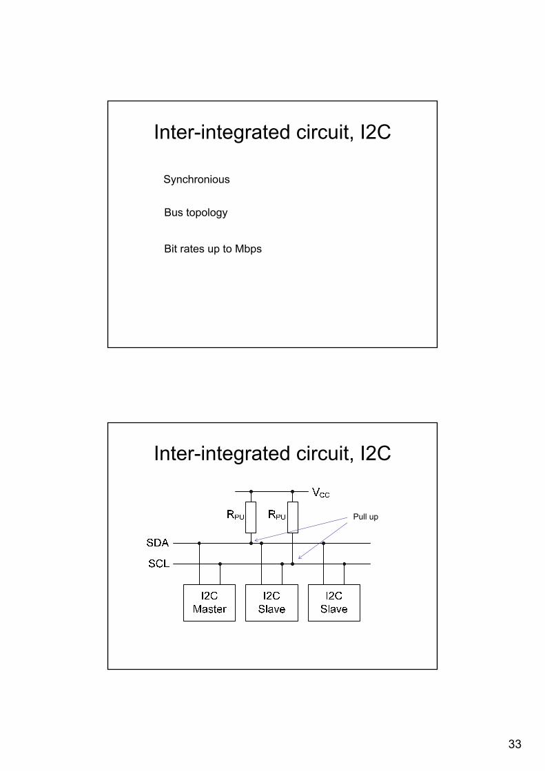
Inter-integrated circuit, I2C
Synchroniousy
Bus topology
Bit rates up to Mbps
Inter-integrated circuit, I2C
Pull up

34
Inter-integrated circuit, I2C cont.
VCC
RPU RPU
SDA
SCL
CLK1OUT
Data1OUT
Data2OUT
CLK2OUT
CLK1IN
Data1IN
Device1 Device2
Data2IN
CLK2IN
Inter-integrated circuit, I2C cont.
Master transmitting two bytes of data to slave
S Slave address A Data A DataR/W A/A P
’0' write
From master to slave
From slave to master
R/W = read/write
A = acknowledge
S = start condition
P = stop condition
A = not acknowledgeg

35
Inter-integrated circuit, I2C cont.
Master receiving two bytes of data from slave
Inter-integrated circuit, I2C cont.
Start condition

36
Inter-integrated circuit, I2C cont.
Stop condition
Inter-integrated circuit, I2C cont.
ACK condition

37
Inter-integrated circuit, I2C cont.
NACK condition
Inter-integrated circuit, I2C cont.
Bit transaction
SDA
SCL
Bit transaction
Data valid

38
1-wire bus
Dallas Semiconductor
Bus and ground
• Bus interface
Twisted pair
• One master and slaves
Power supply through the bus
1-wire bus
Structure
Pull up

39
1-wire busSignaling
B hi h h idlBus high when idle
Reset (from master)
Bus low more than 480 µseconds
1-wire busBit transfer
Start of bit transfer
Master pulls bus low for a short while
Sending node (master or slave)
’1’ keeps the bus low for more than 60 µseconds
Start of bit transfer
1 keeps the bus low for more than 60 µseconds
’0’ keeps the bus low for less than 15 µseconds
Bits are transmitted LSB first
40
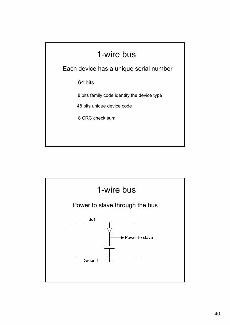
1-wire bus
Each device has a unique serial number
64 bits
8 bits family code identify the device type
48 bits unique device code
8 CRC check sum
1-wire bus
Power to slave through the bus

41
1-wire bus
Power to slave through the bus cont.
Capacitor charged when bus is highCapacitor charged when bus is high
Capacitor isolated from bus when bus is low
Capacitor supplies the power