evaluation of microcontroller based packet radio modem
TRANSCRIPT

Evaluation of Microcontroller Based Packet Radio Modem
Phillip Sello Seabe
Thesis presented in partial fulfilment of the requirements for the degree of Master of Science
in Engineering Sciences at the University of Stellenbosch
SUPERVISOR: Prof. S Mostert
March 2007

Declaration
I, the undersigned, hereby declare that the work contained in this thesis is my own original work
and that I have not previously in its entirety or in part submitted it at any university for a degree.
Signature: ........................................ Date: ...................................

Abstract
The use of emerging microprocessors has become increasingly popular in packet radio commu-
nication equipment. This is mainly because of the improved performance and hardware sim-
plicity they offer. The new generation field programmable gate arrays (FPGAs) and microcon-
trollers are now widely used in the development of terminal node controller (TNC) components.
The aim of this thesis is to evaluate the use of these new generation FPGAs and microcon-
trollers in a TNC design, in order to utilise the software flexibility and hardware simplicity. The
design process began with the selection of the available simple microcontroller-based modem
that was just designed. Prior to its usage in a TNC, the software of the modem was modelled,
in order to understand its signal processing functionality.

Opsomming
Kleiner mikroverwerkers word meer en meer gebruik in pakket radio kommunikasie toerusting,
meerendeels te danke aan hul hoe werkverrigting en hardeware eenvoud. Nuwe generasie
FPGAs en mikroverwerkers word wyd gebruik in die ontwikkeling van kommunikasie terminaal
beheerders (TNC).
Die doel van die verslag is om die aanwending van hierdie nuwe generasie FPGAs en mikrover-
werkers in ’n TNC te evalueer. Die ontwerpsproses het afgeskop met die keuse van ’n beskik-
bare en eenvoudige mikroverwerker gebasseerde modem. Om die modem se sein verwerking
te verstaan, is die modem se sagteware eers gemodelleer. Daarna is ’n UART, HDLC beheerder
en kommunikasie beheer verwerker in ’n FPGA ontwerp en getoets. Ten slotte is die oplossing
van die projek vergelyk met soortgelyke kommunikasie terminaal beheerders.

Contents
1 Introduction 11.1 The History of Packet Radio . . . . . . . . . . . . . . . . . . . . . . . . . . . 1
1.2 Previous Solutions . . . . . . . . . . . . . . . . . . . . . . . . . . . . . . . . 2
1.3 What is the Solution . . . . . . . . . . . . . . . . . . . . . . . . . . . . . . . . 2
1.4 Why the Solution is Better . . . . . . . . . . . . . . . . . . . . . . . . . . . . 2
1.5 Document Outline . . . . . . . . . . . . . . . . . . . . . . . . . . . . . . . . . 3
2 Preliminary Studies 42.1 Introduction . . . . . . . . . . . . . . . . . . . . . . . . . . . . . . . . . . . . 4
2.2 TNC Components . . . . . . . . . . . . . . . . . . . . . . . . . . . . . . . . 5
2.2.1 PC Communication Interface . . . . . . . . . . . . . . . . . . . . . . . 5
2.2.2 Memory Interface Controllers . . . . . . . . . . . . . . . . . . . . . . 7
2.2.3 FIFO Memory . . . . . . . . . . . . . . . . . . . . . . . . . . . . . . 7
2.2.4 HDLC Controller . . . . . . . . . . . . . . . . . . . . . . . . . . . . . 8
2.2.5 Packet Radio Modem . . . . . . . . . . . . . . . . . . . . . . . . . . . 9
2.3 Summary . . . . . . . . . . . . . . . . . . . . . . . . . . . . . . . . . . . . . 12
3 The 9600 Baud Packet Radio Modem 133.1 Introduction . . . . . . . . . . . . . . . . . . . . . . . . . . . . . . . . . . . . 13
3.2 Transmitter . . . . . . . . . . . . . . . . . . . . . . . . . . . . . . . . . . . . 13
3.2.1 Randomiser . . . . . . . . . . . . . . . . . . . . . . . . . . . . . . . . 13
3.2.2 Finite Impulse Response Filter (FIR) . . . . . . . . . . . . . . . . . . 14
3.3 Receiver . . . . . . . . . . . . . . . . . . . . . . . . . . . . . . . . . . . . . . 14
3.3.1 Clock Recovery . . . . . . . . . . . . . . . . . . . . . . . . . . . . . . 14
3.3.2 Data Carrier Detect . . . . . . . . . . . . . . . . . . . . . . . . . . . . 15
3.3.3 Unscrambler . . . . . . . . . . . . . . . . . . . . . . . . . . . . . . . 15
3.4 Summary . . . . . . . . . . . . . . . . . . . . . . . . . . . . . . . . . . . . . 16
i

4 The G4XYW Modem 174.1 Introduction . . . . . . . . . . . . . . . . . . . . . . . . . . . . . . . . . . . . 17
4.2 G4XYW Modem Analysis . . . . . . . . . . . . . . . . . . . . . . . . . . . . 18
4.2.1 G4XYW TX Mode . . . . . . . . . . . . . . . . . . . . . . . . . . . . 18
4.2.2 G4XYW RX Mode . . . . . . . . . . . . . . . . . . . . . . . . . . . . 21
4.3 G4XYW Execution Times . . . . . . . . . . . . . . . . . . . . . . . . . . . . 25
4.3.1 TX Timer Interrupt Routine . . . . . . . . . . . . . . . . . . . . . . . 26
4.3.2 Scrambling Time . . . . . . . . . . . . . . . . . . . . . . . . . . . . . 26
4.3.3 Clock Recovery Time . . . . . . . . . . . . . . . . . . . . . . . . . . 26
4.3.4 Comparator Interrupt Time . . . . . . . . . . . . . . . . . . . . . . . . 27
4.3.5 Descrambler Execution Time . . . . . . . . . . . . . . . . . . . . . . . 28
4.3.6 Total Execution Time . . . . . . . . . . . . . . . . . . . . . . . . . . . 28
4.4 Microcontroller Program Memory Usage . . . . . . . . . . . . . . . . . . . . 29
4.5 The G4XYW Modem Characteristics . . . . . . . . . . . . . . . . . . . . . . 30
4.6 Summary . . . . . . . . . . . . . . . . . . . . . . . . . . . . . . . . . . . . . 30
5 G4XYW Modem Simulation 325.1 Introduction . . . . . . . . . . . . . . . . . . . . . . . . . . . . . . . . . . . . 32
5.2 Modulation . . . . . . . . . . . . . . . . . . . . . . . . . . . . . . . . . . . . 32
5.3 Demodulation . . . . . . . . . . . . . . . . . . . . . . . . . . . . . . . . . . . 35
5.4 Conclusion . . . . . . . . . . . . . . . . . . . . . . . . . . . . . . . . . . . . 36
6 HDLC Controller Design 376.1 Introduction . . . . . . . . . . . . . . . . . . . . . . . . . . . . . . . . . . . . 37
6.2 PC Interface (UART) . . . . . . . . . . . . . . . . . . . . . . . . . . . . . . . 38
6.3 HDLC Controller . . . . . . . . . . . . . . . . . . . . . . . . . . . . . . . . . 39
6.4 Memory Interface Controller . . . . . . . . . . . . . . . . . . . . . . . . . . . 41
6.5 Simulation Results . . . . . . . . . . . . . . . . . . . . . . . . . . . . . . . . 43
6.6 VHDL Compilation Report . . . . . . . . . . . . . . . . . . . . . . . . . . . . 44
6.7 Conclusion . . . . . . . . . . . . . . . . . . . . . . . . . . . . . . . . . . . . 44
7 Results and Conclusion 457.1 Introduction . . . . . . . . . . . . . . . . . . . . . . . . . . . . . . . . . . . . 45
7.2 Implemented System . . . . . . . . . . . . . . . . . . . . . . . . . . . . . . . 45
7.3 Functional Results of the Whole System . . . . . . . . . . . . . . . . . . . . . 46
7.3.1 Frame Check Sequence Field . . . . . . . . . . . . . . . . . . . . . . . 48
ii

7.3.2 Bit Stuffing . . . . . . . . . . . . . . . . . . . . . . . . . . . . . . . . 49
7.4 Performance . . . . . . . . . . . . . . . . . . . . . . . . . . . . . . . . . . . . 50
7.4.1 FPGA Performance . . . . . . . . . . . . . . . . . . . . . . . . . . . . 50
7.4.2 SRAM Performance . . . . . . . . . . . . . . . . . . . . . . . . . . . 51
7.5 Modem Comparisons . . . . . . . . . . . . . . . . . . . . . . . . . . . . . . . 51
7.6 Conclusion . . . . . . . . . . . . . . . . . . . . . . . . . . . . . . . . . . . . 55
7.7 Recommendations . . . . . . . . . . . . . . . . . . . . . . . . . . . . . . . . . 56
A HDLC VHDL Code 57
B The G4XYW MATLAB Simulation Code 126
C G4XYW Modem Source Code 133
D G4XYW Modem Circuit 167
E The G3RUH Schematic Diagram 169
F Tools used for the Project 172F.1 Hardware . . . . . . . . . . . . . . . . . . . . . . . . . . . . . . . . . . . . . 172
F.2 Software . . . . . . . . . . . . . . . . . . . . . . . . . . . . . . . . . . . . . . 173
iii

List of Figures
2.1 TNC Functional Block Diagram . . . . . . . . . . . . . . . . . . . . . . . . . 4
2.2 RS232 Character Format . . . . . . . . . . . . . . . . . . . . . . . . . . . . . 6
2.3 Effect of Timing Error . . . . . . . . . . . . . . . . . . . . . . . . . . . . . . 6
2.4 HDLC Frame Format . . . . . . . . . . . . . . . . . . . . . . . . . . . . . . . 8
2.5 The G3RUH Circuit Board [14] . . . . . . . . . . . . . . . . . . . . . . . . . 10
2.6 The YAM Modem Circuit Board [9] . . . . . . . . . . . . . . . . . . . . . . . 11
3.1 The Shift Register Scrambler Implementation . . . . . . . . . . . . . . . . . . 14
3.2 Shift Register Unscrambler Implementation . . . . . . . . . . . . . . . . . . . 15
4.1 The G4XYW Circuit Board . . . . . . . . . . . . . . . . . . . . . . . . . . . . 17
4.2 Block Diagram of G4XYW Modem . . . . . . . . . . . . . . . . . . . . . . . 18
4.3 G4XYW TX Main Loop Flow Diagram . . . . . . . . . . . . . . . . . . . . . 20
4.4 G4XYW Digital Phase Lock Loop . . . . . . . . . . . . . . . . . . . . . . . . 22
4.5 TX Timer Interrupt Execution Time . . . . . . . . . . . . . . . . . . . . . . . 26
4.6 Scrambler Execution Time . . . . . . . . . . . . . . . . . . . . . . . . . . . . 27
4.7 Analog Comparator Interrupt Routine Execution Time . . . . . . . . . . . . . 28
4.8 Unscrambler Execution Time . . . . . . . . . . . . . . . . . . . . . . . . . . . 28
5.1 TX Input Data (TXD) . . . . . . . . . . . . . . . . . . . . . . . . . . . . . . . 33
5.2 Scrambled Data . . . . . . . . . . . . . . . . . . . . . . . . . . . . . . . . . . 33
5.3 Scrambler Output Calculation . . . . . . . . . . . . . . . . . . . . . . . . . . 34
5.4 FIR output . . . . . . . . . . . . . . . . . . . . . . . . . . . . . . . . . . . . . 34
5.5 Comparator Output . . . . . . . . . . . . . . . . . . . . . . . . . . . . . . . . 35
5.6 Demodulator Output . . . . . . . . . . . . . . . . . . . . . . . . . . . . . . . 35
6.1 FPGA block diagram . . . . . . . . . . . . . . . . . . . . . . . . . . . . . . . 38
6.2 Transmit Module Block Diagram . . . . . . . . . . . . . . . . . . . . . . . . . 39
6.3 CRC Architecture to Implement Polynomial X16 + X15 + X2 + 1 . . . . . . . . 40
iv

6.4 Receive Module Block Diagram . . . . . . . . . . . . . . . . . . . . . . . . . 41
6.5 The HDLC Timing Diagram . . . . . . . . . . . . . . . . . . . . . . . . . . . 43
6.6 FPGA Simulation . . . . . . . . . . . . . . . . . . . . . . . . . . . . . . . . . 43
6.7 The VHDL Compilation Report Summary . . . . . . . . . . . . . . . . . . . . 44
7.1 TNC Components Block Diagram . . . . . . . . . . . . . . . . . . . . . . . . 46
7.2 Transmission and Reception of Two Characters “UN” . . . . . . . . . . . . . . 47
7.3 Transmitted Bitstreams . . . . . . . . . . . . . . . . . . . . . . . . . . . . . . 48
7.4 FCS Shift Register During Characters “UN” Transmission . . . . . . . . . . . 48
7.5 Bit Stuffing . . . . . . . . . . . . . . . . . . . . . . . . . . . . . . . . . . . . 49
7.6 Measured Bit Stuffing Effect . . . . . . . . . . . . . . . . . . . . . . . . . . . 50
7.7 FPGA performance . . . . . . . . . . . . . . . . . . . . . . . . . . . . . . . . 51
7.8 Modem Board Areas in cm2 . . . . . . . . . . . . . . . . . . . . . . . . . . . 52
7.9 Number of Components Per Modem . . . . . . . . . . . . . . . . . . . . . . . 53
7.10 Power Consumption For Each Modem (Watts) . . . . . . . . . . . . . . . . . . 54
D.1 G4XYW circuit-Part1 . . . . . . . . . . . . . . . . . . . . . . . . . . . . . . . 167
D.2 G4XYW circuit-Part2 . . . . . . . . . . . . . . . . . . . . . . . . . . . . . . . 168
E.1 The G3RUH Schematic Diagram - Part1 [8] . . . . . . . . . . . . . . . . . . . 170
E.2 The G3RUH Schematic Diagram - Part2 [8] . . . . . . . . . . . . . . . . . . . 171
v

List of Tables
2.1 Characteristics of RS232, RS422, RS423 and RS485 [7] . . . . . . . . . . . . 5
4.1 Four RX Loop Phases . . . . . . . . . . . . . . . . . . . . . . . . . . . . . . . 23
4.2 G4XYW execution time requirements . . . . . . . . . . . . . . . . . . . . . . 29
4.3 Microprocessor Memory Use Summary[Bytes] . . . . . . . . . . . . . . . . . 30
F.1 FPGA device resources . . . . . . . . . . . . . . . . . . . . . . . . . . . . . . 172
vi

List Of Abbreviations and Acronyms
ADC Analog to Digital Converter
AFSK Audio Frequency Shift Keying
ALU Arithmetic Logic Unit
AMSAT Amateur Satellite Corporation
ASCII American Standard Code For Information Interchange
bps Bits per Second
CMOS Complementary Metal Oxide Semiconductor
CRC Cyclic Redundancy Check
DAC Digital to Analog Converter
DC Direct Current
DCD Data Carrier Detect
DPLL Digital Phase Lock Loop
DSP Digital Signal Processing
EEPROM Electrically Erasable Programmable Read-only Memory
FCS Frame Check Sequence
FIFO First In First Out
FIR Finite Impulse Response Filter
FPGA Field Programmable Gate Arrays
FSK Frequency Shift Keying
GND Ground
HDL Hardware Descriptive Language
HDLC High-Level Data Link Control
I/O Input-Output
IC Integrated Circuit
IF Intermediate Frequency
LED Light Emitting Diode
MHz Mega Hertz
MIPS Million Instructions per Second
NBFM Narrow Band Frequency Modulation
PC Personal Computer
PCB Printed Circuit Board
PTT Push-To-Talk
RAM Random Access Memory
RF Radio Frequency
vii

RX Receiver
SRAM Static Random Access Memory
TAPR Tucson Amateur Packet Radio
TNC Terminal Node Controller
TX Transmitter
UART Universal Asynchronous Receiver and Transmitter
UHF Ultra High Frequency
USB Universal Serial Bus
VHF Very High Frequency
viii

Chapter 1
Introduction
1.1 The History of Packet Radio
Packet radio communications has been used for many years so far. Amateur packet radio began
in Montreal, Canada in 1978, the first transmission occurring on May 31st [17]. This was
followed by Vancouver Amateur Digital communication Group (VADCG) development of a
Terminal Node Controller (TNC) in 1980 [17]. This practice is exercised by many as a hobby
for communicating with other radio amateurs. Since packet radio is not commercial, most of the
enthusiasts have relied on do it yourself principle when coming to communicating equipment.
Since not all people interested in packet radio communications are experienced engineers who
can do things themselves, some organisations started developing packet radio communicating
devices for business. Use of packet communication devices for satellites and ground stations is
for low volumes and very cost sensitive utilisation. Some of the problems about these devices
are:
1. Costs: most of these organisations are based in Europe and America. Though the costs of
the equipment might not be high, the shipping costs are always a worrying factor.
2. Availability: because the developers were not making profit on sales, they often got re-
luctant to manufacture bulks of equipment [5].
3. Obsolete components: though most of the traditional components are still functional,
most of the components that were built with are no longer available. This was verified by
enquiring about some of the components used in G3RUH modem.
4. Complexity: the designs and the usage of the equipment were difficult to follow due to
the number of components that were used to build the circuits.
1

CHAPTER 1. INTRODUCTION 2
5. Power consumption: the components that were used in the old TNC circuits consume
more power than the current ones.
1.2 Previous Solutions
The implementation of the newer packet radio modems was done by replacing the the older ob-
solete components by equally functional available components. The complexity of the modem
designs has been relatively the same over years. To a certain extent, these new components
also reduced the power consumption problem. Though the usage of software has been increas-
ing some developers still could not utilise the simplicity the software, microcontrollers and the
FPGAs offers.
1.3 What is the Solution
The usage of software and evolving low cost FPGAs and microprocessors was utilised to im-
prove the solution. As a starting point a microprocessor based modem that was also to be
evaluated was considered for the project. In addition to the modem employed, the use of a
simple commercial FPGA evaluation board was also investigated and ultimately used. The list
of the tools that were used for this project can be found in Appendix F.
1.4 Why the Solution is Better
The following factors make the solution found in this project to be an improvement over the
previous solutions.
1. Simplicity: the functionality of the system designed in this project are around two pieces
of devices, an FPGA and a relatively small microcontroller.
2. Flexibility: with most of the functional blocks of the system implemented in software, in
some instances the modification of the system properties is as easy as changing the values
of the software code variables.
3. Availability and latency: none of the components and the software were difficult to obtain.
The latency period was short because all of the components were supplied by the local
distributors.

CHAPTER 1. INTRODUCTION 3
4. Power consumption: most of the components manufactured today consume low power
compared to their equally functional old counterparts.
1.5 Document Outline
• Chapter 2 gives some background studies on the TNC functions and its components. A
typical physical diagram of a simple TNC is also illustrated.
• Chapter 3 introduces the fundamentals of the structure and the functionality of the mo-
dem.
• Chapter 4 analyse the G4XYW modem. The modem was chosen because it simple and
affordable. The modem is said to offer the same functionality as the tried and tested
G3RUH modem. However the G4XYW is based on software as compared to the hardware
based G3RUH modem.
• After the analyses of the modem was done in chapter 4, the MATLAB simulation pro-
cedure is presented. The outcome of Chapter 5 was the first achievement in finding the
solution for this project problem. Firstly, the microcontroller or FPGA based modems
had to be evaluated before they could be used.
• Chapter 6 discusses how the whole system was designed. This chapter gives an overview
of how the project problem statement was solved.
• Chapter 7 gives the functional results, summary and the conclusion of the project.

Chapter 2
Preliminary Studies
2.1 Introduction
Terminal Node Controllers (TNC) are used to interface a digital data source, typically a personal
computer (PC) with radio transmitters in the VHF or UHF bands. A TNC is comprised of two
functional parts: a transmitter and a receiver of a data packets. Figure 2.1 depicts a block
diagram of a typical TNC. As a transmitter, a TNC accepts data from a digital source and
PROCESSOR
TX
SRAM
TX
UART controller
RX RX
HDLC Controller
Tx
Rx
TxD
RxD
Analog signal
RxData
TxData Control Signals
Data[0..7]
Data[0..7]
Control Signals
Control signals
Data[0..7]
Control Signal
Data[0..7]
Control signals
Data[0..7]
Packet radio modem
Figure 2.1: TNC Functional Block Diagram
processes it. Before the processing starts, the data is first stored in a memory. The processing of
data involves inserting start and end of file flags, the address of the receiver, bit stuffing and an
error check field on the packet to be transmitted. After the processing is done, a digital bit stream
is then converted into an analog signal. Finally, this analog signal is sent to an RF transmitter.
The receiver of the TNC accepts an analog signal from the RF receiver and transmits a digital
data to a PC. The receiver starts by extracting a clock from the received signal and converting
the signal into a digital bit stream. The receiver synchronises with the incoming data by first
4

CHAPTER 2. PRELIMINARY STUDIES 5
detecting a unique flag pattern. The receiver will then perform error checking on the received
data before sending it to the PC.
2.2 TNC Components
As discussed in section 2.1, a TNC is used to interface a PC and an RF transceiver. This section
discusses the components of the TNC.
2.2.1 PC Communication Interface
There are various communication methods that can be used between two devices. Some are
serial and others are parallel. Parallel communication methods are usually faster than serial
ones. The choice of the communication method for this project was based on the following:
1. The availability of the interface hardware
2. The ability to communicate over an estimated distance between the PC and the TNC
3. The ability to communicate at an required baud rate
4. The ability to communicate in a full duplex mode.
Table 2.1: Characteristics of RS232, RS422, RS423 and RS485 [7]RS232 RS422 RS423 RS485
Differential no yes no yes
Modes of operation full duplex half duplex half duplex half duplex
Network topology point-to-point multi drop multi drop multi point
Maximum distance 15 m 1200 m 1200 m 1200 m
Using Table 2.1 and the factors mentioned above, RS232 was the serial communication method
chosen for the project. Firstly, most PCs have an RS232 interface. A baud rate of up to 20 K
bits per second can be attained with a serial cable of approximately 15 m or less [7].
RS232 Specifications RS232 is an asynchronous serial communication method. The com-
munication is established by sending or receiving data in characters. Each character has at least
a start bit, 5 to 8 data bits, and a stop bit. The length of the stop bit is usually 1, 1.5, or 2 times
the duration of an ordinary bit. In addition to that, an optional parity bit can be added between
the data and stop bits. Figure 2.2 illustrates the character format.

CHAPTER 2. PRELIMINARY STUDIES 6
7 5 6 8 3 4 1 2 Start bit
Stop bit
1
0
data bits
Idle state of line
Remaining idle or next start bit
Figure 2.2: RS232 Character Format
RS232 Timing Procedure The scheme avoids synchronisation problems by avoiding long,
uninterrupted bit streams. The transmitter establishes timing or synchronisation within each
character so that the receiver can resynchronise at the beginning of each new character. As
shown in Figure 2.2, each character has a start bit that can be used by the receiver to synchronise.
When no data is being transmitted, the line between the transmitter and the receiver is in an idle
state. The idle state is a condition whereby a transmission line stays at a logic level different
from that of a start bit.
Error Detection As an option data bits are appended with a parity bit. This bit is used by the
receiver for error detection.
RS232 Disadvantages Even with the start bit synchronisation technique, timing problems
can be experienced if the receiver clock is slower or faster than that of the transmitter. Fig-
ure 2.3 illustrates a timing error resulting from a speed difference between the receiver and the
transmitter. From the figure, the bit period of the transmitter is 100 µs while that of the receiver
is 6 percent faster (94 µs according to transmitter’s clock). As shown in Figure 2.3, the last bit
is not sampled correctly by the receiver. This timing error can also result in a condition called
framing error. The framing error is a condition where the character bit count is out of alignment.
7 5 6 8 3 4 1 2 Start bit
Stop bit
100 200 300 400 500 600 700 800 900 Transmitter timing
Receiver timing 97 191 285 379 473 567 661 755 849
Figure 2.3: Effect of Timing Error
Referring to Figure 2.3, if bit 7 is a 1 and bit 8 is a 0, bit 8 could be mistaken for a start bit. The
general formula for calculating the allowed timing difference between the transmitter and the
receiver is as follows:
n × T f aster > (n − 0.5) × Tslower (2.1)

CHAPTER 2. PRELIMINARY STUDIES 7
where n is the number of bits (5 to 8) per character, T f aster and Tslower are periods of faster and
slower clocks, respectively.
As compared to other serial communication interfaces such as RS485, the RS232 is not immune
to noise. Noise interference can cause problems such as framing error. The other disadvantage
with the asynchronous transmission is the overhead of two to three bits per character. For
example, for an 8-bit character with no parity bit, using a 1-bit-long stop bit, two out of every
ten bits carry no information but are there only for synchronisation purposes. This makes an
overhead of 20 percent.
RS232 Advantages The RS232 standard defines low-cost serial communication in a robust
way where bits are sent sequentially on a conducting line [18]. The other advantage of the
RS232 is that it is a full duplex.
2.2.2 Memory Interface Controllers
The memory interface controller is used to control the writing and reading of data to and from
the memory. This is necessary to avoid memory bus contention. The memory is accessed by
four the TNC components as follows:
• TX UART transmitter unit supplies the memory interface controller with data received
from the PC. This data has to be stored in the memory before the processing can com-
mence.
• After the last character has been written into the memory, the TX HDLC controller fetches
the data from the memory, one character at a time.
• During data reception the RX HDLC controller needs to store the received data into the
memory before the data can be transmitted to the PC. This is performed to control the
data transmission rate which may be different from the reception rate.
• Finally, the RX UART controller fetches data from the memory one character at a time
and transmits it to the PC one bit per time.
2.2.3 FIFO Memory
Before data is transmitted or received, it has to be processed. To avoid data overrun or underrun
from the data source, the TNC buffers bits stream into a FIFO memory before processing begins.
The memory width was chosen to be the same size as the character bit length. The size of the

CHAPTER 2. PRELIMINARY STUDIES 8
memory was chosen to be sufficient to store the intended HDLC frame size. For this project an
8-bit 256KB SRAM device on the development board was used.
2.2.4 HDLC Controller
All TNC transmissions are in the form of HDLC frames. HDLC is a standard protocol in packet
radio. HDLC is a synchronous transmission protocol which overcomes synchronous transmis-
sion problems. An HDLC frame is comprised of a number of fields. The flag, address, and
control fields that precede the information field are known as a header [1]. The last two fields
are the Frame Check Sequence (FCS), and the flag, they are reffered to as a trailer. Figure 2.4
depicts the structure of the HDLC frame.
Control Flag FCS Information
8 or 16 bits Variable 16 or 32 bits
8 bits
Address
8 extendable
Flag
8 bits
Header Trailer
Figure 2.4: HDLC Frame Format
Flag Fields Flag fields delimit the frame at both ends with the unique pattern 01111110. The
receiver synchronises on the start of the frame by continuously searching for the flag pattern.
While receiving the a frame, a TNC continues to hunt for the pattern to determine the end of the
frame. Since there is no restriction on the data source, the transmitter makes sure that no data
containing the bit sequence of the flag is transmitted. The procedure used to accomplish this is
called bit stuffing. Between the transmission of the starting and the ending flags, the transmitter
will always insert an extra 0 bit after each occurrence of five 1s in the frame. From the receiver
side, after detecting the start flag, the bit stream is monitored. When a pattern of five 1s appears,
the sixth bit is examined. If this bit is a 0, it is deleted. If the sixth bit is a 1 and the seventh is
a 0, the combination is considered to be a flag. If the sixth and the seventh bits are both 1, the
sender is indicating an abort condition [1].
Address Field The address field identifies the secondary station that transmitted or is to re-
ceive the frame. This field is not needed for point-to-point links. Hence for this project this field
is not included.

CHAPTER 2. PRELIMINARY STUDIES 9
Control Field There are three types of frames that are defined in the HDLC protocol. Each
of the three frame types has a different control field format. The three frames are information
frames, supervisory frames and unnumbered frames. Information frames carry the data to be
transmitted. In addition to that, the frame has flow and error control data. For this project the
control field was also excluded.
Information Field The information field can contain any sequence of bits but must consist
of an integral number of bytes. The length of the field is variable up to some system-defined
maximum, that is the size of the memory.
Cyclic Redundancy Check (CRC) CRC is one of the common error-detecting codes [1]. It
can be described as follows, given a X-bit block of transmitted bits, the transmitter generates
an Y-bit sequence, known as an FCS. This will result in a frame consisting of X + Y bits which
are divisible by some predetermined number. The receiver divides the incoming frame by that
number. If there is no remainder, receiver assume there was no error.
Frame Check Sequence The frame check sequence (FCS) is an error-detecting code calcu-
lated from the remaining fields except the flag field. The length of the field is normally 16 or
32 bits long. The FCS is generated by CRC. CRC generate an FCS according to a specified
polynomial. The two CRC polynomial that are popular for 8-bit characters, are [1]:
CRC-16 = X16 + X15 + X2 + 1
CRC-CCITT = X16 + X12 + X5 + 1
The two polynomials generate a 16-bit FCS.
2.2.5 Packet Radio Modem
The last TNC component is a packet modem. Briefly, a packet modem is used to convert a
digital data into an analog signal. The conversion is performed for RF modulation purposes. It
is only after modulation is done that VHF transmission can be performed. The following are
some of the well known packet radio modems:
The Bell-202 AFSK modem: When AX.25 protocol amateur packet radio communications
first began in the early 1980s, early experimenters used Bell-202 type Audio Frequency Shift
Keying (AFSK) telephone modems to pass binary packet data over the air using voice-grade
Very High Frequency (VHF) narrowband Frequency Modulation (FM) transceivers [2]. The

CHAPTER 2. PRELIMINARY STUDIES 10
baud rate of the Bell-202 modems was 1200 bits per second. They functioned satisfactorily for
half duplex radio communications. The first terminal controllers to make an appearance on the
commercial market, included the Bell-202 modem [2].
The G3RUH modem: G3RUH, which was designed in 1988, is a full duplex 9600 baud
Frequency Shift Keying (FSK) packet radio modem. The modem was designed for terres-
trial packet and satellite packet applications with typical Narrow Band Frequency Modula-
tion (NBFM) radios [6]. Although most TNCs had 1200 baud modems, all of them could
generate much higher data rates, and FM radios had higher frequency bandwidth, hence a 9600
baud modem was designed. Figure 2.5 shows the G3RUH modem circuit board picture. As
Figure 2.5: The G3RUH Circuit Board [14]
shown in figure 2.5 the modem had a lot of integrated circuits (ICs) occupying a lot of board
space. The modem was developed using 19 ICs on a 100 ×160 mm board. The modem operated
from 12 V DC at 170 mA [2].
The KD2BD 9600 Pacsat modem: The KD2BD modem developed by Amateur Satellite
Corporation (AMSAT) is a high performance 9600 FSK modem designed to interface between
a TNC and an FM voice transceiver. The following are some of the design goals of the modem.
• First, the modem was designed to use commonly available components and not rely on
special EPROMS for transmit waveform synthesis or bit clock detection. Hence it was an
inexpensive modem compared to its predecessors [2].

CHAPTER 2. PRELIMINARY STUDIES 11
• The modem was also designed to improve the problem of DC coupling that was possible
even after data was randomised [2].
• Lastly, the modem was designed to be as simple as possible [2].
The PCB area was 115 ×115 mm and 16 integrated circuits were used [2].
Yet Another Modem: The Yet Another Modem abbreviated YAM, was developed in 1997.
The YAM is compatible with the 9600 baud G3RUH modem [9]. It was a multi-standard modem
capable of AFSK 1200 baud and 2400 baud. The YAM modem integrated all the functions of a
packet radio modem and those of a TNC (UART controller and HDLC encoder) using only three
integrated circuits and interfaced directly to a PC serial port from which it was also powered.
YAM was based on a Xilinx Xc5202 FPGA. Figure 2.6 shows the YAM modem.
Figure 2.6: The YAM Modem Circuit Board [9]
SunSpace Modem: This modem was developed in 2002 by SunSpace & Information Systems
for use in their satellite ground station. The modem was compatible with the G3RUH and also
able to operate at 1200 baud. This full-duplex modem was built on a 120 × 120 mm board and
can operate from 11 V DC at 148 mA. The modem design was very close to that of G3RUH
hence the number of components used was relatively high (31 integrated circuits).

CHAPTER 2. PRELIMINARY STUDIES 12
2.3 Summary
This chapter started by introducing the functional block diagram of a TNC. Further more, an
overview of each of the TNC component functions were discussed. Lastly, section 2.2.5 dis-
cussed few known packet radio modems. The area of interest in these modems is board area,
power consumption and complexity. The study of these modems was done so that an evaluation
of the microcontroller to be used in this project could be performed.

Chapter 3
The 9600 Baud Packet Radio Modem
3.1 Introduction
In this chapter the basic packet radio modem components and functionality are discussed. The
aim of the chapter is to introduce the packet radio modem structure and how it functions. The
structure is divided into two parts, the transmitter (TX or modulator) and the receiver (RX or
demodulator). Sections 3.2 and 3.3 discuss the modems TX and RX components respectively.
3.2 Transmitter
The following are the modulator components that are found in both the G3RUH and the G4XYW
modems. The subsequent sections discuss the functional components of the two modems.
3.2.1 Randomiser
Data to be transmitted is first passed through the scrambler. The scrambler randomises the data
according to a specified formula or polynomial to ensure that there are no long (8 bits or more)
runs of “1”s or “0”s. The DC coupled transmit data is not desired because the receiver clock
recovery needs the transitions on the input signal for synchronisation. The two modems have
17 bit shift registers and two XOR gates that implements the scrambling polynomial:
Y(X) = X(0) ⊕ X(12) ⊕ X(17). (3.1)
From Equation 3.1 it follows that for every input bit, the output of the scrambler is calculated
as the XOR of the input bit and the two bits that were transmitted 12 and 17 bit periods ago.
After the calculation is done the input bit is then shifted into the scrambler shift register that
is illustrated by Figure 3.1. The polynomial is the standard for 9600 bits per second digital
13

CHAPTER 3. THE 9600 BAUD PACKET RADIO MODEM 14
1 16 15 14 13 12 11 10 9 8 7 6 5 4 3 2 17
Input data
Transmitted data
Shift Direction
Figure 3.1: The Shift Register Scrambler Implementation
communications, and it is authorised by the Federal Communications Commission for amateur
use.[2]
3.2.2 Finite Impulse Response Filter (FIR)
The digital bit stream has to be converted to analog signal before modulation takes place. This is
done to reduce the bandwidth that is required to transmit data. A FIR is comprised of transmit
waveshapes and a shift register is used to convert digital data to an analog signal. The shift
register that contains the most recently transmitted bits is used to index the waveshapes that are
stored in the lookup table. Four samples of waveshapes are done per transmitted bit. The output
value from the lookup table is converted to voltage by the DAC before it is filtered by a low
pass filter that removes the harmonics of the clock.
3.3 Receiver
Audio from the FM receiver is passed to the low pass filter to remove noise, particularly from the
Intermediate Frequency (IF) residue. The signal is then sampled at a regular rate at the correct
instant. In this section the components that recover the clock from the signal are discussed. The
unscrambler that unscrambles data in accordance with the polynomial in 3.1 is also discussed.
3.3.1 Clock Recovery
The receiver has a Digital Phase Lock Loop (DPLL) that monitors the rate at which data is
received by the modem. It extracts the clock from the input signal transitions. If the rate and
time instances of the transitions follow an expected pattern, the DPLL locks else the DPLL is
unlocked or it said to be completely out of synchronisation with the incoming data. The DPLL

CHAPTER 3. THE 9600 BAUD PACKET RADIO MODEM 15
adjusts the receiver’s internal clock in accordance with the recovered clock. This is done so that
the receiver samples the subsequent bits at the right time instances.
3.3.2 Data Carrier Detect
The DCD line indicates when the receiver DPLL is locked or synchronised with the incoming
data. Both the modems have LED connected to the DCD line to emit light when the DPLL is
locked.
3.3.3 Unscrambler
The detected data, that is still randomised, is passed through a descrambler to recover the orig-
inal information. Like a scrambler, unscrambler is comprised of a shift register and two XOR
gates. The unscrambler is designed such that the input data shown in Figure 3.1 is equal to the
output data shown in Figure 3.2 that illustrates unscrambler implementation. From figure 3.1,
1 16 15 14 13 12 11 10 9 8 7 6 5 4 3 2 17
Received data
Shift Direction
Figure 3.2: Shift Register Unscrambler Implementation
transmitted data is calculated as follows:
transmitted data = input data ⊕ X(12) ⊕ X(17) (3.2)
from Figure 3.2 it follows that the output data is
Output data = received data ⊕ X(12) ⊕ X(17). (3.3)
Now, since transmitted data is equivalent to received data, Equation 3.2 can be substituted in
Equation 3.3. Then Equation 3.3 becomes
Output data = input data ⊕ X(12) ⊕ X(17) ⊕ X(12) ⊕ X(17)
= input data (3.4)

CHAPTER 3. THE 9600 BAUD PACKET RADIO MODEM 16
3.4 Summary
In this Chapter the general structure of the packet radio modem was discussed. This structure
can be used as a point of reference for any packet radio modem design. Chapter 4 will discuss
the structure and the functioning of the G4XYW modem in relation to the information obtained
in this chapter.

Chapter 4
The G4XYW Modem
4.1 Introduction
Chapter 3 introduced and discussed 9600 baud packet radio modems. Furthermore the func-
tional blocks of the modem were also discussed. In this chapter the design of the G4XYW
modem is discussed. The G4XYW modem has a similar functional block diagram to that of the
G3RUH modem. It is based on a 20-pin, 8-bit, 1KB programmable flash AVR® microcontroller.
Figure 4.1 shows the G4XYW modem circuit board. The emphasis of the discussion will be on
Figure 4.1: The G4XYW Circuit Board
17

CHAPTER 4. THE G4XYW MODEM 18
the software part of the modem. The study and analysis of the modem was done to investigate
the possibility of a higher baud rate modem design on a bigger microcontroller.
4.2 G4XYW Modem Analysis
The G4XYW is a half-duplex modem capable of modulating 9600 bits per second. Most of the
modem functionality is implemented by a microprocessor. The software code for the modem
is divided into two parts: a transmitter and a receiver. However, some processor resources like
timers, and output pins are shared by both the transmitter and the receiver. The functional block
diagram of the G4XYW modem is depicted in Figure 4.2.
TX Clock recovery
Scrambler FIR
Internal clock source
Transmitted digital data
DAC
Audio Output Signal
RX Clock recovery
ADC Descrambler
Received analog signal
Received Digital Data
Recoverd R/TX clock
Figure 4.2: Block Diagram of G4XYW Modem
Upon powering the modem, software code runs initial routines to check the user selected mode:
TX or RX. The TX and RX modes are described in section 4.2.1 and section 4.2.2 respectively.
4.2.1 G4XYW TX Mode
In the TX mode the software code is divided into two parts: the TX main loop and the timer
interrupt routine. The modules implemented in this mode of transmission are a scrambler, a
transversal or Finite Impulse Response filter (FIR), and a TX data clock extraction system. The
timer counter of the transmitter is set to overflow at a rate of four times that of bit rate. The FIR
filter and the TX house-keeping procedures are performed by the interrupt routine. Once the
timer overflow occurs the TX house keeping is done. The detailed pseudocode for TX house
keeping is illustrated by Algorithm 4.2.1.
CHAPTER 4. THE G4XYW MODEM 19
Algorithm 4.2.1: TX -(reload, phase)
comment: Adjust the clock signal
t counter← t counter − reloadreload← 32
comment: Enter a new oversampling phase
phase← phase + 1
comment: Now Evaluate phase and perform relevant task
if (phase = 0)
TXclock← 0
SAMPLE← 1
sample T X input line
else if (phase = 1)
START BIT← 1
else if (phase = 2)
TXclock← 1
elseexit
After house keeping is done the calculated FIR filter output is sent to the digital-to-analog
converter (DAC) through 6 output pins. The FIR filter output that will be sent at the next timer
overflow would then be calculated. A simplified pseudocode for FIR filter implementation is
illustrated by Algorithm 4.2.2
Algorithm 4.2.2: FIR(value)
comment: Put the previously calculated FIR output to DAC
DAC ← (value ÷ 4) − 192
comment: Get a new FIR lookup table index and use its coefficient
value← indexed lookup coefficient
The timer interrupts divide the bit period into four phases by incrementing a two bit counter.
For a 9600 bps baud rate each of the four phases is approximately 26µs. The four phases are
represented by binary values “002” to “112”.The interrupts also set the clock signal, sample the
input data line and set the rate for the main loop tasks execution. The Finite Impulse Response

CHAPTER 4. THE G4XYW MODEM 20
filter is also implemented in the timer interrupt routines. The rate of the TX main loop task
execution is controlled by the SAMPLE and START_BIT bit is that are set by the timer interrupt
routine. The SAMPLE bit is a periodic flag set by the timer interrupt to set the bit rate. The
START_BIT is the flag set whenever a 0-to-1 transition is detected on the incoming data input
line.
The major modem functional blocks implemented by the TX main loop are, a scrambler and
clock recovery system. The TX main loop flow chart is illustrated by Figure 4.3.
SAMPLE = 1 START_BIT = 1
Data changed from "0" to "1"
NO
YES
YES
SAMPLE = 0
YES
START_BIT = 0
NO
NO
Scrambling process
Clock Recovery
Figure 4.3: G4XYW TX Main Loop Flow Diagram
The two main modem components that are implemented in the TX main loop are described as
follows:
1. The G4XYW scrambler is implemented with three 8-bit registers concatenated together.
The XOR gates used in traditional modems are replaced by XOR logic operators.
2. The Clock recovery process synchronises the microprocessor internal timer counter with
the incoming data. The pseudocode for this process is illustrated by Algorithm 4.2.3.
The pseudocode function takes the processor Timer_Counter value and the last saved
reload value as its arguments. Firstly, the time at which the rising edge of the signal is
detected is evaluated. If the edge occurred in the expected Timer_Counter range (phase

CHAPTER 4. THE G4XYW MODEM 21
= 2), the counter adjustment value, (reload) is adjusted by half of the error. Otherwise
the timer counter is considered to be completely out of synchronisation with the data. In
this case the counter is re-synchronised by assigning it a value 144. This value is the
centre of the phase (phase = 2) in which data transitions are expected.
Algorithm 4.2.3: ClockRecovery(Timer Counter, reload)
if (phase = 2)
comment: Adjust the Timer Counter adjustment value
temp← (Timer Counter − 144) ÷ 2
reload ← reload − temp
else
comment: Now force re-synchronisation
phase ← 2
Timer Counter ← 144
Data from the scrambler is passed to the transversal or Finite Impulse Filter (FIR). It is used to
minimise the transmit signal bandwidth by shaping the output signal to a raised cosine shape.
The output of the FIR filter is the suppressed 8-bit coefficient that was read from a lookup table
that has 16 entries. The coefficients are suppressed from eight bits to six bits so that they can be
sent to the available six output pins which are connected to external digital-to-analog converter
(see Figure D.1 in Appendix D). The lookup table address is indexed by the combination of the
three adjacent bits in the scrambler shift register and the current two over-sampling phase bits.
The 8-bit coefficients are suppressed by dividing them by four. This is done to ensure that every
decimal value transmitted to the DAC, is less than 64.
4.2.2 G4XYW RX Mode
Referring to figure 4.2, the modem’s major components for RX mode are a unscrambler and a
clock recovery system. The received data clock recovery system is implemented by a Digital
Phase Lock Loop (DPLL). The function of the DPLL is to extract the clock from the received
analog data. The DPLL also synchronises the microprocessor internal clock counter with the
received data. Synchronisation is achieved by comparing analog comparator interrupt time in-
stance with the expected transition count. Initially the counter is set so that data transitions
happen half way through its counting range. The DPLL flow diagram that is driven by analog
comparator interrupts is depicted by Figure 4.4. For a 9600 bps baud design, an 8-bit up-counter

CHAPTER 4. THE G4XYW MODEM 22
Start
error = | t_counter - 192 |
lock_counter < 40
reload = reload - adjust/4
Yes error > 16 No
IF t_counter < 192 reload ++
ELSE reload--
Yes
Return
error > 24
IF lock_counter > 0 lock_counter--
ELSE LOCKED = 0
Yes
IF lock_counter < 50 lock_counter++
ELSE LOCKED = 1
No
No
edge_counter = 255
Figure 4.4: G4XYW Digital Phase Lock Loop
t_counter is designed to overflow after 128 counts in 104 µs. When the analog interrupt hap-
pens the routine depicted by Figure 4.4 executes as follows:
1. The timer counter value at which the interrupt occurred is compared with the expected
transition time (192) which is the value half way between the initial (128) and the final
(255) values. The difference between the two is called an error.
2. The DPLL lock status is then checked. This is done by evaluating a lock_counter value
which should be less than ten counts from a target lock state value (50).
3. If lock_counter is less than 40 the timer counter adjustment value (reload) is cor-
rected by a quarter of the error. If error is greater than 24, the lock_counter is

CHAPTER 4. THE G4XYW MODEM 23
decremented towards an unlock state, otherwise the lock_counter is incremented to
a lock state. Once the lock_counter reaches 50 the DPLL is said to be locked. If the
lock_counter reaches zero, the DPLL is unlocked.
4. If the lock_counter is greater than 40, the error value is evaluated. If the error is
less than 16, the reload value is not adjusted. This is done to compensate for a noise in
a data signal. If the error is greater than 16, the reload value is adjusted by a factor of
one, to get the clock counter towards the transition time (192).
5. Finally the edge_counter that signifies that the receiver is not receiving a Direct Current
(DC) coupled signal, is asserted.
In RX mode, the modem loop is divided into four phases by a timer counter. Each phase has
a range of 32 timer counts that last approximately 26.04 µs. Table 4.1 illustrates the phase
names and their associated timer ranges. Modem tasks are executed in accordance with the
phase in which the modem is running. The pseudocode for the RX main loop is outlined by
Table 4.1: Four RX Loop Phases
Phase Name Description Timer Counter RangeCPHASE Clock toggle 128→ 159
SPHASE Sample phase 160→ 191
DPHASE Data out 192→ 223
TPHASE Transition phase 224→ 255
Algorithm 4.2.4. The functions performed in the loop are explained as follows:
1. Firstly, the DPLL lock status is examined by checking the value of LOCKED. If the DPLL
is locked, LOCKED equal to 1, an LED connected to the DCD pin is switched on.
2. The t counter value is evaluated. If the counter falls within the sampling window, the
analog comparator is sampled. This process takes place while the timer counter is in the
SPHASE region.
3. Once the timer counter enters the DPHASE range, data is descrambled as illustrated in fig-
ure 3.2. The clock output line will then be asserted. The data input line is checked for DC
coupled signal reception. This is performed by decrementing the edge counter which
is assigned a value of 255 each time a data transition is detected. If the edge counter
reaches zero, a DPLL is unlocked by clearing a LOCKED output line. After the lock status

CHAPTER 4. THE G4XYW MODEM 24
is adjusted the routine runs to the top of the loop. The procedure above continues until
the timer counter runs out of the DPHASE.
4. After the DPHASE, the timer counter enters the TPHASE. The PHASE is used solely as a
waiting time for a bit period to complete.
5. The next phase after the TPHASE is the CPHASE. In the CPHASE the clock output line,
RXClock is cleared. The routine will then loop until the timer counter runs out of the
CPHASE.

CHAPTER 4. THE G4XYW MODEM 25
Algorithm 4.2.4: RX ()
comment: Assert DCD with the DPLL lock status
if (LOCKED = 1)
DCD← 0
elseDCD← 1
comment: Check if sampling window is open
if ((t counter ≥ 152) AND (t counter ≤ 216))
sample the analog comparator output
comment: Now check if bit period has elapsed
if (phase = TPHASE)
return to the beginning o f the loop
comment: check what is the new phase and execute relevant process
if (phase = CPHASE)
then
RXClock← 0
return to the beginning o f the loop
if (phase = DPHASE)
then
descramble data
send descrambler output to the RxOut pin
RXClock← 1
if (edge counter > 0)
edge counter← edge counter − 1
elsecomment: The modem is receiving a DC coupled signal, unlock DPLL
LOCKED← 0
return to the beginning o f the loop
elsereturn to the beginning o f the loop
4.3 G4XYW Execution Times
After the functionality of the modem was tested and verified, the performance was investigated
in order to investigate the possibility of increasing the bit rate. This was done by measuring the

CHAPTER 4. THE G4XYW MODEM 26
execution times of various parts of the modem. These measurements would show how much
time was spent on processing and how much idle time was available for each bit of data.
4.3.1 TX Timer Interrupt Routine
The execution time for the TX timer interrupt routine was measured and found to be approxi-
mately 4.4µs (see Figure 4.5). The Agilent 100 MHz mixed signal oscilloscope was used for the
measurements. Figure 4.5 shows two signals, the TxClock and the TX interrupt measured time.
Figure 4.5: TX Timer Interrupt Execution Time
The figure shows that the clock signal has a period of 1⁄9600 s. As discussed in section 4.2.1,
the figure also shows that the timer overflow occurs at a rate four times that of the bit period.
4.3.2 Scrambling Time
From figure 4.3 it can be seen that the scrambling process is one of the major processes per-
formed in the main loop. The processing time of the scrambler was measured as shown in
figure 4.6 and the execution time is only 1.6µs.
4.3.3 Clock Recovery Time
The last major TX process performed by the main loop is the clock recovery system. The total
time measured when a positive edge has been detected is 2.4 µs. The time was calculated by
adding two measured times from two separate code ranges.

CHAPTER 4. THE G4XYW MODEM 27
Figure 4.6: Scrambler Execution Time
After all the components of the TX modem execution times were measured, attention was
then given to the RX modem. The RX main components were identified and their execution
times were then measured. Sections 4.3.4 and 4.3.5 discuss process times measured while sec-
tion 4.3.6 summarises the total execution time of the modem.
4.3.4 Comparator Interrupt Time
When the analog comparator interrupt occurs a series of action occurs as illustrated in figure 4.4.
The measurement was performed and the results were obtained as illustrated by figure 4.7. As
seen in the figure, the time measured was 4 µs. The three signals shown in the figure are from
top to bottom, the comparator routine execution time, the comparator input signal and the clock
signal. It is also evident that the interrupt routine that implements the DPLL occurs only when
there is 0 to 1 transition in the input data signal.

CHAPTER 4. THE G4XYW MODEM 28
Figure 4.7: Analog Comparator Interrupt Routine Execution Time
4.3.5 Descrambler Execution Time
The longest process performed in the main loop is the unscrambler. The duration of the process
execution is shown by figure 4.8. The time measured is 4 µs.
Figure 4.8: Unscrambler Execution Time
4.3.6 Total Execution Time
From the measurements performed, the execution time required per bit period were tabulated
and the total times in each of the two transmit modes were calculated. Table 4.2 shows the

CHAPTER 4. THE G4XYW MODEM 29
calculations that were performed.
Table 4.2: G4XYW execution time requirements
Process DurationTx Timer interrupt service routine 4 × 4.4 µs
Scrambling 4 µs
Synchronisation 2.4 µs
TX total 24 µs
Rx analog comparator interrupt service routine 4 µs
Rx main loop 4 × 4 µs
Rx timer interrupt service routine 1 µs
Rx total 21 µs
From table 4.2 the worst case execution times for TX and RX operation modes are 24 µs and
21 µs respectively. At 9600 baud, the minimum processor idling time percentage is found to be
100 −(
24104.16
)100 % = 77.06 %
Conclusion Based on the calculated microcontroller idling time percentage, the maximum
baud rate of the modem can be calculated. The maximum integral multiple speed of this modem
can be found by calculating the minimum required bit period as follows(104.16
4
)µs = 26.04µs
This period is greater than the worst case execution time (24 µs), it follows that the modem can
operate at a baud rate four times the current one.
4.4 Microcontroller Program Memory Usage
Section 4.3 discussed the timing requirements of the modem. The other limiting resource in
embedded programming is the programmable memory of the microchip. The memory usage
for the G4XYW modem software is illustrated in Table 4.3. The memory usage results were
extracted from the compiler output. With over 90% of the memory code segment used, it is
evident that there is very little that can be added to the microprocessor.

CHAPTER 4. THE G4XYW MODEM 30
Table 4.3: Microprocessor Memory Use Summary[Bytes]
Segment Begin End Code Data Used Size Use%
[.cseg] 0x000000 0x0003a0 928 0 928 1024 90.6%
[.dseg] 0x000000 0x000060 0 0 0 0 −[.eseg] 0x000000 0x000000 0 0 0 64 0%
4.5 The G4XYW Modem Characteristics
In addition to the information given in Section 4.1 concerning the G4XYW modem, the follow-
ing are some of its characteristics:
• The modem is built on a 80 mm × 110 mm PCB.
• The two boards, RX and TX modems connected together can operate from 11 V DC at
60 mA. Thus a power of approximately
11x30 = 330 mW
per board.
• The modem circuit has got only 7 ICs.
4.6 Summary
In this chapter, the functional structure of the G4XYW modem was discussed. The signal pro-
cessing of this modem is similar to that of the traditional hardware based modems discussed in
Chapter 3. The functionality of the modem is tested in Chapter 7 by sending and receiving an
HDLC data frame. From the microcontroller side, the maximum baud rate limit is set by the
required processing time per bit period. The amount of modem functions that can be imple-
mented in software is limited by the microcontroller user programmable memory. While there
is sufficient processing time available on this modem, the memory usage was found to be very
limited. Hence the addition of software implemented functions would require a microcontroller
with bigger memory. As for the baud rate improvement, with the same microcontroller clock
speed and throughput a baud rate of 38400 bits per second can be achieved. For a full duplex
modem on one board, a G4XYW circuit can be easily modified by adding a second identical
microcontroller. This can be done without increasing the current PCB size. The simulation of

CHAPTER 4. THE G4XYW MODEM 31
the G4XYW modem software is discussed in Chapter 5 where some of the functionality such
as data scrambling and finite impulse response filter are illustrated.

Chapter 5
G4XYW Modem Simulation
5.1 Introduction
Before the project was commenced, the G4XYW modem was chosen to be the starting point.
The decision to study and use the modem was taken because of the simplicity over its prede-
cessors. The possibility of the modem baud rate being improved was also anticipated. In order
to understand and prove its signal processing functionality, the modem was then modelled with
MATLAB. The modelling was performed in accordance with the analysis done in Chapter 4.
The modelling started with the modulator part from which the output was the input to a demod-
ulator. Sections 5.2 and 5.3 discuss the modulation and demodulation processes respectively.
5.2 Modulation
Firstly the major components of the modem transmitter part were identified. As shown in
Figure 4.2, the two components are a scrambler and a finite impulse response filter. As a starting
point, a bit stream was created as a modulator input data. The following array was initialised
and used as an input:
TXD = 1 0 1 1 1 1 0 1 1 1 0 1 1 1 1 0 1 0 1 0 0 1 1 . . . (5.1)
Figure 5.1 shows the input data as defined in Equation 5.1.
32

CHAPTER 5. G4XYW MODEM SIMULATION 33
Figure 5.1: TX Input Data (TXD)
After the input data was created it was then passed through a scrambler that is illustrated in
Figure 3.1. From Figure 3.1, the sequence of the first twelve scrambler output bits is expected to
be the same as that of the input data. This happens because the scrambler register was initialised
to all zeros. Comparing the bit stream patterns of Figure 5.1 and the output column in 5.2 it is
Figure 5.2: Scrambled Data
evident that the required scrambling polynomial was performed correctly. The correctness of
the scrambler output data in Figure 5.2 was verified by the calculated results that are shown in
Figure 5.3. The figure shows the input data, contents of the shift register and the output data at
each processing step.

CHAPTER 5. G4XYW MODEM SIMULATION 34
Figure 5.3: Scrambler Output Calculation
From the scrambler, the data was then passed through the FIR to shape the output waveform to
a raised cosine to minimise the bandwidth. At this time, the effect of the algorithm that is used
to multiply FIR coefficients to the input data was to be tested. Also the impulse response of the
filter was to be observed. Figure 5.4 shows the 6-bit FIR output weights that are passed through
a DAC. For every quarter of a bit period, a weight is calculated from the past four bits in the
scrambler. After the DAC, the data was then passed through a low pass filter. Both the DAC
and the low pass filter were not implemented by software.
Figure 5.4: FIR output

CHAPTER 5. G4XYW MODEM SIMULATION 35
5.3 Demodulation
The output of the modulator’s low-pass filter was used as an input of the demodulator. The
signal was super-sampled and passed through a comparator. Figure 5.5 shows data as sampled
from the analog comparator. Considering that every bit in Figure 5.5 is represented by four sam-
ples, it is visible that the first four bits are zeros. This is due to the FIR calculations as discussed
in Section 5.2. Figure 5.6 shows the output of the descrambler. The signal is the demodulator
Figure 5.5: Comparator Output
output. After the modelling of the modem, the modulator input signal was compared with the
demodulator output signal. As it can be seen from Figures 5.1 and 5.6, it is evident that, with
the exception of the four leading zeros in Figure 5.6, the two signal are identical. The four
leading zeros were introduced by the FIR calculations that came as a result of the scrambler
initial values. The 17 bits of the scrambler were initialised to zeros.
Figure 5.6: Demodulator Output

CHAPTER 5. G4XYW MODEM SIMULATION 36
5.4 Conclusion
The modem simulation was the first exercise performed in this project. The outcome of the
exercise helped on deciding whether to continue using the modem or start looking for the other
one. The most important characteristics that were found from the modem simulation looked
similar to those of the previously used modems. This characteristics include scrambling, im-
pulse response filtering and an unscrambling. From the results found in Sections 5.2 and 5.3 it
was convincing that the modem would function as expected. This was the first milestone and
the second was to practically test the modem.

Chapter 6
HDLC Controller Design
6.1 Introduction
With the modem well understood, the remaining task was to design the rest of the TNC com-
ponets. As discussed in chapter 2 the components that were to be added to the project are:
1. PC interface (UART),
2. HDLC controller,
3. Memory and
4. Memory interface controller.
With the rest of the components and the system block diagram drawn, the problem left was find
the right tools to be used. The decision on what tools to use was based on a number of factors.
The guidelines for choosing the tools were that the system should be simple and flexible. As
the aim of this project is to evaluate the use of low cost FPGAs and microprocessors, the choice
of the tools was limited as such. Based on the advantages of the FPGAs over microprocessors,
concentration was then put on the FPGAs. The FPGA advantages over those of microprocessor
are as follows:
1. Most of the microprocessors have limited number of timer/counters to implement multi-
clock systems
2. Unlike microprocessors, FPGAs support parallel processing.
As the intention was not to design new hardware, the possibility of using a simple FPGA eval-
uation board was investigated. After all the requirements were identified a suitable evaluation
37

CHAPTER 6. HDLC CONTROLLER DESIGN 38
board was chosen. Based on the TNC components listed above, the following were the required
features that the appropriate development board should have:
1. FPGA
2. RS232 interface hardware
3. SRAM
4. User I/O pins
With the evaluation board that met the above requirements, the project was then designed as
illustrated in figure 6.1. As illustrated in figure 6.1, apart from the modem, all the TNC compo-
TX UART Controller
RX UART Controller
TX HDLC
RX HDLC
Memory Interface Controller
Memory
Data to PC Data from PC Data to the modem Data from the modem
FPGA
8-bit bus
Wire
Figure 6.1: FPGA block diagram
nents were implemented in the FPGA. Sections 6.2 through 6.4 discuss the relation and inter-
action of each of the FPGA components.
6.2 PC Interface (UART)
As discussed in section 2.2.1, data transmission from the computer is asynchronous. The PC
serial communication software (UART) that is responsible for communication timings and char-
acter assembling is divided in two parts, the transmitter and the receiver.
CHAPTER 6. HDLC CONTROLLER DESIGN 39
UART controller TX mode The expected RS232 data rate is 9600 bits per second, thus a
104.167 µs period. TX UART controller samples the serial port input line at a rate 16 times that
of the baud rate. In order to minimise asynchronous timing errors discussed in Section 2.2.1,
the FPGA clock frequency was calculated to meet equation 2.1 requirements. Once a character
is detected (see figure 2.2), it is put on an 8-bit bus. The memory interface is then triggered
to write the data on the bus into the memory. The procedure repeats until the memory is full
or there is no more data being received. The memory processor would then trigger the HDLC
controller that is discussed in section 6.3.
UART Controller RX Mode This unit reads data from a memory one character at a time. The
unit will then send the data to its output line one bit at a time. The character bits are transmitted
from the least significant bit to the most significant bit at a required baud rate. Every character
transmission is delimited by the start and the stop bits (See figure 2.2).
6.3 HDLC Controller
Similar to the UART controller, the HDLC controller is also divided into two independent com-
ponents, the transmit module and the receive module.
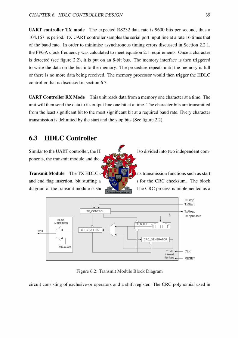
Transmit Module The TX HDLC controller implements transmission functions such as start
and end flag insertion, bit stuffing and FCS generation for the CRC checksum. The block
diagram of the transmit module is shown in figure 6.2. The CRC process is implemented as a
TX_CONTROL
0 7
8
TX_SHIFT
CRC_GENERATOR
BIT_STUFFING
01111110
FLAG INSERTION
TxD
TxInputData TxRead
TxStart TxStop
To all internal flip-flops
CLK
RESET
Figure 6.2: Transmit Module Block Diagram
circuit consisting of exclusive-or operators and a shift register. The CRC polynomial used in

CHAPTER 6. HDLC CONTROLLER DESIGN 40
this project is
CRC-16 = X16 + X15 + X2 + 1. (6.1)
Figure 6.3 illustrates the implementation of CRC-16 polynomial. At any given instance, the
C 15 C 14 . . . C 2 C 1 C 0
Input bits
Figure 6.3: CRC Architecture to Implement Polynomial X16 + X15 + X2 + 1
output of the polynomial is the 16-bit register value calculated from the input bit and the rest
of the register contents. While the transmit module is not reading data from the memory, the
FLAG INSERTION sub-module will continue asserting flags. Once the TxStart is asserted, the
transmit module will start reading the first octet from the memory. The data on the bus is latched
into a shift register TX SHIFT. The data in the shift register will then be shifted out bit-by-bit on
the CLK rising edges. The following procedure occurs:
• While data is being shifted, the CRC GENERATOR calculates the FCS and the BIT STUFFING
sub-module performs bit stuffing process.
• During the shifting of the last octet bit, the TX CONTROL checks for the TxStop signal. If
the TxStop is not asserted, the TxRead is asserted and the TxInputData is latched into
a shift register. The process will repeat until TxStop is asserted.
• Once TxStop is asserted, a multiplexer switches to the CRC GENERATOR input line. The
currently calculated FCS is then shifted out to the TxD line.
Receive Module The receive module implements the required HDLC functions including flag
detection, zero unstuffing and CRC checking. The module is illustrated in figure 6.4. The data
reception process is performed as follows, firstly the character reception synchronisation has to
be established. This is performed by the FLAG DETECT sub-module.
• Once the FLAG DETECT sub-module detect a flag, the receiver bit count is reset. While
flags are being received the receive module stays in an idle mode.
• Once an input data pattern is different from the flag pattern the ZERO UNSTUFF and the
CRC CHK sub-modules are activated.

CHAPTER 6. HDLC CONTROLLER DESIGN 41
7 0 RX_SHIFT
7 0 RX_BUFFER
RX_CONTROL
RxDataWrite
RxOutputData
FLAG_DETECT ZERO
UNSTUFF BIT_CNT
CRC_CHK
RX STATUS
RxD
8
CLK
RESET
To all internal flip-flops
RESEND
Figure 6.4: Receive Module Block Diagram
• While the data reception is occurring, the CRC CHK calculates the FCS using the same
polynomial as the transmitter.
• The ZERO UNSTUFF monitors the input data in the RX BUFFER register. Once a zero that
was inserted by bit stuffing process is detected the shift register and the bit count processes
are halted for one clock cycle. This is how a bit stuffing zero is deleted from the incoming
data.
• After the eighth bit of every non-flag character that is received, the RxDataWrite is
asserted. The one clock cycle RxDataWrite pulse is used by the memory interface pro-
cessor to write the data on the bus into the memory.
• The procedure above continues until a flag is detected. Once detected the calculated 16-
bit FCS is compared with the last two octets that were received. If the two are different
the RESEND signal is asserted.
6.4 Memory Interface Controller
The purpose of the memory interface controller is to ensure that there is no memory bus con-
tention among the four components that need memory access (see figure 6.1). It uses the control
signals from the four components to operate on the data to be written or read from the memory.
Figure 6.5 illustrates the sequence of the four modules. Referring to this figure, the memory
interface controller allocates memory access to the four modules as follows:
• Between time instances t0 and ta none of the modules are active. The HDLC controller is
idling, waiting for data reception.
• At time ta, the first character start-bit is detected and the memory interface controller gives
the service to the TX UART controller. The memory access is reserved to this module

CHAPTER 6. HDLC CONTROLLER DESIGN 42
until the end of data reception. After the last bit is received at time tb, the memory
interface controller waits for few bit periods (between tb and tc) to make sure that there
is no more data coming. Between ta and tc no other module will be allowed access to
the memory. This is done to make sure that both the transmitter and the receiver are not
writing data to the memory simultaneously.
• At tc the memory interface controller triggers (by sending a TxStart signal) the TX
HDLC module and start allocating the memory access whenever the module needs to
fetch a character. Once at tc, even if more data can arrive from the PC, the TX UART will
be denied memory access.
• In order to allow full-duplex operation, from tc onwards the memory interface controller
can allow both the TX HDLC and the RX HDLC memory access simultaneously. Be-
tween the two modules, the priority is given to the TX HDLC.
• As the TX HDLC request data from the memory (by sending TxRead signal), the memory
interface controller increment the FIFO address for each read cycle towards the final
address recorded during the TX UART cycle. Once the final address is reached, the
interface sends a pulse signal (TxStop in figure 6.2) to stop the TX HDLC.
• The RX HDLC starts at time td when a first non flag character is received. At this time, the
RX HDLC sends the first RxDataWrite pulse to the memory interface controller. If the
TX HDLC is still active and the memory reading cycle is not complete, the character to
be written into the memory is buffered, otherwise the RxOutputData is written directly
into the memory. Once the reading cycle is complete the buffered character is written to
the memory.
• The procedure above repeats until a flag is detected (at te).
• At t f , the memory interface controller starts reading and transferring data from the FIFO
memory to the RX UART. The process continues until the last character is read from the
memory at tg.

CHAPTER 6. HDLC CONTROLLER DESIGN 43
TX UART TX HDLC
RX HDLC RX UART time
a b c d 0 e f g
Figure 6.5: The HDLC Timing Diagram
6.5 Simulation Results
Figure 6.6 shows the simulated HDLC controller time series. The waveforms in the figure
illustrate some of the signals explained in section 6.3. The bottom signal in the figure illustrates
the HDLC frame that is transmitted by the TX HDLC to the RX HDLC controller. Also shown
in the figure are the TxInputData, TxStart, TxStop and the RxDataWrite signals. The
Figure 6.6: FPGA Simulation
RxOutputData in figure 6.4 is illustrated by the signal tx sram0 d (the sixth signal from the
top) shown in figure 6.6. Lastly, the RS232 signal that is transmitted by the TNC to the PC is
shown by the top signal in figure 6.6.

CHAPTER 6. HDLC CONTROLLER DESIGN 44
6.6 VHDL Compilation Report
The simulation performed in section 6.5 gives only the logical results of the VHDL design.
Figure 6.7 shows a compiler summary report. As shown in the figure, only 561 of the 12060
Figure 6.7: The VHDL Compilation Report Summary
FPGA total logic elements have been used. With the number of unused logic elements, one can
implement parts of a modem. The combination of an HDLC controller and a modem in the
FPGA can reduce the system complexity and power consumption.
6.7 Conclusion
This chapter discussed not only how the HDLC controller was designed, but also showed the
system end-to-end results. In order to test the functionality of the modem, the HDLC data frame
sent by the TX HDLC module through the modem should be the same as the one received by
the RX HDLC module. The results illustrated in figure 6.6 were obtained by connecting the TX
HDLC output signal directly to the RX HDLC input signal. The terminal was used to transmit
a few characters. These characters were measured with a logic analyser. The 16-bit FCS was
also measured, and compared with the calculated FCS of the transmitted characters.

Chapter 7
Results and Conclusion
7.1 Introduction
In this chapter, the results from the project are discussed. The results are divided into two parts,
the functional results of the system and the results in terms of the project goals. Section 7.2
discusses the implementation of the TNC system. Section 7.3 discusses the functional results
while the project summary is given in section 7.5.
7.2 Implemented System
Figure 7.1 shows the components used for the TNC system. The UART controller, HDLC con-
troller and the processor were implemented in the FPGA. The modem was implemented on a
microcontroller. For data storage, an SRAM with 512K × 8 memory was used. The functional-
ity of these three elements was shown by measuring the end-to-end results of the system.
45

CHAPTER 7. RESULTS AND CONCLUSION 46
PROCESSOR
TX
SRAM
TX
UART controller
RX RX
HDLC Controller
Tx
Rx
TxD
RxD
Analog signal
RxData
TxData Control Signals
Data[0..7]
Data[0..7]
Control Signals
Control signals
Data[0..7]
Control Signal Data[0..7]
Control signals
Data[0..7]
Packet radio modem
FPGA Microcontroller
Figure 7.1: TNC Components Block Diagram
7.3 Functional Results of the Whole System
In order to measure the end to end functionality, a system has to be tested and the output com-
pared to the specifications. As a measure of functionality, the system that was built should
be able transmit and receive a HDLC frame at 9600 bits per second. The functionality of the
system was tested by transmitting text files from a terminal with the following settings:
1. baud rate: 9600
2. Data bits: 8
3. Stop bits: 1
4. Parity bits: 0.
From the terminal settings above, it follows that the number of bits per character including a
start bit, is ten. Figure 7.2 illustrates the transmission and reception of two characters “UN”.
The binary ASCII codes for character U is “01010101” while that of N is “01001110”.

CHAPTER 7. RESULTS AND CONCLUSION 47
Figure 7.2: Transmission and Reception of Two Characters “UN”
Figure 7.2 shows five signals; from bottom to the top, the signals are:
Channel D0 is a waveform of the output of the TX HDLC module to the TX modem. See the
TxD signal in figure 2.1 in chapter 2. The signal shows the transmission of characters
U, N and a 16 bit FCS. The characters are transmitted serially, starting with the least
significant bit. The waveform also illustrates HDLC flag pattern “01111110” delimiting
the frame at both ends.
Channel D2 signal is extracted from channel D0 to illustrate the transmitted data without the
flag fields.
Channel 2 is an analog output of the TX modem to the RX modem. The signal shown is
scrambled by the TX modem.
Channel D1 shows the unscrambled NRZ-L data transmitted from the RX modem to the RX
HDLC controller. See the RxD signal in figure 2.1.
Channel D3 is an RS232 signal transmitted to the PC. Additional to the data being transmitted
are the start and stop bits. The signal represents the RxData signal shown in figure 2.1.
The bitstream patterns of channels D2 and D3 are illustrated in figure 7.3. The start bit (zeros)
and stop bit (ones) are indicated in Channel D3 by bold letters. With the help of start and stop
bits in figure 7.3, the four transmitted characters can be identified as follows:
• The ASCII binary value “01010101” corresponds to a character “U”. This is the first
transmitted character.

CHAPTER 7. RESULTS AND CONCLUSION 48
Channel D 2 :
1 0 1 0 1 0 1 0 0 1 1 1 0 0 1 0 1 0 1 1 1 1 0 0 1 0 1 0 1 0 1 1
Channel D 3 :
0 1 0 1 0 1 0 1 0 1 0 0 1 1 1 0 0 1 0 1 0 1 0 1 1 1 1 0 0 1 0 1 0 1 0 1 0 1 1 1
Figure 7.3: Transmitted Bitstreams
• The second character is “N” with ASCII binary value “01001110”.
• The third character “=” which is the first FCS byte has a binary value “00111101”.
• The last character has an ASCII binary value of “11010101”.
The first two characters represent the data field of the HDLC frame while the last two represent
the FCS field. The creation of the FCS field characters is shown in section 7.3.1.
7.3.1 Frame Check Sequence Field
In this section, the functionality and the results of the FCS generator will be discussed. The
results are discussed in relation with the transmitted data in section 7.3 (see figure 7.3 Channel
D2). Figure 7.4 shows the FCS shift register calculations during the transmission of the charac-
Figure 7.4: FCS Shift Register During Characters “UN” Transmission
ters “UN”. The figure is a table that shows the step-by-step operation of the CRC-16 polynomial
that was discussed in section 6.3. The process begins with the shift register set to all ones, see
columns (C15) through (C0) in row Initial. Each row of the table shows the values of the shift

CHAPTER 7. RESULTS AND CONCLUSION 49
register after one bit period. After the last bit of the data that is being transmitted is shifted in,
the contents of the shift register starting with (C0), is then transmitted as an FCS (shown by last
row in the table).
7.3.2 Bit Stuffing
This section illustrates that the system also performs the bit stuffing that is explained in sec-
tion 2.2.4. To test bit stuffing two characters that have ASCII binary codes of more than five
consecutive ones were transmitted. The two transmitted characters “˜ ” have binary values
“01111101” and “01111110” respectively. Figure 7.5 shows the original bit transmission pat-
tern and the expected bit pattern after bit stuffing is applied. The patterns represent the trans-
mission of the characters “˜ ”. The transmission begins with the least significant bit of the first
character. It ends with the most significant bit of the last character. Figure 7.6 shows measured
Original pattern: 1 0 1 1 1 1 1 0 0 1 1 1 1 1 1 0
After bit stuffing: 1 0 1 1 1 1 1 0 0 0 1 1 1 1 1 0 1 0
Figure 7.5: Bit Stuffing
signals for the transmission of characters “˜ ”. The five channels in figure 7.6 are defined as
those in figure 7.2. The similarity between channel D2 in figure 7.6 and the after bit stuffing pat-
tern in figure 7.5 gives the evidence that transmitter performs bit stuffing as expected. However
the comparison is made only on the data field bits. The FCS field was discussed in section 7.3.1.
The HDLC controller bit unstuffing can evaluated by comparing channel D3 in figure 7.6 with
the original pattern in figure 7.5. With the exception of the added start and stop bits in channel
D3, the signal represents the original pattern in figure 7.5. Sections 7.3 through 7.3.2 gave re-
sults on the functionality of the system. Section 7.5 compares the modem used in this project
with other modems.

CHAPTER 7. RESULTS AND CONCLUSION 50
Figure 7.6: Measured Bit Stuffing Effect
7.4 Performance
This section discusses the maximum clock speed for this solution with the FPGA and SRAM.
The performance measurement of the modem was discussed in section 4.3.
7.4.1 FPGA Performance
The performance of the FPGA was measured by analysing the project’s compilation report. The
timing analyser of the report gives the maximum clock frequency table. Figure 7.7 shows an
extract from the compiler timing analyser report.

CHAPTER 7. RESULTS AND CONCLUSION 51
Figure 7.7: FPGA performance
According to this figure, the maximum frequency for the project is 148.96 MHz.
7.4.2 SRAM Performance
The SRAM performance was evaluated by its writing and reading cycle times. According to
the datasheet of this SRAM, the maximum read and write cycle times are 10 ns [19]. Therefore
the maximum frequency for reading or writing to the SRAM is 100 MHz. The SRAM speed
constraints the maximum rate for the implementation.
7.5 Modem Comparisons
In chapter 2, characteristics of few known packet radio modems were presented. Though the
old modems functioned satisfactorily, new modem designs are still emerging. The reason for
developing newer packet radio modems is not only to improve the performance, but also to
reduce the complexity, power and improve the flexibility of the TNCs. The other reason was
to counteract the older modems component obsolescence problem. In this section, the modem
used for this project is evaluated against the few modems that were discussed in chapter 2.
Complexity The complexity of the circuit can be measured in various ways. In many cases,
the number of components used in a design can be used as a measure for the system complexity.
Assuming that the same components packages and the equal board layers are used, the number
of components is proportional to the board area. Figure 7.8 shows the board areas of the five
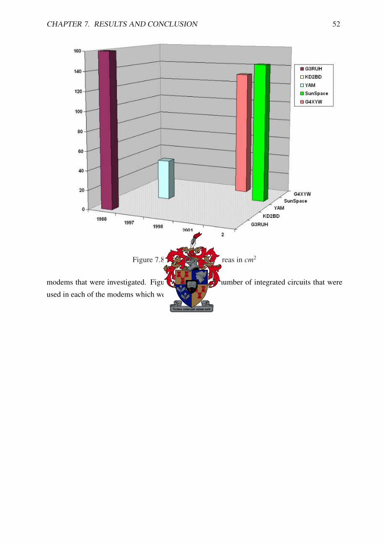
CHAPTER 7. RESULTS AND CONCLUSION 52
Figure 7.8: Modem Board Areas in cm2
modems that were investigated. Figure 7.9 shows the number of integrated circuits that were
used in each of the modems which were investigated.

CHAPTER 7. RESULTS AND CONCLUSION 53
Figure 7.9: Number of Components Per Modem
Power Consumption One of the most important engineering factors in any system design is
power. In many cases, systems are designed with a limited power budget. Also for the sys-
tems that are powered by batteries, the higher the power consumption means the more battery
replacements in a given time. Hence the lower the power of the system, the better the design.
Some of the power values shown in figure 7.10 were given by their modem developers while
others were measured. The conclusion on power consumption can not be drawn from the infor-
mation available. This is because some of the modems power consumption were not given. The
power consumption for the YAM modem which is powered by a connected PC was not given.
The power consumption of the KD2BD was also not given.
Flexibility Flexibility of the system can be measured by the ability to change the operating
characteristics without extensively changing their hardware. For this project the area of interest
was an increase in the baud rate. The following is the analysis of each of the five modems
flexibility:
• The G3RUH processing is only on hardware. The modem is capable of speeds up to
64000 baud [8]. The maximum data rate limit is set by the DAC maximum conversion

CHAPTER 7. RESULTS AND CONCLUSION 54
Figure 7.10: Power Consumption For Each Modem (Watts)
rate. Higher speeds can be implemented by increasing the input clock signal rate and also
changing the anti-alias filter capacitor and resistor values. The numbers of the capacitors
and the resistors that needs to be changed are nine and seven respectively. Every baud
rate needs its specific filter capacitors and resistors.
• The G4XYW modem is based on a microcontroller. However some of the modem func-
tionality such as the anti-alias filter are implemented by hardware. The modem data
rate can be increased by increasing (by software) the microcontroller timer interrupt rate
which acts as a modem clock. The limit of the baud rate is set by the processor execution
time required per bit period. These execution times were discussed in section 4.3. As per
table 4.2, the maximum baud rate of the modem is approximately 38400 bits per second.
The bit rate was calculated by finding a reciprocal of the worst execution time (24 µs)
of the modem. The anti-alias filters of the G4XYW modem are similar to those of the
G3RUH. Hence the filter capacitor and resistors are to be considered when increasing the
baud rate.
• From the modems that were discussed, the YAM modem is special in various ways. First,

CHAPTER 7. RESULTS AND CONCLUSION 55
it is implemented together with the HDLC controller in a FPGA. It does not require the
external power supply; it is powered by the PC which is the transmitter and the receiver
of the data to the HDLC controller. The modem is a G3RUH 9600 baud compatible,
and capable of AFSK 1200 and Manchester-FSK 2400 bauds [9]. The maximum baud
rate of the modem is not given. However the modem flip-flop clock is derived from a
2.4576 MHz crystal oscillator and with the FPGA parallel processing capability, the baud
rate can be higher than that of the G3RUH.
• Both the Sunspace ground station modem and the KD2BD modem are hardware based
and very similar to the G3RUH.
7.6 Conclusion
There are many ways to implement a TNC. Traditional modems that are still functioning satis-
factorily are based entirely on hardware while the recent modems are based on microcontrollers
and FPGAs. The main problem with the traditional modems is the obsolescence of components
and the complexity of their designs. They also consume more power than the microcontroller
and FPGA based modems. This was proved by comparing the consumption of both the G3RUH
and Sunspace modems with that of the G4XYW modem.
The function and performance of the TNC in this project has been verified. The UART,
HDLC controller, and the memory interface controller performed as expected. The G4XYW
modem also performed well and can be upgraded to operate at a speed of 38400 bps.
Power Consumption of the Modem In section 1.1 one of the parameters to improve is the
power consumption. As shown in figure 7.10, compared to the G3RUH and the SunSpace
modems, the power consumption of the G4XYW modem is by far the lowest.
Complexity of the Modem The complexity of the circuit is defined the number of compo-
nents that is used. Referring to figure 7.9 we see that YAM modem which is implemented on a
FPGA is the least complex implementation. After the YAM modem, the second least complex
modem is the G4XYW. The YAM is implemented in hardware descriptive language (HDL)
while the G4XYW modem is implemented in low-level programming language, Assembly. As
compared to the HDLs, the Assembly language programs are difficult to follow. However, the
AVR microcontrollers can be programmed in high-level languages such as C which are simpler
than Assembly. In terms of circuit debugging the circuit with less number of components can

CHAPTER 7. RESULTS AND CONCLUSION 56
be easy to debug. With the exception of Sunspace modem, the number of components per board
is proportional to the board area. The Sunspace modem board area is smaller than that of the
G3RUH modem. This is because the Sunspace used the smaller surface mount components
while the G3RUH used through-hole package components (see figure 2.5).
Flexibility The characteristics of the modem anti-alias filter depends on the baud rate to be
used. All the modems discussed in this project use similar hardware based filters. These filter
circuits are implemented on operational amplifiers connected to resistors and capacitors of spe-
cific magnitudes. Hence there is a need to replace a number of components from the modem
before the current baud rate can be changed. However for the microcontroller and FPGA based
modems, the problem can be solved by implementing software based filters. The possibility of
the software filters can be realised through the high capabilities of the DSP which is also used
in software defined radio (SDR).
7.7 Recommendations
In the recent years, most designers combines HDLC controller and packet radio modem func-
tionalities on one PCB and call the combination as a modem [11, 9]. Most of these modems
are implemented on FPGAs [10, 11, 13]. Based on individuals specifications, the following are
packet radio implementation recommendations:
• The microcontroller based G4XYW modem which was recommended by my study leader
in 2003 was evaluated and can be used for baud rates of up to 38400 bits per second.
• For higher baud rates, where an external modem is required, the FPGA modems can be
used. The parallel processing capabilities of the FPGA can result in high data rates (up to
1 Mbits/s [13]).
• A different approach for packet modem implementation is the one that utilises the flex-
ibility of software and the PC hardware. With this approach a PC sound-card is used
together with a software for packet radio implementation. This implementation is ideal
for applications that do not require external modem.
However for FPGA and microcontroller modems, some work need to be done to solve their
speed dependent analog circuitry problem. Because of the speed dependent analog circuitry,
the performance of the slower AFSK demodulators implemented on the modems designed for
FSK is unsatisfactory [11].

Appendix A
HDLC VHDL Code
% Author: Sello Seabe
% Student number: 14011018-2002
% Function: All the modules that implements HDLC controller
LIBRARY IEEE;
USE IEEE.STD_LOGIC_1164.ALL;
USE IEEE.STD_LOGIC_UNSIGNED.ALL;
ENTITY project IS
PORT(
clk : IN STD_LOGIC;
reset : IN STD_LOGIC;
RxClock : IN STD_LOGIC;
TX_RS232 : IN STD_LOGIC;
Rx : OUT STD_LOGIC;
rxd : IN STD_LOGIC;
TxD : OUT STD_LOGIC;
Tx : OUT STD_LOGIC;
RX_RS232 : OUT STD_LOGIC;
SRAM0_D : INOUT STD_LOGIC_VECTOR(7 DOWNTO 0);
SRAM0_A : OUT STD_LOGIC_VECTOR(17 DOWNTO 0);
SRAM0_OE : OUT STD_LOGIC;
SRAM0_WE : OUT STD_LOGIC;
SRAM0_UB : OUT STD_LOGIC;
SRAM0_LB : OUT STD_LOGIC;
57

APPENDIX A. HDLC VHDL CODE 58
SRAM0_E : OUT STD_LOGIC
);
END project;
ARCHITECTURE a OF project IS
SIGNAL t_level_reset : STD_LOGIC;
SIGNAL t_level_ireset : STD_LOGIC;
SIGNAL t_level_TX_RS232 : STD_LOGIC;
SIGNAL t_level_RX_RS232 : STD_LOGIC;
SIGNAL t_level_clk : STD_LOGIC;
SIGNAL t_level_uart_rx_data : STD_LOGIC_VECTOR(7 DOWNTO 0);
SIGNAL t_level_tx_data_valid : STD_LOGIC;
---
SIGNAL t_level_uart_tx_data : STD_LOGIC_VECTOR(7 DOWNTO 0);
SIGNAL t_level_TxInputData : STD_LOGIC_VECTOR(7 DOWNTO 0);
SIGNAL t_level_fcst: STD_LOGIC_VECTOR(15 DOWNTO 0);
SIGNAL t_level_crc_input : STD_LOGIC;
SIGNAL t_level_fcs_reset : STD_LOGIC;
SIGNAL t_level_tx_start : STD_LOGIC;
SIGNAL t_level_tx_stop : STD_LOGIC;
SIGNAL t_level_tx_read : STD_LOGIC;
SIGNAL t_level_rx_busy : STD_LOGIC;
SIGNAL t_level_tx_busy : STD_LOGIC;
SIGNAL t_level_proc_enable: STD_LOGIC;
SIGNAL t_level_rxd : STD_LOGIC;
SIGNAL t_level_RxOutputData : STD_LOGIC_VECTOR(7 DOWNTO 0);
SIGNAL t_level_RxDataWrite : STD_LOGIC;
SIGNAL t_level_tx_SRAM0_D : STD_LOGIC_VECTOR(7 DOWNTO 0);
SIGNAL t_level_tx_SRAM0_A : STD_LOGIC_VECTOR(17 DOWNTO 0);
SIGNAL t_level_tx_SRAM0_WE : STD_LOGIC;
SIGNAL t_level_tx_SRAM0_OE : STD_LOGIC;

APPENDIX A. HDLC VHDL CODE 59
SIGNAL t_level_tx_SRAM0_E : STD_LOGIC;
SIGNAL t_level_start_uart_rx : STD_LOGIC;
SIGNAL t_level_RxDataRead : STD_LOGIC;
SIGNAL t_level_stop_uart_rx : STD_LOGIC;
SIGNAL t_level_Uart_clk : STD_LOGIC;
SIGNAL t_level_rxclk : STD_LOGIC;
SIGNAL t_level_RxClock :STD_LOGIC;
SIGNAL t_level_RxClock_in :STD_LOGIC;
SIGNAL t_level_rx_sclk : STD_LOGIC;
SIGNAL t_level_tx_clk : STD_LOGIC;
SIGNAL t_level_crc_reset : STD_LOGIC;
SIGNAL t_level_crc_byte : STD_LOGIC;
SIGNAL t_level_resend : STD_LOGIC;
SIGNAL t_level_r_buffer : STD_LOGIC_VECTOR(7 DOWNTO 0);
SIGNAL t_level_fcs : STD_LOGIC_VECTOR(15 DOWNTO 0);
SIGNAL t_level_SRAM0_OE : STD_LOGIC;
SIGNAL t_level_SRAM0_WE : STD_LOGIC;
SIGNAL t_level_SRAM0_UB : STD_LOGIC;
SIGNAL t_level_SRAM0_LB : STD_LOGIC;
SIGNAL t_level_SRAM0_E : STD_LOGIC;
SIGNAL t_level_SRAM0_A : STD_LOGIC_VECTOR(17 DOWNTO 0);
SIGNAL t_level_SRAM0_D : STD_LOGIC_VECTOR(7 DOWNTO 0);
SIGNAL t_level_SRAM0_D1 : STD_LOGIC_VECTOR(7 DOWNTO 0);
COMPONENT tx_uart
PORT (
clk : IN STD_LOGIC;
ireset : IN STD_LOGIC;
TX_RS232 : IN STD_LOGIC;
uart_tx_data : OUT STD_LOGIC_VECTOR(7 DOWNTO 0);
tx_data_valid : OUT STD_LOGIC;
proc_enable : OUT STD_LOGIC;
oUart_clk : OUT STD_LOGIC

APPENDIX A. HDLC VHDL CODE 60
);
END COMPONENT;
COMPONENT rx_uart
PORT(
ireset : IN STD_LOGIC;
tx_sclk : IN STD_LOGIC;
tx_clk : IN STD_LOGIC;
start_uart_rx : IN STD_LOGIC;
stop_uart_rx : IN STD_LOGIC;
uart_rx_data : IN STD_LOGIC_VECTOR(7 DOWNTO 0);
RxDataRead : OUT STD_LOGIC;
Rx : OUT STD_LOGIC;
RX_RS232 : OUT STD_LOGIC
);
END COMPONENT;
COMPONENT hdlc_rx
PORT
(
rx_sclk : IN STD_LOGIC;
ireset : IN STD_LOGIC;
RxClock : IN STD_LOGIC;
rxd : IN STD_LOGIC;
fcs : IN STD_loGIC_VECTOR(15 DOWNTO 0);
RxOutputData : OUT STD_LOGIC_VECTOR(7 DOWNTO 0);
tx_clk : OUT STD_LOGIC;
crc_reset : OUT STD_LOGIC;
crc_byte : OUT STD_LOGIC;
resend : OUT STD_LOGIC;
r_buffer_out : OUT STD_LOGIC_VECTOR(7 DOWNTO 0);
RxDataWrite : OUT STD_LOGIC
);
END COMPONENT;
APPENDIX A. HDLC VHDL CODE 61
COMPONENT crc_rx
PORT(
x8_sclk : IN STD_LOGIC;
rxclk : IN STD_LOGIC;
ireset : IN STD_LOGIC;
crc_reset : IN STD_LOGIC;
crc_byte : IN STD_LOGIC;
r_buffer : IN STD_LOGIC_VECTOR(7 DOWNTO 0);
fcs_2 : OUT STD_LOGIC_VECTOR(15 DOWNTO 0)
);
END COMPONENT;
COMPONENT crc
PORT(
uart_clk : IN STD_LOGIC;
bit_clk : IN STD_LOGIC;
crc_input : IN STD_LOGIC;
fcs_reset : IN STD_LOGIC;
fcs : OUT STD_LOGIC_VECTOR(15 DOWNTO 0)
);
END COMPONENT;
COMPONENT clk_src
PORT(
clk : IN STD_LOGIC;
reset : IN STD_LOGIC;
RxClock : IN STD_LOGIC;
ireset : OUT STD_LOGIC;
rx_sclk : OUT STD_LOGIC
);
END COMPONENT;
COMPONENT proc
PORT(
uart_clk : IN STD_LOGIC;

APPENDIX A. HDLC VHDL CODE 62
ireset : IN STD_LOGIC;
proc_enable : IN STD_LOGIC;
tx_data_valid : IN STD_LOGIC;
tx_busy : IN STD_LOGIC;
uart_rx_data : IN STD_LOGIC_VECTOR(7 DOWNTO 0);
TxInputData : OUT STD_LOGIC_VECTOR(7 DOWNTO 0);
tx_start : OUT STD_LOGIC;
tx_stop : OUT STD_LOGIC;
hdlc_read : IN STD_LOGIC;
rx_busy : OUT STD_LOGIC;
uart_tx_data : OUT STD_LOGIC_VECTOR(7 DOWNTO 0);
start_uart_rx : IN STD_LOGIC;
RxDataRead : IN STD_LOGIC;
tx_SRAM0_D : IN STD_LOGIC_VECTOR(7 DOWNTO 0);--INOUT
tx_SRAM0_WE : IN STD_LOGIC;
tx_SRAM0_OE : IN STD_LOGIC;
tx_SRAM0_E : IN STD_LOGIC;
tx_SRAM0_A : IN STD_LOGIC_VECTOR(17 DOWNTO 0);
SRAM0_D1 : IN STD_LOGIC_VECTOR(7 DOWNTO 0);
SRAM0_D : INOUT STD_LOGIC_VECTOR(7 DOWNTO 0);
SRAM0_OE : OUT STD_LOGIC;
SRAM0_WE : OUT STD_LOGIC;
SRAM0_UB : OUT STD_LOGIC;
SRAM0_LB : OUT STD_LOGIC;
SRAM0_E : OUT STD_LOGIC;
SRAM0_A : OUT STD_LOGIC_VECTOR(17 DOWNTO 0)
);
END COMPONENT;
COMPONENT proc_rx
PORT(
tx_sclk : IN STD_LOGIC;
tx_clk : IN STD_LOGIC;
ireset : IN STD_LOGIC;

APPENDIX A. HDLC VHDL CODE 63
RxDataWrite : IN STD_LOGIC;
RxDataRead : IN STD_LOGIC;
rx_busy : IN STD_LOGIC;
RxOutputData : IN STD_LOGIC_VECTOR(7 DOWNTO 0);
tx_busy : OUT STD_LOGIC;
start_uart_rx : OUT STD_LOGIC;
stop_uart_tx : OUT STD_LOGIC;
tx_SRAM0_D : OUT STD_LOGIC_VECTOR(7 DOWNTO 0);--INOUT
tx_SRAM0_OE : OUT STD_LOGIC;
tx_SRAM0_WE : OUT STD_LOGIC;
tx_SRAM0_E : OUT STD_LOGIC;
tx_SRAM0_A : OUT STD_LOGIC_VECTOR(17 DOWNTO 0)
);
END COMPONENT;
COMPONENT hdlc_tx
PORT(
ireset : IN STD_LOGIC;
clk : IN STD_LOGIC;
uart_clk : IN STD_LOGIC;
bit_clk : IN STD_LOGIC;
tx_start : IN STD_LOGIC;
tx_stop : IN STD_LOGIC;
TxInputData : IN STD_LOGIC_VECTOR(7 DOWNTO 0);
fcs : IN STD_LOGIC_VECTOR(15 DOWNTO 0);
RxClock_in : OUT STD_LOGIC;
crc_input : OUT STD_LOGIC;
fcs_reset : OUT STD_LOGIC;
tx_read : OUT STD_LOGIC;
Tx : OUT STD_LOGIC;
HDLC_TX : OUT STD_LOGIC
);
END COMPONENT;
BEGIN

APPENDIX A. HDLC VHDL CODE 64
U8 : proc
PORT MAP(
uart_clk => t_level_Uart_clk,
ireset => t_level_ireset,
proc_enable => t_level_proc_enable,
tx_data_valid => t_level_tx_data_valid,
uart_rx_data => t_level_uart_tx_data,
tx_start => t_level_tx_start,
tx_stop => t_level_tx_stop,
rx_busy => t_level_rx_busy,
tx_busy => t_level_tx_busy,
TxInputData => t_level_TxInputData,
hdlc_read => t_level_tx_read,
uart_tx_data => t_level_uart_tx_data,
start_uart_rx => t_level_start_uart_rx,
RxDataRead => t_level_RxDataRead,
tx_SRAM0_D => t_level_tx_SRAM0_D,
tx_SRAM0_WE => t_level_tx_SRAM0_WE,
tx_SRAM0_OE => t_level_tx_SRAM0_OE,
tx_SRAM0_E => t_level_tx_SRAM0_E,
tx_SRAM0_A => t_level_tx_SRAM0_A,
SRAM0_OE => t_level_SRAM0_OE,
SRAM0_WE => t_level_SRAM0_WE,
SRAM0_UB => t_level_SRAM0_UB,
SRAM0_LB => t_level_SRAM0_LB,
SRAM0_E => t_level_SRAM0_E,
SRAM0_A => t_level_SRAM0_A,
SRAM0_D1 => t_level_SRAM0_D1,
SRAM0_D => t_level_SRAM0_D
);
U11 : proc_rx
PORT MAP(

APPENDIX A. HDLC VHDL CODE 65
tx_sclk => t_level_rx_sclk,
tx_clk => t_level_tx_clk,
ireset => t_level_ireset,
RxDataWrite => t_level_RxDataWrite,
RxDataRead => t_level_RxDataRead,
rx_busy => t_level_rx_busy,
tx_busy => t_level_tx_busy,
RxOutputData => t_level_RxOutputData,
start_uart_rx => t_level_start_uart_rx,
stop_uart_tx => t_level_stop_uart_rx,
tx_SRAM0_D => t_level_tx_SRAM0_D,
tx_SRAM0_WE => t_level_tx_SRAM0_WE,
tx_SRAM0_OE => t_level_tx_SRAM0_OE,
tx_SRAM0_E => t_level_tx_SRAM0_E,
tx_SRAM0_A => t_level_tx_SRAM0_A
);
U4 : hdlc_tx
PORT MAP(
ireset => t_level_ireset,
clk => t_level_clk,
uart_clk => t_level_Uart_clk,
bit_clk => t_level_proc_enable,
tx_start => t_level_tx_start,
tx_stop => t_level_tx_stop,
TxInputData => t_level_TxInputData,
fcs => t_level_fcst,
crc_input => t_level_crc_input,
RxClock_in => t_level_RxClock_in,
fcs_reset => t_level_fcs_reset,
tx_read => t_level_tx_read,
HDLC_TX => TxD,
Tx => Tx
);

APPENDIX A. HDLC VHDL CODE 66
U1 : clk_src
clk => t_level_clk,
RxClock => t_level_RxClock,
reset => t_level_reset,
ireset => t_level_ireset,
rx_sclk => t_level_rx_sclk
);
U2 : tx_uart
PORT MAP (
ireset => t_level_ireset,
TX_RS232 => t_level_TX_RS232,
clk => t_level_clk,
oUart_clk => t_level_Uart_clk,
proc_enable => t_level_proc_enable,
uart_tx_data => t_level_uart_tx_data,
tx_data_valid => t_level_tx_data_valid
);
U3: rx_uart
PORT MAP(
ireset => t_level_ireset,
tx_sclk => t_level_rx_sclk,
tx_clk => t_level_tx_clk,
start_uart_rx => t_level_start_uart_rx,
RxDataRead => t_level_RxDataRead,
stop_uart_rx => t_level_stop_uart_rx,
uart_rx_data => t_level_uart_rx_data,
Rx => Rx,
RX_RS232 => t_level_RX_RS232
);
U6 : hdlc_rx
PORT MAP(
rx_sclk => t_level_rx_sclk,

APPENDIX A. HDLC VHDL CODE 67
ireset => t_level_ireset,
RxClock => t_level_RxClock,
rxd => t_level_rxd,
RxOutputData => t_level_RxOutputData,
tx_clk => t_level_tx_clk,
RxDataWrite => t_level_RxDataWrite,
fcs => t_level_fcs,
resend => t_level_resend,
crc_reset => t_level_crc_reset,
crc_byte => t_level_crc_byte,
r_buffer_out => t_level_r_buffer
);
U7: crc_rx
PORT MAP (
x8_sclk => t_level_rx_sclk,
rxclk => t_level_tx_clk,
ireset => t_level_ireset,
crc_reset => t_level_crc_reset,
fcs_2 => t_level_fcs,
crc_byte => t_level_crc_byte,
r_buffer => t_level_r_buffer
);
U5: crc
PORT MAP (
uart_clk => t_level_Uart_clk,
bit_clk => t_level_proc_enable,
crc_input => t_level_crc_input,
fcs_reset => t_level_fcs_reset,
fcs => t_level_fcst
);
t_level_reset <= reset;
t_level_clk <= clk;

APPENDIX A. HDLC VHDL CODE 68
t_level_TX_RS232 <= TX_RS232;
SRAM0_OE <= t_level_SRAM0_OE;
SRAM0_WE <= t_level_SRAM0_WE;
SRAM0_UB <= t_level_SRAM0_UB;
SRAM0_LB <= t_level_SRAM0_LB;
SRAM0_E <= t_level_SRAM0_E;
SRAM0_A <= t_level_SRAM0_A;
SRAM0_D <= t_level_SRAM0_D;
RX_RS232 <= t_level_RX_RS232;
t_level_SRAM0_D1 <= SRAM0_D;
t_level_RxClock <= t_level_RxClock_in;
END a;
LIBRARY IEEE;
USE IEEE.STD_LOGIC_1164.ALL;
USE IEEE.STD_LOGIC_UNSIGNED.ALL;
--USE IEEE. STD_LOGIC_ARITH.ALL;
--USE IEEE.NUMERIC_STD.ALL;
ENTITY clk_src IS
PORT
(
clk : IN STD_LOGIC;
reset : IN STD_LOGIC;
RxClock : IN STD_LOGIC;
ireset : OUT STD_LOGIC;
rx_sclk : OUT STD_LOGIC
);
END clk_src;
ARCHITECTURE a OF clk_src IS
SIGNAL iireset : STD_LOGIC;
SIGNAL x8_cnt : STD_LOGIC_VECTOR(7 DOWNTO 0);

APPENDIX A. HDLC VHDL CODE 69
SIGNAL x8_sclk : STD_LOGIC;
SIGNAL iiRxClock : STD_LOGIC;
SIGNAL iRxClock : STD_LOGIC;
BEGIN
sync_reset:
PROCESS (reset,clk)
VARIABLE ireset_reg : STD_LOGIC_VECTOR(2 DOWNTO 0);
BEGIN
IF reset = ’0’ THEN
ireset_reg := (OTHERS => ’0’);
iireset <= ’0’;
ELSIF clk’event AND clk = ’1’ THEN
iireset <= ireset_reg(0);
ireset_reg := ’1’ & ireset_reg(2) & ireset_reg(1);
END IF;
END PROCESS sync_reset;
PROCESS(clk, RxClock, iireset)
BEGIN
IF iireset = ’0’ THEN
iRxClock <= ’1’;
iiRxClock <= ’1’;
ELSIF clk’event AND clk = ’1’ THEN
iiRxClock <= RxClock;
iRxClock <= iiRxClock;
END IF;
END PROCESS;
PROCESS(clk,iireset,RxClock)
BEGIN
IF iireset = ’0’ THEN
x8_cnt <= (OTHERS => ’0’);
x8_sclk <= ’1’;

APPENDIX A. HDLC VHDL CODE 70
ELSIF clk’event AND clk = ’1’ THEN
IF x8_cnt = 16#A1# THEN -- 20ns x 162 = 3.24us [1/(2x16x9600)]
x8_sclk <= NOT(x8_sclk);
x8_cnt <= (OTHERS => ’0’); --------
ELSIF RxClock = ’1’ AND iRxClock = ’0’ THEN -- 0 to 1 transition detected
x8_sclk <= ’1’;
x8_cnt <= "00000010";
ELSE
x8_cnt <= x8_cnt + 1;
END IF;
END IF;
END PROCESS;
ireset <= iireset;
rx_sclk <= x8_sclk;
END a;
--
LIBRARY IEEE;
USE IEEE.STD_LOGIC_1164.ALL;
USE IEEE.STD_LOGIC_UNSIGNED.ALL;
ENTITY tx_uart IS
PORT
(
clk : IN STD_LOGIC;
ireset : IN STD_LOGIC;
TX_RS232 : IN STD_LOGIC;
uart_tx_data : OUT STD_LOGIC_VECTOR(7 DOWNTO 0);
tx_data_valid : OUT STD_LOGIC;
proc_enable : OUT STD_LOGIC;
oUart_clk : OUT STD_LOGIC
);

APPENDIX A. HDLC VHDL CODE 71
END tx_uart;
ARCHITECTURE a OF tx_uart IS
TYPE uart_tx_state is (next_start_bit,tx_start_bit,char_bit_samples,stop_bit_samples);
SIGNAL uart_state: uart_tx_state;
SIGNAL uart_clk_cnt : STD_LOGIC_VECTOR(7 DOWNTO 0);
SIGNAL tx_shift_reg : STD_LOGIC_VECTOR(9 DOWNTO 0);
SIGNAL bit_samples_cnt : STD_LOGIC_VECTOR(3 DOWNTO 0);
SIGNAL bit_samples : STD_LOGIC_VECTOR(1 DOWNTO 0);
SIGNAL tx_bit_cnt : STD_LOGIC_VECTOR(3 DOWNTO 0);
SIGNAL uart_clk : STD_LOGIC;
SIGNAL sync_cnt : STD_LOGIC_VECTOR(1 DOWNTO 0);
SIGNAL baud_cnt : STD_LOGIC_VECTOR(11 DOWNTO 0);
SIGNAL pclk : STD_LOGIC;
SIGNAL TX_RS232_t : STD_LOGIC;
SIGNAL TX_RS232_holder : STD_LOGIC;
SIGNAL start_bit_detect : STD_LOGIC;
BEGIN
catch_TX_RS232:
PROCESS(ireset,clk)
BEGIN
IF ireset = ’0’ THEN
TX_RS232_t <= ’1’;
TX_RS232_holder <= ’1’;
ELSIF clk’event AND clk = ’1’ THEN
TX_RS232_holder <= TX_RS232;
TX_RS232_t <= TX_RS232_holder;
END IF;
END PROCESS catch_TX_RS232;
clocks_pr:
PROCESS(ireset,clk)

APPENDIX A. HDLC VHDL CODE 72
BEGIN
IF ireset = ’0’ THEN
uart_clk_cnt <= (OTHERS => ’0’);
uart_clk <= ’1’;
ELSIF clk’event AND clk = ’1’ THEN
----------- Clock generation --------------------------
IF uart_clk_cnt = 16#A1# THEN
-- 20ns x 162 = 3.24us [1/(2x16x9600)]
uart_clk <= NOT(uart_clk);
uart_clk_cnt <= (OTHERS => ’0’);
ELSIF TX_RS232 = ’0’ AND sync_cnt = 2 THEN
uart_clk_cnt <= "00000011";
ELSE
uart_clk_cnt <= uart_clk_cnt + 1;
END IF;
END IF;
END PROCESS clocks_pr;
uart_resync_pr:
PROCESS(clk,ireset)
BEGIN
IF ireset = ’0’ THEN
sync_cnt <= (OTHERS => ’0’);
ELSIF clk’event AND clk = ’1’ THEN
----------- Synchronisation ---------------------
IF TX_RS232_t = ’1’ AND TX_RS232 = ’0’ THEN
sync_cnt <= sync_cnt + 1; -----
ELSIF TX_RS232 = ’1’ AND sync_cnt = 1 THEN
sync_cnt <= (OTHERS => ’0’);
ELSIF TX_RS232 = ’0’ AND sync_cnt = 1 THEN
sync_cnt <= sync_cnt + 1;
ELSIF TX_RS232 = ’1’ AND sync_cnt = 2 THEN
sync_cnt <= (OTHERS => ’0’);
ELSIF TX_RS232 = ’0’ AND sync_cnt = 2 THEN
sync_cnt <= (OTHERS => ’0’);

APPENDIX A. HDLC VHDL CODE 73
END IF;
END IF;
END PROCESS uart_resync_pr;
start_bit_detect_pr: -- For testing UART only
PROCESS(uart_clk,ireset)
BEGIN
IF ireset = ’0’ THEN
start_bit_detect <= ’1’;
ELSIF uart_clk’event AND uart_clk = ’1’ THEN
IF uart_state = stop_bit_samples THEN
start_bit_detect <= ’1’;
ELSIF TX_RS232 = ’0’ THEN -- 0 to 1 transition detected
start_bit_detect <= ’0’;
END IF;
END IF;
END PROCESS start_bit_detect_pr;
bit_rate_clk:
PROCESS(clk,ireset)
BEGIN
IF ireset = ’0’ THEN
pclk <= ’1’;
baud_cnt <= (OTHERS => ’0’);
ELSIF clk’event AND clk = ’1’ THEN
IF baud_cnt = 16#A2B# THEN -- 20ns x 2604 = 52.06us [1/(2x9600)]
pclk <= NOT(pclk);
baud_cnt <= (OTHERS => ’0’);
ELSE
baud_cnt <= baud_cnt + 1;
END IF;
END IF;
END PROCESS bit_rate_clk;
PROCESS (clk,uart_clk,ireset)

APPENDIX A. HDLC VHDL CODE 74
BEGIN
IF ireset = ’0’ THEN
tx_shift_reg <= (OTHERS => ’0’);
ELSIF uart_clk’event AND uart_clk = ’1’ THEN
CASE bit_samples_cnt IS
WHEN "1011" => -- 11
IF bit_samples < 2 THEN
tx_shift_reg <= ’0’ & tx_shift_reg(9 downto 1);
ELSE
tx_shift_reg <= ’1’ & tx_shift_reg(9 downto 1);
END IF;
WHEN OTHERS =>
null;
END CASE;
END IF;
END PROCESS;
PROCESS (clk,uart_clk,ireset)
BEGIN
IF ireset = ’0’ THEN
tx_bit_cnt <= (OTHERS => ’0’);
ELSIF uart_clk’event AND uart_clk = ’1’ THEN
CASE bit_samples_cnt IS
WHEN "1011" => -- 11
IF uart_state = tx_start_bit OR uart_state = stop_bit_samples THEN
tx_bit_cnt <= "0000";
ELSE
tx_bit_cnt <= tx_bit_cnt + 1;
END IF;
WHEN OTHERS =>
null;
END CASE;
END IF;
END PROCESS;

APPENDIX A. HDLC VHDL CODE 75
PROCESS (clk,uart_clk,ireset)
BEGIN
IF ireset = ’0’ THEN
uart_tx_data <= (OTHERS => ’0’);
ELSIF uart_clk’event AND uart_clk = ’1’ THEN
IF uart_state = stop_bit_samples AND bit_samples_cnt = 15 THEN
uart_tx_data <= tx_shift_reg(8 downto 1);
ELSE
null;
END IF;
END IF;
END PROCESS;
PROCESS (clk,uart_clk,ireset)
BEGIN
IF ireset = ’0’ THEN
bit_samples <= (OTHERS => ’0’);
ELSIF uart_clk’event AND uart_clk = ’1’ THEN
CASE bit_samples_cnt IS
WHEN "1000"|"1001"|"1010" => --8 to 10 (sampling)
IF TX_RS232 = ’1’ THEN
bit_samples <= bit_samples + 1;
ELSIF TX_RS232 = ’0’ THEN
bit_samples <= bit_samples;
END IF;
WHEN "1111" => -- 15
bit_samples <= (OTHERS => ’0’);
WHEN OTHERS =>
bit_samples <= bit_samples;
END CASE;
END IF;
END PROCESS;
PROCESS (clk,uart_clk,ireset)
BEGIN

APPENDIX A. HDLC VHDL CODE 76
IF ireset = ’0’ THEN
bit_samples_cnt <= (OTHERS => ’0’);
ELSIF uart_clk’event AND uart_clk = ’1’ THEN
CASE uart_state IS
WHEN next_start_bit =>
IF TX_RS232 = ’0’ THEN
bit_samples_cnt <= "0001";
ELSE
bit_samples_cnt <= bit_samples_cnt + 1;
END IF;
WHEN OTHERS =>
bit_samples_cnt <= bit_samples_cnt + 1;
END CASE;
END IF;
END PROCESS;
PROCESS (clk,uart_clk,ireset)
BEGIN
IF ireset = ’0’ THEN
tx_data_valid <= ’1’;
ELSIF uart_clk’event AND uart_clk = ’1’ THEN
IF uart_state /= stop_bit_samples THEN
tx_data_valid <= ’1’;
ELSIF bit_samples_cnt = 15 AND uart_state = stop_bit_samples THEN
IF bit_samples >= 2 THEN
tx_data_valid <= ’0’;
ELSE
tx_data_valid <= ’1’;
END IF;
END IF;
END IF;
END PROCESS;
PROCESS (clk,uart_clk,ireset)
BEGIN
APPENDIX A. HDLC VHDL CODE 77
IF ireset = ’0’ THEN
uart_state <= next_start_bit;
ELSIF uart_clk’event AND uart_clk = ’1’ THEN
CASE uart_state IS
WHEN next_start_bit =>
IF TX_RS232 = ’0’ THEN
uart_state <= tx_start_bit;
ELSE
uart_state <= next_start_bit;
END IF;
WHEN tx_start_bit =>
CASE bit_samples_cnt IS
WHEN "1011" => -- 11
IF bit_samples > 1 THEN
uart_state <= next_start_bit;
ELSIF bit_samples < 2 THEN
uart_state <= tx_start_bit;
END IF;
WHEN "1111" => -- 15
uart_state <= char_bit_samples;
WHEN OTHERS =>
uart_state <= tx_start_bit;
END CASE;
WHEN char_bit_samples =>
CASE bit_samples_cnt IS
WHEN "1111" => -- 15
IF tx_bit_cnt = 8 THEN
uart_state <= stop_bit_samples;
ELSE
uart_state <= char_bit_samples;
END IF;
WHEN OTHERS =>
uart_state <= char_bit_samples;
END CASE;
WHEN stop_bit_samples =>

APPENDIX A. HDLC VHDL CODE 78
CASE bit_samples_cnt IS
WHEN "1111" => -- 15
uart_state <= next_start_bit;
WHEN OTHERS =>
uart_state <= stop_bit_samples;
END CASE;
END CASE;
END IF;
END PROCESS;
PROCESS(clk,uart_clk,ireset)
BEGIN
IF ireset = ’0’ THEN
proc_enable <= ’0’;
ELSIF uart_clk’event AND uart_clk = ’1’ THEN
IF bit_samples_cnt = 15 THEN
proc_enable <= ’1’;
ELSE
proc_enable <= ’0’;
END IF;
END IF;
END PROCESS;
oUart_clk <= uart_clk;
END a;
--
LIBRARY IEEE;
USE IEEE.STD_LOGIC_1164.ALL;
USE IEEE.STD_LOGIC_UNSIGNED.ALL;
ENTITY rx_uart IS
PORT

APPENDIX A. HDLC VHDL CODE 79
(
ireset : IN STD_LOGIC;
tx_sclk : IN STD_LOGIC;
tx_clk : IN STD_LOGIC;
start_uart_rx : IN STD_LOGIC;
stop_uart_rx : IN STD_LOGIC;
uart_rx_data : IN STD_LOGIC_VECTOR(7 DOWNTO 0);
RxDataRead : OUT STD_LOGIC;
Rx : OUT STD_LOGIC;
RX_RS232 : OUT STD_LOGIC
);
END rx_uart;
ARCHITECTURE a OF rx_uart IS
TYPE uart_rx_state is (rx_uart_idle,rx_uart_info,rx_uart_last);
SIGNAL uart_state: uart_rx_state;
SIGNAL rx_shift_reg : STD_LOGIC_VECTOR(9 DOWNTO 0);
SIGNAL rx_shift_cnt : STD_LOGIC_VECTOR(3 DOWNTO 0);
BEGIN
PROCESS(tx_sclk,ireset,tx_clk)
BEGIN
IF ireset = ’0’ THEN
rx_shift_reg <= (OTHERS => ’1’);
ELSIF tx_sclk’event AND tx_sclk = ’1’ AND tx_clk = ’1’ THEN
CASE uart_state IS
WHEN rx_uart_idle =>
IF start_uart_rx = ’0’ THEN
rx_shift_reg <= ’1’ & uart_rx_data & ’0’;
ELSE
rx_shift_reg <= (OTHERS => ’1’);
END IF;
WHEN rx_uart_last =>
rx_shift_reg <= ’1’ & rx_shift_reg(9 DOWNTO 1);
WHEN OTHERS =>

APPENDIX A. HDLC VHDL CODE 80
IF rx_shift_cnt = 9 THEN --AND info_finished = ’1’ THEN
rx_shift_reg <= ’1’ & uart_rx_data & ’0’;
ELSIF rx_shift_cnt < 9 THEN
rx_shift_reg <= ’1’ & rx_shift_reg(9 DOWNTO 1);
END IF;
END CASE;
END IF;
END PROCESS;
PROCESS(tx_sclk,ireset,tx_clk)
BEGIN
IF ireset = ’0’ THEN
rx_shift_cnt <= (OTHERS => ’0’);
ELSIF tx_sclk’event AND tx_sclk = ’1’ AND tx_clk = ’1’ THEN
CASE uart_state IS
WHEN rx_uart_info =>
IF rx_shift_cnt = 9 THEN--AND info_finished = ’1’ THEN
rx_shift_cnt <= (OTHERS => ’0’);
ELSE
rx_shift_cnt <= rx_shift_cnt + 1;
END IF;
WHEN rx_uart_last =>
IF rx_shift_cnt = 9 THEN
rx_shift_cnt <= (OTHERS => ’0’);
ELSE
rx_shift_cnt <= rx_shift_cnt + 1;
END IF;
WHEN OTHERS =>
rx_shift_cnt <= (OTHERS => ’0’);
END CASE;
END IF;
END PROCESS;
UART_DATA_TRANSMISSION:
PROCESS(tx_sclk,ireset,tx_clk)

APPENDIX A. HDLC VHDL CODE 81
BEGIN
IF ireset = ’0’ THEN
uart_state <= rx_uart_idle;
ELSIF tx_sclk’event AND tx_sclk = ’1’ AND tx_clk = ’1’ THEN
CASE uart_state IS
WHEN rx_uart_idle =>
IF start_uart_rx = ’0’ THEN
uart_state <= rx_uart_info;
ELSE
uart_state <= rx_uart_idle;
END IF;
WHEN rx_uart_info =>
IF stop_uart_rx = ’0’ THEN
uart_state <= rx_uart_last;
ELSE
uart_state <= rx_uart_info;
END IF;
WHEN rx_uart_last =>
IF rx_shift_cnt = 9 THEN
uart_state <= rx_uart_idle;
ELSE
uart_state <= rx_uart_last;
END IF;
WHEN OTHERS =>
uart_state <= rx_uart_idle;
END CASE;
END IF;
END PROCESS UART_DATA_TRANSMISSION;
PROCESS(tx_sclk,ireset,tx_clk)
BEGIN
IF ireset = ’0’ THEN
RxDataRead <= ’1’;
ELSIF tx_sclk’event AND tx_sclk = ’1’ AND tx_clk = ’1’ THEN
CASE uart_state IS

APPENDIX A. HDLC VHDL CODE 82
WHEN rx_uart_info =>
IF rx_shift_cnt = 8 THEN
RxDataRead <= ’0’;
ELSE
RxDataRead <= ’1’;
END IF;
WHEN OTHERS =>
RxDataRead <= ’1’;
END CASE;
END IF;
END PROCESS;
RX_RS232 <= rx_shift_reg(0);
Rx <= rx_shift_reg(0);
END a;
--
LIBRARY IEEE;
USE IEEE.STD_LOGIC_1164.ALL;
USE IEEE.STD_LOGIC_UNSIGNED.ALL;
USE IEEE.STD_LOGIC_ARITH.ALL;
ENTITY hdlc_tx IS
PORT(
clk : IN STD_LOGIC;
ireset : IN STD_LOGIC;
uart_clk : IN STD_LOGIC;
bit_clk : IN STD_LOGIC;
tx_start : IN STD_LOGIC;
tx_stop : IN STD_LOGIC;
TxInputData : IN STD_LOGIC_VECTOR(7 DOWNTO 0);
fcs : IN STD_LOGIC_VECTOR(15 DOWNTO 0);
crc_input : OUT STD_LOGIC;
fcs_reset : OUT STD_LOGIC;

APPENDIX A. HDLC VHDL CODE 83
RxClock_in : OUT STD_LOGIC;
tx_read : OUT STD_LOGIC;
Tx : OUT STD_LOGIC;
HDLC_TX : OUT STD_LOGIC);
END hdlc_tx;
ARCHITECTURE a OF hdlc_tx IS
TYPE hdlc_tx_state is (tx_flag,tx_information,tx_last_octed,tx_fcs);
SIGNAL tx_hdlc: hdlc_tx_state;
SIGNAL tx_shift_reg : STD_LOGIC_VECTOR(7 DOWNTO 0);
SIGNAL shift_cnt : STD_LOGIC_VECTOR(2 DOWNTO 0);
SIGNAL ones_cnt : STD_LOGIC_VECTOR(2 DOWNTO 0);
SIGNAL shift : STD_LOGIC;
SIGNAL flag : STD_LOGIC_VECTOR(7 downto 0);
SIGNAL flag_cnt : STD_LOGIC_VECTOR(2 downto 0);
SIGNAL tx_finished : std_logic;
SIGNAL TxIn : std_logic;
SIGNAL iRxClock : std_logic;
SIGNAL tx_fcs_shift_reg :std_logic_vector(15 downto 0);
signal fcs_cnt : std_logic_vector(3 downto 0);
signal cnt : std_logic_vector(2 downto 0);
BEGIN
PROCESS(uart_clk,ireset)
BEGIN
IF ireset = ’0’ THEN
cnt <= (OTHERS => ’0’);
ELSIF uart_clk’event AND uart_clk = ’1’ THEN
cnt <= cnt + 1;
END IF;
END PROCESS;

APPENDIX A. HDLC VHDL CODE 84
PROCESS(uart_clk,ireset,cnt)
BEGIN
IF ireset = ’0’ THEN
iRxClock <= ’0’;
ELSIF uart_clk’event AND uart_clk = ’1’ AND cnt = 7 THEN
iRxClock <= NOT(iRxClock);
END IF;
END PROCESS;
RxClock_in <= iRxClock;
tx_start_pr:
PROCESS(uart_clk,bit_clk,ireset)
BEGIN
IF ireset = ’0’ THEN
TxIn <= ’1’;
ELSIF uart_clk’event AND uart_clk = ’1’ AND bit_clk = ’1’ THEN
IF tx_start = ’0’ THEN
TxIn <= ’0’;
ELSIF tx_hdlc = tx_information OR tx_hdlc = tx_last_octed THEN
TxIn <= ’1’;
END IF;
END IF;
END PROCESS tx_start_pr;
PROCESS(uart_clk,bit_clk,ireset,tx_stop,shift_cnt,ones_cnt)
BEGIN
IF ireset = ’0’ THEN
tx_finished <= ’1’;
ELSIF uart_clk’event AND uart_clk = ’1’ AND bit_clk = ’1’ THEN
IF tx_stop = ’0’ THEN
tx_finished <= ’0’;
ELSIF tx_hdlc = tx_last_octed THEN
tx_finished <= ’1’;
END IF;
END IF;

APPENDIX A. HDLC VHDL CODE 85
END PROCESS;
tx_state:
PROCESS(uart_clk,bit_clk,ireset,ones_cnt,tx_finished,shift_cnt,fcs_cnt)
BEGIN
IF ireset = ’0’ THEN
tx_hdlc <= tx_flag;
ELSIF uart_clk’event AND uart_clk = ’1’ AND bit_clk = ’1’ THEN
CASE tx_hdlc IS
WHEN tx_flag =>
IF TxIn = ’0’ AND tx_finished = ’1’ AND flag_cnt = 7 THEN
tx_hdlc <= tx_information;
ELSIF tx_finished = ’0’ AND flag_cnt = 7 THEN
tx_hdlc <= tx_last_octed;
ELSE
tx_hdlc <= tx_flag;
END IF;
WHEN tx_information =>
IF shift_cnt = 7 AND ones_cnt < 5 AND tx_finished = ’0’ THEN
tx_hdlc <= tx_last_octed;
ELSE
tx_hdlc <= tx_information;
END IF;
WHEN tx_last_octed =>
IF shift_cnt = 7 AND ones_cnt < 5 THEN
tx_hdlc <= tx_fcs;
ELSE
tx_hdlc <= tx_last_octed;
END IF;
WHEN tx_fcs =>
IF fcs_cnt = 15 AND ones_cnt < 5 THEN
tx_hdlc <= tx_flag;
ELSE
tx_hdlc <= tx_fcs;
END IF;

APPENDIX A. HDLC VHDL CODE 86
WHEN OTHERS =>
tx_hdlc <= tx_flag;
END CASE;
END IF;
END PROCESS tx_state;
PROCESS(uart_clk,bit_clk,ireset)
BEGIN
IF ireset = ’0’ THEN
tx_read <= ’1’;
ELSIF uart_clk’event AND uart_clk = ’1’ AND bit_clk = ’1’ THEN
CASE tx_hdlc IS
WHEN tx_flag =>
IF TxIn = ’0’ AND tx_finished = ’1’ AND flag_cnt = 7 THEN
tx_read <= ’0’;
ELSE
tx_read <= ’1’;
END IF;
WHEN tx_information =>
IF shift_cnt = 7 AND ones_cnt < 5 AND tx_finished = ’1’ THEN
tx_read <= ’0’;
ELSE
tx_read <= ’1’;
END IF;
WHEN OTHERS =>
tx_read <= ’1’;
END CASE;
END IF;
END PROCESS;
flag_state_pr:
PROCESS(uart_clk,bit_clk,ireset)
BEGIN
IF ireset = ’0’ THEN
flag <= "11111100";
APPENDIX A. HDLC VHDL CODE 87
flag_cnt <= (OTHERS => ’0’);
ELSIF uart_clk’event AND uart_clk = ’1’ AND bit_clk = ’1’ THEN
CASE tx_hdlc IS
WHEN tx_flag =>
flag <= flag(6 DOWNTO 0) & flag(7);
flag_cnt <= flag_cnt + 1;
WHEN tx_fcs =>
IF fcs_cnt = 15 AND ones_cnt < 5 THEN
flag_cnt <= (OTHERS => ’0’);
END IF;
WHEN OTHERS =>
flag_cnt <= flag_cnt;
flag <= flag;
END CASE;
END IF;
END PROCESS flag_state_pr;
info_state_pr:
PROCESS(uart_clk,bit_clk,ireset,ones_cnt,shift_cnt)
BEGIN
IF ireset = ’0’ THEN
tx_shift_reg <= (OTHERS => ’0’);
ELSIF uart_clk’event AND uart_clk = ’1’ AND bit_clk = ’1’ THEN
CASE tx_hdlc IS
WHEN tx_flag =>
IF TxIn = ’0’ AND flag_cnt = 7 THEN
tx_shift_reg <= TxInputData;
ELSE
tx_shift_reg <= (OTHERS => ’0’);
END IF;
WHEN tx_information =>
IF ones_cnt < 5 AND shift_cnt < 7 THEN
tx_shift_reg <= ’0’ & tx_shift_reg(7 DOWNTO 1);
ELSIF shift_cnt = 7 AND ones_cnt < 5 THEN
tx_shift_reg <= TxInputData;

APPENDIX A. HDLC VHDL CODE 88
ELSE
tx_shift_reg <= tx_shift_reg;
END IF;
WHEN tx_last_octed =>
IF ones_cnt < 5 THEN
tx_shift_reg <= ’0’ & tx_shift_reg(7 DOWNTO 1);
ELSE
tx_shift_reg <= tx_shift_reg;
END IF;
WHEN OTHERS =>
tx_shift_reg <= (OTHERS => ’0’);
END CASE;
END IF;
END PROCESS info_state_pr;
PROCESS(uart_clk,bit_clk,ireset)
BEGIN
IF ireset = ’0’ THEN
shift_cnt <= (OTHERS => ’0’);
ELSIF uart_clk’event AND uart_clk = ’1’ AND bit_clk = ’1’ THEN
CASE tx_hdlc IS
WHEN tx_flag | tx_fcs =>
shift_cnt <= (OTHERS => ’0’);
WHEN tx_information |tx_last_octed =>
IF ones_cnt < 5 THEN
shift_cnt <= shift_cnt + 1;
ELSE
shift_cnt <= shift_cnt;
END IF;
WHEN OTHERS =>
shift_cnt <= (OTHERS => ’0’);
END CASE;
END IF;
END PROCESS;

APPENDIX A. HDLC VHDL CODE 89
fcs_state_pr:
PROCESS(uart_clk,bit_clk,ireset,TxIn,shift_cnt,ones_cnt)
BEGIN
IF ireset = ’0’ THEN
fcs_reset <= ’1’;
ELSIF uart_clk’event AND uart_clk = ’1’ AND bit_clk = ’1’ THEN
CASE tx_hdlc IS
WHEN tx_flag =>
IF TxIn = ’0’ AND flag_cnt = 7 THEN
fcs_reset <= ’0’;
ELSE
fcs_reset <= ’1’;
END IF;
WHEN tx_information =>
fcs_reset <= ’0’;
WHEN tx_last_octed =>
IF shift_cnt = 7 AND ones_cnt < 5 THEN
fcs_reset <= ’1’;
ELSE
fcs_reset <= ’0’;
END IF;
WHEN tx_fcs =>
fcs_reset <= ’1’;
WHEN OTHERS =>
fcs_reset <= ’1’;
END CASE;
END IF;
END PROCESS fcs_state_pr;
PROCESS(uart_clk,bit_clk,ireset,ones_cnt)
BEGIN
IF ireset = ’0’ THEN
fcs_cnt <= (OTHERS => ’0’);
ELSIF uart_clk’event AND uart_clk = ’1’ AND bit_clk = ’1’ THEN
CASE tx_hdlc IS

APPENDIX A. HDLC VHDL CODE 90
WHEN tx_flag | tx_last_octed |tx_information =>
fcs_cnt <= (OTHERS => ’0’);
WHEN tx_fcs =>
IF ones_cnt < 5 THEN
fcs_cnt <= fcs_cnt + 1;
ELSIF ones_cnt = 5 THEN
fcs_cnt <= fcs_cnt;
END IF;
WHEN OTHERS =>
fcs_cnt <= (OTHERS => ’0’);
END CASE;
END IF;
END PROCESS;
PROCESS(uart_clk,bit_clk,ireset,shift_cnt,ones_cnt)
BEGIN
IF ireset = ’0’ THEN
tx_fcs_shift_reg <= (OTHERS => ’1’);
ELSIF uart_clk’event AND uart_clk = ’1’ AND bit_clk = ’1’ THEN
CASE tx_hdlc IS
WHEN tx_flag | tx_information =>
tx_fcs_shift_reg <= (OTHERS => ’1’);
WHEN tx_last_octed =>
IF shift_cnt = 7 AND ones_cnt < 5 THEN
tx_fcs_shift_reg <= fcs;
ELSE
tx_fcs_shift_reg <= (OTHERS => ’1’);
END IF;
WHEN tx_fcs =>
IF ones_cnt < 5 THEN
tx_fcs_shift_reg <= ’0’ & tx_fcs_shift_reg(15 DOWNTO 1);
ELSIF ones_cnt = 5 THEN
tx_fcs_shift_reg <= tx_fcs_shift_reg;
END IF;
WHEN OTHERS =>

APPENDIX A. HDLC VHDL CODE 91
tx_fcs_shift_reg <= (OTHERS => ’1’);
END CASE;
END IF;
END PROCESS;
output_mux:
PROCESS(ireset,bit_clk,uart_clk)
BEGIN
IF ireset = ’0’ THEN
HDLC_TX <= ’0’;
Tx <= ’1’;
ELSIF uart_clk’event AND uart_clk = ’1’ AND bit_clk = ’1’ THEN
CASE tx_hdlc IS
WHEN tx_flag =>
HDLC_TX <= flag(0);
Tx <= ’1’;
WHEN tx_information|tx_last_octed =>
IF ones_cnt = 5 THEN
HDLC_TX <= ’0’;
Tx <= ’0’;
ELSE
HDLC_TX <= tx_shift_reg(0);
Tx <= tx_shift_reg(0);
END IF;
WHEN tx_fcs =>
HDLC_TX <= tx_fcs_shift_reg(0);
Tx <= tx_fcs_shift_reg(0);
WHEN OTHERS =>
HDLC_TX <= ’0’;
Tx <= ’1’;
END CASE;
END IF;
END PROCESS output_mux;
bit_stuffing:

APPENDIX A. HDLC VHDL CODE 92
PROCESS(uart_clk,bit_clk,ireset)
BEGIN
IF ireset = ’0’ THEN
ones_cnt <= (OTHERS => ’0’);
ELSIF uart_clk’event AND uart_clk = ’1’ AND bit_clk = ’1’ THEN
CASE tx_hdlc IS
WHEN tx_information|tx_last_octed|tx_fcs =>
IF tx_shift_reg(0) = ’1’ AND ones_cnt < 5 THEN
ones_cnt <= ones_cnt + 1;
ELSE
ones_cnt <= (OTHERS => ’0’);
END IF;
WHEN OTHERS =>
ones_cnt <= (OTHERS => ’0’);
END CASE;
END IF;
END PROCESS bit_stuffing;
PROCESS(uart_clk,bit_clk,ireset,ones_cnt)
BEGIN
IF ireset = ’0’ THEN
shift <= ’1’;
ELSIF uart_clk’event AND uart_clk = ’1’ AND bit_clk = ’1’ THEN
IF ones_cnt = 5 THEN
shift <= ’0’;
ELSE
shift <= ’1’;
END IF;
END IF;
END PROCESS;
crc_input <= tx_shift_reg(0);
END a;
--

APPENDIX A. HDLC VHDL CODE 93
LIBRARY IEEE;
USE IEEE.STD_LOGIC_1164.ALL;
USE IEEE.STD_LOGIC_UNSIGNED.ALL;
USE IEEE.STD_LOGIC_ARITH.ALL;
ENTITY hdlc_rx IS
PORT
(
rx_sclk : IN STD_LOGIC;
RxClock : IN STD_LOGIC;
ireset : IN STD_LOGIC;
rxd : IN STD_LOGIC;
fcs : IN STD_loGIC_VECTOR(15 DOWNTO 0);
RxOutputData : OUT STD_LOGIC_VECTOR(7 DOWNTO 0);
tx_clk : OUT STD_LOGIC;
crc_reset : OUT STD_LOGIC;
crc_byte : OUT STD_LOGIC;
resend : OUT STD_LOGIC;
r_buffer_out : OUT STD_LOGIC_VECTOR(7 DOWNTO 0);
RxDataWrite : OUT STD_LOGIC
);
END hdlc_rx;
ARCHITECTURE a OF hdlc_rx IS
TYPE rx_state is (rx_start,rx_idle,rx_info,rx_calculate_fcs);
SIGNAL hdlc_rx: rx_state;
SIGNAL r_buffer : STD_LOGIC_VECTOR(7 DOWNTO 0);
SIGNAL r_shift : STD_LOGIC_VECTOR(7 DOWNTO 0);
SIGNAL r_buffer_cnt : STD_LOGIC_VECTOR(2 DOWNTO 0);
SIGNAL r_shift_cnt : STD_LOGIC_VECTOR(2 DOWNTO 0);
SIGNAL rxd_samples : STD_LOGIC_VECTOR(1 DOWNTO 0);
SIGNAL sample_cnt : STD_LOGIC_VECTOR(3 DOWNTO 0);

APPENDIX A. HDLC VHDL CODE 94
SIGNAL fcs_tx : STD_LOGIC_VECTOR(15 DOWNTO 0);
SIGNAL shift : STD_LOGIC;
SIGNAL rxd_input : STD_LOGIC;
SIGNAL RxSync : STD_LOGIC;
SIGNAL iiRxClock : STD_LOGIC;
SIGNAL uart_clk : STD_LOGIC;
BEGIN
PROCESS(rx_sclk, RxClock, ireset)
BEGIN
IF ireset = ’0’ THEN
iiRxClock <= ’0’;
ELSIF rx_sclk’event AND rx_sclk = ’1’ THEN
iiRxClock <= RxClock;
END IF;
END PROCESS;
PROCESS(rx_sclk, RxClock, ireset)
BEGIN
IF ireset = ’0’ THEN
sample_cnt <= (OTHERS => ’0’);
ELSIF rx_sclk’event AND rx_sclk = ’1’ THEN
IF uart_clk = ’1’ THEN -- 0 to 1 transition detected
sample_cnt <= "0001";
ELSE
sample_cnt <= sample_cnt + 1;
END IF;
END IF;
END PROCESS;
PROCESS(rx_sclk, RxClock, ireset)
BEGIN
IF ireset = ’0’ THEN

APPENDIX A. HDLC VHDL CODE 95
uart_clk <= ’1’;
ELSIF rx_sclk’event AND rx_sclk = ’1’ THEN
IF RxClock = ’1’ AND iiRxClock = ’0’ THEN -- 0 to 1 transition detected
uart_clk <= ’1’;
ELSE
uart_clk <= ’0’;
END IF;
END IF;
END PROCESS;
tx_clk <= uart_clk;
bit_sampling:
PROCESS(rx_sclk,ireset,sample_cnt)
BEGIN
IF ireset = ’0’ THEN
rxd_input <= ’0’;
ELSIF rx_sclk’event AND rx_sclk = ’1’ AND sample_cnt = 11 THEN
IF rxd_samples > 1 THEN
rxd_input <= ’1’;
ELSE
rxd_input <= ’0’;
END IF;
END IF;
END PROCESS bit_sampling;
PROCESS(rx_sclk,RxClock,ireset)
BEGIN
IF ireset = ’0’ THEN
rxd_samples <= (OTHERS => ’0’);
ELSIF rx_sclk’event AND rx_sclk = ’1’ THEN
CASE sample_cnt IS
WHEN "1000"|"1001"|"1010"=>
IF rxd = ’1’ THEN
rxd_samples <= rxd_samples + 1;

APPENDIX A. HDLC VHDL CODE 96
ELSE
rxd_samples <= rxd_samples;
END IF;
WHEN OTHERS =>
rxd_samples <= (OTHERS => ’0’);
END CASE;
END IF;
END PROCESS;
F_DETECT:
PROCESS(rx_sclk, ireset,uart_clk )
BEGIN
IF ireset = ’0’ THEN
r_buffer <= (OTHERS => ’1’);
ELSIF rx_sclk’event AND rx_sclk = ’1’ AND uart_clk = ’1’ THEN
r_buffer <= rxd_input & r_buffer(7 DOWNTO 1);
END IF;
END PROCESS F_DETECT;
PROCESS(rx_sclk, ireset,uart_clk )
BEGIN
IF ireset = ’0’ THEN
shift <= ’1’;
ELSIF rx_sclk’event AND rx_sclk = ’1’ AND uart_clk = ’1’ THEN
IF r_buffer(7 DOWNTO 2) = "111110" AND rxd_input = ’0’ THEN
shift <= ’0’;
ELSE
shift <= ’1’;
END IF;
END IF;
END PROCESS;
-- Bit unstuffing
r_buffer_out <= r_buffer;
VALID_CHAR_DETECT:

APPENDIX A. HDLC VHDL CODE 97
PROCESS(rx_sclk, ireset, uart_clk)
BEGIN
IF ireset = ’0’ THEN
r_buffer_cnt <= (OTHERS => ’0’);
ELSIF rx_sclk’event AND rx_sclk = ’1’ AND uart_clk = ’1’ THEN
IF r_buffer(7 DOWNTO 2) = "111110" AND rxd_input = ’0’ THEN
r_buffer_cnt <= r_buffer_cnt;
ELSIF r_buffer = "01111110" THEN
r_buffer_cnt <= "000"; -- synchronise
ELSE
r_buffer_cnt <= r_buffer_cnt + 1;
END IF;
END IF;
END PROCESS VALID_CHAR_DETECT;
crc_store_pr:
PROCESS(rx_sclk, uart_clk , ireset)
BEGIN
IF ireset = ’0’ THEN
crc_byte <= ’0’;
ELSIF rx_sclk’event AND rx_sclk = ’1’ AND uart_clk = ’1’ THEN
IF r_buffer_cnt = 7 AND hdlc_rx = rx_info AND r_buffer /= 2#01111110# THEN
crc_byte <= ’1’;
ELSE
crc_byte <= ’0’;
END IF;
END IF;
END PROCESS crc_store_pr;
shift_reg_pr:
PROCESS(rx_sclk, ireset,uart_clk)
BEGIN
IF ireset = ’0’ THEN
r_shift <= "10101010";
ELSIF rx_sclk’event AND rx_sclk = ’1’ AND uart_clk = ’1’ THEN

APPENDIX A. HDLC VHDL CODE 98
IF shift = ’1’ THEN
r_shift <= r_buffer(7) & r_shift(7 DOWNTO 1);
END IF;
END IF;
END PROCESS shift_reg_pr;
PROCESS(rx_sclk, ireset,uart_clk)
BEGIN
IF ireset = ’0’ THEN
r_shift_cnt <= (OTHERS => ’0’);
ELSIF rx_sclk’event AND rx_sclk = ’1’ AND uart_clk = ’1’ THEN
r_shift_cnt <= r_buffer_cnt;
END IF;
END PROCESS;
flag_detect_sync_pr:
PROCESS(rx_sclk, ireset,uart_clk)
BEGIN
IF ireset = ’0’ THEN
RxSync <= ’1’;
ELSIF rx_sclk’event AND rx_sclk = ’1’ AND uart_clk = ’1’ THEN
IF r_buffer = "01111110" THEN
RxSync <= ’0’;
END IF;
END IF;
END PROCESS flag_detect_sync_pr;
rx_state_pr:
PROCESS(rx_sclk, ireset, uart_clk)
BEGIN
IF ireset = ’0’ THEN
hdlc_rx <= rx_start;
ELSIF rx_sclk’event AND rx_sclk = ’1’ AND uart_clk = ’1’ THEN
CASE hdlc_rx IS
WHEN rx_start =>

APPENDIX A. HDLC VHDL CODE 99
IF RxSync = ’1’ THEN
hdlc_rx <= rx_start;
ELSE
hdlc_rx <= rx_idle;
END IF;
WHEN rx_idle =>
IF r_shift(7) = ’0’ AND r_shift_cnt > 0 AND r_shift_cnt < 7 THEN
hdlc_rx <= rx_info;
ELSIF r_shift(7) = ’1’ AND (r_shift_cnt = 0 OR r_shift_cnt = 7) THEN
hdlc_rx <= rx_info;
ELSE
hdlc_rx <= rx_idle;
END IF;
WHEN rx_info =>
IF r_buffer = "01111110" THEN
hdlc_rx <= rx_calculate_fcs;
ELSE
hdlc_rx <= rx_info;
END IF;
WHEN rx_calculate_fcs =>
hdlc_rx <= rx_idle;
WHEN OTHERS =>
hdlc_rx <= rx_start;
END CASE;
END IF;
END PROCESS rx_state_pr;
RxOutput_pr:
--PROCESS(rxclk,ireset,)
PROCESS(rx_sclk, ireset,uart_clk)
BEGIN
IF ireset = ’0’ THEN
RxOutputData <= (OTHERS => ’0’);
RxDataWrite <= ’1’;
fcs_tx <= (OTHERS => ’1’);

APPENDIX A. HDLC VHDL CODE 100
ELSIF rx_sclk’event AND rx_sclk = ’1’ AND uart_clk = ’1’ THEN
CASE hdlc_rx IS
WHEN rx_info =>
IF r_shift_cnt = 7 AND shift = ’1’ THEN-- AND = ’1’ THEN
RxOutputData <= r_shift;
RxDataWrite <= ’0’;
fcs_tx <= (r_shift & fcs_tx(15 DOWNTO 8));
ELSE
RxDataWrite <= ’1’;
END IF;
WHEN OTHERS =>
RxDataWrite <= ’1’;
END CASE;
END IF;
END PROCESS RxOutput_pr;
crc_error_pr:
PROCESS(rx_sclk, ireset, uart_clk)
VARIABLE crc_error :STD_LOGIC_VECTOR(15 DOWNTO 0);
BEGIN
IF ireset = ’0’ THEN
crc_error := (OTHERS => ’0’);
ELSIF rx_sclk’event AND rx_sclk = ’1’ AND uart_clk = ’1’ THEN
IF hdlc_rx = rx_calculate_fcs THEN
loop_1:
FOR i IN 0 TO 15 LOOP
IF fcs(i) /= fcs_tx(i) THEN
crc_error := crc_error + 1;
ELSE
crc_error := crc_error;
END IF;
END LOOP loop_1;
ELSE
crc_error := crc_error;
END IF;

APPENDIX A. HDLC VHDL CODE 101
END IF;
END PROCESS crc_error_pr;
resend <= ’0’;
crc_reset_pr:
PROCESS(rx_sclk, ireset, uart_clk)
BEGIN
IF ireset = ’0’ THEN
crc_reset <= ’0’;
ELSIF rx_sclk’event AND rx_sclk = ’1’ AND uart_clk = ’1’ THEN
IF r_buffer(7 DOWNTO 1) = "1111110" AND rxd_input = ’0’ THEN
crc_reset <= ’1’;
ELSE
crc_reset <= ’0’;
END IF;
END IF;
END PROCESS crc_reset_pr;
--debug_rx_start <= rxd;
END a;
-- Memory Interface
LIBRARY IEEE;
USE IEEE.STD_LOGIC_1164.ALL;
USE IEEE.STD_LOGIC_UNSIGNED.ALL;
ENTITY proc IS
PORT(
uart_clk : IN STD_LOGIC;
ireset : IN STD_LOGIC;
proc_enable : IN STD_LOGIC;
tx_data_valid : IN STD_LOGIC;
tx_busy : IN STD_LOGIC;
uart_rx_data : IN STD_LOGIC_VECTOR(7 DOWNTO 0);

APPENDIX A. HDLC VHDL CODE 102
TxInputData : OUT STD_LOGIC_VECTOR(7 DOWNTO 0);
tx_start : OUT STD_LOGIC;
tx_stop : OUT STD_LOGIC;
hdlc_read : IN STD_LOGIC;
rx_busy : OUT STD_LOGIC;
uart_tx_data : OUT STD_LOGIC_VECTOR(7 DOWNTO 0);
start_uart_rx : IN STD_LOGIC;
RxDataRead : IN STD_LOGIC;
tx_SRAM0_D : IN STD_LOGIC_VECTOR(7 DOWNTO 0);--INOUT
tx_SRAM0_WE : IN STD_LOGIC;
tx_SRAM0_OE : IN STD_LOGIC;
tx_SRAM0_E : IN STD_LOGIC;
tx_SRAM0_A : IN STD_LOGIC_VECTOR(17 DOWNTO 0);
SRAM0_D1 : IN STD_LOGIC_VECTOR(7 DOWNTO 0);
SRAM0_D : INOUT STD_LOGIC_VECTOR(7 DOWNTO 0);
SRAM0_OE : OUT STD_LOGIC;
SRAM0_WE : OUT STD_LOGIC;
SRAM0_UB : OUT STD_LOGIC;
SRAM0_LB : OUT STD_LOGIC;
SRAM0_E : OUT STD_LOGIC;
SRAM0_A : OUT STD_LOGIC_VECTOR(17 DOWNTO 0)
);
END proc;
ARCHITECTURE a OF proc IS
TYPE rx_sram_state is (rx_idling,load_sram,end_loading,read_sram);
SIGNAL uart_to_hdlc: rx_sram_state;
SIGNAL uart_we : STD_LOGIC;
SIGNAL idata_valid : STD_LOGIC;
SIGNAL uart_E : STD_LOGIC;
SIGNAL uart_wr : STD_LOGIC_VECTOR(2 DOWNTO 0);
SIGNAL hdlc_E : STD_LOGIC;

APPENDIX A. HDLC VHDL CODE 103
SIGNAL ihdlc_read : STD_LOGIC;
SIGNAL hdlc_oe : STD_LOGIC;
SIGNAL hdlc_oeCnt : STD_LOGIC_VECTOR(2 DOWNTO 0);
SIGNAL uart_cnt : STD_LOGIC_VECTOR(3 DOWNTO 0);
SIGNAL byte_cnt : STD_LOGIC_VECTOR(3 DOWNTO 0);
SIGNAL mUart_add : STD_LOGIC_VECTOR(17 DOWNTO 0);
SIGNAL uart_add : STD_LOGIC_VECTOR(17 DOWNTO 0);
SIGNAL addr_w0 : STD_LOGIC;
-- SIGNAL SRAM11_A : STD_LOGIC_VECTOR(17 DOWNTO 0);
BEGIN
PROCESS(ireset,uart_clk,proc_enable,tx_data_valid,hdlc_read)
BEGIN
IF ireset = ’0’ THEN
uart_cnt <= (OTHERS => ’0’);
ELSIF uart_clk’event AND uart_clk = ’1’ AND proc_enable = ’1’ THEN
CASE uart_to_hdlc IS
WHEN rx_idling =>
IF tx_data_valid = ’0’ OR uart_cnt = 7 THEN
uart_cnt <= (OTHERS => ’0’);
ELSE
uart_cnt <= uart_cnt + 1;
END IF;
WHEN load_sram =>
IF tx_data_valid = ’0’ OR uart_cnt = 10 THEN
uart_cnt <= (OTHERS => ’0’);
ELSE
uart_cnt <= uart_cnt + 1;
END IF;
WHEN end_loading =>
uart_cnt <= (OTHERS => ’0’);

APPENDIX A. HDLC VHDL CODE 104
WHEN read_sram =>
IF uart_cnt = 9 OR hdlc_read = ’0’ THEN
uart_cnt <= (OTHERS => ’0’);
ELSE
uart_cnt <= uart_cnt + 1;
END IF;
WHEN OTHERS =>
null;
END CASE;
END IF;
END PROCESS;
PROCESS(ireset,uart_clk, tx_data_valid,hdlc_read)
BEGIN
IF ireset = ’0’ THEN
rx_busy <= ’1’;
ELSIF uart_clk’event AND uart_clk = ’1’ THEN
CASE uart_to_hdlc IS
WHEN rx_idling =>
rx_busy <= ’1’;
WHEN load_sram =>
rx_busy <= ’0’;
WHEN end_loading =>
rx_busy <= ’0’;
WHEN read_sram =>
IF uart_cnt > 1 AND uart_cnt < 5 THEN
rx_busy <= ’1’;
ELSE
rx_busy <= ’0’;
END IF;
WHEN OTHERS =>
null;
END CASE;
END IF;
END PROCESS;

APPENDIX A. HDLC VHDL CODE 105
PROCESS(ireset,uart_clk,proc_enable,tx_data_valid)
BEGIN
IF ireset = ’0’ THEN
byte_cnt <= (OTHERS => ’0’);
ELSIF uart_clk’event AND uart_clk = ’1’ AND proc_enable = ’1’ THEN
IF tx_data_valid = ’0’ THEN
byte_cnt <= (OTHERS => ’0’);
ELSIF uart_cnt = 9 AND uart_to_hdlc = load_sram THEN
byte_cnt <= byte_cnt + 1;
END IF;
END IF;
END PROCESS;
PROCESS(ireset,uart_clk)
BEGIN
IF ireset = ’0’ THEN
idata_valid <= ’1’;
ihdlc_read <= ’1’;
ELSIF uart_clk’event AND uart_clk = ’1’ THEN
idata_valid <= tx_data_valid;
ihdlc_read <= hdlc_read;
END IF;
END PROCESS;
PROCESS(ireset,uart_clk,tx_data_valid,uart_wr)
BEGIN
IF ireset = ’0’ THEN
uart_wr <= "111";
ELSIF uart_clk’event AND uart_clk = ’1’ THEN
IF tx_data_valid = ’0’ THEN
uart_wr <= (OTHERS => ’0’);
ELSIF uart_wr < 7 THEN
uart_wr <= uart_wr + 1;

APPENDIX A. HDLC VHDL CODE 106
END IF;
END IF;
END PROCESS;
PROCESS(ireset,uart_clk,uart_wr)
BEGIN
IF ireset = ’0’ THEN
uart_we <= ’1’;
uart_E <= ’1’;
ELSIF uart_clk’event AND uart_clk = ’1’ THEN
CASE uart_wr IS
WHEN "001" =>
uart_E <= ’0’;
WHEN "010" =>
uart_we <= ’0’;
WHEN "100" =>
uart_we <= ’1’;
WHEN "110" =>
uart_E <= ’1’;
WHEN OTHERS =>
null;
END CASE;
END IF;
END PROCESS;
SRAM0_D <= uart_rx_data WHEN uart_we = ’0’ ELSE
tx_SRAM0_D WHEN tx_SRAM0_WE = ’0’ ELSE
(OTHERS => ’Z’);
SRAM0_A <= uart_add WHEN uart_E = ’0’ OR hdlc_E = ’0’ ELSE
tx_SRAM0_A WHEN tx_SRAM0_E = ’0’ ELSE
(OTHERS => ’0’);
SRAM0_WE <= uart_we AND tx_SRAM0_WE;
SRAM0_OE <= hdlc_oe AND tx_SRAM0_OE;

APPENDIX A. HDLC VHDL CODE 107
SRAM0_LB <= ’0’;--’1’ WHEN uart_to_hdlc = rx_idling ELSE ’0’;
SRAM0_E <= uart_E AND hdlc_E AND tx_SRAM0_E;
SRAM0_UB <= ’1’;
PROCESS(ireset,uart_clk,ihdlc_read,proc_enable, hdlc_oeCnt)
BEGIN
IF ireset = ’0’ THEN
hdlc_oeCnt <= "000";
ELSIF uart_clk’event AND uart_clk = ’1’ THEN
IF (hdlc_read = ’0’ OR uart_to_hdlc = end_loading) AND hdlc_oeCnt < 7 THEN
hdlc_oeCnt <= hdlc_oeCnt + 1;
ELSIF hdlc_read = ’1’ AND uart_to_hdlc /= end_loading THEN
hdlc_oeCnt <= (OTHERS => ’0’);
END IF;
END IF;
END PROCESS;
PROCESS(ireset,uart_clk,hdlc_read,uart_to_hdlc,proc_enable)
BEGIN
IF ireset = ’0’ THEN
hdlc_oe <= ’1’;
hdlc_E <= ’1’;
ELSIF uart_clk’event AND uart_clk = ’1’ THEN
IF hdlc_read = ’0’ OR uart_to_hdlc = end_loading THEN
CASE hdlc_oeCnt IS
WHEN "001" =>
hdlc_E <= ’0’;
WHEN "011" =>
hdlc_oe <= ’0’;
WHEN "110" =>
hdlc_oe <= ’1’;
WHEN "111" =>
hdlc_E <= ’1’;
WHEN OTHERS =>
null;

APPENDIX A. HDLC VHDL CODE 108
END CASE;
ELSE
null;
END IF;
END IF;
END PROCESS;
PROCESS(ireset,uart_clk,proc_enable, tx_data_valid, idata_valid)
BEGIN
IF ireset = ’0’ THEN
uart_add <= (OTHERS => ’0’);
ELSIF uart_clk’event AND uart_clk = ’1’ THEN
CASE uart_to_hdlc IS
WHEN rx_idling =>
uart_add <= (OTHERS => ’0’);
WHEN load_sram =>
IF uart_wr = 0 AND addr_w0 = ’0’ THEN
uart_add <= uart_add + 1;
ELSE
null;
END IF;
WHEN end_loading =>
IF hdlc_oeCnt = 1 THEN
uart_add <= (OTHERS => ’0’);
ELSE
null;
END IF;
WHEN read_sram =>
IF hdlc_oeCnt = 0 AND hdlc_read = ’0’ THEN
uart_add <= uart_add + 1;
ELSE
null;
END IF;

APPENDIX A. HDLC VHDL CODE 109
WHEN OTHERS =>
null;
END CASE;
END IF;
END PROCESS;
PROCESS(ireset,uart_clk,tx_data_valid)
BEGIN
IF ireset = ’0’ THEN
addr_w0 <= ’1’;
ELSIF uart_clk’event AND uart_clk = ’1’ THEN
IF uart_wr = 6 THEN
addr_w0 <= ’0’;
ELSIF uart_to_hdlc = end_loading THEN
addr_w0 <= ’1’;
END IF;
END IF;
END PROCESS;
PROCESS(ireset,uart_clk,hdlc_oeCnt)
BEGIN
IF ireset = ’0’ THEN
mUart_add <= (OTHERS => ’0’);
ELSIF uart_clk’event AND uart_clk = ’1’ THEN
CASE uart_to_hdlc IS
WHEN rx_idling =>
mUart_add <= (OTHERS => ’0’);
WHEN end_loading =>
IF hdlc_oeCnt = 0 THEN
mUart_add <= uart_add;
ELSE
null;
END IF;
WHEN OTHERS =>
null;

APPENDIX A. HDLC VHDL CODE 110
END CASE;
END IF;
END PROCESS;
PROCESS(ireset,uart_clk,tx_SRAM0_OE)
BEGIN
IF ireset = ’0’ THEN
uart_tx_data <= (OTHERS => ’1’);
ELSIF uart_clk’event AND uart_clk = ’1’ AND tx_SRAM0_OE = ’0’ THEN
uart_tx_data <= SRAM0_D1;
END IF;
END PROCESS;
PROCESS(ireset,uart_clk, hdlc_oe)
BEGIN
IF ireset = ’0’ THEN
TxInputData <= (OTHERS => ’0’);
ELSIF uart_clk’event AND uart_clk = ’1’ AND hdlc_oe = ’0’ THEN
TxInputData <= SRAM0_D1; --sdata;
END IF;
END PROCESS;
PROCESS(uart_clk,ireset,proc_enable)
BEGIN
IF ireset = ’0’ THEN
tx_start <= ’1’;
tx_stop <= ’1’;
ELSIF uart_clk’event AND uart_clk = ’1’ AND proc_enable = ’1’ THEN
CASE uart_to_hdlc IS
WHEN rx_idling =>
tx_start <= ’1’;
tx_stop <= ’1’;
WHEN end_loading =>

APPENDIX A. HDLC VHDL CODE 111
tx_start <= ’0’;
WHEN read_sram =>
tx_start <= ’1’;
IF uart_add = mUart_add AND uart_cnt = 0 THEN
tx_stop <= ’0’;
ELSE
tx_stop <= ’1’;
END IF;
WHEN OTHERS =>
null;
END CASE;
END IF;
END PROCESS;
rx_write_read:
PROCESS(uart_clk,ireset,tx_data_valid,tx_busy,proc_enable)
BEGIN
IF ireset = ’0’ THEN
uart_to_hdlc <= rx_idling;
ELSIF uart_clk’event AND uart_clk = ’1’ AND proc_enable = ’1’ THEN
CASE uart_to_hdlc IS
WHEN rx_idling =>
IF tx_data_valid = ’0’ AND tx_busy = ’1’ THEN
uart_to_hdlc <= load_sram;
ELSE
uart_to_hdlc <= rx_idling;
END IF;
WHEN load_sram =>
IF (byte_cnt = 1 AND uart_cnt = 2) OR uart_add = 16#3FFFE# THEN
uart_to_hdlc <= end_loading;
ELSE
uart_to_hdlc <= load_sram;
END IF;
WHEN end_loading =>
uart_to_hdlc <= read_sram;
APPENDIX A. HDLC VHDL CODE 112
WHEN read_sram =>
IF uart_add = mUart_add AND uart_cnt = 9 THEN
uart_to_hdlc <= rx_idling;
ELSE
uart_to_hdlc <= read_sram;
END IF;
WHEN OTHERS =>
uart_to_hdlc <= rx_idling;
END CASE;
END IF;
END PROCESS rx_write_read;
END a;
LIBRARY IEEE;
USE IEEE.STD_LOGIC_1164.ALL;
USE IEEE.STD_LOGIC_UNSIGNED.ALL;
ENTITY proc_rx IS
PORT(
tx_sclk : IN STD_LOGIC;
tx_clk : IN STD_LOGIC;
ireset : IN STD_LOGIC;
RxDataWrite : IN STD_LOGIC;
RxDataRead : IN STD_LOGIC;
rx_busy : IN STD_LOGIC;
RxOutputData : IN STD_LOGIC_VECTOR(7 DOWNTO 0);
tx_busy : OUT STD_LOGIC;
start_uart_rx : OUT STD_LOGIC;
stop_uart_rx : OUT STD_LOGIC;
tx_SRAM0_D : OUT STD_LOGIC_VECTOR(7 DOWNTO 0);
tx_SRAM0_OE : OUT STD_LOGIC;
tx_SRAM0_WE : OUT STD_LOGIC;
tx_SRAM0_E : OUT STD_LOGIC;

APPENDIX A. HDLC VHDL CODE 113
tx_SRAM0_A : OUT STD_LOGIC_VECTOR(17 DOWNTO 0)
);
END proc_rx;
ARCHITECTURE a OF proc_rx IS
TYPE tx_sram_state is (tx_sram_idle,tx_sram_write,tx_sram_hold,tx_sram_read);
SIGNAL tx_sram: tx_sram_state;
SIGNAL counter_w : STD_LOGIC_VECTOR(3 DOWNTO 0);
SIGNAL addr_w : STD_LOGIC_VECTOR(17 DOWNTO 0);
SIGNAL addr_r : STD_LOGIC_VECTOR(17 DOWNTO 0);
SIGNAL m_addr : STD_LOGIC_VECTOR(17 DOWNTO 0);
SIGNAL iStart_Uart : STD_LOGIC;
SIGNAL iRxDataRead : STD_LOGIC;
SIGNAL iRxDataWrite : STD_LOGIC;
SIGNAL hdlc_weCnt : STD_LOGIC_VECTOR(2 DOWNTO 0);
SIGNAL uart_oeCnt : STD_LOGIC_VECTOR(2 DOWNTO 0);
SIGNAL busy_cnt : STD_LOGIC_VECTOR(1 DOWNTO 0);
BEGIN
tx_SRAM0_D <= RxOutputData;
PROCESS(ireset,tx_sclk,tx_clk,RxDataWrite)
BEGIN
IF ireset = ’0’ THEN
counter_w <= (OTHERS => ’0’);
ELSIF tx_sclk’event AND tx_sclk = ’1’ AND tx_clk = ’1’ THEN
IF RxDataWrite = ’0’ OR tx_sram = tx_sram_idle THEN
counter_w <= (OTHERS => ’0’);
ELSIF counter_w < 12 THEN
counter_w <= counter_w + 1;
END IF;
END IF;
END PROCESS;
PROCESS(ireset,tx_sclk,hdlc_weCnt,RxDataWrite)

APPENDIX A. HDLC VHDL CODE 114
BEGIN
IF ireset = ’0’ THEN
addr_w <= (OTHERS => ’0’);
ELSIF tx_sclk’event AND tx_sclk = ’1’ THEN
CASE tx_sram IS
WHEN tx_sram_write =>
IF RxDataWrite = ’0’ AND iRxDataWrite = ’1’ THEN
addr_w <= addr_w + 1;
END IF;
WHEN tx_sram_idle =>
addr_w <= (OTHERS => ’0’);
WHEN OTHERS =>
END CASE;
END IF;
END PROCESS;
PROCESS(ireset,tx_sclk)
BEGIN
IF ireset = ’0’ THEN
m_addr <= (OTHERS => ’0’);
ELSIF tx_sclk’event AND tx_sclk = ’1’ THEN
CASE tx_sram IS
WHEN tx_sram_idle =>
m_addr <= (OTHERS => ’0’);
WHEN tx_sram_hold =>
IF uart_oeCnt = 0 THEN
m_addr <= addr_w;
END IF;
WHEN OTHERS =>
null;
END CASE;
END IF;
END PROCESS;
PROCESS(ireset,tx_sclk,tx_clk,RxDataRead)

APPENDIX A. HDLC VHDL CODE 115
BEGIN
IF ireset = ’0’ THEN
iRxDataWrite <= ’1’;
ELSIF tx_sclk’event AND tx_sclk = ’1’ THEN
iRxDataWrite <= RxDataWrite;
END IF;
END PROCESS;
PROCESS(ireset,tx_sclk,tx_clk,RxDataRead)
BEGIN
IF ireset = ’0’ THEN
addr_r <= (OTHERS => ’0’);
ELSIF tx_sclk’event AND tx_sclk = ’1’ THEN
IF iStart_Uart = ’0’ THEN
addr_r <= (OTHERS => ’0’);
ELSIF iRxDataRead = ’1’ AND RxDataRead = ’0’ THEN
addr_r <= addr_r + 1;
END IF;
END IF;
END PROCESS;
PROCESS(ireset,tx_sclk,tx_clk,RxDataRead)
BEGIN
IF ireset = ’0’ THEN
iRxDataRead <= ’1’;
ELSIF tx_sclk’event AND tx_sclk = ’1’ THEN
iRxDataRead <= RxDataRead;
END IF;
END PROCESS;
PROCESS(tx_sclk,ireset,tx_clk,RxDataRead)
BEGIN
IF ireset = ’0’ THEN
start_uart_rx <= ’1’;
stop_uart_rx <= ’1’;

APPENDIX A. HDLC VHDL CODE 116
iStart_Uart <= ’1’;
ELSIF tx_sclk’event AND tx_sclk = ’1’ AND tx_clk = ’1’ THEN
start_uart_rx <= iStart_Uart;
CASE tx_sram IS
WHEN tx_sram_idle =>
start_uart_rx <= ’1’;
stop_uart_rx <= ’1’;
WHEN tx_sram_hold =>
iStart_Uart <= ’0’;
WHEN tx_sram_read =>
iStart_Uart <= ’1’;
IF addr_r = m_addr THEN
stop_uart_rx <= ’0’;
ELSE
stop_uart_rx <= ’1’;
END IF;
WHEN OTHERS =>
null;
END CASE;
END IF;
END PROCESS;
PROCESS(tx_sclk,ireset,rx_busy)
BEGIN
IF ireset = ’0’ THEN
tx_busy <= ’1’;
ELSIF tx_sclk’event AND tx_sclk = ’1’ THEN
CASE tx_sram IS
WHEN tx_sram_idle =>
IF RxDataWrite = ’0’ THEN
tx_busy <= ’0’;
ELSE
tx_busy <= ’1’;
END IF;
WHEN OTHERS =>

APPENDIX A. HDLC VHDL CODE 117
tx_busy <= ’0’;
END CASE;
END IF;
END PROCESS;
PROCESS(ireset,tx_sclk,RxDataWrite)
BEGIN
IF ireset = ’0’ THEN
hdlc_weCnt <= "000";
ELSIF tx_sclk’event AND tx_sclk = ’1’ THEN
IF RxDataWrite = ’0’ AND rx_busy = ’1’ AND hdlc_weCnt < 7 THEN
hdlc_weCnt <= hdlc_weCnt + 1;
ELSIF busy_cnt = 2 AND hdlc_weCnt < 7 THEN
hdlc_weCnt <= hdlc_weCnt + 1;
ELSIF RxDataWrite = ’1’ AND busy_cnt /= 2 THEN
hdlc_weCnt <= "000";
END IF;
END IF;
END PROCESS;
PROCESS(ireset,tx_sclk)
BEGIN
IF ireset = ’0’ THEN
uart_oeCnt <= "000";
ELSIF tx_sclk’event AND tx_sclk = ’1’ THEN
CASE tx_sram IS
WHEN tx_sram_read =>
IF RxDataRead = ’0’ AND uart_oeCnt < 7 THEN
uart_oeCnt <= uart_oeCnt + 1;
ELSIF iStart_Uart = ’0’ AND uart_oeCnt < 7 THEN
uart_oeCnt <= uart_oeCnt + 1;
ELSIF RxDataRead = ’1’ AND iStart_Uart = ’1’ THEN
uart_oeCnt <= "000";
END IF;
WHEN OTHERS =>

APPENDIX A. HDLC VHDL CODE 118
uart_oeCnt <= "000";
END CASE;
END IF;
END PROCESS;
PROCESS(ireset,tx_sclk,tx_clk,rx_busy,RxDataWrite)
BEGIN
IF ireset = ’0’ THEN
busy_cnt <= "11";
ELSIF tx_sclk’event AND tx_sclk = ’1’ AND tx_clk = ’1’ THEN
IF rx_busy = ’0’ AND RxDataWrite = ’0’ THEN
busy_cnt <= (OTHERS => ’0’);
ELSIF busy_cnt < 3 THEN
busy_cnt <= busy_cnt + 1;
END IF;
END IF;
END PROCESS;
PROCESS(ireset,tx_sclk,hdlc_weCnt,uart_oeCnt)
BEGIN
IF ireset = ’0’ THEN
tx_SRAM0_WE <= ’1’;
tx_SRAM0_E <= ’1’;
tx_SRAM0_A <= (OTHERS => ’0’);
ELSIF tx_sclk’event AND tx_sclk = ’1’ THEN
CASE hdlc_weCnt IS
WHEN "001" =>
tx_SRAM0_E <= ’0’;
tx_SRAM0_A <= addr_w;
WHEN "011" =>
tx_SRAM0_WE <= ’0’;
WHEN "101" =>
tx_SRAM0_WE <= ’1’;
WHEN "110" =>
tx_SRAM0_E <= ’1’;

APPENDIX A. HDLC VHDL CODE 119
WHEN OTHERS =>
END CASE;
CASE uart_oeCnt IS
WHEN "001" =>
tx_SRAM0_E <= ’0’;
tx_SRAM0_A <= addr_r;
WHEN "110" =>
tx_SRAM0_E <= ’1’;
WHEN OTHERS =>
END CASE;
END IF;
END PROCESS;
PROCESS(ireset,tx_sclk,uart_oeCnt)
BEGIN
IF ireset = ’0’ THEN
tx_SRAM0_OE <= ’1’;
ELSIF tx_sclk’event AND tx_sclk = ’1’ THEN
CASE uart_oeCnt IS
WHEN "011" =>
tx_SRAM0_OE <= ’0’;
WHEN "101" =>
tx_SRAM0_OE <= ’1’;
WHEN OTHERS =>
null;
END CASE;
END IF;
END PROCESS;
PROCESS(tx_sclk,ireset,tx_clk,rx_busy)
BEGIN
IF ireset = ’0’ THEN
tx_sram <= tx_sram_idle;
ELSIF tx_sclk’event AND tx_sclk = ’1’ AND tx_clk = ’1’ THEN
CASE tx_sram IS

APPENDIX A. HDLC VHDL CODE 120
WHEN tx_sram_idle =>
IF RxDataWrite = ’0’ AND rx_busy = ’1’ THEN
tx_sram <= tx_sram_write;
ELSE
tx_sram <= tx_sram_idle;
END IF;
WHEN tx_sram_write =>
IF counter_w = 10 THEN
tx_sram <= tx_sram_hold;
ELSE
tx_sram <= tx_sram_write;
END IF;
WHEN tx_sram_hold =>
tx_sram <= tx_sram_read;
WHEN tx_sram_read =>
IF addr_w = addr_r THEN
tx_sram <= tx_sram_idle;
ELSE
tx_sram <= tx_sram_read;
END IF;
WHEN OTHERS =>
tx_sram <= tx_sram_idle;
END CASE;
END IF;
END PROCESS;
END a;
----
LIBRARY IEEE;
USE IEEE.STD_LOGIC_1164.ALL;
USE IEEE.STD_LOGIC_UNSIGNED.ALL;
ENTITY crc IS

APPENDIX A. HDLC VHDL CODE 121
PORT
(
uart_clk : IN STD_LOGIC;
bit_clk : IN STD_LOGIC;
crc_input : IN STD_LOGIC;
fcs_reset : IN STD_LOGIC;
fcs : OUT STD_LOGIC_VECTOR(15 DOWNTO 0)
);
END crc;
ARCHITECTURE a OF crc IS
SIGNAL fcs_temp : STD_LOGIC_VECTOR(15 DOWNTO 0);
SIGNAL fcs_in : STD_LOGIC;
BEGIN
fcs_in <= fcs_temp(15) XOR crc_input;
fcs_generator:
PROCESS(uart_clk,bit_clk,fcs_reset)
BEGIN
IF uart_clk’event AND uart_clk = ’1’ AND bit_clk = ’1’ THEN
IF fcs_reset = ’1’ THEN
fcs_temp <= (OTHERS => ’1’);
ELSE
fcs_temp(0) <= fcs_in;
fcs_temp(1) <= fcs_temp(0);
fcs_temp(2) <= fcs_temp(1) XOR fcs_temp(15);
fcs_temp(3) <= fcs_temp(2);
fcs_temp(4) <= fcs_temp(3);
fcs_temp(5) <= fcs_temp(4);
fcs_temp(6) <= fcs_temp(5);
fcs_temp(7) <= fcs_temp(6);
fcs_temp(8) <= fcs_temp(7);
fcs_temp(9) <= fcs_temp(8);
fcs_temp(10) <= fcs_temp(9);
fcs_temp(11) <= fcs_temp(10);

APPENDIX A. HDLC VHDL CODE 122
fcs_temp(12) <= fcs_temp(11);
fcs_temp(13) <= fcs_temp(12);
fcs_temp(14) <= fcs_temp(13);
fcs_temp(15) <= fcs_temp(14) XOR fcs_temp(15);
END IF;
END IF;
END PROCESS fcs_generator;
fcs <= fcs_temp;
END a;
LIBRARY IEEE;
USE IEEE.STD_LOGIC_1164.ALL;
USE IEEE.STD_LOGIC_UNSIGNED.ALL;
ENTITY crc_rx IS
PORT
(
x8_sclk : IN STD_LOGIC;
rxclk : IN STD_LOGIC;
ireset : IN STD_LOGIC;
crc_reset : IN STD_LOGIC;
crc_byte : IN STD_LOGIC;
r_buffer : IN STD_LOGIC_VECTOR(7 DOWNTO 0);
fcs_2 : OUT STD_LOGIC_VECTOR(15 DOWNTO 0)
);
END crc_rx;
ARCHITECTURE a OF crc_rx IS
SIGNAL crc_temp : STD_LOGIC_VECTOR(15 DOWNTO 0);
SIGNAL fcs : STD_LOGIC_VECTOR(15 DOWNTO 0);
SIGNAL fcs_1 : STD_LOGIC_VECTOR(15 DOWNTO 0);
SIGNAL idata : STD_LOGIC_VECTOR(7 DOWNTO 0);

APPENDIX A. HDLC VHDL CODE 123
SIGNAL crc_in : STD_LOGIC;
SIGNAL crc_reset_delay : STD_LOGIC;
SIGNAL reset_delay : STD_LOGIC;
BEGIN
fcs_pr:
PROCESS(ireset, rxclk, x8_sclk, crc_byte)
BEGIN
IF ireset = ’0’ THEN
fcs <= (OTHERS => ’1’);
fcs_1 <= (OTHERS => ’1’);
fcs_2 <= (OTHERS => ’1’);
ELSIF x8_sclk’event AND x8_sclk = ’1’ THEN
IF crc_byte = ’1’ AND rxclk = ’1’ THEN
fcs <= crc_temp;
fcs_1 <= fcs;
fcs_2 <= fcs_1;
ELSE
fcs <= fcs;
END IF;
END IF;
END PROCESS fcs_pr;
delay_pr:
PROCESS(ireset, x8_sclk, rxclk)
BEGIN
IF ireset = ’0’ THEN
crc_reset_delay <= ’0’;
reset_delay <= ’0’;
ELSIF x8_sclk’event AND x8_sclk = ’1’ THEN
IF rxclk = ’1’ THEN
crc_reset_delay <= crc_reset;
reset_delay <= crc_reset_delay;
ELSE
reset_delay <= reset_delay;
crc_reset_delay <= crc_reset_delay;

APPENDIX A. HDLC VHDL CODE 124
END IF;
END IF;
END PROCESS delay_pr;
PROCESS(ireset, x8_sclk, rxclk)
BEGIN
IF ireset = ’0’ THEN
idata <= (OTHERS => ’0’);
ELSIF x8_sclk’event AND x8_sclk = ’1’ THEN
IF rxclk = ’1’ THEN
idata <= r_buffer;
ELSE
idata <= idata;
END IF;
END IF;
END PROCESS;
crc_in <= crc_temp(15) XOR idata(7);
crc_pr:
PROCESS(ireset,x8_sclk, rxclk)
BEGIN
IF x8_sclk’event AND x8_sclk = ’1’ THEN
IF rxclk = ’1’ AND crc_reset_delay = ’1’ THEN
crc_temp <= (OTHERS => ’1’);
ELSIF rxclk = ’1’ AND crc_reset_delay = ’0’ THEN
crc_temp(0) <= crc_in;
crc_temp(1) <= crc_temp(0);
crc_temp(2) <= crc_temp(1) XOR crc_temp(15);
crc_temp(3) <= crc_temp(2);
crc_temp(4) <= crc_temp(3);
crc_temp(5) <= crc_temp(4);
crc_temp(6) <= crc_temp(5);
crc_temp(7) <= crc_temp(6);
crc_temp(8) <= crc_temp(7);
crc_temp(9) <= crc_temp(8);

APPENDIX A. HDLC VHDL CODE 125
crc_temp(10) <= crc_temp(9);
crc_temp(11) <= crc_temp(10);
crc_temp(12) <= crc_temp(11);
crc_temp(13) <= crc_temp(12);
crc_temp(14) <= crc_temp(13);
crc_temp(15) <= crc_temp(14) XOR crc_temp(15);
END IF;
END IF;
END PROCESS crc_pr;
END a;

Appendix B
The G4XYW MATLAB Simulation Code
% Author: Sello Seabe
% Student number: 14011018-2002
%Function: Models the G4XYW modem
clear all;
data = [1 0 1 1 1 1 0 1 1 1 0 1 1 1 1 0 1 0 1 0 0 1 1];
load fir_table; % loading fir coefficients stored in an EEPROM
high_scr = bin2dec(’0000000000’);
low_scr = bin2dec(’00000000’);
cwid = bin2dec(’00000000’); % a storage of the last 8 sampled bits.
freq = 9600;
T = 1/freq;
tone_send = 0;
tone_select = 0;
count = 1;
count2 = 1;
out_value = [];
filtered = [];
t2 = (0:T:(length(data))*T);
t1 = (0:T:(length(data)-1)*T);
t = (0:T/4:(length(data))*(T));
126

APPENDIX B. THE G4XYW MATLAB SIMULATION CODE 127
for counter = 1:length(data)
temp = low_scr;
temp = dec2bin(temp,8);
low_msb = bin2dec(temp(1));
cwid = bitshift(cwid,1,8);
if data(counter) == 1
cwid = cwid + 1;
end
% == checking cwid request, if the last 8 bits sampled are same, a high
% or low tone signal is prodused. =====================================
if cwid == 0
if tone_select == 1 | tone_send == 0
temp = ’11110000’;
end
low_msb = bin2dec(temp(1));
low_scr = bitshift(bin2dec(temp),1,8) + low_msb;
tone_select = 0;
tone_send = 1;
elseif cwid == 255
if tone_send == 0 | tone_select == 0
temp = ’11001100’;
end
low_msb = bin2dec(temp(1));
low_scr = bitshift(bin2dec(temp),1,8) + low_msb;
tone_select = 1;
tone_send = 1;
elseif cwid ˜=255 && cwid ˜= 0
tone_send = 0;
end
% ===== data passing through the scrambler =============================
high_scr = bitshift(high_scr,1,10) + low_msb;
high_scr = dec2bin(high_scr,10);
low_scr = bitshift(low_scr,1,8);

APPENDIX B. THE G4XYW MATLAB SIMULATION CODE 128
x0 = data(counter);
x12 = bin2dec(high_scr(6));
x17 = bin2dec(high_scr(1));
scr_out = xor(x0,(xor(x12,x17)));
low_scr = low_scr + scr_out; %output is being fed back to the scrambler.
low_scr = dec2bin(low_scr,8);
high_scr = bin2dec(high_scr);
low_scr = bin2dec(low_scr);
for phase = 1:4
out_value(count) = fir27MAR(low_scr,phase,table0);
if counter < length(data)
count = count + 1;
end
end
end
[a,b] = butter(4,0.5); % 4th order butterworth low pass filter.
TX_out = filter(a,b,out_value);
figure(1);
clf;
subplot(2,1,1),plot(t(1:length(out_value)),out_value,’r-’)
title(’FIR output’)
subplot(2,1,2),plot(t(1:length(TX_out)),TX_out)
title(’TX lowpass filter output’)
randn(’state’,0); % normally distributed white noise
TX_out_noise = TX_out + 5*randn(size(t(1:length(TX_out))));
%% ========================= demodulation ===========================
count2 = 1;
rx_scrambler = bin2dec(’000000000000000000’);

APPENDIX B. THE G4XYW MATLAB SIMULATION CODE 129
oness = bin2dec(’00000000’);
rx_phase = 0;
RX_in = filter(a,b,TX_out_noise); % low pass filter of the receiver
figure(2);
clf;
subplot(2,1,1),plot(t(1:length(TX_out_noise)),TX_out_noise)
title(’Noisy TXout’)
subplot(2,1,2),plot(t(1:length(RX_in)),RX_in,’r’)
title(’RXin filtered’)
figure
comp_in = interp(RX_in,8); % interpolating data for a higher resolution
tt = (0:T/8:length(RX_in));
for v = 1:length(comp_in) % inverting comparator just after low pass filter
if comp_in(v) >= 0.5*(max(comp_in) - min(comp_in))
comp_in(v) = 0;
else
comp_in(v) = 5;
end
end
RXout = []; % an array of demodulator’s output data.
comp_out = []; % comparator output data.
RXdata = [];
resampled = resample(comp_in,1,8);
for k = 1:length(resampled)
if resampled(k) >= 0.5*(max(resampled) - min(resampled))
comp_out(k) = 1;
else
comp_out(k) = 0;
end

APPENDIX B. THE G4XYW MATLAB SIMULATION CODE 130
end
% modem is assumed to always in the sampling window.
for counter2 = 1:length(comp_out)
rx_phase = rx_phase + 1;
if rx_phase == 5
rx_phase = 1; % a bit period is divided into four equal phases.
end
if comp_out(counter2) == 1
% oness is an eight bit binary number.
oness = bitand(bin2dec(’00011111111’),oness);
oness = dec2bin((oness + 1),8);
oness = bin2dec(oness);
else
oness= 255 + oness;
oness = bitand(bin2dec(’000011111111’),oness);
oness = dec2bin(oness,8);
oness = bin2dec(oness);
end
if rx_phase == 3 % phase = 3 corresponts to data phase.
rx_scrambler = dec2bin(bitshift(rx_scrambler,1,18),18);
rx_scrambler = bin2dec(rx_scrambler);
if oness >= 128 & oness <= 255
rx_scrambler = rx_scrambler + 1;
else
rx_scrambler = rx_scrambler;
end
rx_scrambler = dec2bin(rx_scrambler,18);
rx0 = bin2dec(rx_scrambler(18 - 0));
rx12 = bin2dec(rx_scrambler(18 - 12));
rx17 = bin2dec(rx_scrambler(18 - 17));
RXout(count2) = xor(rx0,(xor(rx12,rx17)));
oness = bin2dec(’00000000’); % preparing for the next sample.
rx_scrambler = bin2dec(rx_scrambler);

APPENDIX B. THE G4XYW MATLAB SIMULATION CODE 131
count2 = count2 + 1;
end
end
figure(3);
clf;
subplot(2,1,1),plot(t2(1:length(data)),data,’-o’)
title(’TXdata’)
subplot(2,1,2),plot(t2(1:length(RXout)),RXout,’-*’)
title(’RXdata’)
figure(4);
clf;
subplot(2,1,1),plot(t(1:length(resampled)),resampled,’r’)
title(’analog comparator input’)
subplot(2,1,2),plot(t(1:length(comp_out)),comp_out,’-o’)
title(’analog comparator output’)
% Author: Sello Seabe
% Student number: 14011018-2002
%Function: FIR function
function [value] = fir27MAR(fir_in,phase,table0)
% determing the address of the value to be referenced from EEPROM
table_index = fir_in;
temp = table_index;
temp = bitand(temp,16); % Checking if bit4 of scrambler is set;
if temp ˜= 0
table_index = dec2bin(bitxor(table_index,255),8); % Inverting all the bits
table_index = bin2dec(table_index);
table_index = bitand(table_index,12); %concerned with bit2 and bit3
else
table_index = bitand(table_index,12);
end
%index = table_index + phase
if temp ˜= 0

APPENDIX B. THE G4XYW MATLAB SIMULATION CODE 132
value = 255 - table0(table_index + phase);
else
value = table0(table_index + phase);
end
value = value/4; %the value is suppressed to 6 bits,
%value = bitand(table_index,12);
% Author: Sello Seabe
% Student number: 14011018-2002
%Function: Performs data scrambling
function[low_scr,high_scr,scr_out,x0,x12,x17] =
scrambler(high_scr, low_scr,low_msb, counter, data)
high_scr = bitshift(high_scr,1,10) + low_msb;
high_scr = dec2bin(high_scr,10);
low_scr = bitshift(low_scr,1,8);
x0 = data(counter);
x12 = bin2dec(high_scr(6));
x17 = bin2Dec(high_scr(1));
scr_out = xor(x0,(xor(x12,x17)));
low_scr = low_scr + scr_out; %output is fed back to the scrambler
low_scr = dec2bin(low_scr,8);
high_scr = bin2dec(high_scr);
low_scr = bin2dec(low_scr);

Appendix C
G4XYW Modem Source Code
; Andy Pevy AT90S1200 AVR 9k6 G4XYW modem code
; Copyright (C) 1999-2001 Andy Pevy
; ASY & FIR code Copyright (C) 1999-2001 Robin Gilks
;
; This program is free software; you can redistribute it and/or modify
; it under the terms of the GNU General Public License as published by
; the Free Software Foundation; either version 2 of the License, or
; (at your option) any later version.
;
; This program is distributed in the hope that it will be useful,
; but WITHOUT ANY WARRANTY; without even the implied warranty of
; MERCHANTABILITY or FITNESS FOR A PARTICULAR PURPOSE. See the
; GNU General Public License for more details.
;
; You should have received a copy of the GNU General Public License
; along with this program; if not, write to the Free Software
; Foundation, Inc., 59 Temple Place, Suite 330, Boston, MA 02111-1307 USA
;
; V4.06 25-June-2002
;
133

APPENDIX C. G4XYW MODEM SOURCE CODE 134
;
; build uses several defines "avra --define <value> fsk<version>.asm"
; 9k6 = compile in 9k6 code
; 2k4 = compile in 2k4 code
; 2313 = compile explicitly for a at90s2313 (default is a at90s1200)
; default build is both on a at90s2313 (too big for a at90s1200)
;
; History
; 2.11 - add GMSK TX table
; CWID option polarity corrected
; 2.12 - implemented RX clock invert option
; save SREG & ’temp’ in Analogue interrupt s/r
; suppress RXout if not locked
; correct DPLL algorithm when locked
; 2.13 - sample input over a window
; if locked and error > max then allow clock to free-run
; replace ’magic’ numbers with defines
; 2.14 - get DEBUG symbol the right way up!!
; fix indexing into wavetable lookup in eeprom
; Implement an asy interface running at 38k4 of
; 1 start, 1 data & 2 stop bits. Concatenated so
; each data word contains 2 data bits in 1 start, 6 data
; and 1 stop bit.
; 2.20 - RX done..
; 2.30 - Simple TX implemented - don’t work..
; 2.40 - Improved sample data bit positioning on TX
; 2.50 - phase lock the TX DPLL to the incoming start bits
; 2.51 - lock the EEPROM address pointer to TX PLL by setting
; tx_counter when sample bit is set
; 2.52 - adjust reload value on RX timer so we maintain
; adjustments for each bit and not just when there
; is a bit transition
; 2.53 - Clean up the RXpll logic a bit
; 2.54 - only apply RX reload adjustments if over threshold
; Move ramp test to RX code to avoid ptt when testing

APPENDIX C. G4XYW MODEM SOURCE CODE 135
; 2.55 - Rethink RX reload adjustments. Introduce dead-zone
; required due to group delay sample scatter
; 2.56 - make a smoothed adjustment when in dead zone
; Also avoid first eeprom location as it can get corrupted
; at power up/down
; 2.57 - looks like the invert RX clock option got inverted
; 2.58 - basics of a second (test mode) set of options if DCD
; lines tied at power-up
; 2.59 - waggle DCD LED at startup to provide delayed start
; 2.60 - write EEPROM from code space to get round corruption
; problems
; 2.61 - 2.56 fix forgot the CWID waveform lookup - reverted
; 2.62 - Moved Rx -> Tx switch point to tone generator
; 2.70 - Clear hardware timer on TX PLL sync, only sync on rising edge
; 2.71 - Even more diagnostics in test mode, increased WINDOW
; 3.00 - Released under GPL version 2
; 3.01 - tidy code using Macro for EEPROM loading + no EEPROM file
; 3.02 - use FIR for TX
; 3.03 - experimental RX DPLL
; 3.04 - 3.02 changes messed up TX DPLL + FIR table finalised
; 3.05 - debugged async mode
; 3.06 - o/p NRZ data on RXclock line in ASY mode
; 3.07 - optimise code to get some slack back
; 3.08 - don’t really need smoothed-adjust algorithm + scrambler disable
; test option
; 3.09 - DC offset correction using D/A output
; 3.10 - tidy up register usage - I keep getting lost!!
; 3.11 - fix total misunderstanding of how to implement a FIR
; 3.12 - get FIR tables from include files
; 3.13 - remove 3.06 NRZ outputs & 3.08 disable scrambler - too large
; an overhead for final code
; 3.14 - Turn on watchdog.
; 3.15 - Use spare option to o/p data even if no DCD
; 4.00 - update to 2313, add 2400bps afsk mode, only flash LED in test mode
; use conditional assembly (implies use of avra assembler)

APPENDIX C. G4XYW MODEM SOURCE CODE 136
; 4.01 - fine tune conditionals & macros for minimal 9k6 changes
; 4.02 - sample input over window in 2k4
; 4.03 - direct FIR lookup, averaging error in RX DPLL, new LED flash
; 4.04 - major problem in TX DPLL in non-async mode, new macros for 2k4
; 4.05 - final cleanup of 2k4 RX, total rewrite of TX DPLL
; 4.06 - notxpll option got lost somewhere, needed for TNC code :-))
;
;==========================================================
; This code performs the function of the G3RUH 9600
; bps FSK modem and 2400 bps AFSK modem.
; It uses the Atmel AT90S1200 CPU clocked at 9.8304Mhz
; The incoming data is externally filtered and presented
; to the analog comparator input pin (PB0). This data
; is internally fed into a PLL. The data extraction is done
; by sampling the comparator output halfway through the received
; data bit. This data is then de-scrambled and output on pin PB3.
;
; The Transmit data is presented at pin PB2. It is then
; analyzed to extract a clock from it and then scrambled.
; The data from the scrambler is passed through a raised cosine
; function and then presented to an external DAC. From here
; it is filtered and then sent to the outside world.
;
; RXclock is a bit clock that is synchronous to the rx data.
;
; CW ident is also available. When the modem is in TX mode
; (PTTin = 0v) if the hdlc TXin pin is held at ’0’ for more
; than 8 bit periods a low tone will be made and if held at
; ’1’ then a high tone will be made.
;
; To operate the modem at other than 9600bps the xtal can be changed.
; The operating frequency is (xtalfreq/1024). Noting that the maximum
; operating frequency of the Atmel device is 12Mhz.
;
;----------------------------------------------------------

APPENDIX C. G4XYW MODEM SOURCE CODE 137
;
; The 2400bps operation uses two tones - 1200Hz and 2400Hz. These give
; either one or two zero crossings per bit. Tone changes are synchronous
; to the bit transitions to ease clock, data and DCD recovery and use
; a raised cosine synthesis to minimise audio bandwidth.
; The bit period is split into two to simplify the locking of the DPLL
; onto a 2400Hz tone and the data is oversampled across the half bit
; period so that two consequative of ’00’ or ’11’ signify a 1200Hz tone
; and alternating samples indicate a 2400Hz tone.
; Startup is common to both speeds and minimal branches are made to allow
; for the very different fsk/afsk algorithms used.
;
;==========================================================
; Pin definition:-
;
; Pin 1 ˜RESET (pulled up internally)
; 2 PD0 DAC-0 + OPTION_0
; 3 PD1 DAC-1 + OPTION_1
; 4 XTAL2 (out)
; 5 XTAL1 (in) 9.8304Mhz
; 6 PD2 DAC-2 + OPTION_2
; 7 PD3 DAC-3 + OPTION_3
; 8 PD4/T0 DAC-4 + OPTION_4
; 9 PD5 DAC-5 + OPTION_5
; 10 0v
; 11 PD6 ˜Read_options
; 12 PB0 (Analog +) RXin (after filtering)
; 13 PB1 (Analog -) RXref (+2.5v)
; 14 PB2 TXin (HDLC in NRZI form)
; 15 PB3 RXout (HDLC in NRZI from)
; 16 PB4 /DCD (0=carrier detect)
; 17 PB5 (MOSI) DCD (1=carrier detect)
; 18 PB6 (MISO) RXclock (recovered RX clock)
; 19 PB7 (SCK) PTTin (0=TX, 1=RX)
; 20 Vcc

APPENDIX C. G4XYW MODEM SOURCE CODE 138
;=================================================================
;
.message "Assembling for 9k6 operation only on a at90s1200"
.NOLIST
.INCLUDE "1200def.inc"
.LIST
;
.equ MAJOR = 2
.equ MINOR = 1
.equ BIT0 = 0
.equ BIT1 = 1
.equ BIT2 = 2
.equ BIT3 = 3
.equ BIT4 = 4
.equ BIT5 = 5
.equ BIT6 = 6
.equ BIT7 = 7
set_ee was never used, hence write_ee.
.macro set_ee
ldi temp,@0
rcall write_ee
.endmacro
; set_2k4 immediate instruction, destination, value, indirect instruction
.macro set_2k4
@0 @1,@2
.endmacro
;=================================================================
; The following have to a large extent been determined by trial and
; error on a mixture of clean and noisy links against a variety
; of TNCs and other modems. The test modes allow most of these values
; to be examined via the TX D/A converter and a ’scope.
;

APPENDIX C. G4XYW MODEM SOURCE CODE 139
; Max time error allowable between actual RXin transition
; and TCNT0.
.equ LOCK_ERROR=24
;
; When aquiring lock, LOCK_COUNT samples with acceptable
; phase error are required before DCD is asserted.
;
; When loosing lock, LOCK_COUNT samples with > acceptable
; phase error are required before DCD is unasserted.
.equ LOCK_COUNT=50;
; When looking at whether locked or not, decide how close we are
; Greater than this we reckon is near enough locked
.equ LOOSE_LOCK=40
; When locked, errors less than this cause no adjustments as we
; assume they are due to group delay variance and not ’real’
; errors
.equ DEAD_ZONE=16
; WINDOW is the number of clocks over which we do over sampling
; RX_RELOAD is the value to reload into the timer when it expires
; TRANSIT is the count at which we expect a transition on the data input
; W_OPEN and W_CLOSE define when we open and close the sampling window
.equ WINDOW=64
.equ RX_RELOAD=128
.equ TRANSIT=-(RX_RELOAD/2)
.equ W_OPEN=216 ; WINDOW/2
.equ W_CLOSE=152 ; RX_RELOAD-WINDOW/2
; Transmit timer reload value and at what value we will look for a start bit
.equ TX_RELOAD=32
.equ START_VAL=-16

APPENDIX C. G4XYW MODEM SOURCE CODE 140
;
; addresses in EEPROM
.equ FIR0_ADDR=0
.equ FIR1_ADDR=16
.equ SINE_ADDR=48
;==================================================================
;; register allocations
;==================================================================
;
;; common to both TX and RX, indirect registers (0 to 15)
.def low_sr = r0 ; scrambler
.def mid_sr = r1 ; shift
.def high_sr = r2 ; register
.def irq_temp = r3 ; saved temp
.def irq_sreg = r4 ; saved SREG
.def options = r5 ; option pins
; option bits
;
.equ NOCWID = BIT0 ; cwid disabled
.equ NOTXPLL = BIT1 ; generate TX clock on RX clock line
.equ INVRXC = BIT2 ; invert RX clock
.equ BAUD2K4 = BIT3 ; Use this bit to decide what code runs
.equ TABLE = BIT4 ; cosine lookup table select
.equ ASYIF = BIT5 ; asy style interface
.equ TEST_MODE = BIT6 ; set if both DCD lines tied together
;
.def mode = r6 ; 0=RX, ˜0=TX
.def test_options= r7 ; reset after each ptt
; test option bits
; default with no option bits set is to o/p a ramp in test mode
;
.equ DIS_ERROR = BIT0 ; o/p ERROR from RX loop to DAC
.equ DIS_LOCK = BIT1 ; o/p LOCK_COUNTER to DAC

APPENDIX C. G4XYW MODEM SOURCE CODE 141
.equ DIS_ONES = BIT2 ; o/p ’ones’ sampling counter byte
.equ DIS_SAMPLE = BIT3 ; toggle DAC MSB when we sample analogue input
.def fir_table = r8
;; specific to TX and so can be re-used for RX, indirect registers (0 to 15)
.def txdat = r10 ; incoming tx data bit
.def pblast = r11 ;
;
;; specific to RX and so can be re-used for TX, indirect registers (0 to 15)
.def edge_counter= r10
.def ones = r11 ; counter for the number of 1’s & 0’s
; common to both TX and RX, direct registers (16 to 31) or persistant
; over TX & RX (eg. setup etc)
.def temp = r16 ; scratch location.
.def action = r17 ; action required
;; action bits
.equ SAMPLE = BIT0 ; sample data now
.equ LOCKED = BIT1 ; PLL is locked
.equ TONE_SEND = BIT2 ; tone generator on
.equ TONE_SELECT = BIT3 ; HI or !LO tone
.equ START_BIT = BIT4 ; asy TX is looking for a start bit
.def phase = r18 ; what to do next in ASY mode
.def reload = r19 ; adjusted TCNT0 reload value
;; specific to RX and so can be re-used for TX, direct registers (16 to 31)
.def lock_counter= r25 ;
.def tx_ramp = r26 ; Used in test mode
.def adjust = r27 ; RX pll adjustment value
.def error = r28 ; RX pll phase error
.def average = r29 ; average DPLL error
; specific to TX and so can be re-used for RX, direct registers (16 to 31)

APPENDIX C. G4XYW MODEM SOURCE CODE 142
.def pbnow = r25 ; used to detect TXin changing.
.def cwid = r26 ; used to detect cwid request
.def count = r27 ; used in FIR o/p
.def eaddr = r28
.def value = r29
; phases - these values are derived from bits 5 & 6 of the counter/timer
; as it counts up from the reload value to zero
;
.equ PHASE1 = RX_RELOAD/4
.equ SPHASE = PHASE1*1 ; sample
.equ DPHASE = PHASE1*2 ; data out
.equ TPHASE = PHASE1*3 ; transition
.equ CPHASE = PHASE1*0 ; clock toggle
; PortB pin definitions.
.equ TXin = PB2 ; bit 2 on PORTB
.equ RXout = PB3 ; bit 3 on PORTB
.equ DCDnot = PB4 ; bit 4 on PORTB
.equ DCD = PB5 ; bit 5 on PORTB
.equ RXclock = PB6 ; bit 6 on PORTB
.equ TXptt = PB7 ; bit 7 on PORTB
;
.CSEG
.ORG 0
;
; Vectors live here..
;
rjmp reset ; reset
rjmp reset ; INT0
rjmp TIMER_int ; Timer 0 Overflow
rjmp ANALOG_int ; Analogue Comparitor
;

APPENDIX C. G4XYW MODEM SOURCE CODE 143
reset:
;
; Called at power on/master reset.
; write the EEPROM contents - use as a lookup table
ldi temp,FIR0_ADDR
out EEAR,temp ; set up eeprom address
; load 1st FIR
.INCLUDE "table0.fir"
ldi temp,FIR1_ADDR
out EEAR,temp ; set up next eeprom address
; load 2nd FIR
.INCLUDE "table1.fir"
; DCDnot has the LED on it!!
ldi temp,0b00010000 ; DCDnot as output
out DDRB,temp ; set up port B DDR.
;
; TXptt,RXclock,DCD,DCDnot,RXout,TXin on Port B in bits 7-2
ldi temp,0b01011000 ; RXclock,DCDnot,RXout as outputs
out DDRB,temp ; set up port B DDR.
;
ldi temp,0b01000000 ; 0x40
out DDRD,temp ; and port D DDR.
;
ldi temp,0b00111111 ; Set PORTD6 = 0 and
out PORTD,temp ; enable pullups on port D
;
rcall sdelay
;
in temp,PIND ; read port D
com temp ; invert it.
andi temp,0b00111111 ; 6 bits only
mov options,temp ; and save it.

APPENDIX C. G4XYW MODEM SOURCE CODE 144
;
; preload a variable with the offset into the FIR coefficient table
ldi temp,FIR0_ADDR
sbrc options,TABLE ; select the correct lookup table
ldi temp,FIR1_ADDR
mov fir_table,temp
ldi temp,0b00100000
out PORTB,temp ; set DCDnot low, DCD pullup
;
rcall sdelay
;
sbic PINB,DCD ; skip if 2nd DCD pin = 0.
rjmp not_testing
ldi temp,(1<<TEST_MODE)
or options,temp ; set msb to indicate test mode
rjmp test_mode_set
not_testing:
clr test_options
ldi temp,0b01111000 ; RXclock,DCD,DCDnot,RXout as outputs
out DDRB,temp ; set up port B DDR.
test_mode_set:
ldi temp,0b01100000 ; make PORTD6 = 1.
out PORTD,temp ; and DAC = 2.5v
;
ldi temp,0b01111111 ; 0x7F
out DDRD,temp ; and port D DDR.
;
clr temp
out ACSR,temp ; set up analog comparator.
out WDTCR,temp ; watchdog off
out GIMSK,temp ; int0 off

APPENDIX C. G4XYW MODEM SOURCE CODE 145
ldi count,MAJOR ; re-use a variable during init
; flashes of the LED - reveals version number!!!
flash1:
cbi PORTB,DCDnot ; light LED
rcall delay_5s
sbi PORTB,DCDnot ; LED off
rcall delay_5s
dec count
brne flash1
rcall delay_5s
rcall delay_5s
ldi count,MINOR ; re-use a variable during init
; flashes of the LED - reveals version number!!!
flash2:
cbi PORTB,DCDnot ; light LED
rcall delay_5s
sbi PORTB,DCDnot ; LED off
rcall delay_5s
dec count
brne flash2
main:
cli ; master ints off
;
ldi temp,0x02 ; Set clock mode = /8
out TCCR0,temp ;
;
ldi temp,WDE
out WDTCR,temp ; enable watchdog at 15mS
;
sbrs options,TEST_MODE ; skip if in test mode
rjmp main_cont

APPENDIX C. G4XYW MODEM SOURCE CODE 146
; in test mode so read secondary options from links
; we do this each time the PTT line changes state
;
ldi temp,0b01000000 ; 0x40
out DDRD,temp ; and port D DDR.
;
ldi temp,0b00111111 ; Set PORTD6 = 0 and
out PORTD,temp ; enable pullups on port D
rcall sdelay
;
in temp,PIND ; read port D
com temp ; invert it.
andi temp,0b00111111 ; 6 bits only
mov test_options,temp ; and save it.
ldi temp,0b01111111 ; 0x7F - all outputs again
out DDRD,temp ; and port D DDR.
main_cont:
clr low_sr ; clear the scrambler
clr mid_sr
clr high_sr
clr mode ; mode = RX
clr action
clr phase
clr average
cbi PORTB,DCD ; unassert DCD lines.
sbi PORTB,DCDnot ;
ldi temp,(1<<TOIE0)
out TIMSK,temp ; timer ints on.
;
sbic PINB,TXptt ; skip if TXptt = 0.
rjmp setup_rx ; here so goto RX code.

APPENDIX C. G4XYW MODEM SOURCE CODE 147
;
; Here so in TX mode.
;
setup_tx:
;
clr temp
out ACSR,temp ; analog comparator ints off
com mode ; mode = 0xff
ldi reload,TX_RELOAD
;
sei ; main ints ON.
;
; Loops here when sending data.
;
tx_loop:
;
sbic PINB,TXptt ; skip if TX
rjmp main ; if RX restart
;
wdr ; kick the ’dog
;
sbrs action,SAMPLE ; if sample bit set skip
rjmp tx_extract_tx_clock ; else go here
; TX data from the interface is in TXDAT (set in interrupt code)
cbr action,(1<<SAMPLE) ; reset action bit
;================================================================
;
; Detect the presence of 8 all 1’s or all 0’s as this
; is used to signify cwid to be sent
;
;================================================================
;
sbrc options,NOCWID ; if CWID enabled skip

APPENDIX C. G4XYW MODEM SOURCE CODE 148
rjmp tx_sample ; else do real data now.
mov temp,low_sr ; current data shift register
lsl cwid ; shift 0 into cwid bit 0
;
sbrc txdat,TXin ; if incoming data = 0 skip
inc cwid ; else set bit 0 of cwid
;
tst cwid ; refresh Z bit.
brne tx_20 ; if all bits are 0’s
;
; Here so all bits are 0’s. See if already doing CWID
;
sbrs action,TONE_SEND ; if TONE_SEND already set then skip
ldi temp,0b11110000 ; LO tone
sbrc action,TONE_SELECT ; if tone already LO then skip
ldi temp,0b11110000 ; LO tone
cbr action,(1<<TONE_SELECT) ; Note that we are o/p zero
rjmp tx_30
tx_20:
cpi cwid,0xFF ; is it full of 1’s
brne tx_40 ; no br
;
; Here so all bits are 1’s.
;
sbrs action,TONE_SEND ; if TONE_SEND already set then skip
ldi temp,0b11001100 ; initiate HI tone
sbrs action,TONE_SELECT ; if tone already HI then skip
ldi temp,0b11001100 ; HI tone

APPENDIX C. G4XYW MODEM SOURCE CODE 149
sbr action,(1<<TONE_SELECT) ; Note that we are o/p ones
tx_30:
mov low_sr,temp
lsl low_sr ; rotate left
brcc tx_35
inc low_sr ; make an 8 bit rotate
tx_35:
sbr action,(1<<TONE_SEND) ; make a tone not FSK data
;
rjmp tx_loop ; loop while in TX mode
;
tx_40:
cbr action,(1<<TONE_SEND) ; neither all 0’s or 1’s so cwid off
; fall thru into scrambler
;
; Sample hdlc input pin and scramble data.
;
; | |
; +-----+-----------------------+-----------------------+
; |17| | | | |12| | | | | | | | | | | |00|
; +-----+-----------------------+-----------------------+
; high| mid | low
;
; Data is shifted from right to left so 12 was the bit transmitted
; 12 bits ago and 17 was transmitted 17 bits ago...
;
; Bit 00 is incoming data exor’d with bit 12 exor’d with bit 17.
;
; Bit 00 is then fed to the raised cosine generator.
;
;====================================================================
;
APPENDIX C. G4XYW MODEM SOURCE CODE 150
tx_sample:
lsl low_sr ; shift 0 into ls bit
rol mid_sr ; shift with carry
rol high_sr ; ditto
;
mov temp,mid_sr ; get txmid and swap nibbles
swap temp ; to make bit 0x10 -> bit 0x01
lsl temp ; shift bit 0x01 to bit 0x02
eor temp,high_sr ; xor bit 12 with bit 17
eor temp,txdat ; xor with incoming bit
lsr temp ; shift bit 0x02 to bit 0x01
andi temp,0x01 ; 1 bit only
or low_sr,temp ; place in txlow bit 0
rjmp tx_loop
;
;================================================================
;
; Check for HDLC input changing. We need this because we have to
; extract a clock from the Tx data as well as the Rx data.
; This is done with a 2 bit counter, when this code detects
; the Tx data input has changed the counter is reset to 0
; when the fast tx interrupt increments the counter from
; 03 to 04 the state of the tx input is sampled and the data
; is then fed to the scrambler (back in the main loop).
;
;================================================================;
;
tx_extract_tx_clock:
sbrc options,NOTXPLL ; see if free running the TX clock
rjmp tx_90 ; yup - out of here
sbrs action,START_BIT ; see if looking for start bit
rjmp tx_90 ; - or falling data edge

APPENDIX C. G4XYW MODEM SOURCE CODE 151
; look for start bit in async data, rising edge in normal data
; phase counts are 2+ = start; 3+ = data; 0,1 = stop
; where + means half way thru!!
;
in pbnow,PINB ; read port B inputs
mov temp,pbnow ; save it
eor pbnow,pblast ; has TXin changed
andi pbnow,(1<<TXin) ; 1 bit only
breq tx_90 ; no branch
;
mov pblast,temp ; yes, so set last=now
andi temp,(1<<TXin) ; look for new TX being a 1
breq tx_90 ; skip adjust if 1 > 0 transition
; TCNT0 & phase get changed in interrupt code so protect
cli
; I expect the start bit to begin half way thru phase 2
cpi phase,2
breq tx_60
; I’m totally out of sync twixt phase & the start bit
tx_50:
ldi phase,2
ldi temp,START_VAL
out TCNT0,temp ; force a resync
rjmp tx_80
; in the correct phase - now see if in correct place within it
tx_60:
in temp,TCNT0 ; current value
subi temp,START_VAL ; where we expect the edge
neg temp ; invert sign

APPENDIX C. G4XYW MODEM SOURCE CODE 152
asr temp ; only apply half the error as correction
sub reload,temp ; correct next timer reload
tx_80:
cbr action,(1<<START_BIT) ; no longer looking for start bit
sei
tx_90:
rjmp tx_loop
;=============================================================
; RX section.
;=============================================================
;
setup_rx:
set_2k4 ldi,reload,RX_RELOAD
clr lock_counter ; lock_counter = 0;
clr edge_counter ;
;
ldi temp,(1<<ACIE)+(1<<ACIS1)+(1<<ACIS0)
out ACSR,temp ; analog ints on, int on rising edges.
;
sei ; master ints ON.
;
; Loop here when in RX mode.
;
rx_loop:
;
sbis PINB,TXptt ; skip if still RX
rjmp main ; but if TX restart.
;
wdr ; kick the ’dog
;
sbrc action,LOCKED ; if un-locked skip
rjmp rx_05 ; if locked goto rx_2
;

APPENDIX C. G4XYW MODEM SOURCE CODE 153
; Here so no data detected.
;
cbi PORTB,DCD ; unassert DCD lines.
sbi PORTB,DCDnot ;
rjmp rx_10 ;
;
; Here so data detected.
;
rx_05:
sbi PORTB,DCD ; assert DCD lines.
cbi PORTB,DCDnot ;
;
rx_10:
;
; Here so take a sample of input if within WINDOW
in temp,TCNT0 ; read TCNT0
; neg temp ; counter moves up thru -ve values
set_2k4 cpi,temp,W_OPEN ; see if in sampling window
brcc rx_15 ; J. yes - sample
set_2k4 cpi,temp,W_CLOSE
brcc rx_25
;
rx_15:
ldi temp,1
sbis ACSR,ACO ; look at analog comparator state
neg temp ; if 1 then leave else negate
add ones,temp ; add or sub 1
;
sbrs test_options,DIS_SAMPLE; if toggle DAC MSB when sampling
rjmp rx_25
;
sbic PORTD,BIT5 ; skip if DAC MSB data latch = 0.
rjmp rx_20
;
sbi PORTD,BIT5 ; assert DAC MSB line

APPENDIX C. G4XYW MODEM SOURCE CODE 154
rjmp rx_25
rx_20:
cbi PORTD,BIT5 ; clear DAC MSB line
;
rx_25:
in temp,TCNT0 ; read TCNT0
andi temp,0b01100000
cp phase,temp
breq rx_loop
; just seen a change in phase - see what the new state is..
mov phase,temp
cpi phase,DPHASE
breq rx_32
rjmp rx_60
;
;===================================================================
; phase = data = descramble RX data, RX out pin = data, set clock pin
;
; | |
; +-----+-----------------------+-----------------------+
; |17| | | | |12| | | | | | | | | | | |00|
; +-----+-----------------------+-----------------------+
; high| mid | low
;
; Rxdata is bit 00 exor bit 12 exor bit 17, where bit 00 is
; the input from the Analog comparator.
;
;===================================================================
;
rx_32:
lsl low_sr ; shift 0 into rxlow bit 0
rol mid_sr ; shift with carry
rol high_sr ; ditto
;

APPENDIX C. G4XYW MODEM SOURCE CODE 155
sbrc ones,BIT7 ; if MSB set (-ve) then more 0s than 1s
inc low_sr ; if 1 then set rxlow bit 0 to 1.
;
mov temp,mid_sr ; get mid octet in temp
swap temp ; swap 0x10 bit to 0x01 bit
eor temp,low_sr ; xor with bit 1
lsl temp ; make bit 0x10 -> bit 0x20
eor temp,high_sr ; xor with bit 17
;
sbrs action,LOCKED ; if locked skip
rjmp rx_40 ; if un-locked, don’t waggle RXout
;
sbrc temp,BIT1 ; skip if temp bit 1 clear
sbi PORTB,RXout ; temp bit 1 set so SET port
sbrs temp,BIT1 ; skip if temp bit 1 set
cbi PORTB,RXout ; temp bit 1 clear so CLEAR port
;
rx_40:
;
; check for test mode - output other things to the DAC
;
rcall rx_tst
clr ones ; ready for new sampling
;
rx_cont:
ldi temp,0x60 ; DAC = 01100000 = mid rail [AP]
sbrs options,TEST_MODE ; skip if in test mode
out PORTD,temp ; output data
;
;
; Make sure we are still connected to some rx data.
;
tst edge_counter ; If edge_counter == 0
breq rx_50 ; branch.
;

APPENDIX C. G4XYW MODEM SOURCE CODE 156
dec edge_counter ; != 0 so edge_counter--;
brne rx_50 ; if still !=0 branch
;
cbr action,(1<<LOCKED) ; == 0 so, clear locked flag.
;
rx_50:
sbrs options,INVRXC ; if RX clocks to be inverted
rjmp rx_55
cbi PORTB,RXclock ; so CLEAR RXclock
rjmp rx_loop ;
;
rx_55:
sbi PORTB,RXclock ; so SET RXclock
rjmp rx_loop ;
;
rx_60:
cpi phase,TPHASE ; looking for input transition?
brne rx_70
;==================================================================
; phase = transit = if in ASY mode then set RXdata line = stop bit
sbrs options,ASYIF ; if ASY mode
rjmp rx_loop ;
cbi PORTB,RXout ; so SET port
rjmp rx_loop ;
rx_70:
cpi phase,CPHASE
brne rx_80
;==================================================================
; phase = clock = set clock pin back again
;==================================================================
sbrs options,INVRXC ; if RX clocks to be inverted
rjmp rx_75

APPENDIX C. G4XYW MODEM SOURCE CODE 157
sbi PORTB,RXclock ; bit 1 set so CLEAR RXclock
rjmp rx_loop ;
;
rx_75:
cbi PORTB,RXclock ; bit 1 set so SET RXclock
rjmp rx_loop ;
rx_80:
;==================================================================
; phase = sample = if ASY interface mode set RX out = start bit
;==================================================================
sbrs options,ASYIF ; if ASY mode
rjmp rx_loop ;
sbrs action,LOCKED ; if locked skip
rjmp rx_loop ; if un-locked, no start bit
sbi PORTB,RXout ; so SET port
rx_90:
rjmp rx_loop ;
;==================================================================
; test mode selected with DCD lines tied - messes with temp
;==================================================================
rx_tst:
sbrs options,TEST_MODE ; skip if in test mode
ret
inc tx_ramp ; inc tx_counter
mov temp,tx_ramp ; default to ramp output to DAC
tst test_options
breq tst_50 ; J. no options selected

APPENDIX C. G4XYW MODEM SOURCE CODE 158
mov temp,error ;
sbrc test_options,DIS_ERROR ; if error output to DAC
rjmp tst_50
mov temp,lock_counter ;
sbrc test_options,DIS_LOCK ; if lock_counter output to DAC
rjmp tst_50
mov temp,ones ;
sbrc test_options,DIS_ONES ; if ’ones’ counter output to DAC
rjmp tst_50
; fall out if none of the above - other options handled elsewhere
tst_40:
rjmp tst_90 ; default do nowt
tst_50:
sbr temp,(1<<BIT6) ; option o/p select bit always set
out PORTD,temp ; output data
tst_90:
ret
;==================================================================
; delay .5 second - interrupts off - screws up timer setup
;==================================================================
delay_5s:
clr temp
out TCNT0,temp ; count = 256
out TIMSK,temp ; timer ints off.
ldi temp,0x05 ; Set clock mode = /1024
out TCCR0,temp ;
ldi error,17 ; I can use this as ints are off!!

APPENDIX C. G4XYW MODEM SOURCE CODE 159
del_30:
in temp,TIFR
andi temp,(1<<TOV0)
breq del_30
ldi temp,(1<<TOV0)
out TIFR,temp ; clear the overflow bit
dec error ; actually 37.5 per sec
brne del_30
ret
;==================================================================
; delay for a short period to allow I/O lines to settle
;==================================================================
sdelay:
clr temp
sdly:
dec temp ; to allow the hardware
brne sdly ; to settle
ret
;==================================================================
; write value in temp to EEPROM, increment address
;==================================================================
write_ee:
out EEDR,temp ; set eeprom data
sbi EECR,EEWE ; write eeprom.
ee_30:
sbic EECR,EEWE ; poll write bit, skip when done
rjmp ee_30

APPENDIX C. G4XYW MODEM SOURCE CODE 160
in temp,EEAR ; get eeprom address
inc temp
out EEAR,temp ; set up next eeprom address
ret
;==================================================================
; Called by Vector.
;==================================================================
;
ANALOG_int:
;
; Called when Analog input changes in RX mode.
;
; The operation of the RXpll is as follows:-
;
; The 8 bit timer counter is clocked at 128*bit rate and
; counts from 0x80 -> 0xFF.
; This will create an interrupt at the bit rate (when it overflows
; from 255 to 0) the timer interrupt routine sets the timer
; back 128 thus we get an interrupt every 104.16u Seconds.
;
; When the Analog comparator detects a transition on the incoming
; RX data pin, the time difference between now and the required
; target time (192) is calculated.
;
; If this difference is => LOCK_ERROR the loop is adjusted by the
; factor error/4. If the difference is < LOCK_ERROR the loop is
; adjusted linearly in steps on +-1.
;
; However, if the pll is locked and a ’rogue’ edge is detected
; the loop is corrected +-1 only.
;
; This should give a lock in 40 bits on clean data.
;

APPENDIX C. G4XYW MODEM SOURCE CODE 161
;===================================================================
;
in irq_sreg,SREG ; save SREG
mov irq_temp,temp ; and temp
in adjust,TCNT0 ; read and save TCNT0.
set_2k4 subi,adjust,TRANSIT ; load temp according to 2k4 option
mov error,adjust ; save it for later.
neg adjust ; invert adjust
;
add average,adjust
asr average ; average = (error + average) / 2
mov average,adjust ; save it for later.
sbrc error,BIT7 ; if error is -ve
neg error ; make it +ve
;
cpi lock_counter,LOOSE_LOCK
brge anl_30 ; consider to be in lock
; always make fast lock adjust unless well towards being locked
asr adjust
asr adjust ; adjust becomes /4
rjmp anl_50
anl_30:
set_2k4 cpi,error,DEAD_ZONE ; load temp according to 2k4 option
brlt anl_dcd ; no adjustment if so
;
; whatever the error, we are as good as locked so small adjustment
;
mov temp,adjust ; copy adjust
ldi adjust,0x01 ; adjust = +1
APPENDIX C. G4XYW MODEM SOURCE CODE 162
sbrc temp,BIT7 ; if temp is -ve
neg adjust ; then adjust = -1
;
anl_50:
sub reload,adjust ; next reload of timer is +/- n
;
;==============================================================
; sort out DCD
;==============================================================
;
anl_dcd:
;
set_2k4 cpi,error,LOCK_ERROR ; load temp according to 2k4 option
brge anl_70 ; if error > allowable branch.
;
; Here so error < allowable.
;
inc lock_counter ;
cpi lock_counter,LOCK_COUNT ; if < LOCK_COUNT
brlo anl_60 ; branch.
ldi lock_counter,LOCK_COUNT ; else set=LOCK_COUNT
;
; Here we are locked to the incoming data.
;
sbr action,(1<<LOCKED) ; so, set locked flag
;
anl_60:
rjmp anl_90
;
;===================================================================
;
; Here so error > allowable.
;
anl_70:

APPENDIX C. G4XYW MODEM SOURCE CODE 163
tst lock_counter ; is it == 0
breq anl_80 ; yes branch
;
dec lock_counter ; no so dec it.
brne anl_90 ; if != 0 br
;
; Here so now out of lock.
;
anl_80:
cbr action,(1<<LOCKED) ; clear locked flag.
;
;===================================================================
;
; We must maintain edge_counter > 0 when edges
; are being detected by the input comparator.
; This is to ensure that the DCD goes inactive
; when no signal is applied.
;
; NOTE. (this should never happen when the modem is connected
; to a real radio).
;
anl_90:
ldi temp,255 ; tell main loop RXdata active
mov edge_counter,temp ;
;
mov temp,irq_temp ; restore temp
out SREG,irq_sreg ; and SREG
reti ;
;==================================================================
; Timer overflow interrupt. Called by Vector.
;==================================================================
;
TIMER_int:
;

APPENDIX C. G4XYW MODEM SOURCE CODE 164
in irq_sreg,SREG ; save SREG
mov irq_temp,temp ; and temp
;
tst mode ; what mode am I in ?
brne tx_timer ; if TX skip
;===================================================================
; Called by TCNT0 overflow interrupt when in RX mode. (104.16us@9600Bd)
;====================================================================
;
rx_timer:
;
in temp,TCNT0 ; read TCNT0
sub temp,reload ; this may be adjusted by the DPLL
; ; - when the loop is locked
out TCNT0,temp ; replace it
;
set_2k4 ldi,reload,RX_RELOAD ; assume no errors - adjust later
sbr action,(1<<SAMPLE) ; sample HDLC input in main loop
;
rjmp tt_out ;
;
;====================================================================
; Called by TCNT0 overflow interrupt when in TX mode. (26.04us@9600Bd)
;====================================================================
;
tx_timer:
;
in temp,TCNT0 ; read TCNT0
sub temp,reload ; this may be adjusted by the DPLL
; - during ASY start bit search
out TCNT0,temp ; replace it
ldi reload,TX_RELOAD ; remaining clocks stay as is
; output value calculated during the last interrupt

APPENDIX C. G4XYW MODEM SOURCE CODE 165
lsr value
lsr value ; compress down to 6 bits
subi value,-64 ; add bit 6 (always set)
out PORTD,value
;========================= variable length FIR ==========================
; use a lookup table containing a 9 bit FIR.
; Hard coded to operate only on 3 adjacent data bits
; (i.e. bits = ((FIR length - 1) / oversampling) + 1
ldi temp,0xff ; preload = 255 (and all 1’s!!)
mov eaddr,low_sr
sbrc low_sr,BIT4 ; MSB of 3 adjacent bits
eor eaddr,temp ; if set, invert next bits used for table lookup
andi eaddr,0x0c ; adjacent 2 bits for 9 bit FIR
add eaddr,phase ; bottom 2 bits come from phase
add eaddr,fir_table ; base address of table
out EEAR,eaddr ; set up eeprom read address
sbi EECR,EERE ; read eeprom command
in value,EEDR ; read eeprom data
sbrs low_sr,BIT4 ; next bit along
rjmp txint_30
sub temp,value
mov value,temp ; subtract the value from 255
txint_30:
; Extract a clock from TX HDLC data.
; In external TX clock mode, the rising edge clocks out TX data to us
; We therefore generate that and then drop the clock and sample the data
; 2 interrupts later (half way through the bit).
inc phase ; phase++
andi phase,0x03 ; 2 bits only
brne txint_60 ; == 0 ? no br
cbi PORTB,RXclock ; TX data stable so CLEAR T(R)Xclock

APPENDIX C. G4XYW MODEM SOURCE CODE 166
; next interrupt we will use this new data bit (after scramblers etc)
sbr action,(1<<SAMPLE) ; sample HDLC input in main loop
clr txdat ; txdat initially=0
sbic PINB,TXin ; skip if TXin in =0
com txdat ; else txdat=0xFF
rjmp txint_90
txint_60:
cpi phase,1 ; ready for start bit (asy mode)
brne txint_70 ; no branch
sbr action,(1<<START_BIT) ; look for a start bit if in asy mode
rjmp txint_90
;
txint_70:
cpi phase,2 ; ’halfway through bit’ == 2 ?
brne txint_90 ; no branch
sbi PORTB,RXclock ; Time for new TX data so set T(R)Xclock
txint_90:
; phase = 3 does nothing!!
tt_out:
mov temp,irq_temp ; recover temp
out SREG,irq_sreg ; recover sreg.
reti ; return

Appendix D
G4XYW Modem Circuit
Figure D.1: G4XYW circuit-Part1
167

APPENDIX D. G4XYW MODEM CIRCUIT 168
Figure D.2: G4XYW circuit-Part2

Appendix E
The G3RUH Schematic Diagram
169

APPENDIX E. THE G3RUH SCHEMATIC DIAGRAM 170
Figure E.1: The G3RUH Schematic Diagram - Part1 [8]

APPENDIX E. THE G3RUH SCHEMATIC DIAGRAM 171
Figure E.2: The G3RUH Schematic Diagram - Part2 [8]

Appendix F
Tools used for the Project
F.1 Hardware
1. Personal computer - A PC with a serial interface running a serial communication terminal
software was used as a data source.
2. Altium Live Design Evaluation Board - The on-board components used are as follows:
(a) FPGA device
(b) 256 K bytes × 16 bit static RAM
(c) Fixed 50 MHz clock
(d) User-defined RESET button
(e) RS232 serial port
Table F.1 shows the resources that the FPGA have as well as the ones used for the project.
Table F.1: FPGA device resources
Feature Quantity Used
Logic elements (LEs) 12060 561
I/O pins 249 49
3. G4XYW modem - The modem uses a 1K byte programmable flash microcontroller. The
microcontroller has the following features:
172

APPENDIX F. TOOLS USED FOR THE PROJECT 173
(a) Throughput - Up to 12 MIPS throughput at 12 MHz.
(b) Peripheral features - One 8-bit Timer/Counter with separate prescaler, on-chip ana-
log comparator, and programmable watchdog timer.
(c) I/O and package - 15 programmable I/O lines, 20-pin PDIP package.
(d) Power consumption at 4 MHz, 3V, 25°C
i. Active mode: 2.8 mA
ii. Idle mode: 0.8 mA
iii. Power-down mode: < 1µA
(e) Data and Non-volatile memory
i. 1K bytes programmable flash
ii. 64 bytes programmable EEPROM
The details of the total memory used can be found in Table 4.3.
F.2 Software
1. MATLAB® - The software was used to model the signal processing functionality of the
modem.
2. Altera® Quartus - Quartus was used for the following purposes:
(a) VHDL editor
(b) timing analysis
(c) Logic synthesis
(d) Device programming and verification
3. Modelsim Actel® - Simulation makes VHDL design much easier through modelsim
waveform analysis.

APPENDIX F. TOOLS USED FOR THE PROJECT 174
—-

Bibliography
[1] Stallings, William: Data Computer Communications, Sixth Edition, ISBN 0-13-086388-2
[2] John A. Magliacane, KD2BD, The KD2BD 9600 Baud Modem
http://www.amsat.org/amsat/articles/kd2bd/9k6modem/
[3] John A. Magliacane, KD2BD, The KD2BD 9600 Baud Modem
http://www.amsat.org/amsat/articles/kd2bd/9k6modem/figures.html
[4] http://www.amsat.org/amsat-new/index.php
[5] James Miller, G3RUH, 9600 Baud Packet Radio Modem Design, Papers of ARRL 7th
Computer Networking Conference (US) October 1988. pps 135-140
http://www.amsat.org/amsat/articles/g3ruh/109.html , Email:[email protected]
[6] http://www.jrmiller.demon.co.uk/products/mod96.html
[7] RS485 serial information http://www.lammertbies.nl/comm/info/RS-485.html
[8] James Miller, G3RUH, 9600 Baud Packet Radio Modem PCB,
http://www.jrmiller.demon.co.uk/products/figs/man9k6.pdf
[9] Nico Parlemo, IV3NWV, Yet Another Modem, http://www.nordlink.org/yam/
[10] Andy Pevy, G4XYW, G4XYW modem, http://www.tvipug.org/
Email: [email protected]
[11] Thomas Sailer, HB9JNX/AE4WA, and Johannes Kneip, DG3RBU, An Inexpensive High
Speed Modem for the Universal Serial Bus (USB), August 3, 1999
[12] http://www.xilinx.com
[13] Thomas Sailer, The BayCom EPPFLEX modem
http://www.baycom.org/bayweb/tech/eppjnx/eppjnx.htm
175

BIBLIOGRAPHY 176
[14] http://www.jrmiller.demon.co.uk/products/figs/9600.jpg
[15] http://www.atmel.com/
[16] Scan Data Remote Monitoring & Control, MDM-202B Bell 202 Modem Technical De-
scription (MDM-1046), www.scan-data.com
[17] Greg Jones, WD51VD, Packet Radio: What? Why? How?/ Articles and Information on
General Radio Topics, TAPR, Publication # 95-1. 1995. 130 pages. http://www.tapr.org
[18] http://www.lammertbies.nl/comm/info/RS-232.html
[19] Samsung K6R4016V1D datasheet.