evaluation board for adc1443d/53d series
TRANSCRIPT

Quick start ADC1443D/53D DB Evaluation board for ADC1443D/53D series
Rev 03.1 — 2 June 2014 Quick start
The ADC1443D/53DWO Evaluation board is available in 4 versions:
ADC1443D125WO-DB; ADC1443D160WO-DB; ADC1453D250WO-DB, ADC1159D250WO-DB.
HMSC-FMC adaptor board is required to easily interoperate with Kintex-7 FMC connector.
Revision history
Rev Date Description
0.1
3.0
3.1
18 April 2012
14 Feb 2013
2 June 2014
Initial version
Rebranding IDT
Update to support ADC1453D250 and ADC1159D250
Document information
Info Content
Keywords ADC1443D DB,ADC1453D DB, ADC1159D DB, Evaluation board,
JESD204B ADC, Kintex-7, BSX0254.
Abstract This document describes how to setup the demonstration board
ADC1443D/53D DB with the Xilinx Kintex-7 KC705 development board.
Overview
Inte
gra
ted
De
vic
e
Tec
hn
olo
gy
Qu
ick s
tart
Qu
ick
sta
rt AD
C14
43D
/53
D D
B
Qu
ick s
tart
2 o
f 39
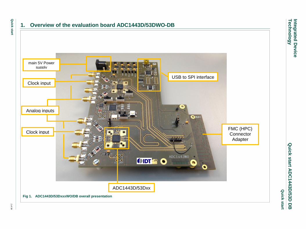
1. Overview of the evaluation board ADC1443D/53DWO-DB
Fig 1. ADC1443D/53DxxxWO/DB overall presentation
Analog inputs
Clock input
main 5V Power supply
USB to SPI interface
FMC (HPC) Connector Adapter
ADC1443D/53Dxxx
Clock input

Inte
gra
ted
De
vic
e
Tec
hn
olo
gy
Qu
ick s
tart
Qu
ick
sta
rt AD
C14
43D
/53
D D
B
Qu
ick s
tart
3 o
f 39
2. Switch and Jumpers default state
Fig 2. Overall presentation of default switches and jumpers
Scrambler off
Ext clock
3.3V
Integrated Device Technology Quick start ADC1443D/53D DB
.
Quick start IV
3. Board goal and general description
The ADC1443D/53DxxxWO/DB board along with Xilinx KC705 development board are
aimed to provide a full and complete set to evaluate and demonstrate the
ADC1x43D/53D series, analog to digital converters, compliant with JESD204B JEDEC
serialization standard.
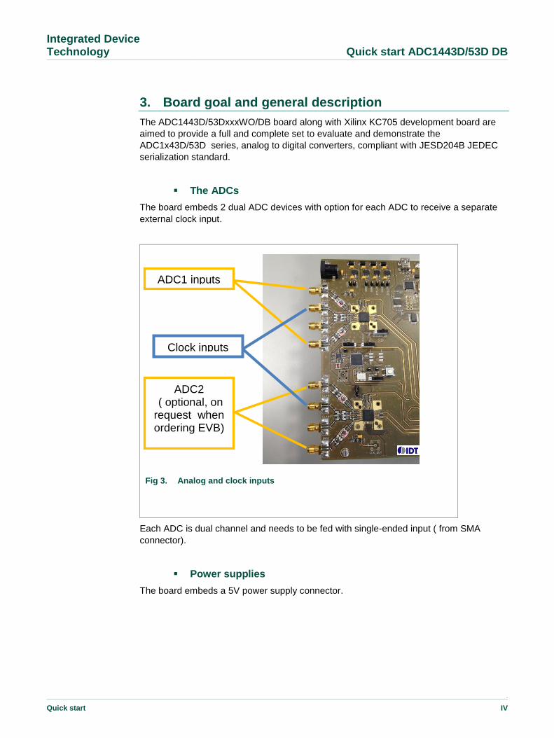
The ADCs
The board embeds 2 dual ADC devices with option for each ADC to receive a separate
external clock input.
Fig 3. Analog and clock inputs
Each ADC is dual channel and needs to be fed with single-ended input ( from SMA
connector).
Power supplies
The board embeds a 5V power supply connector.
ADC1 inputs
ADC2 ( optional, on request when ordering EVB)
Clock inputs

Integrated Device Technology Quick start ADC1443D/53D DB
.
Quick start V
Fig 4. 5V DC power connector
Downloading the FPGA bit file
The FPGA code, in the form of a bit file, requires to be downloaded via the KC705
external JTAG connector.
Fig 5. Xilinx KC705 JTAG connector
To download the Kintex-7 bit file, ISE Design Suite 13.3 or later is required from Xilinx, or
at a minimum the Xilinx ChipeScope Pro 64-bit version tool.
The FPGA is responsible for de-serializing the serial stream coming From the ADC,
according to the JESD204B standard.
Integrated Device Technology Quick start ADC1443D/53D DB
.
Quick start VI
Since we have 2 dual ADC on the board, each with 2 lanes, the HSDC_SW_ADC_4.exe
application allows to configure the FPGA and to choose which channel, ADC, lanes we
want to acquire.
The FPGA is accessible via the same USB-to-SPI interface on the ADC board.
Fig 6. USB-to-SPI interface
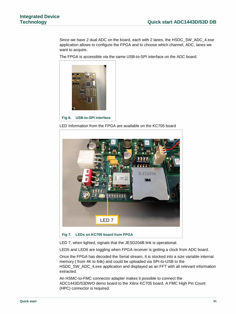
LED Information from the FPGA are available on the KC705 board
Fig 7. LEDs on KC705 board from FPGA
LED 7, when lighted, signals that the JESD204B link is operational.
LED5 and LED6 are toggling when FPGA receiver is getting a clock from ADC board.
Once the FPGA has decoded the Serial stream, It is stocked into a size variable internal
memory ( from 4K to 64k) and could be uploaded via SPI-to-USB to the
HSDC_SW_ADC_4.exe application and displayed as an FFT with all relevant information
extracted.
An HSMC-to-FMC connector adapter makes it possible to connect the
ADC1443D/53DWO demo board to the Xilinx KC705 board. A FMC High Pin Count
(HPC) connector is required.
LED 7
Integrated Device Technology Quick start ADC1443D/53D DB
.
Quick start VII
Fig 8. HSMC-to-FMC connector adapter (HSMC side shown) for
connection to Xilinx KC705 board
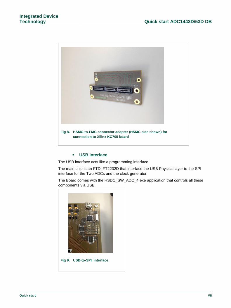
USB interface
The USB interface acts like a programming interface.
The main chip is an FTDI FT2232D that interface the USB Physical layer to the SPI
interface for the Two ADCs and the clock generator.
The Board comes with the HSDC_SW_ADC_4.exe application that controls all these
components via USB.
Fig 9. USB-to-SPI interface

Integrated Device Technology Quick start ADC1443D/53D DB
.
Quick start VIII
Further instructions on how to install and operate the software are detailed in next
section.
4. Software and drivers install
4.1 Labview Runtime 2010 install
1 Go to National Instruments web page http://joule.ni.com/nidu/cds/view/p/id/2087/lang/en
2 Download
‘LVRTE2010std.exe’
3 Save
4 Run the application ‘LVRTE2010std.exe’
5 OK

Integrated Device Technology Quick start ADC1443D/53D DB
.
Quick start IX
6 Unzip
7 OK
8 Next
9 Next

Integrated Device Technology Quick start ADC1443D/53D DB
.
Quick start X
10 Next
11 Select ‘I accept the License
Agreement’
Next
12 Next
Integrated Device Technology Quick start ADC1443D/53D DB
.
Quick start XI
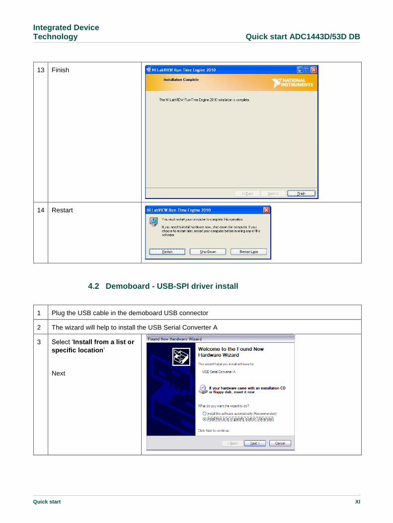
13 Finish
14 Restart
4.2 Demoboard - USB-SPI driver install
1 Plug the USB cable in the demoboard USB connector
2 The wizard will help to install the USB Serial Converter A
3 Select ‘Install from a list or
specific location’
Next

Integrated Device Technology Quick start ADC1443D/53D DB
.
Quick start XII
4 Select ‘Search for the best
driver in these locations’
Select ‘Include this location
in the search’
Browse
Select the folder
‘CDM2.08.12’
Next
5 Continue Anyway
(Windows XP only)
6 Browse
Select the file ‘ftdibus.sys’
in the folder
‘CDM2.08.12\i386’
OK

Integrated Device Technology Quick start ADC1443D/53D DB
.
Quick start XIII
7 Finish
8 The wizard will help to install the USB Serial Converter B (same as USB Serial Converter A)
9 The wizard will help to install the USB serial port
The file ‘ftser2k.sys’ is in the folder ‘CDM2.08.12\i386’

Integrated Device Technology Quick start ADC1443D/53D DB
Quick start 14 of 39
5. ADC1443D/53DWO + Xilinx KC705 demo setup
5.1 Connecting ADC1443D/53DxxxWO and KC705 boards
To attach the ADC1443D/53DxxxWO board to the Xilinx KC705 board. Refer to Fig 10:
1. attach the HSMC-to-FMC adapter to the ADC1443DxxxWO demo board;
2. then attach the combined ADC1443 board and adapter to the FMC HPC (High Pin
Count) connector of the KC705 board;
3. it is recommended to prop-up the feet of the ADC board to make it stable and level;
4. connect an external clock signal to CLKP1 SMA connector (for example 153.6 MHz
at +15 dBm level);
5. connect the external input signal to INA1 and/or INB1 SMA connector (for example
170 MHz at +10 dBm level);
6. it is recommended for best dynamic performance to use an in-line external bandpass
filter for the external input signal;
7. it is recommended, in order to support “coherent sampling”, that the external clock
and input signal generators be frequency locked (i.e. the “external ref out” of one is
connected to the “external ref in” of the other).
Fig 10. ADC1443D/53DxxxWO demo board + Xilinx KC705 board setup
Ext CLK
Input Signal
Input Signal and CLK sources should be frequency locked
Integrated Device Technology Quick start ADC1443D/53D DB
Quick start 15 of 39
5.2 KC705 board start-up
It is highly recommended that the KC705 board be started before the
ADC1443D/53DWO board. This is to help ensure a consistent startup process:
make sure that the ADC1443D/53DxxxWO board USB and DC power cables are
disconnected;
connect the USB-JTAG and DC power cables to the KC705 board.
ensure that the KC705 power switch is in the “on” position;
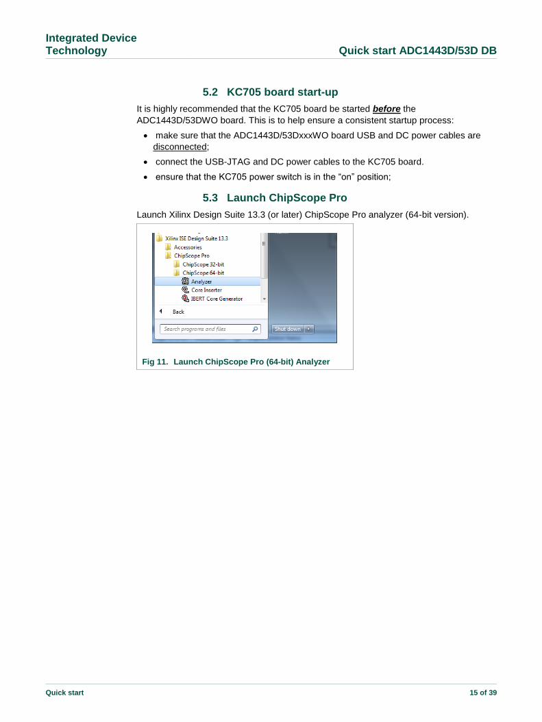
5.3 Launch ChipScope Pro
Launch Xilinx Design Suite 13.3 (or later) ChipScope Pro analyzer (64-bit version).
Fig 11. Launch ChipScope Pro (64-bit) Analyzer

Integrated Device Technology Quick start ADC1443D/53D DB
Quick start 16 of 39
Perform search of JTAG chain.
Fig 12. ChipScope Pro start-up screen
Click “OK” to close pop-up window.
Fig 13. Click “OK”
Click icon to start JTAG search
Click OK
Integrated Device Technology Quick start ADC1443D/53D DB
Quick start 17 of 39
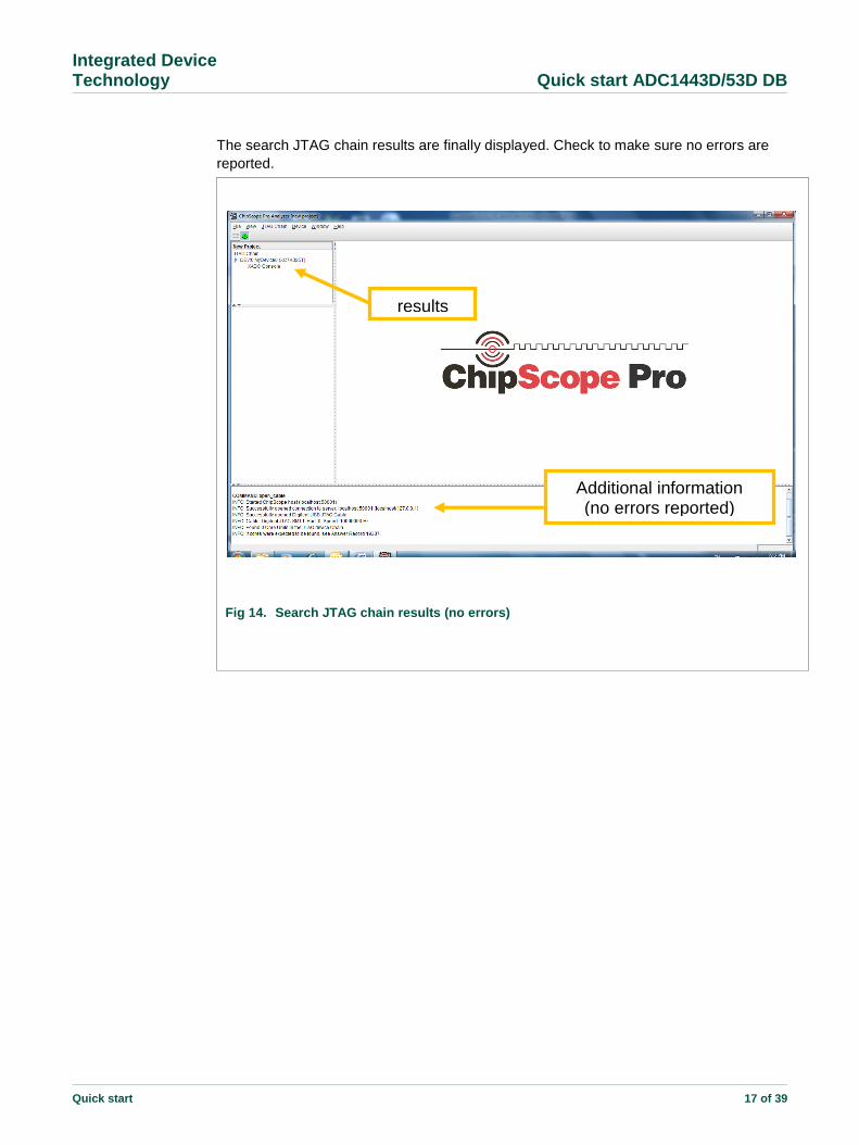
The search JTAG chain results are finally displayed. Check to make sure no errors are
reported.
Fig 14. Search JTAG chain results (no errors)
Additional information (no errors reported)
results

Integrated Device Technology Quick start ADC1443D/53D DB
Quick start 18 of 39
5.4 Download Kintex-7 FPGA bit file
Downloading the Kintex-7 bit file requires use of the ChipScope Pro tool.
Go to the “Device” tab to configure the path where the bit file is located on your hard
drive.
Fig 15. Configure path of FPGA bit file
Configure path of bit file
Integrated Device Technology Quick start ADC1443D/53D DB
Quick start 19 of 39
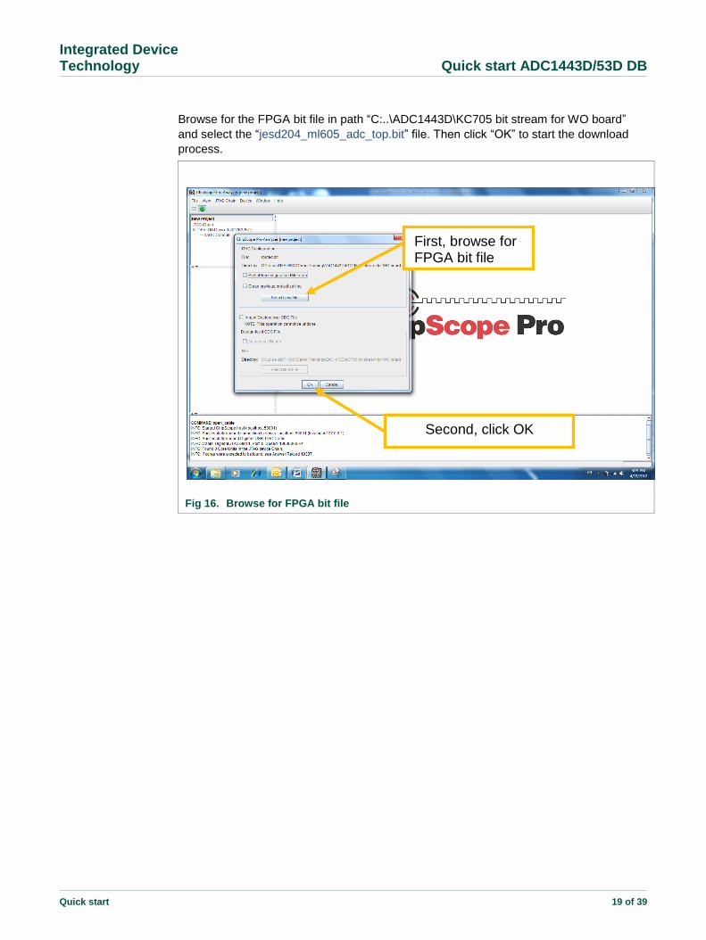
Browse for the FPGA bit file in path “C:..\ADC1443D\KC705 bit stream for WO board”
and select the “jesd204_ml605_adc_top.bit” file. Then click “OK” to start the download
process.
Fig 16. Browse for FPGA bit file
First, browse for FPGA bit file
Second, click OK
Integrated Device Technology Quick start ADC1443D/53D DB
Quick start 20 of 39
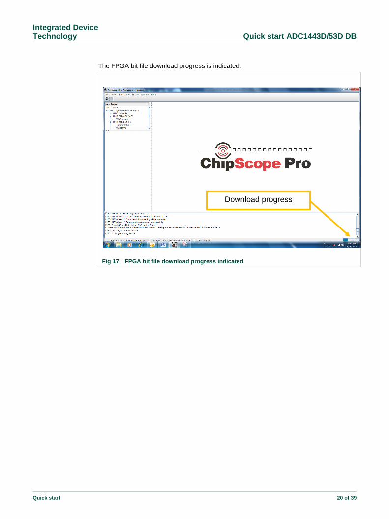
The FPGA bit file download progress is indicated.
Fig 17. FPGA bit file download progress indicated
Download progress

Integrated Device Technology Quick start ADC1443D/53D DB
Quick start 21 of 39
5.5 ADC1443D/53DxxxWO board start-up
It is highly recommended that the KC705 board be started before the
ADC1443D/53DWO board. This is to help ensure a consistent startup process:
make sure that the KC705 board is powered and the FPGA bit file is downloaded
(sections 5.1 - 5.4);
connect the USB cable (first) and DC power cable to the ADC1443D/53DWO board;
check to make sure green LEDs are lighted on the ADC1443D/53DWO board;
Fig 18. Check that ADC1443D/53DWO green LEDs are lighted
Check green LEDs lighted

Integrated Device Technology Quick start ADC1443D/53D DB
Quick start 22 of 39
check to make sure green LEDs are toggling on the KC705 board;
Fig 19. Check that KC705 green LEDs toggle
Check green LEDs toggle

Integrated Device Technology Quick start ADC1443D/53D DB
Quick start 23 of 39
5.6 Launch ADC1443 GUI
Run the application “HSDC_SW_ADC_4.exe”.
Configure the settings as appropriate for application per Fig 20 below.
Fig 20. ADC1443D GUI start-up screen
Select the wanted product e.g : ADC1443D125 Select ‘Coherent’ for
optimized FFT processing. Otherwise select ‘Not coherent’
Select the number of points for FFT
Enter the sampling frequency
Enter the input frequency. The coherent frequency will be automatically calculated (to be entered on external signal generator)
Select host board type
Integrated Device Technology Quick start ADC1443D/53D DB
Quick start 24 of 39
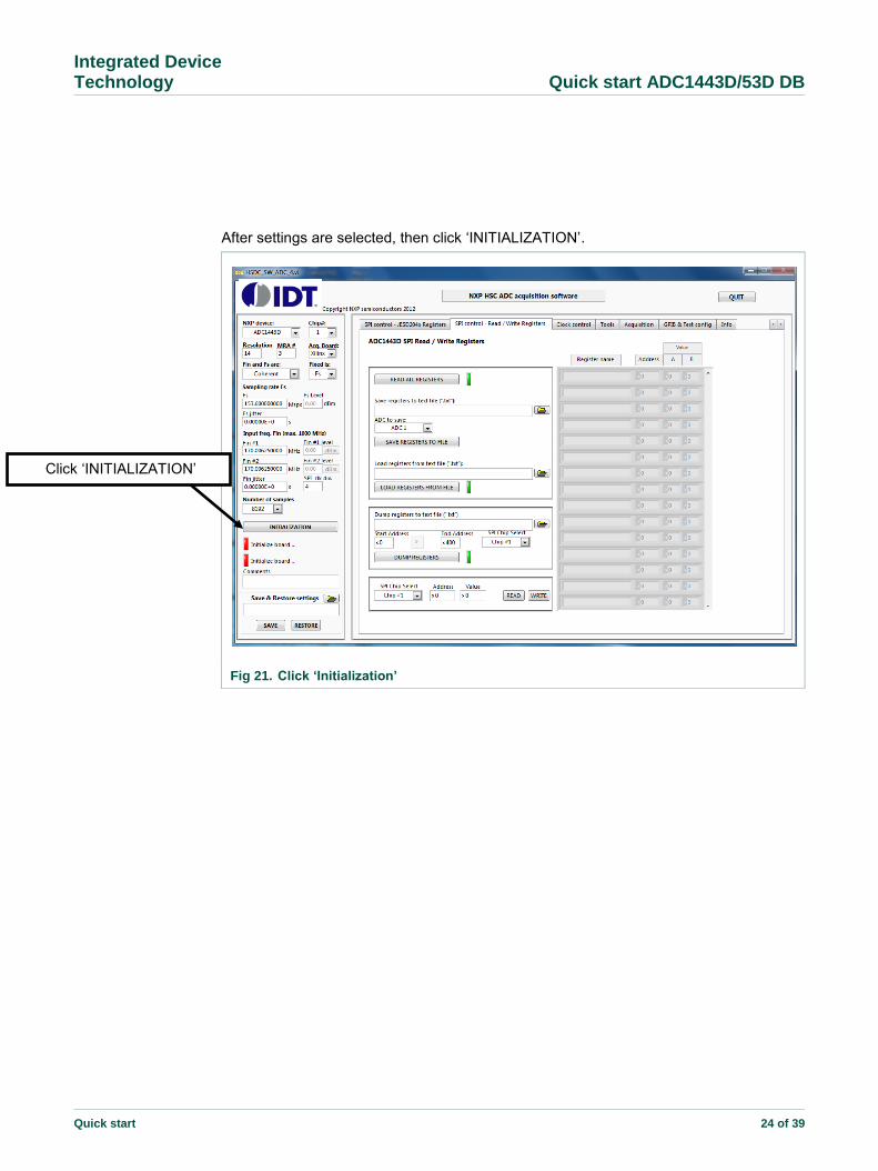
After settings are selected, then click ‘INITIALIZATION’.
Fig 21. Click ‘Initialization’
Click ‘INITIALIZATION’

Integrated Device Technology Quick start ADC1443D/53D DB
Quick start 25 of 39
Check ‘green’ LED indicators.
Fig 22. Check green LED indicators
‘GREEN’ when ADC1443 board USB is ready
‘GREEN’ when host acquisition board USB is ready

Integrated Device Technology Quick start ADC1443D/53D DB
Quick start 26 of 39
5.7 Download ADC1443 configuration file
Download the ADC1443 configuration file. This file configures the JESD204B internal
registers.
In the field ‘Load registers from text file (“.txt”)’, browse and select the appropriate file
Example: “ADC1453D_ 250Msps_SPI_C.txt”.
Then click ‘LOAD REGISTERS FROM FILE’ button.
Fig 23. ADC1443 GUI start-up screen
Second, click ‘LOAD REGISTERS FROM FILE’
First, browse for the ADC1443 configuration file
Integrated Device Technology Quick start ADC1443D/53D DB
Quick start 27 of 39
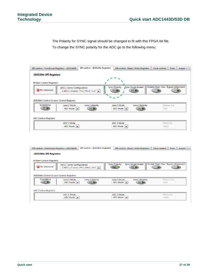
The Polarity for SYNC signal should be changed to fit with this FPGA bit file.
To change the SYNC polarity for the ADC go to the following menu:

Integrated Device Technology Quick start ADC1443D/53D DB
Quick start 28 of 39
5.8 Load ChipScope Pro project
Using the ChipScope Pro tool, load the FPGA project file. This will enable debugging
capabilities.
Go to the “File” tab to open the project:
Fig 24. Open project start
Select ‘No’, to not save any changes.
Fig 25. Select ‘No’
Go to File tab, Open Project
Click ‘No’

Integrated Device Technology Quick start ADC1443D/53D DB
Quick start 29 of 39
Browse for the FPGA project file and select the “chipscope3.cpj” file. The FPGA project is
loaded with the following screen in Fig 26.
Fig 26. FPGA project screen

Integrated Device Technology Quick start ADC1443D/53D DB
Quick start 30 of 39
5.9 Force a FPGA JESD204B link reset
A forced FPGA JESD204B link reset is required in order to enable initial data acquisition.
First, click on the “VIO Console” so that its corresponding window appears in the
foreground.
Second, click on the ‘reset’ field value ‘0’, so that it momentarily toggles to a ‘1’. This
performs a reset for the FPGA JESD204B.
Fig 27. Force FPGA JESD204B reset
Writing 22 to address 0 , launch the sysref and allow the system to have a deterministic
latency.
After the reset is performed, check that the LED on the KC705 board is lighted
Now you could use the Labview interface to capture using the external signal as a tigger.
First, click “VIO Console”
Second, click on ‘0’ to toggle it to a ‘1’ momentarily
third, set the Address to 0. Set the Write_data to “00000022” Hit write

Integrated Device Technology Quick start ADC1443D/53D DB
Quick start 31 of 39
Fig 28. Check that KC705 green LED is lighted (last one on the left)
5.10 View internal FPGA waveform result
After the forced FPGA JESD204B link reset has been issued, view the reconstructed
waveform to make sure that a good JESD204B link is established.
First, click on the “Bus Plot” so that it’s corresponding window appears in the foreground.
Second, select ‘sine0’ if viewing JESD204B lane corresponding to INB input of the ADC,
and select ‘sine1’ if viewing JESD204B lane corresponding to INA input of the ADC.
Third, click on the ‘T!’ field to create a data trigger.
Fig 29. View internal FPGA waveform result
Check green LED is lighted
First, click “Bus Plot”
Third, click on ‘T!’ to create data trigger
Waveform result is displayed
Second, ‘sine0’ corresponds to INB input of ADC, and ‘sine1’ corresponds to INA input of ADC

Integrated Device Technology Quick start ADC1443D/53D DB
Quick start 32 of 39
If waveform result looks bad, or is not as expected, then repeat FPGA JESD204B
link reset explained in previous section 5.9. And then click “T!” afterwards to view
new waveform result.

Integrated Device Technology Quick start ADC1443D/53D DB
Quick start 33 of 39
5.1 Using ADC1443D/53D GUI to acquire data
After the forced FPGA JESD204B link reset has been issued, and the FPGA
reconstructed waveform is confirmed to look as expected, then the ADC1443 GUI can be
used henceforth to continuously acquire data and display and store results.
on the Acquisition tab, you could hit the save samples and specify a path to get the data
on a text file.
Choose Display# 1 on the scroll menu
And finally hit acquire to get the data
Under Reorganized Signal and Unreconstructed Signal Sub-Tab, you have the Sinwave
temporal view
Select Display#1
Save samples & path Acquire
Integrated Device Technology Quick start ADC1443D/53D DB
Quick start 34 of 39
6. Other notes on ADC1443D/53D GUI
6.1 Software start-up
The ADC1443D/53D GUI applicaton will allow:
the user to control features through the SPI;
as well as performing any online data acquisition to evaluate the performances.
6.2 Read / Write Registers
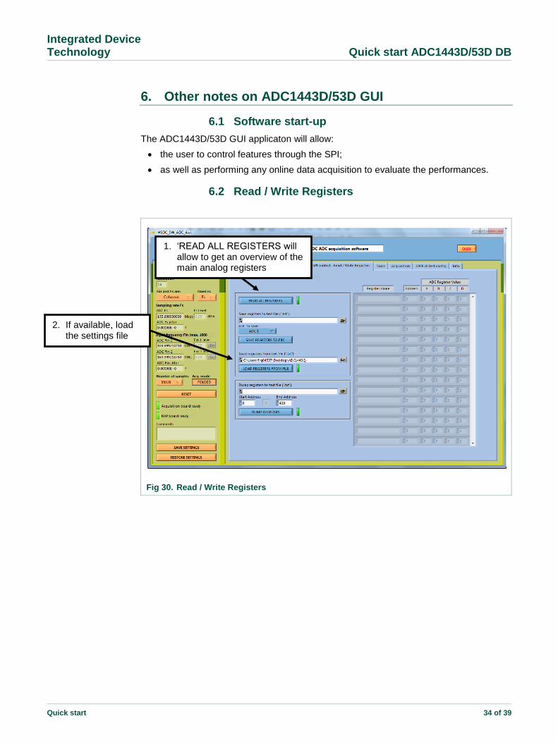
Fig 30. Read / Write Registers
1. ‘READ ALL REGISTERS will allow to get an overview of the main analog registers
2. If available, load the settings file

Integrated Device Technology Quick start ADC1443D/53D DB
Quick start 35 of 39
6.3 Functional Registers
Fig 31. Functional Registers
1. Select the channels to be modified
2. ‘Write all registers’ allow to send all the values at the same time
3. Write the value in the register
4. Modify the value

Integrated Device Technology Quick start ADC1443D/53D DB
Quick start 36 of 39
6.4 Acquisition
Fig 32. Acquisition
2. If ‘Not coherent’, select a window for procesing
1. If needed, the performances can be calculated over a reduced bandwidth
6. Performances are available in the table
3. Click acquire to process data acquisition and FFT processing
4. Select ‘Continuous acquisition’ for real-time processing
5. Select the channel to display
Integrated Device Technology Quick start ADC1443D/53D DB
Quick start 37 of 39
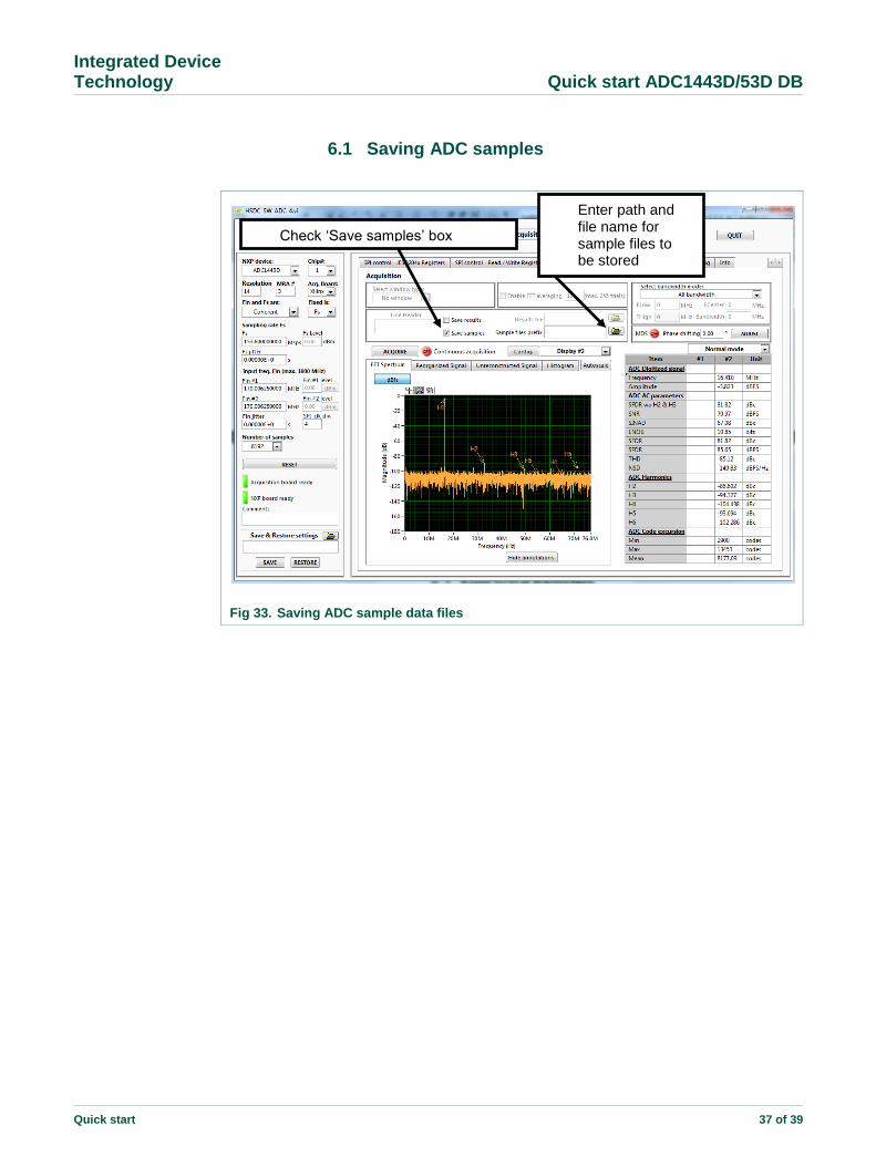
6.1 Saving ADC samples
Fig 33. Saving ADC sample data files
Check ‘Save samples’ box
Enter path and file name for sample files to be stored

Integrated Device Technology Quick start ADC1443D/53D DB
Quick start 38 of 39
7. ADC EVB HSMC connector pinout

Integrated Device Technology Quick start ADC1443D/53D DB
Quick start 39 of 39
8. HSMC-FMC adaptor board pinout