euv mask inspection: a bright idea? - blue sky...
TRANSCRIPT

EUV mask inspection:a bright idea?EUV mask inspection:a bright idea?
Kenneth A. Goldberg, Ph.D.Lawrence Berkeley National Laboratory
Wailea, Maui, Hawaii, June 12, 2008
http://Goldberg.LBL.gov
Kenneth A. Goldberg, Ph.D.Lawrence Berkeley National Laboratory
Wailea, Maui, Hawaii, June 12, 2008
http://Goldberg.LBL.gov

Kenneth A. Goldberg, Ph.D.Lawrence Berkeley National Laboratory
Wailea, Maui, Hawaii, June 12, 2008
Kenneth A. Goldberg, Ph.D.Lawrence Berkeley National Laboratory
Wailea, Maui, Hawaii, June 12, 2008
EUV mask inspection:a bright idea?EUV mask inspection:a bright idea?


Different wavelengths see the same ML structure differently
λ“1%” depth
bi- layers
13.4 nm 215 nm 31488 nm 53.6 nm 8266 nm 20.6 nm 3
EUV light penetrates deeply into the resonant ML structure.488-nm and 266-nm light barely reaches below the surface.EUV light penetrates deeply into the resonant ML structure.488-nm and 266-nm light barely reaches below the surface.
Field Penetration for three λs
0.01
1.00
depth [nm]
Field intensity vs. depth
At-wavelength testing probes the actual multilayer response.

• colorblind inspection: more than skin deep• modeling: size does matter• Lasertec M7360: detectability• actinic imaging: seeing is believing• EUV brightfield defect detection: Yes, we can
Outline
d=“SEVd” =Spherical EquivalentVolume diameter


M7360-detectable defects > 29 nm SEVd
K J I H G F E D C B A
0.9 2.4 height
39.1 48.8 FWHML
Wonil Cho, SPIE 6730
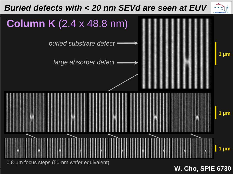
buried substrate defect
1 µm
1 µm
1 µm
0.8-µm focus steps (50-nm wafer equivalent)
large absorber defect
Column K (2.4 x 48.8 nm)Buried defects with < 20 nm SEVd are seen at EUV
W. Cho, SPIE 6730

buried substrate defect
1 µm
1 µm
1 µm
0.8-µm focus steps (50-nm wafer equivalent)
large absorber defect
Column L (0.9 x 38.1 nm)Buried defects with < 15 nm SEVd are seen at EUV
W. Cho, SPIE 6730

Printability vs. Detectability Summaryhe
ight
(nm
)
Good News!Actinic imaging:Small defects are Less Printable than predicted
Bad NewsM7360 did not detect
critical defects for 40 nm HP
W. Cho, SPIE 6730

How long would it take to scan an EUV mask with EUV light?
Consider an EUV mask-blank inspection tool
Defect Size Source PowerStatistics
Result
Beam Size
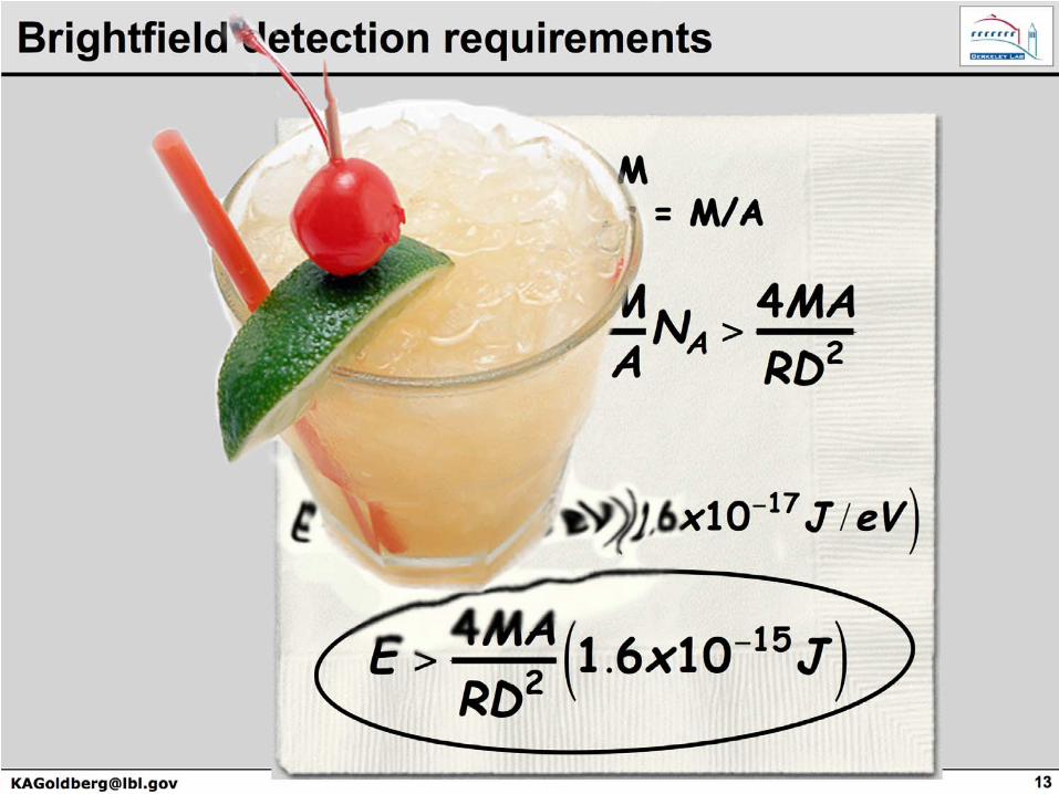
Remember:• In Brightfield you look for tiny changes in R.• In Darkfield you search for scattering, BUT
you can miss large dark defects completely!

Total mask area, MNumber of patches = M/A
MA
NA > 4MARD2
Total Number of photons
Total Energy
E > 4MA
RD2 100 eV( )1.6x10⁻¹⁷J /eV( )
E > 4MA
RD2 1.6x10⁻¹⁵J( )
To detect the change we need
N > 2A
D⎛
⎝ ⎜
⎞
⎠ ⎟ 2
Reflectivity is R.Assume Q.E. = 100%
1N
< D2A
or
NA > 1
R2AD
⎛
⎝ ⎜
⎞
⎠ ⎟ 2
in each patch A
Brightfield detection requirements
A D
Reflected Intensity relative change DA
Measure N photons,relative uncertainty
NN
= 1N
N

Total mask area, MNumber of patches = M/A
MA
NA > 4MARD2
Total Number of photons
Total Energy
E > 4MA
RD2 100 eV( )1.6x10⁻¹⁷J /eV( )
E > 4MA
RD2 1.6x10⁻¹⁵J( )
Brightfield detection requirements
To detect the change we need
N > 2A
D⎛
⎝ ⎜
⎞
⎠ ⎟ 2
Reflectivity is R.Assume Q.E. = 100%
1N
< D2A
or
NA > 1
R2AD
⎛
⎝ ⎜
⎞
⎠ ⎟ 2illuminating
each patch, A

Brightfield detection requirements
Total mask area, MNumber of patches = M/A
MA
NA > 4MARD2
Total Number of photons
Total Energy
E > 4MA
RD2 100 eV( )1.6x10⁻¹⁹J /eV( )
E > 4MA
RD2 1.6x10⁻¹⁷J( )Note: This slide has been corrected.The original slide, had an errorin the exponent here.
Brightfield detection requirements
Total mask area, MNumber of patches = M/A
MA
NA > 4MARD2
Total Number of photons
Total Energy
E > 4MA
RD2 100 eV( )1.6x10⁻¹⁷J /eV( )
E > 4MA
RD2 1.6x10⁻¹⁵J( )

R = 60%, M = (100 mm)2
D =A [µm] 40 nm 30 nm 20 nm 10 nm
10 42 132 667 106675 10 33 167 2667 Einc [J]1 0.4 1 6.7 107
0.5 0.1 0.3 1.7 27
incident EUV energy
Each case is < 1h with a 10W (IF) sourceand a 30% efficient illuminator.
E > 4MA
RD2 1.6x10⁻¹⁵J( )
EUV mask-blank scanning: It can be done
3h @ 1W

Will lowly defects stop EUVL?
defectdefect defectdefectdefect defect
EUVL?EUVL?

Will lowly defects stop EUVL?
defectdefect defectdefectdefect defect
MaskInspection!
MaskInspection!EUVL?EUVL?
Not if it’sour move!