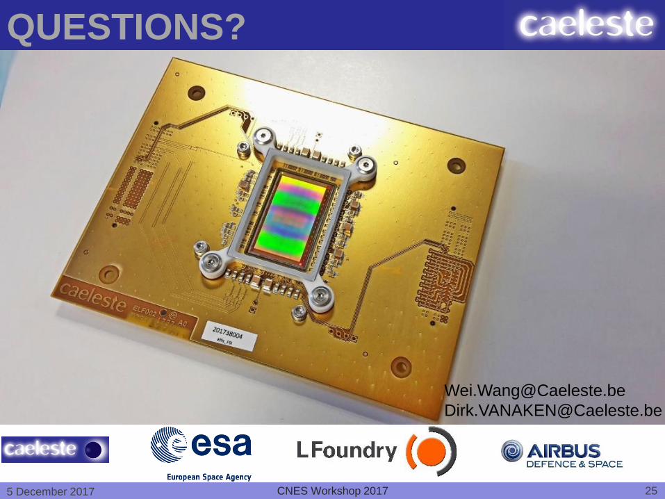
european low flux cmos image sensor - caeleste
TRANSCRIPT
European Low Flux CMOS Image Sensor
Description and Preliminary Results
Ajit Kumar Kalgi1, Wei Wang1, Bart Dierickx1, Dirk Van Aken1, Kaiyuan Wu1,
Alexander Klekachev1, Gerlinde Ruttens1, Kyriaki Minoglou2, Franz Riedlberger3,
Giuseppe Di Nicolantonio3, Francesco Palumbi3, Alice Pelamatti4
3 421
25 December 2017
Outline
• Introduction
• The ELFIS project
• Need for charge domain Global Shutter (GS), High
Dynamic Range(HDR) imaging
• The ELFIS image sensor
• Sensor Floorplan
• Target specifications and features
• Charge domain GS HDR Pixel operation
• Test Setup
• First Image
• Conclusions
CNES Workshop 2017

35 December 2017
Project Description
▪ ESA funded project “European Low Flux CMOS Image
Sensor”
▪ Goal: to develop a Radiation hard, charge domain global
shutter, high dynamic range pixel for low flux / high flux
space applications
▪ Project Partners
▪ LFOUNDRY: GS process development, wafer processing,
backside thinning.
▪ AIRBUS: Electro optical characterization at 173K
▪ Project duration: 30 months
▪ Start: Feb 2016
▪ End: August 2018
▪ Project status: FSI Silicon
CNES Workshop 2017
45 December 2017
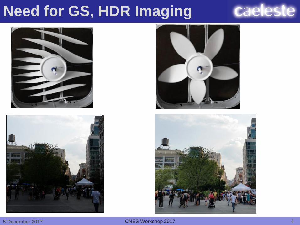
Need for GS, HDR Imaging
CNES Workshop 2017
55 December 2017
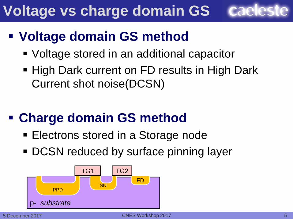
Voltage vs charge domain GS
▪ Voltage domain GS method
▪ Voltage stored in an additional capacitor
▪ High Dark current on FD results in High Dark
Current shot noise(DCSN)
▪ Charge domain GS method
▪ Electrons stored in a Storage node
▪ DCSN reduced by surface pinning layer
CNES Workshop 2017
p- substrate
SNFD
PPD
TG2TG1

65 December 2017
Outline
• Introduction
• The ELFIS project
• Need for True Global Shutter (GS), High Dynamic
Range(HDR) imaging
• The ELFIS image sensor
• Sensor Floorplan
• Target specifications and features
• Charge domain GS HDR Pixel operation
• Test Setup
• First Image
• Conclusions
CNES Workshop 2017
75 December 2017
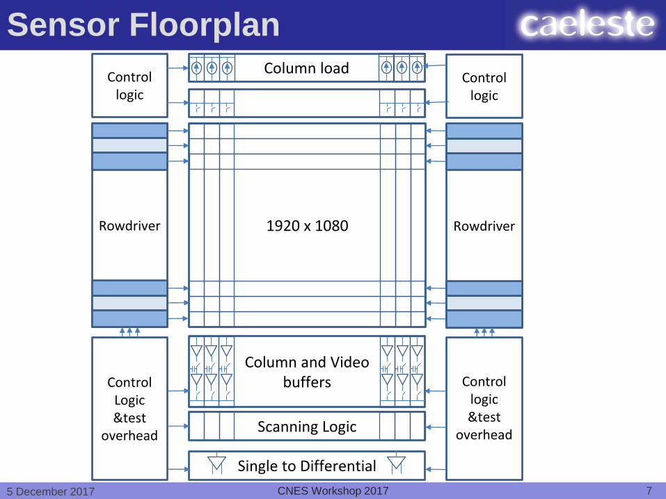
Sensor Floorplan
CNES Workshop 2017
1920 x 1080Rowdriver Rowdriver
Column load
Column and Video buffers
Scanning Logic
Single to Differential
Control logic
Control Logic&test
overhead
Control logic&test
overhead
Control logic

85 December 2017
Pixel Specifications
CNES Workshop 2017
Process Lfoundry 110nm CMOS Image Sensor
Pixel size 15µm x 15µm
Pixel array 1920 x 1080
Full WellHigh Gain: 7Ke-
Low Gain: 200Ke-
Read Noise
High Gain: 5e-(nominal condition)
High Gain: 2.5e-(low noise mode)
Low Gain: 110e-
Shutter Mode
Rolling Shutter
Integrate then Read(ITR)
Integrate While Read(IWR)
Fill Factor 100%
CIS Type Backside Illuminated
Quantum Efficiency>50% 350nm – 800nm
>90% peak
MTF >50% @ 1 Nyquist
Dark Current < 50 e/s/pixel @ 25°C

95 December 2017
Other Specifications
CNES Workshop 2017
CDS Programmable on or off-chip CDS
Frame rate 75 FPS @ GS HDR
Clock Speed 40MHz
Output Channels 16
Power Consumption 700mW
TID 100KRad
SEL 62 MeV.cm2/mg
Operating Temperature -100°C - +60°C
Packaging COB
Stitch design Stitchable up to wafer scale

105 December 2017
GS HDR Pixel - Topology
CNES Workshop 2017
• High Gain: TG1 - SN - TG2
• Low Gain-a: TG3a - Ca - Ma
• Low Gain-b: TG3b - Cb - Mb
• Low Gain-a, Low Gain-b are
used for IWR operation
HG
LG
LG
p-
SNFD
PPD
CN
C
TG2TG3 TG1

115 December 2017
GS HDR Pixel - layout
CNES Workshop 2017
PPD
TG1
TG2
SN
FD
TG3
C
RESET
VDD
Output:
Reset Signal,
High Gain signal,
Low Gain Signal
125 December 2017
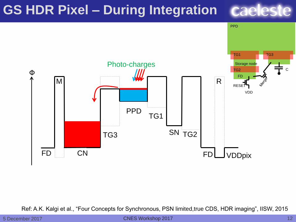
GS HDR Pixel – During Integration
CNES Workshop 2017
ФPhoto-charges
FD
PPD
TG3
CN
M R
FD VDDpix
SN
TG1
TG2
Ref: A.K. Kalgi et al., “Four Concepts for Synchronous, PSN limited,true CDS, HDR imaging”, IISW, 2015
PPD
TG1
TG2
Storage node
FD
TG3
C
RESET
VDD
135 December 2017
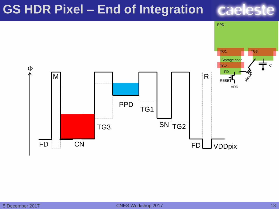
GS HDR Pixel – End of Integration
CNES Workshop 2017
PPD
TG3
CN FD VDDpix
SN
TG1
TG2
FD
ФM R
PPD
TG1
TG2
Storage node
FD
TG3
C
RESET
VDD

145 December 2017
GS HDR Pixel – PPD to SN
CNES Workshop 2017
PPD
TG3
FD VDDpix
SN
TG1
TG2
FD
Ф
CN
M R
PPD
TG1
TG2
Storage node
FD
TG3
C
RESET
VDD

155 December 2017
GS HDR Pixel – Next Integration
CNES Workshop 2017
PPD
TG3
FD VDDpix
SN
TG1
TG2
Next
tint
FD
Ф
CN
M R
PPD
TG1
TG2
Storage node
FD
TG3
C
RESET
VDD

165 December 2017
GS HDR Pixel – Reset Readout
CNES Workshop 2017
PPD
TG3
FD VDDpix
SN
TG1
TG2
output
Select
“R1”
Next
tint
FD
Ф
CN
M R
PPD
TG1
TG2
Storage node
FD
TG3
C
RESET
VDD

175 December 2017
GS HDR Pixel –SN to FD
CNES Workshop 2017
PPD
TG3
FD VDDpix
SN
TG1
TG2
Next
tint
FD
Ф
CN
M R
PPD
TG1
TG2
Storage node
FD
TG3
C
RESET
VDD
185 December 2017
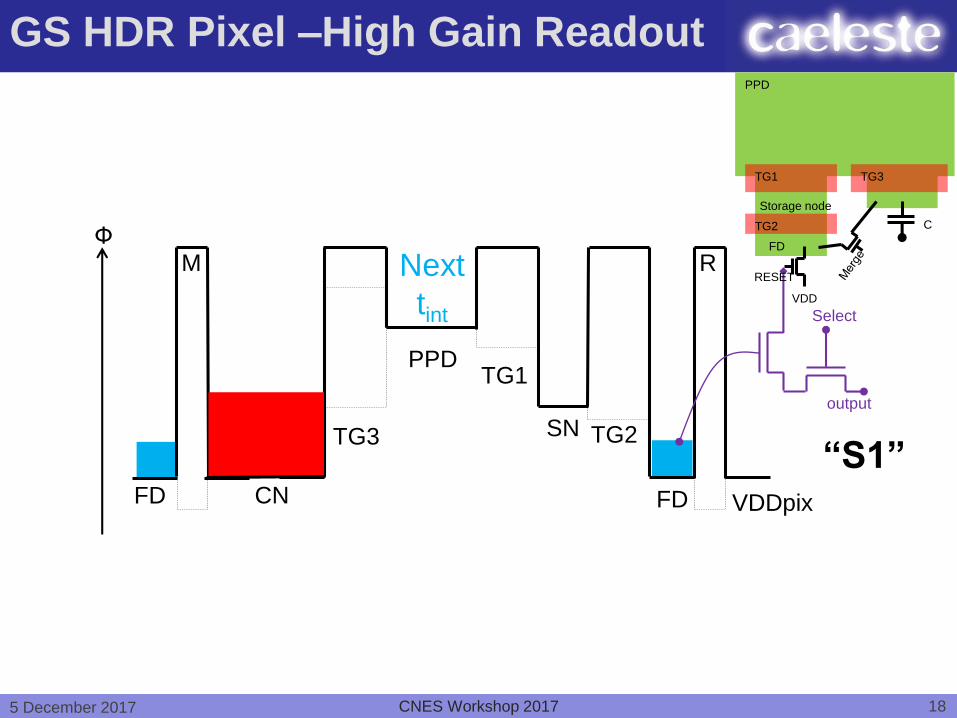
GS HDR Pixel –High Gain Readout
CNES Workshop 2017
PPD
TG3
FD VDDpix
SN
TG1
TG2
output
Select
Next
tint
FD
Ф
CN
M R
PPD
TG1
TG2
Storage node
FD
TG3
C
RESET
VDD
“S1”
195 December 2017
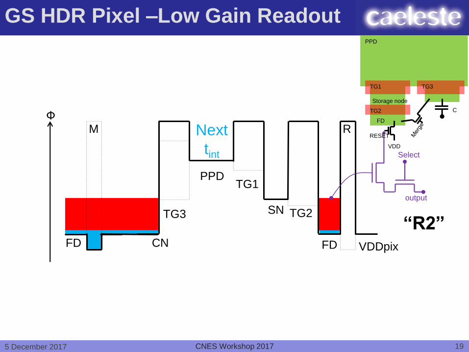
GS HDR Pixel –Low Gain Readout
CNES Workshop 2017
PPD
TG3
FD VDDpix
SN
TG1
TG2
output
Select
Next
tint
FD
Ф
CN
M R
PPD
TG1
TG2
Storage node
FD
TG3
C
RESET
VDD
“R2”

205 December 2017
Outline
• Introduction
• The ELFIS project
• Need for True Global Shutter (GS), High Dynamic
Range(HDR) imaging
• The ELFIS image sensor
• Sensor Floorplan
• Target specifications and features
• Charge domain GS HDR Pixel operation
• Test Setup
• First Image
• Conclusions
CNES Workshop 2017
215 December 2017
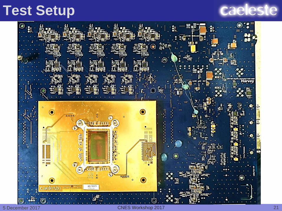
Test Setup
CNES Workshop 2017
225 December 2017
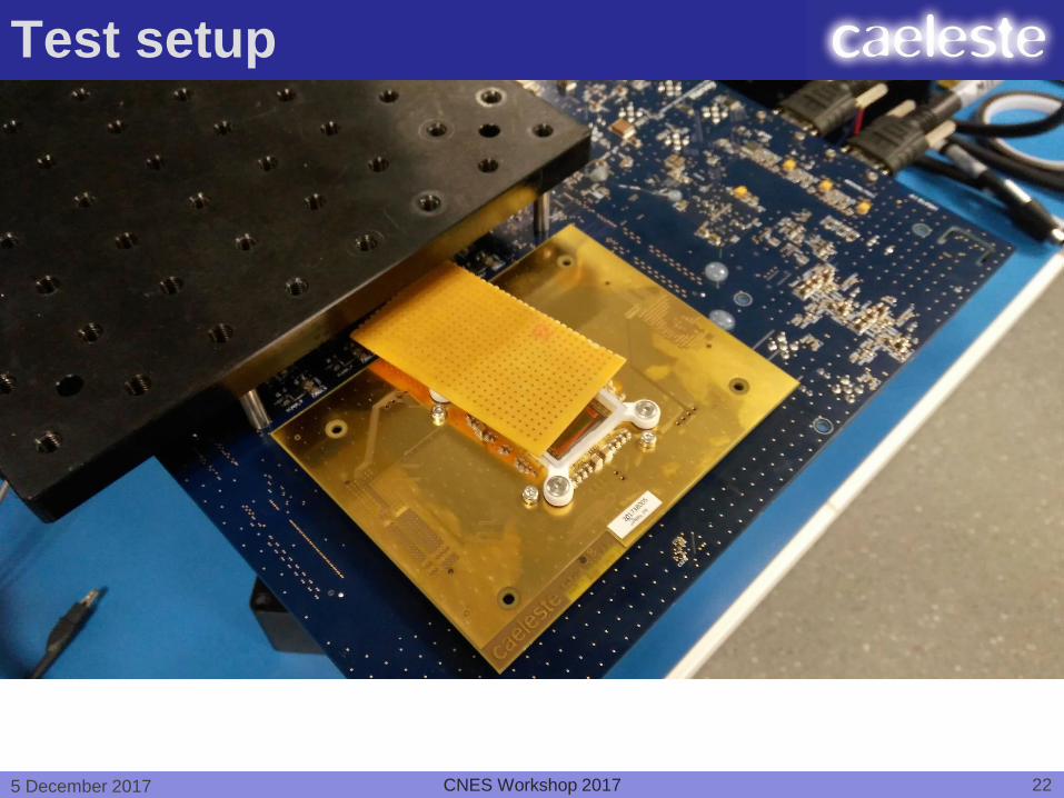
Test setup
CNES Workshop 2017

235 December 2017
FIRST IMAGE
CNES Workshop 2017
Operation mode: Global Shutter, High Gain

245 December 2017
Conclusions
• First preliminary result with New Charge
domain GS process
• Fully European supply chain
• True GS, fully synchronous HDR pixel is
realized for various process conditions
• Future work
• GS Process evaluation by various process splits
• Finishing BSI wafers
CNES Workshop 2017

265 December 2017
Backup slides
CNES Workshop 2017
275 December 2017
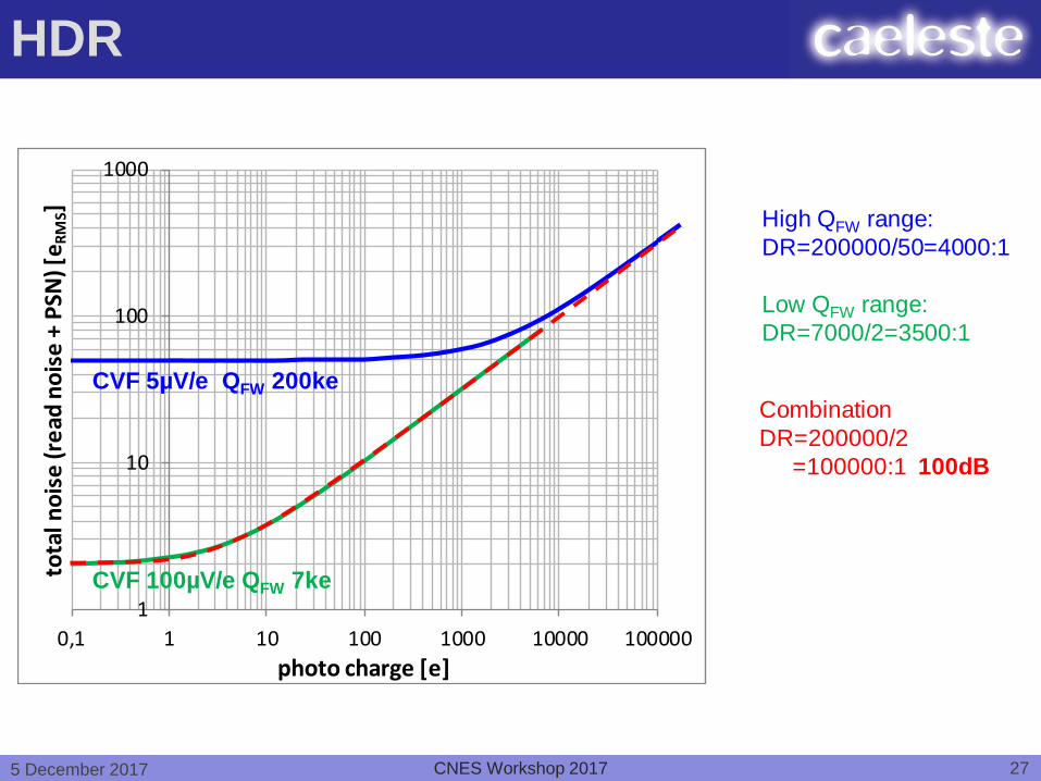
HDR
CNES Workshop 2017
High QFW range:
DR=200000/50=4000:1
Low QFW range:
DR=7000/2=3500:1
1
10
100
1000
0,1 1 10 100 1000 10000 100000
tota
l no
ise
(re
ad n
ois
e +
PSN
) [e R
MS]
photo charge [e]
CVF 5µV/e QFW 200ke
CVF 100µV/e QFW 7ke
Combination
DR=200000/2
=100000:1 100dB