eu centre of excellence in pv materials and devices pv-est fw project enk6-ct-2002-80664 enn...
TRANSCRIPT

EU Centre of Excellence in PV Materials and Devices
PV-EST
FW project ENK6-CT-2002-80664
Enn Mellikov

Motivation of project
Project defined its objectives as follows: • capacity building of the laboratory via
increasing its international attraction • strengthening of position of laboratory as
the leading centre of fundamental and applied research in PV materials
• realization of technology development potential of Tallinn team.

Tools to reach goals of projects
• Exchange of scientists
• R/D activities in laboratory
• Creating of up-to-date infrastructure for R/D activities

WHO WE ARE !WHO WE ARE !
2002 - European Union Centre of Excellence in PV Materials and Devices
2002 - National Centre of Excellence in Materials Science and Chemistry2007 – Partner in virtual Nordic Centre of Excellence in PV Three times Estonian Scientific Award in Sciences for
Research in the Field of Development of New PV Materials and Solar Cells (1985, 1998, 2005)
Research staff 39Junior researchers 18PhD students 15PhD defended 2004-2006 7

WHO WE AREWHO WE ARE,, research staff, intellectual capacity

WHO WE AREWHO WE ARE,, exchange of scientists, 2003-2007
• Outward visits 25
• Inward visits 16
• International Summer School in PV Materials and Devices
2006, 52 participants, 11 countries

WHO WE AREWHO WE ARE, equipment, equipment
90% of scientific and technological equipment newer than 5 years
Unique equipmenthigh resolution scanning electron microscope Zeiss Ultra 55 with EDS, WDX and EBIC systems,
Raman spectrometer HORIBA JOBIN YVON S.A.S. electron gun evaporation system, Vacuumservice (Finland)magnetron sputtering system, AJA (USA)plasma treatment system, (Germany)impedance spectrometers, (USA, Germany)..............

WHO WE AREWHO WE ARE, LABORATORY, LABORATORY

WHO WE AREWHO WE ARE, equipment, equipment
Unique equipment, planned investments during years 2007-2008 1.6 million EURO
Inert gas cabinet with built-in vacuum evaporator planned 2007
XPS planned 2007XRD system for thin film planned 2007Profilometer planned 2007-2008ICP-MS with laser ablation system planned 2007-2008SEM sample preparation system planned 2007

WHO WE AREWHO WE ARE, EUROPE, EUROPE ! !
• 2003 - 2006 FW project The European Polymer Solar Battery (ENK5-CT-2002-00687) – EURO-PSB • 2003 - 2006 FW project Materials and Technologies for Photovoltaic Applications from Estonia (ENK6-CT-2002-80664 ) – PV-EST • 2002 - 2006 FW project Co-ordination of NAS and European Union RTD Programmes on Photovoltaic Solar Energy (NNE5-2002-00046) • 2004-2007 FW project 502775 (SES6) European Collaboration for identification of PV research and market opportunities, socio-economic studies, performance assessment and dissemination of PV thermal technology “PV-Catapult” • 2004-2007 INTAS project Science and Technology of Copper-indium Chalcogenites and Organic Conductive Polymers Based PV Solar Cells •2004-2006 INTAS project Optical and structural analysis of single crystals and thin films of CuIn3Se5, CuGa3Se5, CuIn4Se6, CuIn5Se8,
CuGa5Se8 for photovoltaic applications •2007-2009 FW 6 project “Performance”
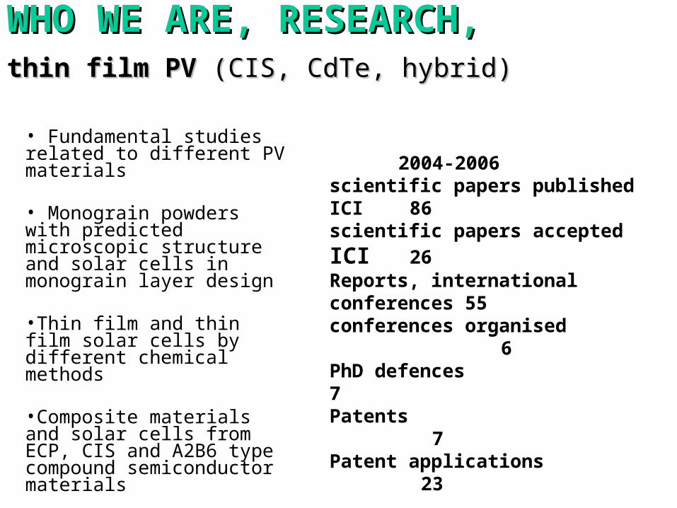
WHO WE AREWHO WE ARE, RESEARCH,, RESEARCH, thin film PV thin film PV (CIS, CdTe, hybrid)(CIS, CdTe, hybrid)
• Fundamental studies related to different PV materials
• Monograin powders with predicted microscopic structure and solar cells in monograin layer design
•Thin film and thin film solar cells by different chemical methods
•Composite materials and solar cells from ECP, CIS and A2B6 type compound semiconductor materials
2004-2006scientific papers published ICI 86
scientific papers accepted ICI 26Reports, international conferences 55conferences organised 6PhD defences 7Patents 7Patent applications 23

Photoluminescence studies
PL spectra of stoichiometric CuInTe2 at 11K
PL spectrum of stoichiometric CuInSe2 at 11K
0,92 0,94 0,96 0,98 1,00 1,02
A
B
T=10K
E (eV)
Measured Fitted
PL
inte
nsity
(a.
u.)
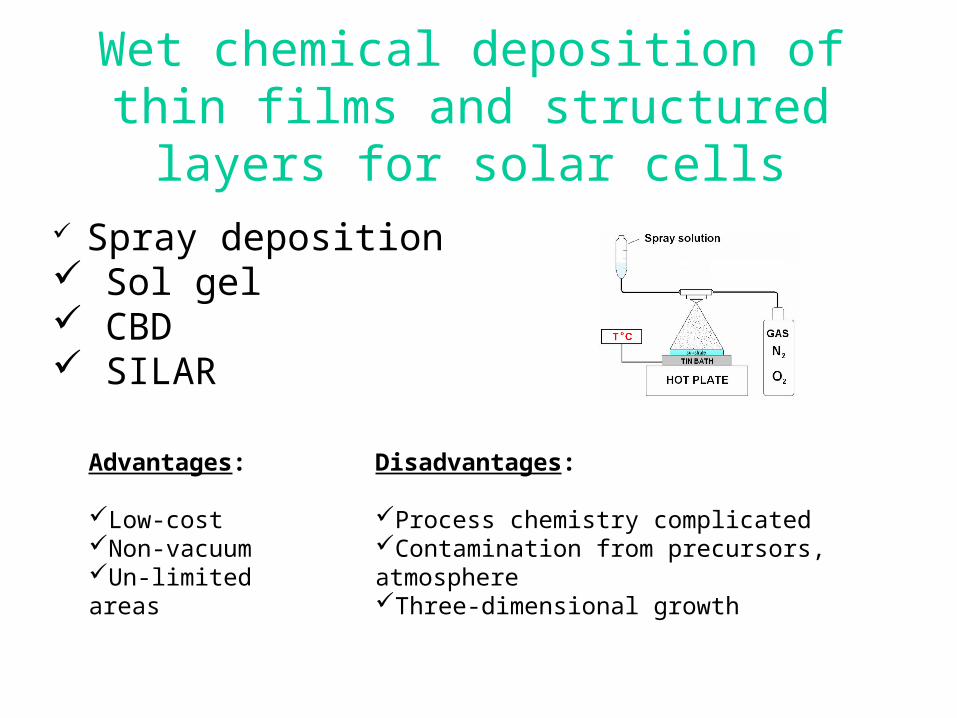
Wet chemical deposition of thin films and structured layers for solar cells
Spray deposition Sol gel CBD SILAR
Advantages:
Low-costNon-vacuumUn-limited areas
Disadvantages:
Process chemistry complicated Contamination from precursors, atmosphereThree-dimensional growth

Solar cell by spray technique
1 m
Päikesekiirgus
Klaas
CuInS2
CdSZnOITO
-0.4 -0.2 0.0 0.2 0.4 0.6
-20
-10
0
10
20
j, m
A/c
m2
Pinge, V
TiO2/In(OH)
xS
y/CIS
ZnO/CdS/CIS1+CIS2 ZnO/CdS/CIS
Solar cell structures prepared by on-line deposition in air:Efficiencies : ~3 %Preparation time: < 1hCost : very low

Monograin powder of CuInSe2
The advantages of the developed powder materials are:
1. single-crystalline structure of every grain;
2. narrow granulometric
composition;
3. uniform molecularity, stoichiometry and distribution of doping impurities in material

Monograin layer

Advantages of MGL
MGL combines high photoelectric parameters of monocrystals and advantages of polycrystalline materials and technologies:
1) low cost and simple technology of materials and devices;
2) possibility of making devices of a practically unlimited area;
3) possibility of using materials 100%

Schematic drawing and photograph of Cu/CIS/PEDOT-PSS/Cr/Au structure
Copper tape ~ 0.1 mm
Cu-In alloy ~ 300 nm
Top contact-window layer: Cr (1-2nm)/Au (20nm)+ Au strip (thickness 200 nm, width 2 mm)
PEDOT-PSS (50 nm) or ZnPc (20 nm) buffer layer
i-CIS ~ 200 nm
In-rich n-CIS ~ 1300 nm
p
i
n

PV panels testing Center
• The first test facility (32 m2) of PV panels in the Baltic states is installed on the roof of one building of TTU, EU FW6 project “Performance”.
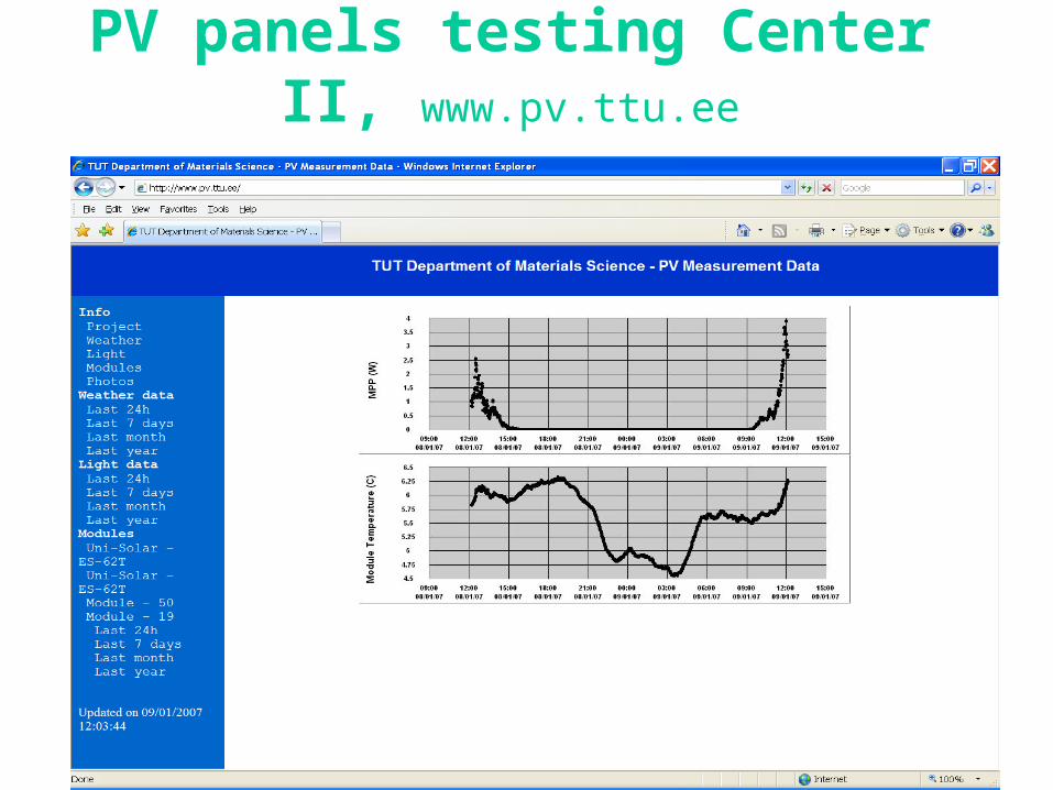
PV panels testing Center II, www.pv.ttu.ee

We have a dream: Estonia in the future

Thank you for attention