et zc344-l5 part2
DESCRIPTION
Instrumentation and Process Control Lecture 5 Part 2TRANSCRIPT
BITS PilaniPilani Campus
Instrumentation and controlET ZC 341
1
Swapna KulkarniLecturer

BITS PilaniPilani Campus
Operational Amplifiers
2

BITS Pilani, Deemed to be University under Section 3 of UGC Act, 1956
Voltage Follower Figure : The Op amp voltage follower. This circuit
has unity gain but very high input impedance • Figure shows an opamp circuit with unity gain and very high input impedance. The input impedance is essentially the input impedance of the op amp itself, which can be greater than 100M . The voltage output tracks the input over a range defined by the plus and minus saturation voltage outputs.
3
Copyright ©2006 by Pearson Education, Inc.Upper Saddle River, New Jersey 07458
All rights reserved.

BITS Pilani, Deemed to be University under Section 3 of UGC Act, 1956
• Current output is limited to the short circuit ofop amp, and output impedance is typicallymuch less than 100 . In many cases, amanufacturer will market an opamp voltage
follower whose feedback is provided internally.
4

BITS Pilani, Deemed to be University under Section 3 of UGC Act, 1956
• Such a unit is usually specifically designed forvery high input impedance. The unity gainvoltage follower is essentially an impedancetransformer in the sense of converting avoltage at high impedance to the samevoltage at low impedance.
5

BITS Pilani, Deemed to be University under Section 3 of UGC Act, 1956
This connection forces the op-amp to adjust its output voltage simply equal to the input voltage (Vout follows Vin so the circuit is named op-amp voltage follower). The importance of this circuit does not come from any change in voltage, but from the input and output impedances of the op-amp.

BITS Pilani, Deemed to be University under Section 3 of UGC Act, 1956
Inverting Amplifier
• Equation shows that this circuit inverts theinput signal and may have either attenuationor gain, depending on the ratio of inputresistance, R1 and feedback resistance R2.
7
inout VR
RV
1
2

BITS Pilani, Deemed to be University under Section 3 of UGC Act, 1956
• It is important to note that the input impedance ofthis circuit is essentially equal to R1, the inputresistance. In general, this resistance is not large, andhence the input impedance is not large. The outputimpedance is low.
8
Copyright ©2006 by Pearson Education, Inc.Upper Saddle River, New Jersey 07458
All rights reserved.

BITS Pilani, Deemed to be University under Section 3 of UGC Act, 1956
9
Figure: The Op Amp summing Amplifier
Copyright ©2006 by Pearson Education, Inc.Upper Saddle River, New Jersey 07458
All rights reserved.
Summing Amplifier

BITS Pilani, Deemed to be University under Section 3 of UGC Act, 1956
Summing Amplifier
• A common modification of the invertingamplifier is an amplifier that sums or adds twoor more applied voltages.
• This circuit is shown in figure for the case ofsumming two input voltages. The transferfunction of this amplifier is given by
10

BITS Pilani, Deemed to be University under Section 3 of UGC Act, 1956
2
3
21
1
2 VR
RV
R
RVout
11
The sum can be scaled by proper selection ofresistors. For example, if we make R1 = R2=R3,then the output is simply the (inverted) sumof V1 and V2. The average can be found bymaking R1 = R3 and R2 = R1/2.

BITS Pilani, Deemed to be University under Section 3 of UGC Act, 1956
Develop an op amp circuit that can provide an output voltage related to the input voltage by Vout=3.4 Vin+5
• Solution: One way is to use a summing amplifier with Vin on
one input and 5 V on the other. The gains will be selected to be 3.4 and 1.0,respectively. The summing amplifier is also an inverter, however, so the sign will be wrong.
Thus, a second amplifier will be used with a gain of -1 to make the sign correct. The result is shown in next slide. Selection of the values of resistors is based on the general notion of keeping the currents in mA.
12

BITS Pilani, Deemed to be University under Section 3 of UGC Act, 1956
13
Figure : The op amp circuit for example.
Copyright ©2006 by Pearson Education, Inc.Upper Saddle River, New Jersey 07458
All rights reserved.

BITS Pilani, Deemed to be University under Section 3 of UGC Act, 1956
Noninverting Amplifier
• A noninverting amplifier may be constructed from an op amp, as shown in figure.
• The gain of this circuit is found by summing the currents at the summing point, S, and using the fact that the summing point voltage is Vin so that no voltage difference appears across the input terminals.
14

BITS Pilani, Deemed to be University under Section 3 of UGC Act, 1956
15
Figure A noninverting amplifier
I1 + I2 = 0 Where I1 = Current through R1
I2 = Current through R2
Copyright ©2006 by Pearson Education, Inc.Upper Saddle River, New Jersey 07458
All rights reserved.

BITS Pilani, Deemed to be University under Section 3 of UGC Act, 1956
• But these currents can be found from Ohm’slaw such that this equation becomes
021
R
VV
R
V outinin
16
Solving this equation for Vout we find
inout VR
RV
1
21
BITS Pilani, Deemed to be University under Section 3 of UGC Act, 1956
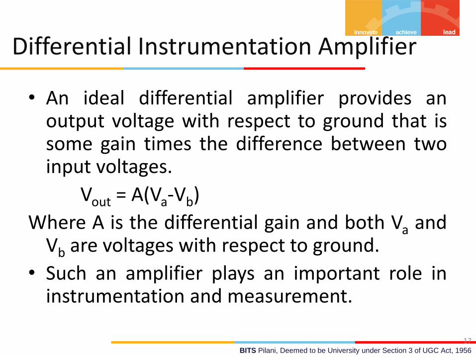
Differential Instrumentation Amplifier
• An ideal differential amplifier provides anoutput voltage with respect to ground that issome gain times the difference between twoinput voltages.
Vout = A(Va-Vb)
Where A is the differential gain and both Va andVb are voltages with respect to ground.
• Such an amplifier plays an important role ininstrumentation and measurement.
17

BITS Pilani, Deemed to be University under Section 3 of UGC Act, 1956
• To define the degree to which a differentialamplifier approaches the ideal, we use thefollowing definition.
18
• The common-mode input voltage is theaverage applied to the two input terminals,
2
bacm
VVV

BITS Pilani, Deemed to be University under Section 3 of UGC Act, 1956
• An ideal differential amplifier will not have anyoutput that depends on the value of thecommon-mode voltage; that is the circuit gainfor common–mode voltage, Acm will be zero.
• The common-mode rejection ration (CMRR) ofa differential amplifier is defined as the ratioof the differential gain to the common-modegain.
19

BITS Pilani, Deemed to be University under Section 3 of UGC Act, 1956
• The common – mode rejection (CMR) is the CMRR expressed in dB.
)(log20 10 CMRRCMR
A
ACMRR
cm
20

BITS Pilani, Deemed to be University under Section 3 of UGC Act, 1956
21
Figure : The basic differential amplifier configuration
Copyright ©2006 by Pearson Education, Inc.Upper Saddle River, New Jersey 07458
All rights reserved.
Differential Amplifier

BITS Pilani, Deemed to be University under Section 3 of UGC Act, 1956
Differential Amplifier
• There are a number of op amp circuit fordifferential amplifiers.
• Notice that the circuit uses two pairs ofmatched resistors, R1 and R2. When thematching is perfect and the op amp is ideal, thetransfer function for this amplifier is given by
22
12
1
2 VVR
RVout

BITS Pilani, Deemed to be University under Section 3 of UGC Act, 1956
• If the resistors are not well matched, the CMR willbe poor. The circuit of figure has a disadvantage inthat its input impedance is not very high and,further is not the same for the two inputs. For thisreason, voltage followers are often used on theinput to provide high input impedance. The result iscalled an instrumentation amplifier.
23
BITS Pilani, Deemed to be University under Section 3 of UGC Act, 1956
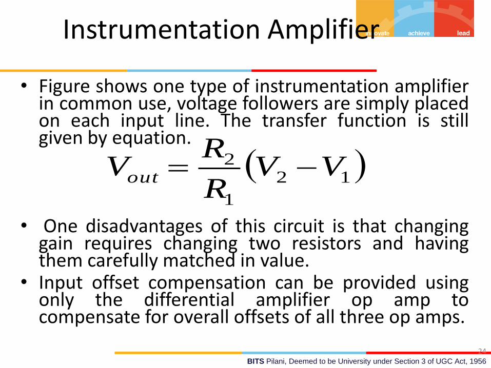
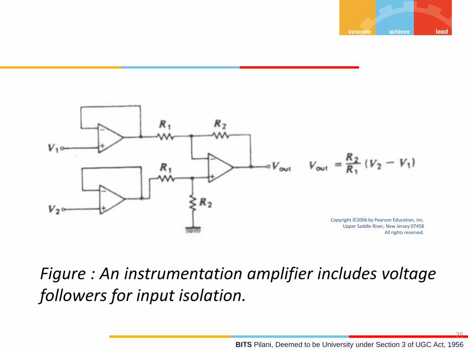
Instrumentation Amplifier
• Figure shows one type of instrumentation amplifierin common use, voltage followers are simply placedon each input line. The transfer function is stillgiven by equation.
• One disadvantages of this circuit is that changinggain requires changing two resistors and havingthem carefully matched in value.
• Input offset compensation can be provided usingonly the differential amplifier op amp tocompensate for overall offsets of all three op amps.
24
12
1
2 VVR
RVout
BITS Pilani, Deemed to be University under Section 3 of UGC Act, 1956
25
Figure : An instrumentation amplifier includes voltagefollowers for input isolation.
Copyright ©2006 by Pearson Education, Inc.Upper Saddle River, New Jersey 07458
All rights reserved.

BITS Pilani, Deemed to be University under Section 3 of UGC Act, 1956
• A more common configuration of instrumentationamplifier, however, is the circuit shown in figure. Thiscircuit allows for selection of gain, within certainlimits, by adjustment of a single resistor, RG. It can beshown that the CMR of this circuit, although stilldependent on careful matching of the differentialamplifier resistors, does not depend on matching ofthe two R1s. The transfer function of this amplifier isgiven by
26
12
2
3121 VV
R
R
R
RV
G
out

BITS Pilani, Deemed to be University under Section 3 of UGC Act, 1956
27
Figure: This instrumentation amplifier allows the gain to be changed using a single resistor
Copyright ©2006 by Pearson Education, Inc.Upper Saddle River, New Jersey 07458
All rights reserved.

BITS Pilani, Deemed to be University under Section 3 of UGC Act, 1956
• The input impedance is very high, and theoutput impedance very low. Many ICmanufacturers provide this circuit with fixeddifferential gain and R1 but allow the user toinsert external RG so the desired gain can beselected. They can thus ensure a high CMR.
28

BITS Pilani, Deemed to be University under Section 3 of UGC Act, 1956
Voltage-to-Current Converter
• Because signals in process-control are mostoften transmitted as a current, specifically 4 to20 mA, it is often necessary to employ a linearvoltage-to-current converter.
• Such a circuit must be capable of sinking acurrent into a number of different loadswithout changing the voltage-to-currenttransfer characteristics.
29

BITS Pilani, Deemed to be University under Section 3 of UGC Act, 1956
30
Figure : A voltage-to-current using an op amp
Copyright ©2006 by Pearson Education, Inc.Upper Saddle River, New Jersey 07458
All rights reserved.

BITS Pilani, Deemed to be University under Section 3 of UGC Act, 1956
• An op amp circuit that provides this function isshown in figure. An analysis of this circuitshows that the relationship between currentand voltage is given by
inVRR
RI
31
2
31

BITS Pilani, Deemed to be University under Section 3 of UGC Act, 1956
• Provided that the resistance are selected sothat
R1(R3+R5)=R2R4
• The circuit can deliver current in eitherdirection, as required by a particularapplication.
32

BITS Pilani, Deemed to be University under Section 3 of UGC Act, 1956
• The maximum load resistance and maximum currentare related and determined by the condition that theamplifier output saturates in voltage. Analysis of thecircuit shows that when the op amp output voltagesaturates, the maximum load resistance andmaximum current are related by
33
543
354
RRR
RI
VRR
Rm
sat
ml

BITS Pilani, Deemed to be University under Section 3 of UGC Act, 1956
34
WhereRml = maximum load resistanceVsat= op amp saturation on voltage Im = maximum current
•A study of equation shows that the maximum load resistance is always less than Vsat/Im. The minimum load resistance is zero.

BITS Pilani, Deemed to be University under Section 3 of UGC Act, 1956
35
Figure : A current-to-voltage converter using an op amp. Care must be taken that the current output capability of the op amp is not exceeded.
Current-to-Voltage Converter
Copyright ©2006 by Pearson Education, Inc.Upper Saddle River, New Jersey 07458
All rights reserved.
BITS Pilani, Deemed to be University under Section 3 of UGC Act, 1956
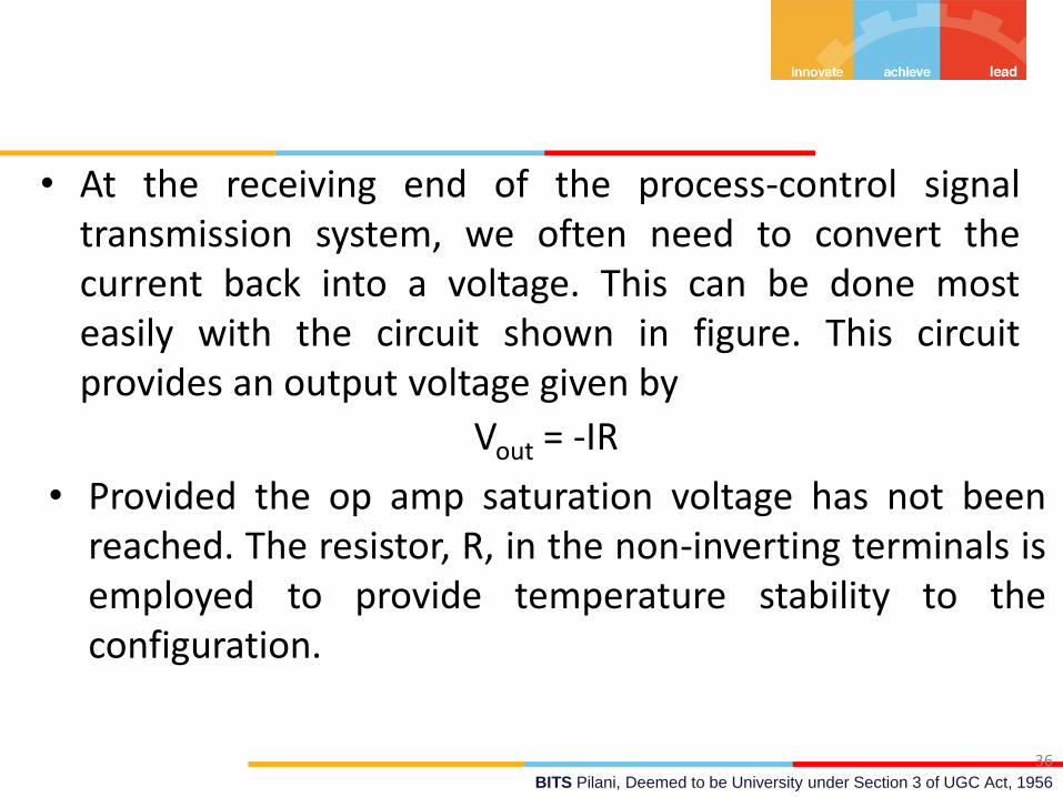
• At the receiving end of the process-control signaltransmission system, we often need to convert thecurrent back into a voltage. This can be done mosteasily with the circuit shown in figure. This circuitprovides an output voltage given by
36
Vout = -IR
• Provided the op amp saturation voltage has not beenreached. The resistor, R, in the non-inverting terminals isemployed to provide temperature stability to theconfiguration.

BITS Pilani, Deemed to be University under Section 3 of UGC Act, 1956
Integrator
Figure An integrator circuit using anop amp.
• Another op amp circuit to be considered is the integrator.
• Integrator is also called as Active low pass filter.
• Using the ideal analysis, we can sum the currents at the summing point as
37
0dt
dVC
R
V outin
Copyright ©2006 by Pearson Education, Inc.Upper Saddle River, New Jersey 07458
All rights reserved.

BITS Pilani, Pilani Campus
• Rearranging the equation and integrating from0 to t, we get
BITS Pilani, Deemed to be University under Section 3 of UGC Act, 1956
39
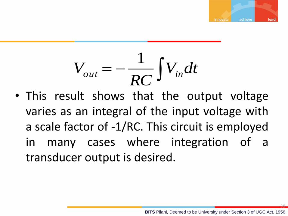
• This result shows that the output voltagevaries as an integral of the input voltage witha scale factor of -1/RC. This circuit is employedin many cases where integration of atransducer output is desired.
dtVRC
V inout
1

BITS Pilani, Deemed to be University under Section 3 of UGC Act, 1956
• Other function also can be implemented, such as ahighly linear ramp voltage. If the input voltage isconstant Vin=K, equation reduces to
tRC
KVout
40
• Which is linear ramp, a negative slope of K/RC. Somemechanism of reset through discharge of thecapacitor must be provided, because otherwise Vout
will rise to the output saturation value and remainfixed there in time.

BITS Pilani, Deemed to be University under Section 3 of UGC Act, 1956
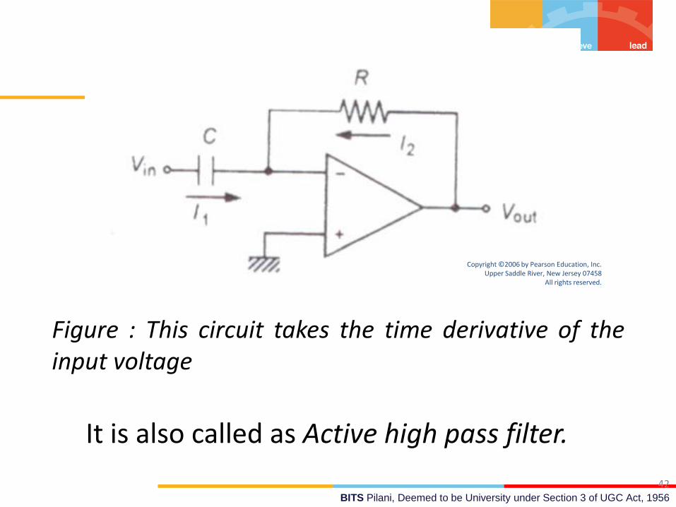
Differentiator
• It is also possible to construct an op ampcircuit with an output proportional to thederivative of the input voltage.
0R
V
dt
dVC outin
41
BITS Pilani, Deemed to be University under Section 3 of UGC Act, 1956
42
Figure : This circuit takes the time derivative of theinput voltage
Copyright ©2006 by Pearson Education, Inc.Upper Saddle River, New Jersey 07458
All rights reserved.
It is also called as Active high pass filter.

BITS Pilani, Deemed to be University under Section 3 of UGC Act, 1956
• Solving for the output voltage shows that the circuit response is
dt
dVRCV in
out
43
Therefore, the output voltage varies as thederivative of the input voltage
Practically speaking, this circuit exhibitserratic or even unstable response and canbe used only in combination with othercircuitry to depress this instability.

BITS Pilani, Deemed to be University under Section 3 of UGC Act, 1956
Linearization
• The op amp can also implement linearization.
• Generally, this is achieved by placing a non-linear element in the feedback loop of the op amp (shown in fig.)
44
F(Vout)
+
VoutRVin
Copyright ©2006 by Pearson Education, Inc.Upper Saddle River, New Jersey 07458
All rights reserved.

BITS Pilani, Deemed to be University under Section 3 of UGC Act, 1956
Linearization
• The summarization of currents provides
Vin/R+I(Vout)=0
where Vin=input voltage
R= input resistance
I(Vout)= nonlinear variation of current with voltage
Eq. is solved (in principle) for Vout, we get
Vout=G(Vin/R)
where Vout=output voltage
G(Vin/R)= a nonlinear function of the input voltage[actually the inverse function of I(Vout)]
45
BITS Pilani, Deemed to be University under Section 3 of UGC Act, 1956
Summary
• To present a complete picture of analog signalconditioning, the following points wereconsidered:
1. The need for analog signal conditioning wasreviewed and resolved into the requirementsof signal-level changes, linearization, signalconversions, and filtering and impedancematching.
46

BITS Pilani, Deemed to be University under Section 3 of UGC Act, 1956
2.Bridge circuits are a common example of aconversion process where a changingresistance is measured either by a current orby a voltage signal. Many modifications of thebridge are used, including electronic balancingand techniques of lead compensation.
3. The high and low pass RC filters are passivecircuits used to block undesired free quenciesfrom data signals.
47

BITS Pilani, Deemed to be University under Section 3 of UGC Act, 1956
• Operational amplifiers (op amp) are a specialsignal-conditioning building block aroundwhich many special – function circuits can bedeveloped. The device was demonstrated inapplications involving amplifiers, converters,linearization circuits, integrators, and severalother functions.
48

BITS Pilani, Deemed to be University under Section 3 of UGC Act, 1956
Digital signal conditioningIntroductionDigital information PLCs Computer interfacing ComparatorsDigital to analog converters Data acquisition systems
Next Class