epson quartz crystal catalog
TRANSCRIPT

TQ 012-30
Product Catalog

CRYSTAL UNIT SPECIFICATIONS 1 2-CRYSTAL OSCILLATOR SPECIFICATIONS 3 5-REAL TIME CLOCK MODULE SPECIFICATIONS 6PACKAGING SPECIFICATIONS 7
-HANDLING PRECAUTIONS 8 10PRECAUTIONS IN DESIGNINGOSCILLATION CIRCUITS 10 11-OUTPUT WAVEFORM AND TEST CIRCUIT 11 12-
Low and medium-frequency
C-4-TYPE 14 (small cylinder)
MC-306 16 (small SMD)MC-206 15 (small SMD)
MC-405/406 17 (SMD)
CA-301 18 (cylinder)CA-303HS 19 (cylinder, high-stability)SA-315H/315HZ 20 (thin cylinder, high-stability)MA-306 21 (small SMD)MA-406 22 (SMD)MA-406H 23 (SMD, high-stability)
Serial interface
Parallel interface
MA-505/506 24 (SMD)FA-365/367/368 25 (thin SMD)
REFERENCE DATA (SG-51/531/615/636 series) 31
SG-10 26 (SIP)
SG-11 27 (SIP)
(SMD)HG-1000/2000 series 36High-stability
MG-7010 39 (selectable output)Multi-output
RTC-4513 43 44- (32 KHz output)RTC-4543 45 46-
SG-51/SG-531 series (through hole) 28
(programmable output)MG-3020 40 (selectable output)SPG series 41 42-
SG-615 series (SMD) 29SG-636 series (small SMD) 30
SG-8002DB/DC series 32 (DIP)SG-8002JA series (SMD) 33SG-8002JC series (small SMD) 34SG-8002CA series (thin SMD) 35
VG-1011JA series (SMD) 37VG-2320SC series (SMD) 38
(high-frequency stability)RTC-4553 47 48-
RTC-58321/58323 (4-bit) 51 52-RTC-62421/62423 (4-bit) 53 54-
(4-bit)RTC-72421/72423 55 56- (4-bit)RTC-63421/63421M/63423 57 58-
RTC-64611/64613 (8-bit) 59 60- (8-bit)RTC-65271 61 62-
RTC-6593 (8-bit for PC/AT) 63 64-
GLOSSARY 67
(SAW resonator) 66FS-555
CONTENTS
49 50-RTC-8583/8593 (I C-Bus interface compatible)2
C-2-TYPE/C-TYPE 13 (cylinder)
High-frequency
Low and medium-frequency
High-frequency
HTS-206 65(cylinder)
APPLICATIONS GUIDE
CRYSTAL UNIT DATA SHEETS
CRYSTAL OSCILLATOR DATA SHEETS
REAL TIME CLOCK MODULE DATA SHEETS
Voltage-controlled crystal oscillator
TEMPERATURE SENSOR DATA SHEETS
SURFACE ACOUSTIC WAVE DEVICE DATA SHEETS

1
Applications guide
Frequency range
Specifications
Frequency and temperature characteristics example
TABLE OF CRYSTAL UNITS32.768 KHz
20 KHz 100 KHz 1 MHz 24 MHz 40 MHz 64 MHz
20 KHz to 165 KHz, 307.2 KHz32 KHz to 120 KHz, 192 KHz
20 KHz to 165 KHz20 KHz to 165 KHz, 307.2 KHz
4 MHz to 64 MHz17.7 MHz to 41 MHz
4 MHz to 64 MHz
9.6 MHz to 27 MHz
10 MHz to 27 MHz
32.768 KHz32.768 KHz32.768 KHz
32 KHz to 100 KHz
14 MHz to 41 MHz
∗1
∗1∗1
∗2
∗2
0
-10
-20
-30
-40
-50
-60
-70
-20 -10 0 10 20 30 40 50 60 70 -40
-60
-40
-20
0
20
40
-20 0 20 40 60 80 100
Freq
uenc
y
f/
f (pp
m)
Temperature (˚C)
Tuning fork crystal units
Temperature (˚C)
AT-cut crystal units
Typical T=25˚Ca=-0.035ppm/˚C 2
Freq
uenc
y
f/
f (pp
m)
θ
Low and medium-frequency
crystal units
(tuning fork crystal units)
High-frequency
crystal units
(AT-cut crystal units)
ModelC-001R
C-002RXC-004RC-005R
C-2-TYPEC-4-TYPEMC-206MC-306
MC-405/406CA-301MA-306MA-406
MA-505/506CA-303HSMA-406H
SA-315H/HZFA-365/7/8
ø3.1 x 8.0ø2.0 x 6.0ø1.5 x 5.0ø1.2 x 4.6
ø2.0 x 6.0
ø1.5 x 5.0
7.3 x 4.1 x 2.08.0 x 3.8 x 2.54
10.4 x 4.1 x 3.56
ø3.1 x 8.9ø3.1 x 10.3
8.0 x 3.8 x 2.54
11.7 x 4.8 x 3.7
13.5 x 5.1 x 4.57
ø3.1 x 8.9
11.7 x 4.8x 3.7
8.0 x 3.0x 1.55
6.2 x 3.7x 1.4
32.768 KHz ±20ppm
L x W x H (mm)
Item Dimensions Nominal frequency Frequency tolerance(standard)
Frequency temperature characteristics Series resistance Load capacitance Storage temperature
rangeOperating
temperature rangef ∆f/f R1 CL TSTG TOPR
20KHz to 165KHz307.2 KHz
32 KHz to 120 KHz192 KHz
32 KHz to 100 KHz
20 KHz to 165 KHz20 KHz to 165 KHz
307.2 KHz
4 MHz to 64 MHz
4 MHz to 64 MHz
9.6 MHz to 27 MHz
14 MHz to 41 MHz
17.734 MHz to 41 MHz
Peak temperature (θT):25˚C typ.
Temperature coefficient
(a): -0.035ppm/˚C2 typ.∆f/f (ppm) =a (θ T -θ X)2
35 KΩ to 50 KΩ
±20 to ±100ppm
±3 to ±20ppm
±30ppm
±30ppm
±30ppm
±50ppm
±50ppm,±100ppm
±10ppm
±20 to ±100ppm
±50 to ±100ppm
±30ppm (±50ppm)
±30ppm (±50ppm)
10 to 55 KΩ
6 to 55 KΩ
6 to 55 KΩ
40 to 150 Ω
40 to 150 Ω
25 to 50 Ω
30 to 40 Ω
50 Ω
60 KΩ
6pF to ∞
10pF to ∞
Fundamental: 10pF to ∞,3rd overtone: 5pF to ∞
-20 to +70˚C -10 to +60˚C
-40 to +85˚C
-20 to +70˚C
-40 to +85˚C
-20 to +70˚C
-55 to +125˚C
-40 to +85˚C
-55 to +100˚C
-55 to +125˚C
∗ 1 Since there are unavailable frequencies, please be sure to contact your nearest distributor or please refer to the frequency list. (page 14)∗ 2 8.0 MHz < f < 8.2 MHz: unavailable. For frequencies less than 5.5MHz, please refer to the frequency list. (page 18)
Note: For detailed specifications, refer to the individual specifications for each product.
C-001RC-002RXC-004RC-005R
C-2-TYPE
C-4-TYPEMC-206
MC-306
MC-405/406
CA-301
MA-306
MA-406
MA-505/506
CA-303HS
MA-406H
SA-315H/HZ
FA-365/7/8
10 MHz to 27 MHz
15 to 55 KΩ

2
Applications guide
Dimensions (Unit: mm)
Cylinder SA-315H
SA-315HZ
SMD
D1
L1 L2
B
D2
W3
B
H1 H2W
1
W2
L1
H
L
W
L3 L3 W2 W2
B
H1 H2H3
W1
L2
L1
W3
B
H1 H2W
1
W2
L1
(L3) (L3)L2
D2
D2
1.1
L1 L2
L3
W2
W1
W1
D1D1
L1 L2
1.1
ModelC-001R
C-002RX/C-2-TYPEC-004R/C-4-TYPE
C-005R
Over 5.5 MHzUnder 5.5 MHz
CA-301
CA-303HS
L1
8.0 max.
6.0 max.
5.0 max.
4.6 max.
8.9 max.
10.3 max.
8.9 max.
L2
9.0 min.
4.0 min.
4.0 min.
4.0 min.
9.5 min.
9.5 min.
9.5 min.
D1
ø3.1 max.
ø2.0 max.
ø1.5 max.
ø1.2 max.
ø3.1 max.
ø3.1 max.
ø3.1 max.
D2
ø0.3
ø0.2
ø0.2
ø0.15
ø0.3
ø0.3
ø0.3
B
1.1
0.7
0.5
0.3
1.1
1.1
1.1
ModelSA-315HSA-315HZ
L1
8.0 max.8.0 max.
L2
7.5 min.2.0 min.
L3
–0.7 min.
W1
3.0 max.3.0 max.
W2
–2.5 max.
D1
1.551.55
D2
ø 0.3ø 0.3
B1.11.1
Model
MC-206
L1
7.3 max.
W1
4.1
W2
2.5W3
0.4
H1
1.8
H2
2.0 max.
B
5.08
Model
MC/MA-306
MA-406/406H
L1
8.0 max.
11.7 max.
L2
1.9
2.1
L3
(0.9)
(1.2)
W1
3.8 max.
4.8 max.
W2
3.2
4.0
W3
0.5
0.7
B
5.5
9.6
H1
2.38
3.50
H2
2.54 max.
3.7 max.
Model
MC-405/406
MA-505/506
Model
FA-365/367/368
L1
9.6
12.7
L2
10.41 max.
13.46 max.
L
6.2 max.
W
3.7 max.
H
1.4 max.
L3
2.54
2.54
W1
4.06 max.
5.08 max.
W2
0.51
1.09
B
2.29
3.30
H1
3.15
4.19
H2
3.60 max.
4.60 max.
H3
0.2 min.
0.2 min.

3
Applications guide
Frequency range
Specifications
TABLE OF CRYSTAL OSCILLATORS0.005 Hz to 1 MHz
0.00027 Hz to 153.6 KHz0.00027 Hz to 100 KHz
10 Hz to 153.6 KHz1.5 MHz to 24 MHz
1.025 MHz to 26.00 MHz
2.2 MHz to 41 MHz
41 MHz to 70 MHz
2.2 MHz to 40 MHz
1.5 MHz to 28.6363 MHz
1.1 MHz to 40 MHz20 MHz to 120 MHz
26.0001 MHz to 66.6667 MHz
12 MHz to 20 MHz
1 Hz 100 KHz 1 MHz 26 MHz 40 MHz 67 MHz 125 MHz
ItemModel
Low and medium-frequencycrystal oscillators(builtin tuning fork crystal unit)
High-frequency crystaloscillators(builtin AT-cut crystal unit)
High-stability oscillators
Voltage-controlled crystal oscillator data sheets
Multi-output crystal oscillators(builtin AT-cut crystal unit)
ModelSPG-8640 seriesSPG-8650 seriesSPG-8651 seriesSG-10SG-11SG-51PSG-531PSG-615PSG-51PTJSG-531PTJSG-615PTJSG-51PHSG-531PHSG-615PHSG-636PTFSG-636PTJSG-636PHSG-636SCESG-636PCEHG-1012JAHG-2012JAVG-1011JAVG-2320SCMG-3020MG-7010
SPG-8640 series
SPG-8650 series
SPG-8651 series
SG-10
SG-11
SG-51PSG-531PSG-615P
SG-51PTJSG-531PTJSG-615PTJ
SG-51PHSG-531PHSG-615PH
SG-636PTF
SG-636PTJ
SG-636PH
SG-636SCESG-636PCEHG-1012JAHG-2012JA
VG-1011JA
VG-2320SC
MG-3020
MG-7010
Output frequency range
0.005 Hzto 1 MHz
0.00027 Hzto 153.6 KHz
0.00027 Hzto 100 KHz
10 Hz to 153.6 KHz
1.5 MHzto 24 MHz
1.025 MHzto 26.00 MHz
26.0001 MHzto 66.6667 MHz
2.2 MHzto 41 MHz
41 MHzto 70 MHz
2.2 MHzto 40 MHz
1.5 MHzto 28.6363 MHz
12 MHzto 20 MHz
1.1 MHzto 40 MHz
20 MHzto 120 MHz
Frequencystability
±100ppm
±50ppm
±5ppm
±50ppm (±10ppm)
±100ppm
±15 to±30ppm
±15 to±25ppm
±15ppm
±100ppm
Currentconsumption
2mA max.
0.5mA max.
10mA max.
23mA max.
35mA max.
17mA max.
35mA max.
9mA max.
10mA max.
2.5mA max.
20mA max.
27mA max.
Package type
DIP 16-pin
SIP 3-pin
DIP 14-pinDIP 8-pin
SMDDIP 14-pinDIP 8-pin
SMDDIP 14-pinDIP 8-pin
SMD
DIP 14-pin
SOP 14-pin
Operatingtemperature
-10˚C to +70˚C
-10˚C to +60˚C
-10˚C to +70˚C
-20˚C to +70˚C
-40˚C to +85˚C
-20˚C to +75˚C
-10˚C to +70˚C
Operatingvoltage
5V ±0.5V
3.3V ± 0.3V
5V ±0.25V
5V ±0.5V
3V ±0.3V
5V ±0.25V
2.7V to 5.5V
Output load
TTL 1CL 15pF
TTL 10CL 50pF
TTL 5
CL 50pF
TTL 5
CL20pF( < 55 MHz)CL15pF ( > 55 MHz)
CL 30pF
CL 15pF
TTL 2 CL 15pF
2KΩ // 10pF
CL 15pF
Output control
RESET
—
OE
ST
OE
—
RESET
ST/OE
• OE: Output enable• ST: Stand-by (low level)• For detailed specifications, refer to the individual specifications for product.
4
Applications guide
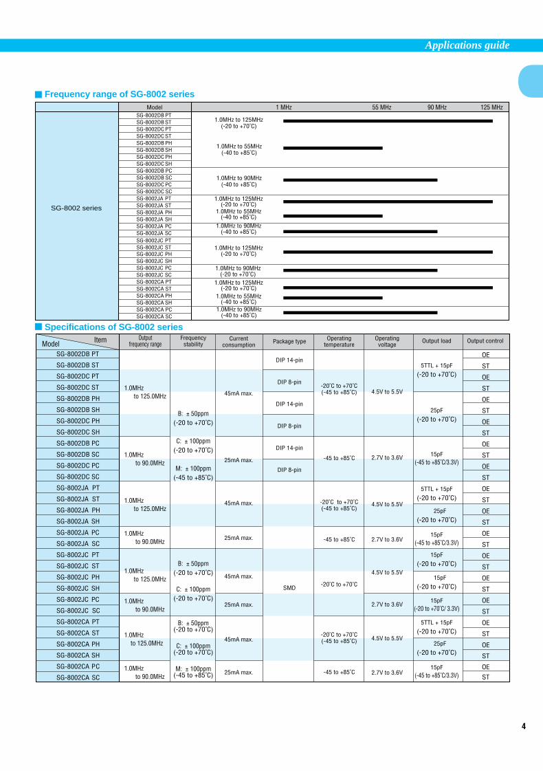
Frequency range of SG-8002 series
Specifications of SG-8002 series
1 MHz 55 MHz 90 MHz 125 MHz
ItemModel
ModelSG-8002DB PTSG-8002DB STSG-8002DC PTSG-8002DC STSG-8002DB PHSG-8002DB SHSG-8002DC PHSG-8002DC SHSG-8002DB PCSG-8002DB SCSG-8002DC PCSG-8002DC SCSG-8002JA PTSG-8002JA STSG-8002JA PHSG-8002JA SHSG-8002JA PCSG-8002JA SCSG-8002JC PTSG-8002JC STSG-8002JC PHSG-8002JC SHSG-8002JC PCSG-8002JC SCSG-8002CA PTSG-8002CA STSG-8002CA PHSG-8002CA SHSG-8002CA PCSG-8002CA SC
SG-8002DB PT
SG-8002DB ST
SG-8002DC PT
SG-8002DC ST
SG-8002DB PH
SG-8002DB SH
SG-8002DC PH
SG-8002DC SH
SG-8002DB PC
SG-8002DB SC
SG-8002DC PC
SG-8002DC SC
SG-8002JA PT
SG-8002JA ST
SG-8002JA PH
SG-8002JA SH
SG-8002JA PC
SG-8002JA SC
SG-8002JC PT
SG-8002JC ST
SG-8002JC PH
SG-8002JC SH
SG-8002JC PC
SG-8002JC SC
SG-8002CA PT
SG-8002CA ST
SG-8002CA PH
SG-8002CA SH
SG-8002CA PC
SG-8002CA SC
OE
ST
OE
ST
OE
ST
OE
ST
OE
ST
OE
ST
OE
ST
OE
ST
OE
ST
OE
ST
OE
ST
OE
ST
OE
ST
OE
ST
OE
ST
1.0MHz to 125MHz(-20 to +70˚C)
1.0MHz to 55MHz(-40 to +85˚C)
1.0MHz to 90MHz(-40 to +85˚C)
SG-8002 series
1.0MHz to 125MHz(-20 to +70˚C)
1.0MHz to 55MHz(-40 to +85˚C)
1.0MHz to 125MHz(-20 to +70˚C)
1.0MHz to 55MHz(-40 to +85˚C)
1.0MHz to 90MHz(-40 to +85˚C)
1.0MHz to 90MHz(-40 to +85˚C)
1.0MHz to 125MHz(-20 to +70˚C)
1.0MHz to 90MHz(-20 to +70˚C)
Output frequency range
1.0MHz to 125.0MHz
1.0MHz to 90.0MHz
1.0MHz to 125.0MHz
1.0MHz to 90.0MHz
1.0MHz to 125.0MHz
1.0MHz to 90.0MHz
1.0MHz to 125.0MHz
1.0MHz to 90.0MHz
Frequencystability
B: ± 50ppm(-20 to +70˚C)
C: ± 100ppm(-20 to +70˚C)
M: ± 100ppm(-45 to +85˚C)
B: ± 50ppm(-20 to +70˚C)
C: ± 100ppm(-20 to +70˚C)
B: ± 50ppm(-20 to +70˚C)
C: ± 100ppm(-20 to +70˚C)
M: ± 100ppm(-45 to +85˚C)
Currentconsumption
45mA max.
25mA max.
45mA max.
25mA max.
45mA max.
25mA max.
45mA max.
25mA max.
Package type
DIP 14-pin
DIP 8-pin
DIP 14-pin
DIP 8-pin
DIP 14-pin
DIP 8-pin
SMD
Operatingtemperature
-20˚C to +70˚C(-45 to +85˚C)
-45 to +85˚C
-20˚C to +70˚C(-45 to +85˚C)
-45 to +85˚C
-20˚C to +70˚C
-20˚C to +70˚C(-45 to +85˚C)
-45 to +85˚C
Operatingvoltage
4.5V to 5.5V
2.7V to 3.6V
4.5V to 5.5V
2.7V to 3.6V
4.5V to 5.5V
2.7V to 3.6V
4.5V to 5.5V
2.7V to 3.6V
Output load
5TTL + 15pF
(-20 to +70˚C)
25pF
(-20 to +70˚C)
15pF(-45 to +85˚C/3.3V)
5TTL + 15pF
(-20 to +70˚C)
25pF
(-20 to +70˚C)
15pF(-45 to +85˚C/3.3V)
15pF
(-20 to +70˚C)
15pF
(-20 to +70˚C)
15pF(-20 to +70˚C/ 3.3V)
5TTL + 15pF
(-20 to +70˚C)
25pF
(-20 to +70˚C)
15pF(-45 to +85˚C/3.3V)
Output control

5
Applications guide
0.25
6.65
4.5
max
.3.
0 m
in.
0.1
min
.
90˚ to105˚
7.6220.5 max.
17.782.540.5
5.3
max
.2.
54 m
in.
0.2
min
.
6.36
15.24
0.2590˚ to105˚
7.62
19.8 max.
0.2
min
.
5.3
max
.2.
54 m
in.
7.62
0.2590˚ to105˚
7.62
13.7 max.
6.6
0.5
0.5
Dimensions (Unit: mm)
0.5 5.08(1.0) (1.0)
3.6
5.0
2.4
2.7
max
.5.
8 m
ax.
10.5 max.
4.6 max.
0.252.1
(7.5
)(1
.3)
8.8
max
.7.
0
2.54 2.54
16.0 max.
5.3
max
.2.
54 m
in.
0.2
min.
6.36
0.2590˚ to105˚
7.62
19.8 max.
15.242.54
8.65
0.25
9.8
max
.4.
7 m
ax.
4.06
0.25
min
.
1.52
5.08 7.3 to 7.90.51
14.0 max.
7.4±
0.2
3.2±
0.1
5.0
3.1
10.1±0.2
0.150.60.05 min.
0˚ to 10˚
DIP 16-pin (SPG series) SIP 3-pin (SG-10/11)
DIP 14-pin (MG-3020)
SMD (SG-615 series, HG-1012JA/2012JA,SG-8002JA series, VG-1011JA series)
SOP (VG-2320SC series)
SOP 14-pin (MG-7010)
Compatible with full-size metal can(SG-51 series, SG-8002DB series)
Compatible with half-size metal can(SG-531 series, SG-8002DC series)
SMD (SG-636 series, SG-8002JC series)
SMD (SG-8002CA series)
13.0 max.
7.62
9.6
max
.
7.6
1.8
0 m
in. 2.0
max
.
0.5
7.0±0.2
5.08
5.0±
0.2
1.4
-0.1
5+
0.1

6
Applications guide
Characteristics
Dimensions
7.4±
0.2
3.2±
0.1
5.0
3.1
10.1±0.2
0.150.6
0.05 min.
SOP 14-pin (RTC-4513/4543SA/4553/8583/8593)
DIP 16-pin (RTC-58321)
SOP 18-pin (RTC-4543SB/RTC-8593SB)
DIP 18-pin (RTC-62421/72421/63421/63421M)
DIP 24-pin (RTC-64611)
DIP 28-pin (RTC-65271)
SOP 24-pin (RTC-58323/62423/72423/63423/ 64613/6593)
0.25
6.65
4.5
max
.3.
0 m
in.
0.1 m
in.
90˚ to105˚
90˚ to105˚
0˚ to 10˚
7.620.520.5 max.
17.78
0.21.0
2.8
max
.12
.2 m
ax.
7.9
16.3 max.
0.05 min.
(Unit: mm)
23.1 max.
2.54 3.3
0.2
min
.
6.8
4.2
max
.
7.62
0.25
32.0 max.
13.6
4.4
3.3
0.8
15.24
0.25
ModelItem
90˚ to105˚
36.8 max.
14.6
9.0
max
.0.
83.
3
15.24
15.24 to 18.02.54
7.8±
0.2
2.0
max
.
5.4
1.8
11.4±0.2
0.150.60.05 min.
0˚ to 10˚
RTC-4513RTC-4543 SARTC-4543 SB
RTC-4553RTC-8583RTC-8593/ SB
RTC-58321RTC-58323RTC-62421RTC-62423RTC-72421RTC-72423RTC-63421RTC-63421MRTC-63423RTC-64611RTC-64613RTC-65271
RTC-6593
Package
DIP 16-pinSOP 24-pinDIP 18-pinSOP 24-pinDIP 18-pinSOP 24-pin
DIP 18-pin
SOP 24-pinDIP 24-pinSOP 24-pinDIP 28-pin
SOP 24-pin
Counter (time counting)
Second to year,day of the week
1/100sec. to year,day of the week
Second to year and day of the week
Sec. to year,day of the week,and 64Hz to 1Hz
Second to year,day of the week
Access time(synchronous signal cycle)
(CLK: 300ns)
(CLK: 2µs)
(SCL: 10µs)
2µs
120ns
Intel bus:120ns
Motorola bus:220ns
85ns
325ns
Data bit Address bit
32.768 KHz,1 Hz
Serial
SOP 14-pinSOP 18-pin
(CLK: 0.75µs)
4
8
4
6
Memory
4bit x 308bit x 240
—
4bit x 17(select)
4bit
4-kBytes
114-Bytes
Alarm
1/100 sec. to month
Second to month and day of the week
Sec. to date, day of the week and 64 HzSec. to hourSec. to hour and Sec. to month(extended alarm)
Time interval of standard pulse
64 Hz, 1 min., 1 hour
1024 Hz, 10 sec.
—
1024 Hz to 1 hour
64 Hz, 1 second, 1 min.,1 hour
1024 Hz, 128 Hz, 64 Hz, 16 Hz, 2 Hz, 1 sec.,1 min.,10 min.
64 Hz, 32 Hz, 16 Hz, 8 Hz, 4 Hz, 2 Hz, 1 Hz
8192 Hz to 2 Hz
Other features
High-frequency stability (±5ppm)
I2C-bus
I/0 Connection
Intel bus
Intel bus(low current consumption)
Intel bus
Motorola bus
"MOTEL bus" systemSame bus interface andbattery backup as S-RAM
Builtin battery holder
Extended alarm
Note: For detail specifications, refer to the individual specifications for each product.
__
—SOP 14-pin
SOP 14-pin
SOP 14/ 18pin
32.768 KHz OUTPUT—

7
Applications guide
PACKING SPECIFICATIONS1. Cylinder
2. SIP
3. DIP
4. SMD
Direction of feed
D
CB
A
φ1.5 4.0
(Unit: mm)
conductive tube
conductive tube
stopper
stopper
1.3
AB
2.0
1.0R
2.0
W
21.0 1.0R
Reel dimensions (Unit: mm)
ModelSG-531 seriesSG-8002DC seriesSG-51 seriesSG-8002DB seriesSPG seriesMG-3020RTC-58321/6242163421/63421M/72421RTC-64611
RTC-65271
Quantity
35 pcs/tube
25 pcs/tube
18 pcs/tube
15 pcs/tube
Model
SA-315HZMC-206MC-306MC-405/406MA-306SG-8002JC seriesSG-8002CA seriesSG-636 series
MA-406/406HMA-505/506SG-8002JA seriesSG-615 seriesVG-1011JA seriesHG-1012JA/2012JAVG-2320SC
SOP14-pin
SOP18-pinSOP24-pinFS-555, FA-365/367/368
Dimension Tape type(L=left direction)A
8.0
12.0
12.012.016.08.0
B
9.25
13.25
9.2511.5
13.257.25
C
16.0
24.0
16.024.024.012.0
D2.6
∗ 1
∗ 2
3.652.862.95∗ 3
TE1608R
TE1608L
TE2412L
TE1612L
TE2416L
TE1208L∗ 1 MC-306,MA-306: 3.0; MC-405/406: 3.9; SG-8002JC/CA; SG-636 series: 3.3; MC-206: 2.2; ∗ 2 MA-406/406H: 4.0; MA-505/6, SG-8002JA, 615 series, HG-1012JA/2012JA: 4.8, VG-1011JA,
VG-2320SC: 2.2 ∗ 3 FS-555: 2.0; FA-365/367/368: 1.6
(2) Tube packingThese are placed into conductive IC tubes per lot of 25 to 55pcs./tube and packed into boxes for shipment.
Note: The above is shown in the standard packing specifications. Small-lot or sample orders may be submitted in a differentpacking style.
Cylinder products are packed in vinyl bags per lot of 250 to 1,000pcs. From 5 to 20 bags are then placed in inner boxes tomake a lot. Inner boxes are then placed in cartons for shipment. (the quantity varies with the model.)
SIP products are packed in inner boxes per lot of 100pcs. They are then placed onto the conductive foam and placed in cartonsfor shipment.
DIP products are placed into conductive IC tubes and packed into boxes for shipment.
(1) Tape and reel packing These are packed for shipment in boxes per lot of 1,000 pcs/reel in accordance with taping standards EIA-481A and EIAJ-1009B.(leader tape: min.1,000mm; trailer tape: min.10 empty pockets)MC/MA-306, MC-206 and SA-315HZ is packed per lot of 3,000pcs. /reel (max.). (3,000 and 1,000)
Model DimensionA
Ø330 Ø80
17.5
25.5
24.4
13.5
13.0Ø60Ø180
17.5Ø80Ø255
B W
MC-206·MC-306·MC-405/406·MA-306·SA-315HZ·SG-8002JC series·SG-636 series·SOP14-pin
SOP18-pin
FS-555
FA-365/367/368
SG-8002CA series
MA-406/406H·MA-505/506SG-8002JA seriesSG-615 seriesHG-1012JA/2012JAVG-1011JASOP24-pinVG-2320SC
8
Applications guide
Common points for all products
HANDLING PRECAUTIONS
1. Shock resistance
2. Heat resistance
3. Soldering heat resistance
4. Ultrasonic cleaning
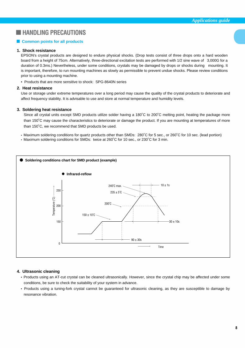
Soldering conditions chart for SMD product (example)
Infrared-reflow
Time
Tem
pera
ture
(˚C)
0
150
200
250
240˚C max.
235 ± 5˚C
150 ± 10˚C
10 ± 1s
30 ± 10s
90 ± 30s
200˚C
EPSON's crystal products are designed to endure physical shocks. (Drop tests consist of three drops onto a hard woodenboard from a height of 75cm. Alternatively, three-directional excitation tests are performed with 1/2 sine wave of 3,000G for aduration of 0.3ms.) Nevertheless, under some conditions, crystals may be damaged by drops or shocks during mounting. Itis important, therefore, to run mounting machines as slowly as permissible to prevent undue shocks. Please review conditionsprior to using a mounting machine.
• Products that are more sensitive to shock: SPG-8640N series
Use or storage under extreme temperatures over a long period may cause the quality of the crystal products to deteriorate andaffect frequency stability. It is advisable to use and store at normal temperature and humidity levels.
Since all crystal units except SMD products utilize solder having a 180˚C to 200˚C melting point, heating the package more
than 150˚C may cause the characteristics to deteriorate or damage the product. If you are mounting at temperatures of more
than 150˚C, we recommend that SMD products be used.
• Maximum soldering conditions for quartz products other than SMDs: 280˚C for 5 sec., or 260˚C for 10 sec. (lead portion)• Maximum soldering conditions for SMDs: twice at 260˚C for 10 sec., or 230˚C for 3 min.
• Products using an AT-cut crystal can be cleaned ultrasonically. However, since the crystal chip may be affected under some
conditions, be sure to check the suitability of your system in advance.
• Products using a tuning-fork crystal cannot be guaranteed for ultrasonic cleaning, as they are susceptible to damage by
resonance vibration.

9
Applications guide
5. Handling of lead terminal
Installation example
6. Handling of reels
7. Storage
1. Drive level
2. Negative resistance
3. Load capacitance
1. Static electricity
Crystal unit
Crystal oscillator and real time clock module
solderPrint circuit board
Direct soldering to the case may impair the characteristics.More than 0.5mm
Pulling the lead strongly may cause cracking of the hermetic glass seal at the root of the lead and lower the airtightness, thusdeteriorating the characteristics. If it is necessary to install the product as in the figure below, leave more than 0.5 mm of leadfrom the case. When the lead needs to be repaired, do not pull on it, and hold the bent part to correct it.
(1) Cylindrical products
When leads are soldered directly to the board pattern, avoid applying stress sufficient to deform the leads. Particular caremust be taken with SOP products.
(2) SMD products
If leads need to be bent, bend the part beyond the stand-off (1.3 mm or more from the case).
(3) SIP products
Deformed leads cannot be inserted into board holes.Avoid applying an stress sufficient to deform leads.
(4) DIP products
(1) Products should be stored at the normal temperature and humidity (refer to the standard conditions of test site JIS Z-8703).Avoid storing them over a long period and mount them immediately after unpacking.
(2) Please carefully handle the inner and outer boxes and reel. External pressure may cause deformation of reel and tape.
We recommend storing products at 15˚C to 35˚C and 25%RH to 85%RH.
Applying excessive drive level to the crystal units may cause deterioration of characteristics or damage. Circuit design must be such as to maintain a proper drive level. (page 10)
Unless adequate negative resistance is allocated in the oscillation circuit, oscillation start up time may increase or oscillationmay not occur at all. To avoid this, provide enough negative resistance in the circuit design. (refer to page 10 "AIIowance for Oscillation".)
Differences in the load capacitance in the oscillation circuit may result in deviations in the oscillation frequency from thedesired frequency. Attempting to tune by force may merely cause abnormal oscillation. Before use, please specify the loadcapacitance of the oscillation circuit. (page 11)
Although an anti-static-electricity protection circuit is provided in the circuit, excessive levels of static electricity may damagethe IC. Choose conductive materials for packing and container. Use a soldering gun and a measuring circuit free from high-voltage leak and provide grounding connection when working with them.
AII crystal oscillators and real time clock modules are provided with a C-MOS IC. Please pay attention to the following points.
10
Applications guide
2. Noise
3. Power supply line
4. Output load
5. Treatment of unused input terminals
6. Heat impact
7. Mounting direction
1. Drive level
2. Allowance for oscillation
How to check the allowance for oscillation
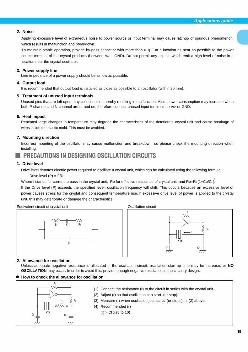
PRECAUTIONS IN DESIGNING OSCILLATION CIRCUITS
R1
RD
Rf
I
X'tal
CDCG
C1L1
C0
RD
Rf
(r)
X'talCDCG
Applying excessive level of extraneous noise to power source or input terminal may cause latchup or spurious phenomenon,
which results in malfunction and breakdown.
To maintain stable operation, provide by-pass capacitor with more than 0.1µF at a location as near as possible to the power
source terminal of the crystal products (between VDD - GND). Do not permit any objects which emit a high level of noise in a
location near the crystal oscillator.
Line impedance of a power supply should be as low as possible.
It is recommended that output load is installed as close as possible to an oscillator (within 20 mm).
Unused pins that are left open may collect noise, thereby resulting in malfunction. AIso, power consumption may increase whenboth P-channel and N-channel are turned on, therefore connect unused input terminals to VDD or GND.
Repeated large changes in temperature may degrade the characteristics of the deteriorate crystal unit and cause breakage of
wires inside the plastic mold. This must be avoided.
Incorrect mounting of the oscillator may cause malfunction and breakdown, so please check the mounting direction wheninstalling.
Drive level denotes electric power required to oscillate a crystal unit, which can be calculated using the following formula.
Drive level (P) = I2Re
Where I stands for current to pass in the crystal unit, Re for effective resistance of crystal unit, and Re=R1 (1+Co/CL) 2
.
If the Drive level (P) exceeds the specified level, oscillation frequency will shift. This occurs because an excessive level of
power causes stress for the crystal and consequent temperature rise. If excessive drive level of power is applied to the crystal
unit, this may deteriorate or damage the characteristics.
Equivalent circuit of crystal unit Oscillation circuit
Unless adequate negative resistance is allocated in the oscillation circuit, oscillation start-up time may be increase, or NOOSCILLATION may occur. In order to avoid this, provide enough negative resistance in the circuitry design.
(1) Connect the resistance (r) to the circuit in series with the crystal unit.
(2) Adjust (r) so that oscillation can start (or stop).
(3) Measure (r) when oscillation just starts (or stops) in (2) above.
(4) Recommended (r)
(r) > CI x (5 to 10)

11
Applications guide
3. Load capacitance
4. Reference for setting parameters of oscillation circuit
1. Timing chart
(1) C-MOS load (2) TTL load
OUTPUT WAVEFORM AND TEST CIRCUIT
RD
Rf
IC
X'talCDCG
Tuning fork crystal unit (example)
Frequency and load capacitance characteristics
AT-cut crystal unit (example)
5 10 15 5 10 15
-50
Load capacitance (pF)
f=32.768 KHz
0
50
100
20
-100
Load capacitance (pF)
(Fundamental)f=20 MHz
0
100
200
tTLH
Duty[%]=tw/ t x 100
tTHL
VOLVOH
tt W
80%VDD
VDD
20%VDD
GND
1/2VDD
tTLH tTHL
VOLVOH
tt W
2.4V
VDD
0.4V
GND
1.4V
Frequencyrange
SymbolRF (MΩ)
20 KHz to 60 KHz 20 50010
60 KHz to 165 KHz 10 300
5.5 MHz to 30 MHz 1 0.5 5 to 15
RD (KΩ) CG (pF) CD (pF)
Differences in the load capacitance of the oscillation circuit may result in a different oscillation frequency from the desired one, as
shown in the figure below. Approximate expression of the load capacitance of the circuit CL CG x CD/ (CG +CD) +CS.
Where CS Stands for stray capacity of the circuit.
IC: equivalent to TC74HCU04P(TC74HCU04P is a product number of Toshiba Corp.)
Freq
uenc
y to
lera
nce
[ f
/f (p
pm)]
Freq
uenc
y to
lera
nce
[ f
/f (p
pm)]
( Fundamental )

12
Applications guide
(1) C-MOS load
(3) Current consumption
3. Test conditions
0.01µFto 0.1µF
0.01µFto 0.1µF
VDD OUT
GND
Measuredobject
VDD
CL
CL
TTL1=4 KΩTTL10=390 Ω
OUT
GND
Measuredobject
For CL value, refer tothe specifications of each model.
TESTPOINT
0.01µFto 0.1µF
VDD
A
OUT
+
-
GND
Measuredobject
TESTPOINT
(2) TTL load
Diode: 1S2076A
2. Test circuit
Miniature socket parts
Miniature probe
Socket(GND)
Tip adapter(Test point)
(1) Supply voltage • More than 150µs until voltage level reaches 4.5V from 0V. • Supply voltage impedance is less than 2 Ω of resistance.
(2) Oscilloscope • Input impedance of more than 1 MΩ. • Input capacitance of less than 15pF.• Frequency range of more than 100 MHz (around 300 to 400 MHz).• Earth lead of the probe should be as short as possible. • Probe impedance when measuring frequency is to be more than 1 MΩ.
Simultaneous measurement of waveform (frequency and waveform)is not possible; however, measurement is possible as the waveformpasses from the amplifier stage of an oscilloscope.
(3) Miscellaneous• CL includes the probe capacitance.• The device should be earthed at one point. • Ammeter with small internal impedance should be used.• To observe wave form, please use a miniature socket.(do not use a long ground wire of the probe.)

13
Crystal unit
Specifications for C-2-TYPE (characteristics)
Specifications for C-TYPE (characteristics)
C-2-TYPE/C-TYPE• Photolithography finished allows uniform and stableperformance.
• Excellent shock resistance and environmental capability.
• Respond to an extensive range of frequency, from 20 kHz
to 165 kHz, and 307.2 kHz.
Item
Nominal frequency range
Temperature range
Maximum drive levelSoldering condition (lead part)Frequency tolerance (standard)Peak temperature (frequency)Temperature coefficient (frequency)Load capacitance
Series resistance
Motional capacitanceShunt capacitanceInsulation resistanceAging
Shock resistance
Symbol
f
TSTG
TOPR
GL
TSOL
∆f/f
θT
a
CL
R1
C1
C0
IR
fa
S.R.
Specifications
20 kHz to 165 kHz,307.2 kHz
-20˚C to +70˚C
-10˚C to +60˚C
1.0µW max.
Under 280˚C within 5 sec.
±20ppm,±50ppm,±100ppm (307.2 kHz: ±100ppm)25˚C ±5˚C
-0.04ppm/˚C2 max.
6pF to ∞20 kHz ≤ f < 30 kHz: 55 kΩ max.30 kHz ≤ f < 40 kHz: 45 kΩ max.40 kHz ≤ f < 60 kHz: 20 kΩ max.60 kHz ≤ f < 70 kHz: 15 kΩ max.70 kHz ≤ f < 120 kHz: 12 kΩ max.120 kHz ≤ f < 165 kHz: 10 kΩ max.
307.2 kHz: 6 kΩ max.4.0fF max.
2.0pF max.
500 MΩ min.
±5ppm/year max.
±5ppm max.
Remarks
Please refer to frequency example page 13
Do not heat the package to more than 150˚C
Ta=25˚C, DL=0.1µW
Please specify
Ta=25˚C±3˚C, first year
Three drops on a hard board from 75 cm or excitation test with3000G x 0.3ms x 1/2 sine wave x 3 directions
Storage temperatureOperating temperature
Nominal frequency range
Temperature range
Maximum drive level
Soldering condition (lead part)
Frequency tolerance (standard)
Peak temperature (frequency)
Temperature coefficient (frequency)
Load capacitance
Series resistance
Motional capacitance
Shunt capacitance
Insulation resistance
Aging
Shock resistance
f
TSTG
TOPR
GL
TSOL
∆f/f
θ T
a
CL
R1
C1
C0
IR
fa
S. R.
35 kΩ max.(18 kΩ typ.)
2.1fF typ.
0.9pF typ.
32.768 kHz
-20˚C to +70˚C
-10˚C to +60˚C
1.0µW max.
Under 280˚C within 5 sec.
±20ppm
25˚C ±5˚C
-0.04ppm/˚C2 max.
6pF to ∞
50 kΩ max. (30 kΩ typ.)
2.0fF typ.
0.8pF typ.
500 MΩ min.
±3.0ppm/year max.
±5ppm max.
50 kΩ max. (37 kΩ typ.)
1.9fF typ.
0.7pF typ.
∗ 1
Ta=25˚C, DL=0.1µW
Please specify
Ta=25˚C ± 3˚C, first year
Three drops on a hard board from 75 cm or
excitation test with 3000G x 0.3ms x 1/2
sine wave x 3 directions
• Please refer to the external dimensions on page 14. ∗ 1 Do not heat the package to more than 150˚C
Storage temperatureOperating temperature
Item Symbol C-001R C-002RX C-004R C-005R Remarks
• Please refer to the external dimensions on page 14.
Actual size
CYLINDER LOW/MEDIUM-FREQUENCY CRYSTAL UNITC-001R C-002RX
C-2-TYPE
C-002RX
C-004RC-005R

14
Crystal unit
D1
L1 L2
B
D2
Specifications (characteristics)
Frequency example (Unit: mm)External dimensions
SMALL CYLINDER LOW/MEDIUM-FREQUENCY CRYSTAL UNIT
C-4-TYPE• Photolithography finished allows uniform and stable
performance.
• Small and light weight. (ø1.5 x 6mm)
• Excellent shock resistance and environmental capability.
• Most suitable for pagers and card products like PCMCIA.
Item
Nominal frequency
Temperaturerange
Maximum drive level
Recommended drive level (characteristics)
Soldering condition
Frequency tolerance (standard)
Peak temperature (frequency)
Temperature coefficient (frequency)
Load capacitance
Series resistance
Motional capacitance
Shunt capacitance
Insulation resistance
Aging
Shock resistance
Symbol
f
TSTG
TOPR
GL
DL
TSOL
∆f/f
θT
a
CL
R1
C1
C0
IR
fa
S.R.
Specifications
32.000 kHz to 120.000 kHz
192 kHz
-20˚C to +70˚C
-10˚C to +60˚C
1.0µW max.
0.1µW typ.
Under 280˚C with in 5 sec.
±50ppm,±100ppm
25˚C ±5˚C
-0.04ppm/˚C2 max.
6pF to ∞
32 kHz ≤ f < 40 kHz: 55 kΩ max.40 kHz ≤ f < 60 kHz: 30 kΩ max.60 kHz ≤ f < 70 kHz: 25 kΩ max.
70 kHz ≤ f ≤ 100 kHz: 22 kΩ max.100 kHz < f ≤ 120 kHz: 15 kΩ max.
192 kHz: 10 kΩ max.
3.0fF max.
1.5pF max.
500 MΩ min.
±5ppm/year max.
±5ppm max.
Remarks
Please refer to frequency list below
Do not heat the package to more than 150˚C
Ta=25˚C, DL=0.1µW
Please specify
Ta=25˚C±3˚C, first year
Three drops on a hard board from 75 cm or excitation test with 3000G x 0.3ms x 1/2 sine wave x 3 directions
Type
C-2-TYPE
C-4-TYPE
Frequency26.6667 kHz32.5600 kHz36.8640 kHz38.4000 kHz44.7340 kHz48.0000 kHz75.0000 kHz77.5030 kHz76.8000 kHz96.0000 kHz
153.6000 kHz307.2000 kHz38.4000 kHz50.0000 kHz76.8000 kHz77.5030 kHz
192.0000 kHz
CL Value10.0pF, 11.0pF
7.0pF13.5pF10.0pF10.0pF15.0pF
6.5pF, 9.0pF,20.0pF10.0pF, 20.0pF6.0pF, 10.0pF,11.0pF6.0pF, 8.4pF,11.0pF
11.0pF11.0pF11.0pF
9.0pF11.0pF10.0pF11.0pF
ModelC-2-TYPEC-001RC-002RXC-004RC-005RC-4-TYPE
L1
6.0 max.8.0 max.6.0 max.5.0 max.4.6 max.5.0 max.
L2
4.0 min.9.0 min.4.0 min.4.0 min.4.0 min.4.0 min.
D1
ø2.0 max.ø3.1 max.ø2.0 max.ø1.5 max.ø1.2 max.ø1.5 max.
D2
ø0.2ø0.3ø0.2ø0.2ø0.15ø0.2
B0.71.10.70.50.30.5
Storage temperatureOperating temperature
(160 to 165kHz, 307.2 kHz: D1=ø2.2 max.)
Actual size

15
Crystal unit
Specifications (characteristics)
Recommended soldering patternExternal dimensions
Series resistance
(Unit: mm)
Do not connect #2 and #3 to external device.
Internal connection
(Unit: mm)
#4 #4 #3
#1 #2
#3
#1 #2
1.2
1.3
2.4
1.3
1.2 3.88
0.4
5.08
1.8
2.0m
ax.
2.5 4.1
7.3 max.
E. A. 67
THIN SMD LOW/MEDIUM-FREQUENCY CRYSTAL UNIT
MC-206• High-density mounting-type SMD of max. 2.0mm thickness.
• Small with small packaging area and light weight.
• High heat resistance allows reflow soldering.
• Excellent shock resistance and environmental capability.
• Most suitable for small communications devices.
Item
Nominal frequency
Temperaturerange
Maximum drive level
Soldering condition
Frequency tolerance (standard)
Peak temperature (frequency)
Temperature coefficient (frequency)
Load capacitance
Series resistance
Motional capacitance
Shunt capacitance
Insulation resistance
Aging
Shock resistance
Symbol
f
TSTG
TOPR
GL
TSOL
∆f/f
θT
a
CL
R1
C1
C0
IR
fa
S.R.
Specifications
32.768 kHz 32.000 kHz to 100.000 kHz
-55˚C to +125˚C
-40˚C to +85˚C
1.0µW max.
Twice at under 260˚C within 10 sec.
or under 230˚C within 3 min.
±20ppm or ±50ppm ±50ppm, ±100ppm
25˚C ±5˚C
-0.04ppm/˚C2 max.
6pF to ∞
50 kΩ max. 55 kΩ to 10 kΩ
1.8fF typ. 3.0fF max.
0.9pF typ. 1.5pF max.
500 MΩ min.
±3ppm/Y max. ±5ppm/Y max.
±5ppm max.
Remarks
Ta=25˚C, DL=0.1µW
Please specify
As per below table
Ta=25˚C ±3˚C, first year
Three drops on a hard board from 75 cm or excitationtest with 3000G x 0.3ms x 1/2 sine wave x 3 directions
Storage temperature
Operating temperature
Actual size
Frequency (kHz)
Series resonanceresistance (Ω)
32 ≤ f < 40
55K Ω max.
40 ≤ f < 60
30K Ω max.
60 ≤ f < 70
25K Ω max.
70 ≤ f ≤100
22K Ω max.

16
Specifications (characteristics)
Recommended soldering patternExternal dimensions (Unit: mm)
Do not connect #2 and #3 to external device.
Internal connection
(Unit: mm)
#4 #4 #3
#1 #2
#3
#1
0.55.5
(0.9) (0.9)1.9
#2
3.2
2.38
2.54
max
.3.
8 m
ax.
8.0 max.
32.768k571E
1.3
1.9
1.3
1.9
1.3 4.2
Series resistance
Crystal unit
MC-306• High-density mounting-type SMD.
• Photolithography finished allows uniform and stable performance.
• Excellent reliability and environmental capability.
• 2.54mm thickness is equal to SMD-type IC.
Item
Nominal frequency
Temperaturerange
Maximum drive level
Soldering condition
Frequency tolerance (standard)
Peak temperature (frequency)
Temperature coefficient (frequency)
Load capacitance
Series resistance
Motional capacitance
Shunt capacitance
Insulation resistance
Aging
Shock resistance
Symbol
f
TSTG
TOPR
GL
TSOL
∆f/f
θT
a
CL
R1
C1
C0
IR
fa
S.R.
Specifications
32.768 kHz 20.000 kHz to 165.000 kHz
-55˚C to +125˚C
-40˚C to +85˚C
1.0µW max.
Twice at under 260˚C within 10 sec.
or under 230˚C within 3 min.
±20ppm or ±50ppm ±50ppm, ±100ppm
25˚C ±5˚C
-0.04ppm/˚C2 max.
6pF to ∞
50 kΩ max. 55 kΩ to 10 kΩ
1.8fF typ. 4.0fF to 0.6fF
0.9pF typ. 2.0pF to 0.6pF
500 MΩ min.
±3ppm/Y max. ±5ppm/Y max.
±5ppm max.
Remarks
Please consult us except for 32.768 kHz
Stored as bare product after unpacking
Ta=25˚C, DL=0.1µW
Please specify
As per below table
Ta=25˚C ±3˚C, first year
Three drops on a hard board from 75 cm or excitationtest with 3000G x 0.3ms x 1/2 sine wave x 3 directions
Storage temperatureOperating temperature
Actual size
Frequency (kHz)
Series resonanceresistance (Ω)
20 ≤ f < 30
55K Ω max.
30 ≤ f < 45
45K Ω max.
40 ≤ f < 60
20K Ω max.
60 ≤ f < 70
15K Ω max.
70 ≤ f < 120
12K Ω max.
120 ≤ f < 165
10K Ω max.
SMALL SMD LOW / MEDIUM-FREQUENCY CRYSTAL UNIT
17
Specifications (characteristics)
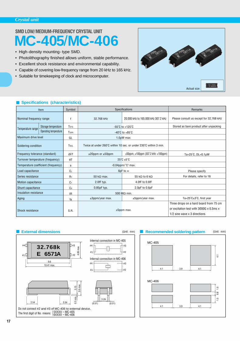
Recommended soldering patternExternal dimensions (Unit: mm)
Internal connection in MC-405
Internal connection in MC-406
(Unit: mm)
#4 #4 #3
#1 #2
#4 #3
#1 #2
#3
#1
2.54 2.54 (0.51) (0.51)
2.29
4.1 3.9 4.1
4.1 3.9 4.1
#2
3.15
1.5
1.5
4.1
0.8
0.2
min
.
3.6
max
.4.
06 m
ax.
9.610.41 max.
32.768k6571AE
Do not connect #2 and #3 of MC-406 to external device.
The first digit of No. means: 5XXXX MC-4056XXXX MC-406
MC-406
MC-405
Crystal unit
SMD LOW/MEDIUM-FREQUENCY CRYSTAL UNIT
MC-405/MC-406• High-density mounting- type SMD.
• Photolithography finished allows uniform, stable performance.
• Excellent shock resistance and environmental capability.
• Capable of covering low-frequency range from 20 kHz to 165 kHz.
• Suitable for timekeeping of clock and microcomputer.
Item
Nominal frequency range
Temperature range
Maximum drive level
Soldering condition
Frequency tolerance (standard)
Turnover temperature (frequency)
Temperature coefficient (frequency)
Load capacitance
Series resistance
Motion capacitance
Shunt capacitance
Insulation resistance
Aging
Shock resistance
Symbol
f
TSTG
TOPR
GL
TSOL
∆f/f
θT
a
CL
R1
C1
C0
IR
fa
S.R.
Specifications
32.768 kHz 20.000 kHz to 165.000 kHz 307.2 kHz
-55˚C to +125˚C
-40˚C to +85˚C
1.0µW max.
Twice at under 260˚C within 10 sec. or under 230˚C within 3 min.
±20ppm or ±50ppm ±50ppm, ±100ppm (307.2 kHz: ±100ppm)
25˚C ±5˚C
-0.04ppm/˚C2 max.
6pF to ∞
50 kΩ max. 55 kΩ to 6 kΩ
2.0fF typ. 4.0fF to 0.6fF
0.85pF typ. 2.0pF to 0.6pF
500 MΩ min.
±3ppm/year max. ±5ppm/year max.
±5ppm max.
Remarks
Please consult us except for 32.768 kHz
Stored as bare product after unpacking
Ta=25˚C, DL=0.1µW
Please specify
For details, refer to 16
Ta=25˚C±3˚C, first year
Three drops on a hard board from 75 cm
or excitation test with 3000G x 0.3ms x
1/2 sine wave x 3 directions
Storage temperatureOperating temperature
Actual size

18
Specifications (characteristics)
Series resistance
Available frequencies from 4.0 MHz to less than 5.5 MHz
D1
L1 L2
B
D2
(Unit: mm)External dimensions
200AM49
Crystal unit
CYLINDER HIGH-FREQUENCY CRYSTAL UNIT
CA-301• Compact design with case as small as 3mm in diameter while
still maintaining excellent characteristics of AT-cut.
• Excellent shock resistance.
• High-stability assured with tight vacuum sealing.
• Capable of covering a frequency range from 4 MHz to 64 MHz.
Item
Nominal frequency range
Temperature range
Drive level
Soldering condition (only lead part)
Frequency tolerance (standard)
Frequency temperature characteristics (standard)
Load capacitance
Series resistance
Shunt capacitance
Insulation resistance
Aging
Shock resistance
Storage temperature
Operating temperature
Maximum drive level
Recommended level
Symbol
f
TSTG
TOPR
GL
DL
TSOL
∆f/f
CL
R1
C0
IR
fa
S.R.
Specifications
4.000 MHz to 30.000 MHz
26.000 MHz to 64.000 MHz
-40˚C to +85˚C
-20˚C to +70˚C
2mW max.
10µW to 100µW
Under 260˚C within 10 sec.
±30ppm
Under 5.5MHz: ±50ppm
Over 5.5MHz: ±30ppm
Fundamental: 10pF to ∞. Over tone: 5pF to ∞
As per below table
5pF max.
500 MΩ min.
±5ppm/year max.
±10ppm max.
∗ 1
Remarks
Fundamental mode
3rd overtone mode
The operating temperature range is -10˚C to 60˚for 5.5MHz and below
Only crystal oscillation is guaranteed
Do not heat the package to more than 150˚C
Ta=25˚C
-10˚C to +60˚C
-20˚C to 70˚C
Please specify
-20˚C to +70˚C, DL=100µW
Ta=25˚C±3˚C, first year
Three drops on a hard board from 75cm height or
excitation test with 3000G x 0.3ms x 1/2 sine wave x 3
directions
∗ 1 8.0 MHz < f < 8.2 MHz: Unavailable.26.000 MHz to 30.000 MHz: standard (3rd overtone mode).
Frequency (MHz)
4.0 ≤ f < 5.5
5.5 ≤ f < 6.0
6.0 ≤ f < 10.0
10.0 ≤ f < 12.0
12.0 ≤ f < 16.0
16.0 ≤ f < 30.0
26.0 ≤ f < 36.0
36.0 ≤ f ≤ 64.0
Series resistance (Ω)
150 Ω max.
100 Ω max.
80 Ω max.
60 Ω max.
50 Ω max.
40 Ω max.
100 Ω max.
80 Ω max.
mode
Fundamental
3rd overtone
Frequency (MHz)
4.000 MHz4.032 MHz4.096 MHz4.190 MHz4.194304 MHz
4.433619 MHz4.500 MHz4.800 MHz4.842673 MHz4.9152 MHz
Model
CA-301Under 5.5 MHzOver 5.5 MHz
L1
10.3 max.8.9 max.
L2
9.5 min.9.5 min.
D1
ø3.1 max.ø3.1 max.
D2
ø0.3ø0.3
B1.11.1
Sample products are without marking.
Actual size

19
Crystal unit
Specifications (characteristics)
Frequency temperature characteristics
Series resistance
D1
L1 L2
B
D2
(Unit: mm)External dimensions
128AU61
CYLINDER HIGH-STABILITY CRYSTAL UNIT
CA-303HS• High-stability in a dia.3mm cylindrical package.
• Small package allows high-density mounting and less weight.
• Excellent shock resistance and environmental capability.
• High-stability with tight vacuum sealing and AT-cut single side
mounting structure.
• Suitable for small telecommunication equipment.
Item
Nominal frequency range
Temperature range
Drive level
Soldering condition
Frequency tolerance (standard)
Frequency temperature characteristics
Load capacitance
Series resistance
Shunt capacitance
Insulation resistance
Aging
Shock resistance
Symbol
f
TSTG
TOPR
GL
DL
TSOL
∆ f/f
CL
R1
C0
IR
fa
S.R.
Specifications
9.600 MHz to 27.000 MHz
-55˚C to +125˚C
-40˚C to +85˚C
2mW max.
10µW to 100µW
240˚C max. within 10sec. and under 200˚C within 40 sec.
±10ppm
As per below table
10pF to ∞
As per below table
3.0pF max.
500 MΩ min.
±1ppm/year max.
±1ppm max.
Remarks
Fundamental mode
Only crystal oscillation is guaranteed
Ta =25˚C ±3˚C,DL=100µW
Please specify
Operable temperature range, DL=100µW
Ta =25˚C ±1˚C, 100µW
Three drops on a hard wooden board from 75 cm or
excitation test with 3000G x 0.3ms x 1/2 sine wave x 3
directions
Temperature range
0˚C to +50˚C
-10˚C to +60˚C
-20˚C to +70˚C
-30˚C to +80˚C
-40˚C to +85˚C
Min. frequency specifications± 3ppm min.± 5ppm min.± 7ppm min.±10ppm min.±15ppm min.
L1
8.9 max.L2
9.5 min.D1
ø3.1 max.D2
ø0.3B
1.1
Sample products are without marking.
Storage temperature
Operating temperature
Maximum drive level
Recommended drive level
Measured values for frequency tolerance and temperature characteristics need to be brought into mutual correlation prior to the start of production. Please see samples.
Frequency (MHz)
9.6 ≤ f < 10.010.0 ≤ f < 12.0
12.0 ≤ f < 16.0
16.0 ≤ f ≤ 27.0
Series resistance (Ω)
50 Ω max.
40 Ω max.
30 Ω max.
25 Ω max.
Actual size

20
Specifications (characteristics)
ø0.3
1.1
8.0 max. 2.0 max.
3.0
max
.
2.5
max
.
1.55
max
.
0.25max. 0.7min.
3.0 6.3 2.4
3.0
1.2
0.6
1.2
Frequency temperature characteristics
Series resistance
(Unit: mm) (Unit: mm)External dimensions Recommended soldering pattern(SA-315HZ)
8.0 max. 7.5 min.
3.0
max
.
1.55
max
.
ø0.31.1
SA-315H
SA-315HZ
128AH72
128AH72
Crystal unit
THIN CYLINDER HIGH-STABILITY CRYSTAL UNIT
SA-315H/315HZ• Thin cylinder of 1.55mm thickness featuring high stability.
• Small and thin with small mounting area and light weight.
• High heat resistance allows reflow soldering.
• Excellent shock resistance and environmental capability.
• Embossed tape usable for SMD.(SA-315HZ)
• Most suitable for small communications devices.
Item
Nominal frequency range
Temperature range
Drive level
Soldering condition
Frequency tolerance (standard)
Frequency temperature characteristics
Load capacitance
Series resistance
Shunt capacitance
Insulation resistance
Aging
Shock resistance
Symbol
f
TSTG
TOPR
TUSE
GL
DL
TSOL
∆ f/f
CL
R1
C0
IR
fa
S.R.
Specifications
10.000 MHz to 27.000 MHz
-55˚C to +125˚C
-40˚C to +85˚C
As per below table
2mW max.
10µW to 100µW
240˚C max. within 10sec. and under 200˚C within 40 sec.
±10ppm
As per below table
10pF to ∞
As per below table
3.0pF max.
500 MΩ min.
±1ppm/Year max.
±1ppm max.
Remarks
Fundamental mode
Specified equivalent series resistance must be satisfied.
Specified equivalent series resistance and frequency-temperature characteristics must be satisfied.
Only crystal oscillation is guaranteed
DL=100µW at Ta=25˚C ±3˚C and specified load capacity.
Please specify
Operable temperature range, DL=100µW
Ta =25˚C ±1˚C, 100µW
Three drops on a hard wooden board from 75 cm or
excitation test with 3000G x 0.3ms x 1/2 sine wave x 3
directions
Operating temperature range
0˚C to +50˚C
-10˚C to +60˚C
-20˚C to +70˚C
-30˚C to +80˚C
-40˚C to +85˚C
Frequency temperature characteristics± 3ppm min.± 5ppm min.± 7ppm min.±10ppm min.±15ppm min.
Storage temperature
Operating temperature
Operable temperature
Maximum drive level
Recommended drive level
Measured values for frequency tolerance and temperature characteristics need to be brought into mutual correlation prior to the start of production. Please see samples.
Frequency (MHz)
10.0 ≤ f < 12.012.0 ≤ f ≤ 27.0
Series resistance (R1)
40 Ω max.
30 Ω max.
Actual size

21
Specifications (characteristics)
Recommended soldering patternExternal dimensions (Unit: mm)
Do not connect #2 and #3 to external device.
Internal connection
(Unit: mm)
#4 #4 #3
#1 #2
#3
#1
0.55.5
(0.9) (0.9)1.9
#2
3.2
2.38
2.54
max
.3.
8 m
ax.
8.0 max.
20.000M572E
1.3
1.9
1.3
1.9
1.3 4.2
Crystal unit
SMALL SMD HIGH - FREQUENCY CRYSTAL UNIT
MA-306• High-density mounting-type SMD.
• Excellent reliability and environment capability.
• Capable of covering a wide frequency range. ( from 17.734 MHz
to 41 MHz)
• 2.54mm thickness is equal to SMD-type IC.
Item
Nominal frequency
Temperature range
Drive level
Soldering condition
Frequency tolerance (standard)
Frequency temperature characteristics(standard)
Load capacitance
Series resistance
Shunt capacitance
Insulation resistance
Aging
Shock resistance
Symbol
f
TSTG
TOPR
GL
DL
TSOL
∆ f/f
CL
R1
C0
IR
fa
S.R.
Specifications
17.734 MHz to 41.000 MHz
-55˚C to +100˚C
-20˚C to +70˚C
2mW max.
10µW to 100µW
Twice at under 260˚C within 10 sec.
or under 230˚C within 3 min.
±50ppm
±30ppm
10pF to ∞
60 Ω max.
5pF max.
500 MΩ min.
±5ppm/Y max.
±10ppm max.
Remarks
Fundamental mode
Stored as bare product after unpacking
Only crystal oscillation is guaranteed
Ta=25˚C±3˚C
-20˚C to +70˚C
Please specify
-20˚C to +70˚C, DL=100µW
Ta=25˚C±3˚C, first year
Three drops on a hard board from 75 cm or excitation
test with 3000G x 0.3ms x 1/2 sine wave x 3 directions
Storage temperature
Operating temperature
Maximum drive level
Recommended drive level
Actual size

22
Specifications (characteristics)
Recommended soldering patternExternal dimensions (Unit: mm)
Internal connection
(Unit: mm)
#4 #4 #3
#1 #2
#3
#1
0.79.6
(1.2) (1.2)
2.1
#2
4.0
3.5
0.5
3.7
max
.4.
8 m
ax.
11.7 max.
20.000M572E
1.8
1.9
1.7
1.9
1.8 7.8
Crystal unit
SMD HIGH-FREQUENCY CRYSTAL UNIT
MA-406• High-density mounting-type SMD.
• Excellent heat-resistance and environment capability.
• Cover a wide frequency range, from 4 MHz to 64 MHz.
Item
Nominal frequency
Temperature range
Drive level
Soldering condition
Frequency tolerance (standard)
Frequency temperature characteristics(standard)
Load capacitance
Series resistanceShunt capacitanceInsulation resistanceAging
Shock resistance
Symbol
f
TSTG
TOPR
GL
DL
TSOL
∆ f/f
CL
R1
C0
IR
fa
S.R.
Specifications
4.000 MHz to 30.000 MHz
26.000 MHz to 64.000 MHz
-55˚C to +125˚C
-20˚C to +70˚C
2mW
10µW to 100µW
Twice at under 260˚C within 10 sec.
or under 230˚C within 3 min.
±50ppm
Under 5.5 MHz: ±50ppm
Over 5.5 MHz: ±30ppm
Fundamental: 10pF to ∞
Over tone: 5pF to ∞
As per table below
5pF max.
500 MΩ min.
±5ppm/year
±10ppm max.
∗ 1
Remarks
Fundamental mode
3rd overtone mode
Stored as bare product after unpacking
Only crystal oscillation is guaranteed
Ta=25˚C±3˚C
-20˚C to +70˚C
Please specify
-20˚C to +70˚C, DL=100µW
Ta=25˚C±3˚C, first year
Three drops on a hard board from 75 cm or excitation
test with 3000G x 0.3ms x 1/2 sine wave x 3 directions
∗ 1 8.0 MHz < f < 8.2 MHz: Unavailable. For frequencies below 5.5 MHz, see "Avallable frequencies form 4.0 MHz to less than 5.5 MHz" on page 18.26.000 MHz to 30.000 MHz: standard (3rd overtone mode).
Frequency (MHz)
Series resonanceresistance (Ω)
Mode
4.0 ≤ f < 5.5
150 Ω max.
5.5 ≤ f < 6.0
100 Ω max.
6.0 ≤ f < 10.0
80 Ω max.
10.0 ≤ f < 12.0
60 Ω max.
12.0 ≤ f < 16.0
50 Ω max.
16.0 ≤ f < 30.0
40 Ω max.
26.0 ≤ f ≤ 36.0
100 Ω max.
36.0 < f ≤ 64.0
80 Ω max.
Fundamental mode 3rd overtone mode
Storage temperature
Operating temperatureMaximum drive level
Recommended drive level
Do not connect #2 and #3 external device.
Actual size

23
Specifications (characteristics)
Recommended soldering patternExternal dimensions
Frequency temperature characteristics
(Unit: mm)
Internal connection
(Unit: mm)
#4 #4 #3
#1 #2
#3
#1
0.79.6
(1.2) (1.2)
2.1
#2
4.0
3.5
0.5
3.7
max
.4.
8 m
ax.
11.7 max.
20.000MH51AE
1.8
1.9
1.7
1.9
1.8 7.8
Series resistance
Crystal unit
SMD HIGH-STABILITY CRYSTAL UNIT
MA-406H• High-density mounting-type SMD.
• Excellent heat-resistance and environment capability.
• 9.6 MHz to 27.0 MHz available.
Item
Nominal frequency range
Temperature range
Drive level
Soldering condition Frequency tolerance (standard)Frequency temperature characteristicsLoad capacitanceSeries resistanceShunt capacitanceInsulation resistanceAging
Shock resistance
Specifications
9.600 MHz to 27.000 MHz
-55˚C to +125˚C
-40˚C to 85˚C
2mW max.
10µW to 100µW
240˚C max. within 10 sec. and under 200˚C within 40 sec.±10ppm
As per below table
10pF to ∞
As per below table
5.0pF max.
500 MΩ min.
±1ppm/year max.
±1ppm max.
Symbol
f
TSTG
TOPR
GL
DL
TSOL
∆ f/f
CL
R1
C0
IR
fa
S. R.
Remarks
Fundamental mode
Stored as bare product after unpacking
Only crystal oscillation is guaranteed
Ta=25˚C±3˚C,DL=100µW
Please specify
Operable temperature range, DL=100µW
Ta=25˚C ±1˚C, DL=100µW
Three drops on a hard wooden board from 75 cm orexcitation test with 3000G x 0.3ms x 1/2 sine wave x 3directions
Temperature range
0˚C to +50˚C
-10˚C to +60˚C
-20˚C to +70˚C
-30˚C to +80˚C
-40˚C to +85˚C
Min. frequency specifications
± 3ppm min.
± 5ppm min.
± 7ppm min.
±10ppm min.
±15ppm min.
Storage temperatureOperable temperature
Maximum drive level
Recommended drive level
Measured values for frequency tolerance and temperature characteristics need to be brought into mutual correlation prior to the start of production. Please see samples.
Frequency (MHz)
9.6 ≤ f < 10.0
10.0 ≤ f < 12.0
12.0 ≤ f < 16.0
16.0 ≤ f ≤ 27.0
Series resistance (Ω)
50 Ω max.
40 Ω max.
30 Ω max.
25 Ω max.
Do not connect #2 and #3 external device.
Actual size

24
Specifications (characteristics)
Recommended soldering patternExternal dimensions (Unit: mm) (Unit: mm)
#4 #3
#1
2.54 2.54 1.09 1.093.30
#2
4.19
4.6
max
.0.
2 m
in.
5.08
max
.
13.46 max.
12.70
20.000M5251AE
Internal connection in MA-505
Internal connection in MA-506
#4 #3
#1 #2
#4 #3
#1 #2
Do not connect #2 and #3 of MA-506 to external device.
The first digit of lot No. means: 5XXXX MA-5056XXXX MA-506
4.1 7.0 4.1
4.1 7.0 4.1
2.1
2.1
5.6
1.5
MA-506
MA-505
Crystal unit
SMD HIGH-FREQUENCY CRYSTAL UNIT
MA-505/MA-506• High-density mounting-type SMD.
• Excellent heat-resistance and environment capability.
• Capable of covering a wide range of frequency range from 4.0 MHz
to 64 MHz.
Item
Nominal frequency range
Temperaturerange
Drive level
Soldering condition
Frequency tolerance (standard)
Frequency temperature characteristics(standard)
Load capacitance
Series resistance
Shunt capacitance
Insulation resistance
Aging
Shock resistance
Symbol
f
TSTG
TOPR
GL
DL
TSOL
∆f/f
CL
R1
C0
IR
fa
S. R.
Specifications
4.000 MHz to 30.000 MHz ∗ 1
26.000 MHz to 64.000 MHz
-55˚C to +125˚C
-20˚C to +70˚C
2mW max.
10µW to 100µW
Twice at under 260˚C within 10 sec.or under 230˚C within 3 min.
±50ppm
Under 5.5 MHz: ±50ppm
Over 5.5 MHz: ±30ppm
Fundamental: 10pF to ∞. Over tone: 5pF to ∞
As per below table
5pF max.
500 MΩ min.
±5ppm/year max.
±10ppm max.
Remarks
Fundamental mode
3rd overtone mode
Stored as bare product after unpacking
Only crystal oscillation is guaranteed
Ta=25˚C±3˚C, DL=100µW
-20˚C to +70˚C, DL=100µW
Please specify
-20˚C to +70˚C, DL=100µW
Ta=25˚C±3˚C, first year
Three drops on a hard board from 75 cm or excitationtest with 3000G x 0.3ms x 1/2 sine wave x 3directions
∗ 1 8.0 MHz < f < 8.2 MHz: Unavailable. For frequencies below 5.5 MHz, see "Available frequencies from 4.0 MHz to less than 5.5 MHz" on page 18.26.000 MHz to 30.000 MHz: standard (3rd overtone mode).
Frequency (MHz)
Series resonanceresistance (Ω)
Mode
4.0 ≤ f < 5.5
150 Ω max.
5.5 ≤ f < 6.0
100 Ω max.
6.0 ≤ f < 10.0
80 Ω max.
10.0 ≤ f < 12.0
60 Ω max.
12.0 ≤ f < 16.0
50 Ω max.
16.0 ≤ f < 30.0
40 Ω max.
26.0 ≤ f ≤ 36.0
100 Ω max.
36.0 < f ≤ 64.0
80 Ω max.
3rd overtone modeFundamental mode
Storage temperatureOperating temperature
Maximum drive levelRecommended drive level
Actual size

25
Specifications (characteristics)
Recommended soldering patternExternal dimensions (Unit: mm) (Unit: mm)
1.4
max
.3.
5±0.
2
6.0±0.2
Internal connection
[ Top View ]
FA-368
FA-367
FA-365
# 1 # 2
# 4
# 1
# 4
# 1
# 3
# 2
# 3
# 2
1.9 1.9
2.4
2.5
1.4
1.4
2.6
1.9 1.92.6
FA-365
FA-367/ 368
2 0 . 0 0 0E 56XR
Crystal unit
THIN SMD HIGH-FREQUENCY CRYSTAL UNIT
FA-365/367/368• High-density mounting-type SMD.
• Excellent reliability and environment capability.
• Capable of covering a wide frequency range. (from 14 MHz to
41 MHz)
• 1.4mm thickness is equal to SMD-type IC.
Item
Nominal frequency range
Temperature range
Drive level
Soldering condition
Frequency tolerance (standard)
Frequency temperature characteristics(standard)
Load capacitance
Series resistance
Shunt capacitance
Insulation resistance
Aging
Shock resistance
Specifications
14.000 MHz to 41.000 MHz
-55˚C to +125˚C
-20˚C to +70˚C
2mW max.
10µW to 100µW
Twice at under 260˚C within 10 sec.or under 230˚C within 3 min.
±50ppm, ±100ppm
±30ppm
10pF to ∞
50 Ω max.
5.0pF max.
500 MΩ min.
±5ppm/year max.
±10ppm max.
Symbol
f
TSTG
TOPR
GL
DL
TSOL
∆ f/f
CL
R1
C0
IR
fa
S. R.
Remarks
Fundamental mode
Stored as bare product after unpacking
Only crystal oscillation is guaranteed
Ta=25˚C±3˚C
-20˚C to +70˚C
Please specify
-20˚C to +70˚C,DL=100µw
Ta=25˚C ±3˚C, first year
Three drops on a hard board from 75 cm or excitationtest with 3000G x 0.3ms x 1/2 sine wave x 3 directions
Storage temperature
Operating temperature
Maximum drive level
Recommended drive level
Actual size

26
#1 #2 #3
2.1
4.6 max.
0.25
(7.5
)(1
.3)
8.8
max
.7.
0
2.54 2.54
16.0 max.
Specifications (characteristics)
Output frequency table
Output frequency example
External dimensions (Unit: mm)
SG-10 BE32.768 KHz
0131A
No.123
Pin terminalGNDOUTVDD
Crystal oscillator
SIP LOW/MEDIUM-FREQUENCY CRYSTAL OSCILLATOR
SG-10• Low current consumption.
• Small suited to high-density mounting.
• Mountable on a standard printed circuit board.
• Cylindrical low/medium-frequency crystal unit builtin, thus
assuring high reliability.
Item
Output frequency range
Power source voltage
Temperature range
Soldering condition (lead part)Frequency tolerance
Frequency temperature characteristics
Frequency voltage characteristics
Current consumption
Duty
Output voltage
Output load condition (fan out)
Output rise time
Output fall time
Oscillation start up time
Aging
Shock resistance
Symbol
f0
VDD-GND
VDD
TSTG
TOPR
TSOL
∆f/f0
lOP
tW/t
VOH
VOL
N/CL
tTLH
tTHL
tOSC
fa
S.R.
Max. supply voltageOperating voltage
Specifications
10.0000 Hz to 153.6000 kHz
-0.3V to +7.0V
4.5V to 5.5V
-55˚C to +125˚C
-10˚C to +70˚C
Under 260˚C within 10 sec.
A: ±10ppm B: ±50ppm
+10ppm / -120ppm
±10ppm max.
0.5mA max.
40% to 60%(except for cases of 1/3 and 1/5 divided frequency.)
VDD -1.0V min.
0.4V max.
1TTL max./15pF max.
60ns max.
50ns max.
1 s max.
±5ppm/year max.
±10ppm max.
Remarks
For output frequency, see the table below
Do not heat the package to more than 150˚C
VDD=5V Ta=25˚C
-10˚C to +70˚C, taking Ta=25˚C as the reference
No load condition
1/2 VDD or 1.4V level
IOH= -40µA
IOL=1.6mA
TTL load/C-MOS load
Refer to output waveform (page 11)
For more than 1ms until VDD=0V→4.5V.
Time at 4.5V to be 0 sec.
Ta=25˚C ±3˚C, VDD=5V, first year
Three drops on a hard board from 75 cm or excitationtest with 3000G x 0.3ms x 1/ 2 sine wave in 3directions
Unless otherwise stated, characteristics (specifications) shown in the above table are based on the rated operating temperature and voltage condition.
Oscillation source
Divided frequencyoutput (calculation method)
Oscillation source
Divided frequency
32.768 kHz,60.000 kHz, 96.000 kHz, 100.000 kHz,
153.600 kHz
Oscillation source frequency x (any arbitrary one of 1/1, 1/2, 1/3,1/4, 1/5, 1/6, 1/12 x (any arbitrary one of 1/1, 1/10, 1/100,1/1000). Over 10.0 Hz range.
For frequencies other than the above, please consult us. (min. order lot 10,000 pcs.)
32.768 kHz , 60.000 kHz , 96.000 kHz, 100.000 kHz ,153.600 kHz
10.000 Hz , 50.000 Hz , 100.000 Hz , 1.000 kHz, 4.800 kHz , 9.600 kHz, 19.200 kHz , 38.400 kHz,
50.000 kHz , 76.800 kHz
Storage temperatureOperating temperature
Actual size

27
#1 #2 #3
2.1
4.6 max.
0.25
(7.5
)(1
.3)
8.8
max
.7.
0
2.54 2.54
16.0 max.
Specifications (characteristics)
Output frequency example External dimensions (Unit: mm)
Output frequency
No.123
Pin terminalGNDOUTVDD
SG-11 CE6.1440 MHz
6071B
Crystal oscillator
SIP HIGH-FREQUENCY CRYSTAL OSCILLATOR
SG-11• Use of C-MOS IC allows low current consumption.
• Small suited to high-density mounting.
• Mountable on a standard printed board.
• Cylindrical AT-cut crystal unit builtin, thus assuring high
reliability.
Item
Output frequency range
Power source voltage
Temperature range
Soldering condition (lead part)
Frequency stability
Current consumption
Duty
Output voltage
Output load condition (fan out)
Output rise time
Output fall time
Oscillation start up time
Aging
Shock resistance
Symbol
f0
VDD-GND
VDD
TSTG
TOPR
TSOL
∆f/f0
IOP
tw/t
VOH
VOL
N/CL
tTLH
tTHL
tOSC
fa
S.R.
Specifications
1.5 MHz to 24.0000 MHz
-0.3V to +7.0V
4.5V to 5.5V
-55˚C to +125˚C
-10˚C to +70˚C
Under 260˚C within 10 sec.
C: ±100ppm
10mA max.
40% to 60%
VDD -0.4V min.
0.4V max.
1TTL max./15pF max.
20ns max.
15ns max.
10ms max.
±10ppm max. (3ppm typ.)
±10ppm max.
Remarks
For output frequency, refer to the table below
Do not heat the package to more than 150˚C
-10˚C to +70˚C
No load condition
1/2 VDD or 1.4V level
IOH=-40µA
IOL=1.6mA
TTL load /C-MOS load
Refer to output waveform (page 11)
For more than 1ms until VDD =0V→4.5V
Time at 4.5V to be 0 sec.
Ta=25˚C ±3˚C, VDD=5V, first year
Three drops on a hard board from 75 cm or excitation
test with 3000G x 0.3ms x 1/2 sine wave x 3 directions
Unless otherwise stated, characteristics (specifications) shown in the above table are based on the rated operating temperature and voltage condition.
3.579545 MHz
4.0000 MHz
4.9152 MHz
6.1440 MHz
8.0000 MHz
9.8304 MHz
12.0000 MHz
14.31818 MHz
16.0000 MHz
18.4320 MHz
19.6608 MHz
20.0000 MHz
24.0000 MHz
Max. supply voltageOperating voltage
Storage temperatureOperating temperature
Actual size

28
Crystal oscillator
#14 #8
#1 #1 #4
#8 #5
#7
5.3
max
.2.
54 m
in.
0.2
min
.
0.2
min
.
6.36
No.178
14
Pin terminalOE
GNDOUTVDD
No.1458
Pin terminalOE
GNDOUTVDD
External dimensions
SG-51 series
Specifications (characteristics)
(Unit: mm)
SG51PH 6052AESG531P C
32.0000MHz C20.0000M
6050AE
5.3
max
.2.
54 m
in.
15.24 7.62
0.510.25 0.25
90˚ to105˚
90˚ to105˚
7.62 7.62
19.8 max. 13.7 max.
6.6
SG-531 series
FULL-SIZE DIP HIGH-FREQUENCY CRYSTAL OSCILLATOR
SG-51 series
Item
Output frequency range
Power source voltage
Temperature rangeSoldering condition (lead part)
Frequency stability
Current consumption
Duty
Output voltage
Output loadcondition (fan out)
Output enable/disable input voltage
Output disable currentOutput rise timeOutput fall time
Oscillation start up time
Aging
Shock resistance
Symbol
f0
VDD-GNDVDD
TSTG
TOPR
TSOL
∆f/f0
Iop
tw/t
VOH
(IOH)VOL
(IOL)
CL
NVIH
VIL
IOE
tTLH
tTHL
tOSC
fa
S.R.
HALF-SIZE DIP HIGH-FREQUENCY CRYSTAL OSCILLATOR
SG-531 series
C-MOS levelTTL level
C-MOS levelTTL levelC-MOS levelTTL level
C-MOSTTL
SG-51P/531P SG-51PTJ/531PTJ SG-51PH/531PH
Specifications
26.0001 MHz to 66.6667 MHz
-0.3V to +7.0V5.0V±0.5V
-55˚C to +125˚C -55˚C to +100˚C-10˚C to +70˚C
Under 260˚C within 10 sec.B: ± 50ppmC: ±100ppm
23mA max. 35mA max.40% to 60% — 40% to 60%
45% to 55% —-0.4V min. 2.4V min. VDD -0.4V min.
-400µA -4mA0.4V max.
16mA 8mA 4mA50pF max. — 50pF max.
10TTL max. 5TTL max. —2.0V min. 3.5V min. 2.0V min.0.8V max. 1.5V max. 0.8V max.
12mA max. 28mA max. 20mA max.
8ns max.
8ns max.
4ms max. 10ms max.
±5ppm/year max.
±20ppm max.
Remarks
Don't heat the package to more than 150˚C-10˚C to +70˚C
B type is possible up to 55.0 MHzNo load condition
1/2 VDD level1.4V level
IIH=1µA max. (OE=VDD)IIL= -100µA min. (OE=GND), PTJ: -500µA
OE=GNDC-MOS load: 20%→80% VDD
TTL load: 0.4V→2.4VC-MOS load: 80%→20% VDD
TTL load: 2.4V→0.4V
More than for 1ms until VDD =0V→4.5VTime at 4.5V to be 0 sec.
Ta=25˚C, VDD =5V,first year
Three drops on a hard board from 75 cm orexcitation test with 3000G x 0.3ms x 1/2 sinewave in 3 directions
Note: • Unless otherwise stated, characteristics (specifications) shown in the above table are based on the rated operating temperature and voltage condition.• External by-pass capacitor is recommended.
Max. supply voltageOperating voltageStorage temperatureOperating temperature
1.0250 MHz to 26.0000 MHz
—5ns max.
—5ns max.
7ns max.—
7ns max.—
• Pin compatible with half-size metal can.Common
• Cylindrical AT-cut crystal unit builtin, thus assuring high reliability.
• Use of C-MOS IC enables reduction of current consumption.
• Pin compatible with full-size metal can.
Actual size

29
Crystal oscillator
Recommended soldering pattern (Unit: mm)
1.3
3.0
5.8
3.0
1.3 3.8
#1 #2
#4 #3
8.65
0.25
9.8
max
4.7
max
.
4.06
0.25
min
.
No.1234
Pin terminalOE
GNDOUTVDD
External dimensions
Specifications (characteristics)
(Unit: mm)
14.0 max.
5.08 7.620.51
20.0000MSG-615P C
6100AE
SMD HIGH-FREQUENCY CRYSTAL OSCILLATOR
SG-615 series
Item
Output frequency range
Power source voltage
Temperature range
Soldering condition
Frequency stabilityCurrent consumption
Duty
Output voltage
Output loadcondition (fan out)
Output enable/disable input voltage
Output disable current
Output rise time
Output fall time
Oscillation start up time
Aging
Shock resistance
Symbol
f0
VDD-GNDVDD
TSTG
TOPR
TSOL
∆f/f0
Iop
tw/t
VOH
(IOH)VOL
(IOL)CL
NVIH
VIL
IOE
tTLH
tTHL
tOSC
fa
S.R.
C-MOS levelTTL level
C-MOSTTL
C-MOS levelTTL levelC-MOS levelTTL level
SG-615P SG-615PTJ SG-615PH
Specifications
1.0250 MHz to 26.0000 MHz 26.0001 MHz to 66.6667 MHz
-0.3V to +7.0V5.0V±0.5V
-55˚C to +125˚C-10˚C to 70˚C (-40˚C to 85˚C)
Twice at under 260˚C within 10 sec.or under 230˚C within 3 min.
B: ±50ppmC: ±100ppm
23mA max. 35mA max.40% to 60% — 40% to 60%
45% to 55% —VDD -0.4V min. 2.4V min. VDD -0.4V min.
-4mA0.4V max.
16mA 8mA 4mA50pF max. — 50pF max.
10TTL max. 5TTL max. —2.0V min. 3.5V min. 2.0V min.0.8V max. 1.5V max. 0.8V max.
12mA max. 28mA max. 20mA max.
4ms max. 10ms max.
±5ppm/year max.
±20ppm max.
8ns max.
—5ns max.
—5ns max.
7ns max.—
7ns max.—
Remarks
Stored as bare product after unpacking
B type is possible up to 55 MHz
No load conditionC-MOS load: 1/2VDD
TTL load: 1.4V
IIH=1µA max.(OE=VDD)IIL=-100µA min.(OE=GND) IIL=-500µA min.(OE=GND) PTJ
OE=GND
C-MOS load: 20%→80% VDD
TTL load: 0.4V→2.4V
C-MOS load: 80%→20% VDD
TTL load: 2.4V→0.4V
Time at 4.5V to be 0 sec.
Ta= 25˚C, VDD = 5V, first year
Three drops on a hard board from 75 cm orexcitation test with 3000G x 0.3ms x 1/2sinewave in 3 directions
Note: • Unless otherwise stated, characteristics (specifications) shown in the above table are based on the rated operating temperature and voltage condition.• External by-pass capacitor is recommended.
Max. supply voltageOperating voltageStorage temperatureOperating temperature
-400µA
• High-density mounting-type SMD.
• A general-purpose SMD with heat-resisting cylindrical AT-cut
crystal unit and allowing almost the same soldering temperature
as SMD IC.
• Cylindrical AT crystal unit builtin, thus assuring high reliability.
• Provided with output enable function.
• Low current consumption. Actual size
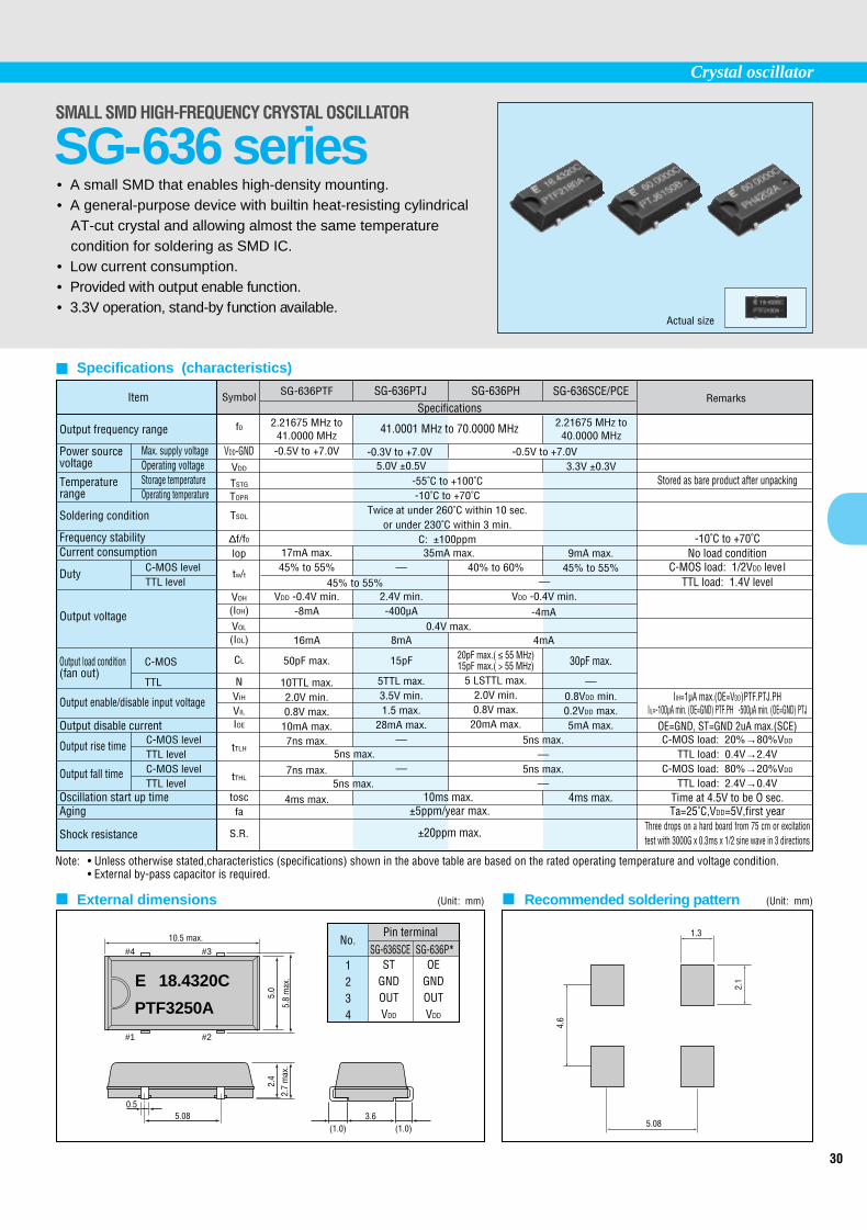
30
Crystal oscillator
#4 #3
#1
0.55.08
1.3
5.08(1.0) (1.0)3.6
#2
5.0
4.6
2.1
2.4
2.7
max
.5.
8 m
ax.
10.5 max.
1234
STGNDOUTVDD
OEGNDOUTVDD
Recommended soldering pattern External dimensions
Specifications (characteristics)
(Unit: mm)(Unit: mm)
18.4320CE
PTF3250A
Pin terminalNo.
SG-636PSG-636SCE ∗∗
SMALL SMD HIGH-FREQUENCY CRYSTAL OSCILLATOR
SG-636 series
Item
Output frequency range
Power sourcevoltage
Temperaturerange
Soldering condition
Frequency stabilityCurrent consumption
Duty
Output voltage
Output load condition(fan out)
Output enable/disable input voltage
Output disable current
Output rise time
Output fall time
Oscillation start up timeAging
Shock resistance
Max. supply voltageOperating voltageStorage temperatureOperating temperature
C-MOS levelTTL level
C-MOS
TTL
C-MOS levelTTL levelC-MOS levelTTL level
Symbol
f0
VDD-GNDVDD
TSTG
TOPR
TSOL
∆f/f0
lop
tw/t
VOH
(IOH)
VOL
(IOL)
CL
NVIH
VIL
IOE
tTLH
tTHL
toscfa
S.R.
SG-636PTF SG-636PTJ SG-636PHSpecifications
41.0001 MHz to 70.0000 MHz2.21675 MHz to41.0000 MHz-0.5V to +7.0V
Remarks
-55˚C to +100˚C-10˚C to +70˚C
Twice at under 260˚C within 10 sec.or under 230˚C within 3 min.
C: ±100ppm17mA max.45% to 55%
VDD -0.4V min.-8mA
16mA
50pF max.
10TTL max.2.0V min.0.8V max.
10mA max.7ns max.
7ns max.
4ms max.
35mA max.—
2.4V min.-400µA
8mA
15pF
5TTL max.3.5V min.1.5 max.
28mA max.—
—
40% to 60%
20pF max.( ≤ 55 MHz)15pF max.( > 55 MHz)
5 LSTTL max.2.0V min.0.8V max.
20mA max.
Stored as bare product after unpacking
-10˚C to +70˚CNo load condition
C-MOS load: 1/2VDD leve lTTL load: 1.4V level
IIH=1µA max.(OE=VDD)PTF.PTJ.PHIIL=-100µA min. (OE=GND) PTF.PH -500µA min. (OE=GND) PTJ
OE=GND, ST=GND 2uA max.(SCE)C-MOS load: 20%→80%VDD
TTL load: 0.4V→2.4VC-MOS load: 80%→20%VDD
TTL load: 2.4V→0.4VTime at 4.5V to be O sec.Ta=25˚C,VDD=5V,first year
Three drops on a hard board from 75 cm or excitationtest with 3000G x 0.3ms x 1/2 sine wave in 3 directions
10ms max.±5ppm/year max.
±20ppm max.
Note: • Unless otherwise stated,characteristics (specifications) shown in the above table are based on the rated operating temperature and voltage condition.• External by-pass capacitor is required.
-0.5V to +7.0V
45% to 55%
5ns max.
5ns max.
• A small SMD that enables high-density mounting.• A general-purpose device with builtin heat-resisting cylindrical
AT-cut crystal and allowing almost the same temperaturecondition for soldering as SMD IC.
• Low current consumption. • Provided with output enable function.• 3.3V operation, stand-by function available.
SG-636SCE/PCE
-0.3V to +7.0V5.0V ±0.5V
2.21675 MHz to40.0000 MHz
3.3V ±0.3V
9mA max.45% to 55%
30pF max.
—0.8VDD min.0.2VDD max.5mA max.
—VDD -0.4V min.
0.4V max.
4ms max.
Actual size
5ns max.—
5ns max.—
-4mA
4mA

31
Crystal oscillator
Duty of SG-51,531,615 and 636 series
REFERENCE DATA
Current consumption of SG-51,531,615 and 636 series (typical)
By-pass capacitor
10 20 30 40 50 60 70 8000
5
10
15
20
25
30
35
SG-P series
Black line: VDD=5VBlue line: VDD=3.3V
SG-PTJ series SG-PH series
SG-636PTF series
Output frequency (MHz)
Curr
ent c
onsu
mpt
ion
(mA)
SG-636PCE/SG-636SCE series
Output pattern
GND pattern
VDD pattern
Circuit configuration sample
1.025M2.2167M 16.0M 21.026M 26.0M 40.0M
FrequencyLoadModel
66.67M 70M
Duty 45%,55%Duty 40%,60%
possible dependingon load condition.
..........Duty 45%,55%
(Ta=25˚C,and no-load)
CL=15pF max.
OUT
NC GND
oscillator
VDD
GND
load
VDD
SG-51P/SG-531P/SG-615P
SG-51PTJ/SG-531PTJ/SG-615PTJ
SG-51PH/SG-531PH/SG-615PH
SG-636PTF
SG-636PTJ
SG-636PH
SG-636PCE/SG-636SCE
TTL
C-MOS
TTL
C-MOS
TTL
C-MOS
TTL
C-MOS
∗ 1 Duty 45% to 55% of SG-615 is guaranteed in an operating temperature range of from -10 to +70˚C.
∗ 2 Common conditions for all products.
(1) Line impedance of a power supply should be minimized by VDD and GND patterns.
(2) A 0.01µF power supply by-pass capacitor should be installed very close to an oscillator.
(3) Output load should be as close as possible to an oscillator (within 20mm).(4) Power supply range: operating voltage.(5) 10 TTL: RL ≥ 390 Ω, CL ≤ 15pF.
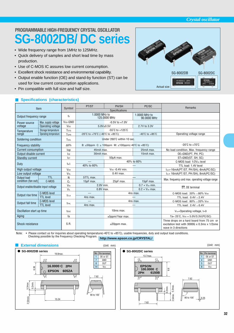
32
Crystal oscillator
(Unit: mm)
5.3m
ax.
0.2m
in.
0.25
7.62
2.54
min
.
7.62
# 4# 1
# 5# 8
13.7max.
6.6100.0000 C
6150B
EPSON
2PH
No.1458
OE or STGNDOUTVDD
No.17814
OE or STGNDOUTVDD
90 to 105˚90 to 105˚
External dimensions
Specifications (characteristics)
(Unit: mm)
Pin terminalPin terminal19.8max.
6.36
2.54
min
.5.
3max
.
0.2m
in.
15.24
7.62
# 14 # 8
# 1 # 7
6052A16.0000 CEPSON
2PH
SG-8002DB series SG-8002DC series
PROGRAMMABLE HIGH-FREQUENCY CRYSTAL OSCILLATOR
SG-8002DB/ DC series
Item
Output frequency range
Power source voltage
Temperature range
Soldering condition
Frequency stabilityCurrent consumptionOutput disable currentStandby current
Duty
High output voltageLow output voltageOutput loadcondition (fan out)
Output enable/disable input voltage
Output rise time
Output fall time
Oscillation start up time
Aging
Shock resistance
Symbol
f0
VDD-GNDVDD
TSTG
TOPR
TSOL
∆f/f0
IopIOE
IST
tw/t
VOH
VOL
NCL
VIH
VIL
tTLH
tTHL
tOSC
fa
S.R.
TTLC-MOS
C-MOS levelTTL levelC-MOS levelTTL level
PT/ST PH/SH PC/SCSpecifications
-0.5V to +7.0V5.0V±0.5V 2.7V to 3.3V
-55˚C to +125˚C-20˚C to +70˚C (-40˚C to +85˚C) -40˚C to +85˚C
Under 260˚C within 10 sec.
B: ±50ppm C: ± 100ppm M: ±100ppm(-40˚C to +85˚C)
45mA max. 25mA max.30mA max. 15mA max.
— 40% to 60%40% to 60% —
VDD -0.4V min.0.4V max.
5TTL max. —15pF max. 25pF max. 15pF max.
2.0V min. 0.7 × VDD min.0.8V max. 0.2 × VDD max.
— 4ns max.4ns max. —
— 4ns max.4ns max. —
10ms max.
±5ppm/Year max.
±20ppm max.
Remarks
Operating voltage range
-20˚C to +70˚C
No load condition, Max. frequency rangeOE=GND(PT, PH, PC)ST=GND(ST, SH, SC)
C-MOS load: 1/2VDD levelTTL load: 1.4V level
IOH=-16mA(PT /ST, PH/SH),-8mA(PC/SC)IOL= 16mA(PT /ST, PH /SH), 8mA(PC/SC)
Max. frequency and max. operating voltage range
ST_
, OE terminal
C-MOS load: 20%→80% VDD
TTL load: 0.4V→2.4V
C-MOS load: 80%→20% VDD
TTL load: 2.4V→0.4V
VDD=Operating voltage, t=0
Ta= 25˚C, VDD = 5.0V/3.3V(PC/SC)
Three drops on a hard board from 75 cm orexcitation test with 3000G x 0.3ms x 1/2sinewave in 3 directions
Note: • Please contact us for inquiries about operating temperature(-40˚C to +85˚C), usable frequencies, duty and output load conditions.Checking possible by the Frequency Checking Program.
Max. supply voltageOperating voltageStorage temperatureOperating temperature
50µA max.
• Wide frequency range from 1MHz to 125MHz.• Quick delivery of samples and short lead time by mass
production.• Use of C-MOS IC assures low current consumption.• Excellent shock resistance and environmental capability.• Output enable function (OE) and stand-by function (ST) can be
used for low current consumption applications.• Pin compatible with full size and half size.
1.0000 MHz to 125.0000 MHz
1.0000 MHz to 90.0000 MHz
Actual size
http://www.epson.co.jp/CRYSTAL/
SG-8002DB SG-8002DC

33
Crystal oscillator
8.65
0.25
9.8
max
.4.
7 m
ax.
4.06
0.25
min
.
1.52
5.08 7.620.51
14.0 max.
Recommended soldering pattern (Unit: mm)
100.0000 C7100A
EPSON
2PH
No.1234
OE or STGNDOUTVDD
1.3 3.8 1.3
3.0
5.8
3.0
External dimensions
Specifications (characteristics)
(Unit: mm)
Pin terminal
# 3# 4
# 2# 1
PROGRAMMABLE HIGH-FREQUENCY CRYSTAL OSCILLATOR
SG-8002JA series
Item
Output frequency range
Power source voltage
Temperature range
Soldering condition
Frequency stabilityCurrent consumptionOutput disable currentStandby current
Duty
High output voltageLow output voltageOutput loadcondition (fan out)
Output enable/disable input voltage
Output rise time
Output fall time
Oscillation start up time
Aging
Shock resistance
Symbol
f0
VDD-GNDVDD
TSTG
TOPR
TSOL
∆f/f0
IopIOE
IST
tw/ t
VOH
VOL
NCL
VIH
VIL
tTLH
tTHL
tOSC
fa
S.R.
TTLC-MOS
C-MOS levelTTL levelC-MOS levelTTL level
PT/ST PH/SH PC/SCSpecifications
-0.5V to +7.0V5.0V±0.5V 2.7V to 3.6V
-55˚C to +125˚C-20˚C to +70˚C (-40˚C to +85˚C) -40˚C to +85˚C
Twice at under 260˚C within 10 sec.or under 230˚C within 3 min.
B: ±50ppm C: ± 100ppm M: ±100ppm(-40˚C to +85˚C)
45mA max. 25mA max.30mA max. 15mA max.
— 40% to 60%40% to 60% —
VDD -0.4V min.0.4V max.
5TTL max. —15pF max. 25pF max. 15pF max.
2.0V min. 0.7 × VDD min.0.8V max. 0.2 × VDD max.
— 4ns max.4ns max. —
— 4ns max.4ns max. —
10ms max.
±5ppm/year max.
±20ppm max.
Remarks
Operating voltage range
-20˚C to +70˚C
No load condition, Max. frequency rangeOE=GND(PT, PH, PC)ST=GND(ST, SH, SC)
C-MOS load: 1/2VDD levelTTL load: 1.4V level
IOH=-16mA(PT /ST, PH/SH),-8mA(PC/SC)IOL= 16mA(PT /ST, PH /SH), 8mA(PC/SC)
Max. frequency and max. operating voltage range
ST_
, OE terminal
C-MOS load: 20%→80% VDD
TTL load: 0.4V→2.4V
C-MOS load: 80%→20% VDD
TTL load: 2.4V→0.4V
Time at operating voltage to be 0 sec.
Ta= 25˚C, VDD = 5.0V/3.3V(PC/SC)
Three drops on a hard board from 75 cm orexcitation test with 3000G x 0.3ms x 1/2sinewave in 3 directions
Note: • Please contact us for inquiries about operating temperature(-40˚C to +85˚C), usable frequencies, duty and output load conditions.Checking possible by the Frequency Checking Program.
Max. supply voltageOperating voltageStorage temperatureOperating temperature
50µA max.
• Wide frequency range from 1MHz to 125MHz.• Quick delivery of samples and short lead time by mass
production.• Use of C-MOS IC assures low current consumption.• Excellent shock resistance and environmental capability.• Output enable function (OE) and stand-by function (ST) can be
used for low current consumption applications.• Shape and pin compatible with SG-615.
1.0000 MHz to 125.0000 MHz
1.0000 MHz to 90.0000 MHz
Actual size
http://www.epson.co.jp/CRYSTAL/

34
Crystal oscillator
Recommended soldering pattern (Unit: mm)
1.3 3.8 1.3
2.1
2.5
2.1
5.0
10.5 max.
# 3# 4
# 2# 1
2.7
max
.
5.080.5 (1.0) 3.6
0.05
min
.
(1.0)
5.8max.
125.0000 C
2PH 7120A
E
1 OE or ST2 GND3 OUT4 VDD
NO.
External dimensions
Specifications (characteristics)
(Unit: mm)
Pin terminal
PROGRAMMABLE HIGH-FREQUENCY CRYSTAL OSCILLATOR
SG-8002JC series
Item
Output frequency range
Power source voltage
Temperature range
Soldering condition
Frequency stabilityCurrent consumptionOutput disable currentStandby current
Duty
High output voltageLow output voltageOutput loadcondition (fan out)
Output enable/disable input voltage
Output rise time
Output fall time
Oscillation start up time
Aging
Shock resistance
Symbol
f0
VDD-GNDVDD
TSTG
TOPR
TSOL
∆f/f0
IopIOE
IST
tw/ t
VOH
VOL
NCL
VIH
VIL
tTLH
tTHL
tOSC
fa
S.R.
TTLC-MOS
C-MOS levelTTL levelC-MOS levelTTL level
PT/ST PH/SH PC/SCSpecifications
-0.5V to +7.0V5.0V±0.5V 2.7V to 3.6V
-55˚C to +100˚C-20˚C to +70˚C
Twice at under 260˚C within 10 sec.or under 230˚C within 3 min.
B: ±50ppm C: ± 100ppm
45mA max. 25mA max.30mA max. 15mA max.
— 40% to 60%40% to 60% —
VDD -0.4V min.0.4V max.
5TTL max. —15pF max.
2.0V min. 0.7 × VDD min.0.8V max. 0.2 × VDD max.
— 4ns max.4ns max. —
— 4ns max.4ns max. —
10ms max.
±5ppm/year max.
±20ppm max.
Remarks
Operating voltage range
-20˚C to +70˚C
No load condition, Max. frequency rangeOE=GND(PT, PH, PC)ST=GND(ST, SH, SC)
C-MOS load: 1/2VDD levelTTL load: 1.4V level
IOH=-16mA(PT/ST,PH/SH),-8mA(PC/SC)IOL= 16mA(PT/ST,PH/SH), 8mA(PC/SC)
Max. frequency and max. operating voltage range
ST_
, OE terminal
C-MOS load: 20%→80% VDD
TTL load: 0.4V→2.4V
C-MOS load: 80%→20% VDD
TTL load: 2.4V→0.4V
Time at operating voltage to be 0 sec.
Ta= 25˚C, VDD = 5.0V/3.3V(PC/SC)
Three drops on a hard board from 75 cm orexcitation test with 3000G x 0.3ms x 1/2sinewave in 3 directions
Note: • Please contact us for inquiries about usagle frequencies, duty and output load conditions.Checking possible by the Frequency Checking Program.
Max. supply voltageOperating voltageStorage temperatureOperating temperature
50µA max.
• Wide frequency range from 1MHz to 125MHz.• Quick delivery of samples and short lead time by mass
production.• Use of C-MOS IC assures low current consumption.• Excellent shock resistance and environmental capability.• Output enable function (OE) and stand-by function (ST) can be
used for low current consumption applications.• Shape and pin compatible with SG-636.
1.0000 MHz to 125.0000 MHz
1.0000 MHz to 90.0000 MHz
Actual size
http://www.epson.co.jp/CRYSTAL/
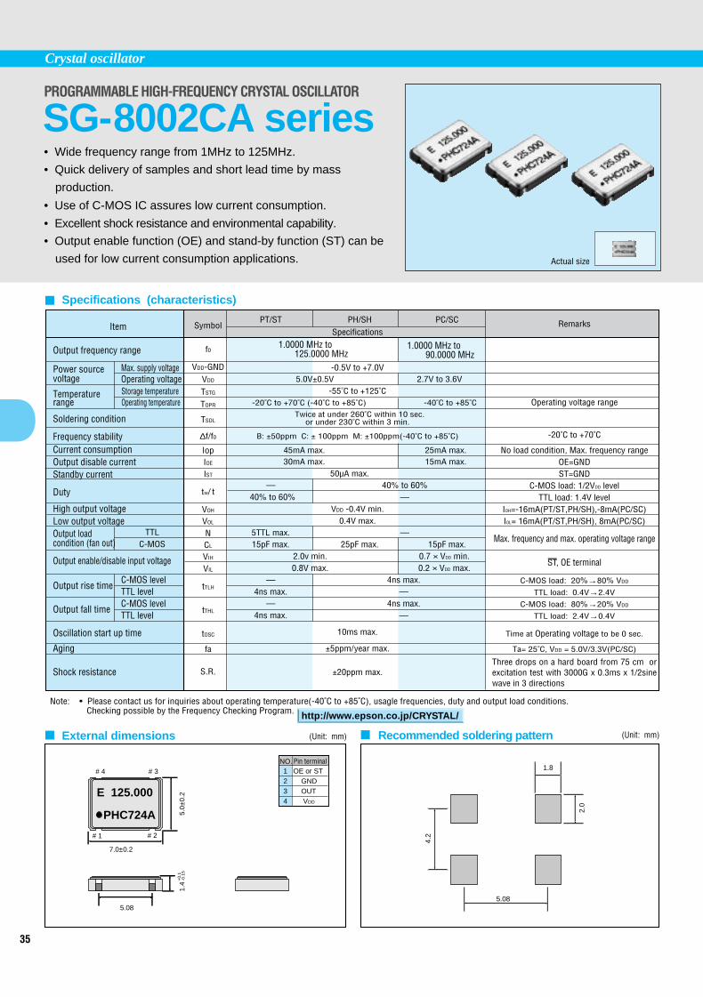
35
Crystal oscillator
Recommended soldering pattern (Unit: mm)
NO.1 OE or ST2 GND3 OUT4 VDD
5.08
1.8
2.0
4.2
7.0±0.2
5.08
5.0±
0.2
# 4 # 3
# 1 # 2
E 125.000
PHC724A
1.4
-0.1
5+
0.1
External dimensions
Specifications (characteristics)
(Unit: mm)
Pin terminal
PROGRAMMABLE HIGH-FREQUENCY CRYSTAL OSCILLATOR
SG-8002CA series
Item
Output frequency range
Power source voltage
Temperature range
Soldering condition
Frequency stabilityCurrent consumptionOutput disable currentStandby current
Duty
High output voltageLow output voltageOutput loadcondition (fan out)
Output enable/disable input voltage
Output rise time
Output fall time
Oscillation start up time
Aging
Shock resistance
Symbol
f0
VDD-GNDVDD
TSTG
TOPR
TSOL
∆f/f0
IopIOE
IST
tw/ t
VOH
VOL
NCL
VIH
VIL
tTLH
tTHL
tOSC
fa
S.R.
TTLC-MOS
C-MOS levelTTL levelC-MOS levelTTL level
PT/ST PH/SH PC/SCSpecifications
-0.5V to +7.0V5.0V±0.5V 2.7V to 3.6V
-55˚C to +125˚C-20˚C to +70˚C (-40˚C to +85˚C) -40˚C to +85˚C
Twice at under 260˚C within 10 sec.or under 230˚C within 3 min.
B: ±50ppm C: ± 100ppm M: ±100ppm(-40˚C to +85˚C)
45mA max. 25mA max.30mA max. 15mA max.
— 40% to 60%40% to 60% —
VDD -0.4V min.0.4V max.
5TTL max. —15pF max. 25pF max. 15pF max.
2.0v min. 0.7 × VDD min.0.8V max. 0.2 × VDD max.
— 4ns max.4ns max. —
— 4ns max.4ns max. —
10ms max.
±5ppm/year max.
±20ppm max.
Remarks
Operating voltage range
-20˚C to +70˚C
No load condition, Max. frequency rangeOE=GNDST=GND
C-MOS load: 1/2VDD levelTTL load: 1.4V level
IOH=-16mA(PT/ST,PH/SH),-8mA(PC/SC)IOL= 16mA(PT/ST,PH/SH), 8mA(PC/SC)
Max. frequency and max. operating voltage range
ST_
, OE terminal
C-MOS load: 20%→80% VDD
TTL load: 0.4V→2.4V
C-MOS load: 80%→20% VDD
TTL load: 2.4V→0.4V
Time at Operating voltage to be 0 sec.
Ta= 25˚C, VDD = 5.0V/3.3V(PC/SC)
Three drops on a hard board from 75 cm orexcitation test with 3000G x 0.3ms x 1/2sinewave in 3 directions
Note: • Please contact us for inquiries about operating temperature(-40˚C to +85˚C), usagle frequencies, duty and output load conditions.Checking possible by the Frequency Checking Program.
Max. supply voltageOperating voltageStorage temperatureOperating temperature
50µA max.
• Wide frequency range from 1MHz to 125MHz.
• Quick delivery of samples and short lead time by mass
production.
• Use of C-MOS IC assures low current consumption.
• Excellent shock resistance and environmental capability.
• Output enable function (OE) and stand-by function (ST) can be
used for low current consumption applications.
1.0000 MHz to 125.0000 MHz
1.0000 MHz to 90.0000 MHz
Actual size
http://www.epson.co.jp/CRYSTAL/

36
Crystal oscillator
Recommended soldering pattern (Unit: mm)
1.3
3.0
5.8
3.0
1.3 3.8
#1 #2
#4 #3
8.65
0.25
9.8
max
.4.
7 m
ax.
4.06
0.25
min
.
No.1234
Pin terminalTS
GNDOUTVDD
External dimensions
Specifications (characteristics)
(Unit: mm)
1.5000MHG2012 AV
5275AE
14.0 max.
5.08 7.620.51
Do not connect TS-pin external device.
HIGH-STABILITY HIGH-FREQUENCY OSCILLATOR
HG-1000/2000 series• Cylindrical AT crystal unit builtin, thus assuring high reliability.
• Excellent shock resistance and heat resistance.
• Low current consumption.
Item
Output frequency range
Power sourcevoltage
TemperaturerangeSoldering condition
Frequency stability
Current consumptionDutyHigh output voltageLow output voltageOutput load conditionOutput rise timeOutput fall time Oscillation start up timeAging
Shock resistance
Symbol
f0
VDD-GNDVDD
TSTG
TOPR
TSOL
∆f/f0
lop
tW/t
VOH
VOL
CL
tTLH
tTHL
tOSC
fa
S.R.
HG-1012JA HG-2012JA
Specifications1.5000 MHz to 28.63636 MHz
-0.5V to +7.0V5.0V ±0.25V
-55˚C to +125˚C-40˚C to + 85˚C
Under 260˚C within 10 sec. x 2 timesAV: ±20ppm, BV: ±25ppm SV: ±15ppm, AV: ±20ppmBX: ±25ppm, CX: ±30ppm BX: ±25ppm
10mA max.40% to 60%
VDD -0.4V min.0.4V max.15pF max.
8ns max.
4ms max.
±5ppm/year max. ±2ppm/year max.
±10ppm max. ±2ppm max.
Remarks
VDD =4.75V to 5.25V
Ta= -20˚C to +70˚CTa= -40˚C to +85˚CNo load condition
1/2 VDD levelIOH= -0.8mAIOL=3.2mA
20%→80% VDD level80%→20% VDD level
Time at 4.75V to be 0 sec.Ta=25˚C
Three drops on a hard wooden board from75 cm or excitation test with 3000G x 0.3msx 1/2sine wave in 3 directions
Max. supply voltageOperating voltageStorage temperatureOperable temperature
Actual size

37
Crystal oscillator
Recommended soldering pattern
Stability / Temperature range Variable frequency range
(Unit: mm)
1.3
3.0
5.8
3.0
1.3 3.8
No.1234
Pin terminalVC
GNDOUTVDD
External dimensions
Specifications (characteristics)
(Unit: mm)
9.8m
ax.
8.65
14.0 max.
4.06
4.7m
ax.
0.25
min0.51
5.08
0.25
7.62
# 4 # 3
# 1 # 2
VG1011 BXK27.0000M
7100AE
± 15ppm± 20ppm± 25ppm
SAB
VNo.
No.
–G, K, N
–
WB––
X––
G, K, N
-20˚C to 70˚C -30˚C to 75˚C -40˚C to 85˚CB
G
K
N
± 20ppm min.
± 50ppm min.
± 75ppm min.
± 100ppm min.
Variable frequency rangeTemperature rangeStability
VOLTAGE-CONTROLLED CRYSTAL OSCILLATOR
VG-1011JA series• High accuracy and high reliability due to trimmerless design.
• Built-in heat-resisting AT-cut crystal provides heat resistance
equivalent to that of general-purpose ICs.
• Use of C-MOS IC assures low current consumption.
• Excellent shock resistance and environmental capability.
• Supply voltage: 5V, Control voltage:5V
Item
Output frequency range
Power sourcevoltage
TemperaturerangeSoldering conditionFrequency stabilityCurrent consumptionVariable frequency rangeInput resistanceFrequency change polarityDuty
Output voltage
Output load condition (fan out)
Output rise time
Output fall time
Oscillation start up timeAging
Shock resistance
Symbol
f0
VDD-GND
VDD
TSTG
TOPR
TSOL
∆f/f0
lop
∆fC
ZIN
tW/t
VOH
VOL
N/CL
tTLH
tTHL
tOSC
fa
S.R.
Specifications
1.5000 MHz to 28.63636 MHz
-0.5V to +7.0V
5.0V ±0.5V
-55˚C to +125˚C
As per below table
Twice at under 260˚C whthin 10 sec.
As per below table
10mA max.
As per below table
10MΩ min.
Positive polarity
40% to 60%
VDD -0.4V min.
0.4V max.2TTL or 15pF max.
8ns. max.5ns. max.8ns. max.
5ns. max.
4ms. max.
±5ppm max.
±5ppm max.
Remarks
No load condition
VC=2.5±2.0V
DC Level
VC=0.5 to 4.5V
1.4V or 1/2VDDlevel
IOH= -0.8mA
IOL=1.6mA
TTL load/C-MOS load
C-MOS load: 20%→80% VDD
TTL load: 0.4V→2.4V
C-MOS load: 80%→20% VDD
TTL load: 2.4V→0.4V
Time at 4.5V to be 0 sec.Ta=25˚C, VDD =5V, first year
Three drops on a hard board from 75 cm orexcitation test with 3000G x 0.3ms x1/2sine wave in 3 directions
Max. supply voltageOperating voltage
Storage temperatureOperating temperature
Actual size
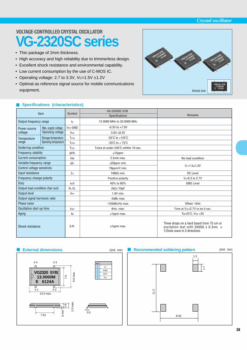
38
Crystal oscillator
Specifications (characteristics)
Recommended soldering pattern (Unit: mm) External dimensions (Unit: mm)
13.0 max.
7.62
9.6
max
.
7.6
1.8
0 m
in. 2.0
max
.
# 4 # 3
# 1 # 2
NO.
1 VC
2 GND
3 OUT
4 VDD
0.5
VG2320 SYB13.0000M
E 6124A
8.92
1.3
1.7
11.2
VOLTAGE-CONTROLLED CRYSTAL OSCILLATOR
VG-2320SC series• Thin package of 2mm thickness.
• High accuracy and high reliability due to trimmerless design.
• Excellent shock resistance and environmental capability.
• Low current consumption by the use of C-MOS IC.
• Operating voltage: 2.7 to 3.3V, VC=1.5V ±1.2V
• Optimal as reference signal source for mobile communications
equipment.
Item
Output frequency range
Power sourcevoltage
Temperaturerange
Soldering conditionFrequency stabilityCurrent consumptionVariable frequency rangeControl voltage sensitivityInput resistanceFrequency change polarityDutyOutput load condition (fan out)Output levelOutput signal harmonic ratioPhase noiseOscillation start up timeAging
Shock resistance
Symbol
f0
VDD-GND
VDD
TSTG
TOPR
TSOL
∆f/f0
lop
∆fC
ZIN
tW/t
RL/CL
VPP
tOSC
fa
S.R.
Specifications
12.0000 MHz to 20.0000 MHz
-0.3V to +7.0V
3.0V ±0.3V
-55˚C to +125˚C
-20˚C to + 75˚C
Twice at under 240˚C whthin 10 sec.
±15ppm
2.5mA max.
±20ppm min.
19ppm/V min.
10MΩ min.
Positive polarity
40% to 60%
2kΩ /10pF
1.0V min.
-5dBc max.
-120dBc/Hz max.
4ms. max.
±1ppm max.
±1ppm max.
Remarks
No load condition
VC=1.5±1.2V
DC Level
VC=0.3 to 2.7V
GND Level
Offset: 1kHz
Time at VDD=2.7V to be 0 sec.
Ta=25˚C, VDD =3V
Three drops on a hard board from 75 cm orexcitation test with 3000G x 0.3ms x1/2sine wave in 3 directions
Max. supply voltageOperating voltage
Storage temperatureOperating temperature
VG-2320SC SYB
Actual size
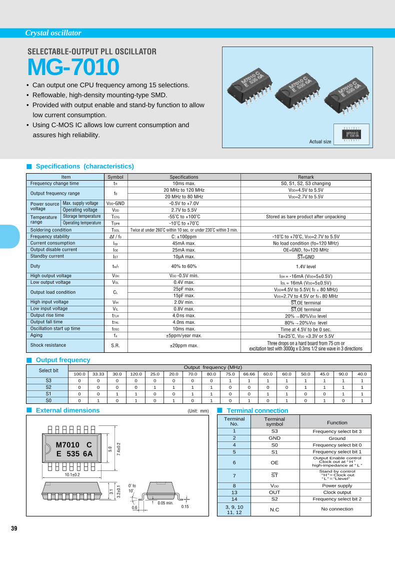
39
Crystal oscillator
Terminal connection External dimensions
Specifications (characteristics)
Output frequency
(Unit: mm)
M7010 C535 6AE 7.
4±0.
23.
2±0.
1
5.0
3.1
10.1±0.2
0.150.60.05 min.
0˚ to 10˚
SELECTABLE-OUTPUT PLL OSCILLATOR
MG-7010• Can output one CPU frequency among 15 selections.
• Reflowable, high-density mounting-type SMD.
• Provided with output enable and stand-by function to allow
low current consumption.
• Using C-MOS IC allows low current consumption and
assures high reliability.
ItemFrequency change time
Output frequency range
Power sourcevoltage
Temperaturerange
Soldering conditionFrequency stabilityCurrent consumptionOutput disable currentStandby current
Duty
High output voltageLow output voltage
Output load condition
High input voltageLow input voltageOutput rise timeOutput fall time Oscillation start up timeAging
Shock resistance
Symboltft
f0
VDD-GNDVDD
TSTG
TOPR
TSOL
∆f / f0
lop
IOE
IST
tw/t
VOH
VOL
CL
VIH
VIL
tTLH
tTHL
tOSC
fa
S.R.
Specifications10ms max.
20 MHz to 120 MHz20 MHz to 80 MHz
-0.5V to +7.0V2.7V to 5.5V
-55˚C to +100˚C-10˚C to +70˚C
Twice at under 260˚C within 10 sec. or under 230˚C within 3 min.C: ±100ppm45mA max.25mA max.10µA max.
40% to 60%
VDD -0.5V min.0.4V max.25pF max.15pF max.2.0V min.0.8V max.4.0ns max.4.0ns max.10ms max.
±5ppm/year max.
±20ppm max.
RemarkS0, S1, S2, S3 changing
VDD=4.5V to 5.5VVDD=2.7V to 5.5V
Stored as bare product after unpacking
-10˚C to +70˚C, VDD=2.7V to 5.5VNo load condition (fo=120 MHz)
OE=GND, fo=120 MHzST_
=GND
1.4V level
IOH = -16mA (VDD=5±0.5V)IOL = 16mA (VDD=5±0.5V)
VDD=4.5V to 5.5V( f0 ≤ 80 MHz)VDD=2.7V to 4.5V or f0 > 80 MHz
ST_
,OE terminalST_
,OE terminal20%→80%VDD level80%→20%VDD level
Time at 4.5V to be 0 sec.Ta=25˚C, VDD =3.3V or 5.5V
Three drops on a hard board from 75 cm orexcitation test with 3000g x 0.3ms 1/2 sine wave in 3 directions
Select bit
S3S2S1S0
Max. supply voltageOperating voltageStorage temperatureOperating temperature
Output frequency (MHz)100.0
0
0
0
0
33.33
0
0
0
1
30.0
0
0
1
0
120.0
0
0
1
1
25.0
0
1
0
0
20.0
0
1
0
1
70.0
0
1
1
0
80.0
0
1
1
1
75.0
1
0
0
0
66.66
1
0
0
1
60.0
1
0
1
0
60.0
1
0
1
1
50.0
1
1
0
0
45.0
1
1
0
1
90.0
1
1
1
0
40.0
1
1
1
1
TerminalNo.
1
2
4
5
6
7
81314
3, 9, 1011, 12
Terminalsymbol
S3
GND
S0
S1
OE
__ST
VDD
OUTS2
N.C
Function
Frequency select bit 3
Ground
Frequency select bit 0
Frequency select bit 1Output Enable control
Clock out at “ H ”high-impedance at “ L ”
Stand by control“H”= Clock out“L” = “Llevel”
Power supply
Clock output
Frequency select bit 2
No connection
Actual size

40
Crystal oscillator
External dimensions
Block diagram
Absolute Max. rating Specifications (characteristics)
Terminal connection
(Unit: mm)
5.3
max
.2.
54 m
in.
0.2
min
.
6.3
0.2590˚ to105˚
7.62
19.8 max.
Operating range
oscillation source frequency is 17.7340 to 40.000 MHz Frequency characteristics
32.0000MHz C
1 2 3 4 5 6 7
14 13 12 11 10 9 8
15.24
MG3020 1120AE
V DD
1/2SEL EXC
FOUT OUT1
Output circuit
OUT2 OUT3 OUT4 OUT5
CSEL
RESET
GND
Synchronous counter
Clock pulse select circuit
Dividing ratio select circuit
1/2 divider
Oscillationcircuit
MULTI-OUTPUT CRYSTAL OSCILLATOR
MG-3020• Simultaneous output. (1/1, 1/2, 1/4, 1/8 and 1/16 output frequency ratio)
• Builtin cylindrical-type AT-cut crystal unit assures high reliability.
• DIP 14-pin plastic package allows automatic mounting.
• External clock select function, dividing circuit reset function and
1/2 divider select function.
Item
Supply voltage
Input voltage
Output current
Storage temperature
Soldering condition
Symbol
VDD
VI
IO
TSTG
TSOL
Rating
-0.5V to +7.0V
-0.5V to VDD +0.5V
30mA max.
-55˚C to +100˚C
Under 260˚C within 10 sec. (lead part)
Package should be less than 150˚C
Item
Operating voltage
Output current
Operating temperature
Output load condition
Symbol
VDD
IO
TOPR
CL
Rating
Min.
4.5
-10
Typ.
5.0
25
Max.
5.5
1.6
70
15
Unit
V
mA
˚C
pF
Item
Frequency stability
Aging
Symbol
∆f/f0
fa
Specification
±100 ppm
±5 ppm/Y
Remarks
-10 to +70˚C
Ta=25˚C, VDD =5V first year
TerminalVDD
GNDOUT1
OUT2
OUT3
OUT4
OUT5
FOUT
CSEL____
EXC
RESET_____
1/2 SEL______
NC
Pin No.1478910111213
4
5
3
6
1 and 2
Function+5V power supply
GND1/1 source frequency1/2 source frequency1/4 source frequency1/8 source frequency1/16 source frequency
Source frequency
When this pin is made L, the external clock is selected(pull-up resistor incorporated)
External clock pulse input pin
Stops output at RESET_____
=L(pull-up resistor incorporated)
1/2 frequency output at 1/2SEL_____
=L(pull-up resistor incorporated)
NC is not connected internally
When the power switch is turned on in RESET_____
L level mode, please note that all outputbecomes high impedance. To resume normal operation, disable the RESET
_____terminal.
Actual size

41
Crystal oscillator
Specifications (characteristics)
Electric characteristics
RESET timing
External dimensions
Block diagram
Divider IC (without quartz crystal)
4 3 2 7 6
1014
11
1312
5
9
4 3 2 7 6
10141312
5
9
(Unit: mm)
0.25
6.65
4.5
max
.3.
0 m
in.
0.1
min
.
90˚ to105˚
7.62
EXC. CSEL. RESET CLOCK ENABLE RESET
FOUT
8640N8650D( )
CTL1 to 3 CTL1 to 3 CTL4 to 6CTL4 to 6
TEST TEST
OUT OUT
20.5 max.
17.78
80%VDD
50%
Output waveform
RESETDuty=B/A 100
RESET timingtRW
20%VDD
tTHL BA
VSS
VOLVOH
1/2VDD
tTLH tR t E tw
VDD
CSEL
1/1 to 1/107
ProgramDivider
1/1 to 1/107
SPG-8650O only
1/1 to 1/12ProgramDivider
(1/1 to 1/2) 1/1 to 1/12ProgramDividerProgram
Divider
x
OSC.
Pull-up and pull-down resistance 400 K (typ.)
%
S P GEPSON 0103B
8650 B
SELECTABLE-OUTPUT CRYSTAL OSCILLATOR
SPG series• Capable of selecting 57 varieties of frequency output.
• Low current consumption.
• Easy to mount DIP 16-pin package.
Symbol
foVDD-GND
VDD
TSTG
TOPR
TSOL
∆f/f0
falop
ItemModel nameOscillation source frequencyPower sourcevoltage
Temperature rangeSoldering condition (lead part)Frequency toleranceFrequency temperature characteristicsFrequency voltage characteristicsAgingCurrent consumption
Max. supply voltageOperating voltageStorage temperatureOperating temperature
Item
L. input voltage
H. input voltage
L. input current (Reset)
H input current (Reset)
L. input current(input terminal except for Reset)
H input current(input terminal except for Reset)
L. output voltage
H. output voltage
L. output current
H. output current
Output rise time
Output fall time
Duty
Min. reset pulse width
Reset delay time
Reset release synchronous errorExternal signal input frequency
External signal input pulse widthOscillation start up time
Specifications
8640AN 8640BN 8640CN 8650A 8650B 8650C 8650D 8650E 8651A 8651B 8651E600kHz 1MHz 768kHz 60kHz 100kHz 96kHz 153.6kHz 32.768kHz 60kHz 100kHz 32.768kHz
-0.3V to +7.0V5.0V±0.5V
-30˚C to +80˚C-10˚C to +60˚C
-55˚C to +125˚C-10˚C to +70˚C
Under 260˚C within 10 sec.±100ppm ±50ppm ±5ppm ∗ 1
+10/-120ppm±20ppm ±10ppm ±20ppm
1.0mA max. 2.0mA max. 1.5mA max.
±10ppm ±5ppm±3ppm/year max.±5ppm/year max.
0.5mA max.
Remarks
For output frequency, refer to the table in the next page
Package should be less than 150˚CVDD=5V, Ta=25˚C
VDD=5VVDD=4.5 to 5.5V
VDD=5V, Ta=25˚C, first yearNo load condition
∗ 1 Frequency tolerance of 8651 system shows the value guaranteed at the time of shipment.
ItemModel nameInput clock frequencyCurrent consumption
Symbol
lop
Specifications8650 O
1 MHz max.About 2 mA
Remarks
No load condition
SymbolVIL
VIH
IRL
IRH
IIL
IIH
VOL
VOH
IOL
IOH
tTLH
tTHL
tRW
tR
tE
FIN
tIN
tOSC
Min.0
VDD-1.0-30
-0.5
5
VDD-1.01.6
40
1.0
tW-∗ 11/2 to
0.5
Typ.
30
25
0.2
Max.0.8VDD
-50.5
30
0.4
-40605060
1.0tW
1M
1
∗ 2
Unit
V
µA
V
mAµA
ns
%
µs
Hzµss
∗ 1 to=oscillation source cycle. ∗ 2 tw=1/2 cycle of preset frequency. ∗ 3 For more than 1ms until VDD=0→4.5V. Time at 4.5V is to be 0.
Remarks
Reset=GNDReset=VDD
IOL=1.6mA
IOH= -40µAVOL=0.4V
VOH=VDD-1.0V
Except in the case of 1/3 and 1/5
8640N only
∗ 3
VDD=5V±0.5V, Ta=-10 to 70˚C CL ≤ 15pF
Actual size

42
Crystal oscillator
No.12345678
Pin terminalNC
CTL 3CTL 2CTL 1CTL 6CTL 5CTL 4GND
No.161514131211109
Pin terminalVDD
NCRESET
NC (CSEL)NC (EXC)
FOUTTESTOUT
1 2 3 4 5 6 7 8
16 15 14 13 12 11 10 9
NC: Do not connect to the external teminal.For 8650 O
( ) shown 8640N only
11. NC 12. CLOCK 13. ENABLE
Explanation of terminal
8640AN
Terminal connection
8650E 8651E
8650B 8651B
8650A 8651A
8640BN 8650D
8650C
8640CN
Explanation of terminal (8650 O)
CTL3CTL6
CTL3CTL6
(Unit: Hz)
( )8650D0= “L” 1=“H”
CTL3CTL6
CTL3CTL6
CTL3CTL6
Setting of divider output
Baud rate generator
Setting of output frequency
(a) CTL 1 to 6 :(b) OUT :
(c) FOUT :
(d) RESET :
(e) TEST :
(f) EXC (8640N only) :
(g) CSEL (8640N only) :
Programs dividing ratio. (pull-down resistor incorporated.)Output frequency preset by CTL1 to 6. (refer to the procedure forsetting output frequency.)Constantly outputs the oscillation source frequency of builtincrystal unit.Stops output at RESET= “L”.(pull-up resistor incorporated.)Used for the input terminal for testing. When CTL4 is H,output will be 1000 times larger than the preset value atTEST= “H”. (pull-down resistor incorporated.)Serves as input terminal when using an external clock bychanging to the builtin oscillator.Effective only when CSEL is H.When this terminal is made H, the external clock is selected.(pull-down resistor incorporated.)
Treatment of empty terminals. When RESET terminal is not used, this should be connected to VDD,and when TEST terminal, CSEL terminal, and CTL 1 to 6 terminals are not used, to GND.
(Note)
(a) CLOCK: Clock input (max. 1 MHz) (b) ENABLE: Be sure to connect to VDD
CTL100001111
CTL200110011
CTL301010101
Dividing ratio
1/1
1/10
1/2
1/3
1/4
1/5
1/6
1/12
CTL400001111
CTL500110011
CTL601010101
Dividing ratio
1/1 (1/1)
1/10 (1/2)
1/102 (1/2)2
1/103 (1/2)3
1/104 (1/2)4
1/105 (1/2)5
1/106 (1/2)6
1/107 (1/2)7
Set terminal
CTL100001111
CTL200110011
CTL4CTL5
01010101
000
600K60K
300K200K150K120K100K50K
001
60K6K
30K20K15K12K10K5K
0106K
6003K2K
1.5K1.2K
1K500
011
60060
30020015012010050
100606
30201512105
101
6.00.63.02.01.51.21.00.5
110
0.60.060.30.20.150.120.10.05
111
0.060.0060.030.020.0150.0120.010.005
Set terminal
CTL100001111
CTL200110011
CTL4CTL5
01010101
000
1M100K500K
333.3K250K200K
166.6K83.3K
001
100K10K50K
33.3K25K20K
16.6K8.3K
01010K1K5K
3.3K2.5K
2K1.6K
833.3
011
1K100500
333.3250200
166.683.3
100
1001050
33.32520
16.68.3
101
1015
3.332.52
1.60.83
1101
1/101/21/31/41/51/61/12
111
1/101/1001/201/301/401/501/60
1/120
Set terminal
CTL100001111
CTL200110011
01010101
CTL4CTL5
000
60K6K
30K20K15K12K10K5K
001
6.0K600
3.0K2.0K1.5K1.2K1.0K500
010
60060
300200150120100
50
011
606
3020151210
5
100
6.00.63.02.01.51.21.00.5
101
0.6 0.060.30.20.150.120.10.05
110
0.060.0060.030.020.0150.0120.010.005
111
0.0060.00060.0030.0020.00150.00120.0010.0005
Set terminal
CTL100001111
CTL200110011
CTL4CTL5
01010101
000
100K10K50K
33.3K25K20K
16.6K8.3K
00110K1K5K
3.3K2.5K
2K1.6K
833.3
010
1K100500
333.3250200
166.683.3
011
1001050
33.32520
16.68.3
1001015
3.332.52
1.60.83
1011
1/101/21/31/41/51/61/12
110
1/101/1001/201/301/401/501/601/120
111
1/1001/10001/2001/3001/4001/5001/6001/1200
Set terminal
CTL100001111
CTL200110011
CTL4CTL5
01010101
000
327683276.816384
10922.68192
6553.65461.32730.6
001
3276.8327.681638.4
1092.26819.2
655.36546.13273.06
010
327.6832.768163.84
109.22681.92
65.53654.61327.306
011
32.7683.276
16.38410.9228.1926.5535.4612.730
100
3.2760.3271.6381.0920.8190.6550.5460.273
101
0.32760.03270.16380.10920.08190.06550.05460.0273
110
0.032760.003270.016380.010920.008190.006550.005460.00273
111
0.003270.000320.001630.001090.000810.000650.000540.00027
CTL1
0
1
0
0
1
CTL2
0
0
0
1
0
CTL3
0
1
1
0
0
CTL4
0
0
0
0
0
CTL5
0
0
0
0
0
CTL6
0
0
0
1
1
Output frequency768 kHz
153.6
76.8
38.4
19.2
Baud rate outputexample (fo/16)
48000bits/sec.
9600
4800
2400
1200
CTL1
0
1
0
0
0
1
1
1
CTL2
0
0
0
1
1
0
1
1
CTL3
0
1
1
0
1
0
0
1
CTL4
0
0
0
0
0
0
0
0
CTL5
0
0
0
0
0
0
0
0
CTL6
0
0
0
1
1
1
1
1
Output frequency96.0 kHz
19.2
9.6
4.8
3.2
2.4
1.6
0.8
Baud rate outputexample (to/16)
6000bits/sec.120060030020015010050
CTL1
0
0
0
0
0
0
0
0
1
0
1
CTL200000010101
CTL300000010001
CTL400001111111
CTL500110001010
CTL601010100010
Output frequency153.6 kHz
76.838.419.2
9.64.83.22.41.61.20.8
Baud rate outputexample (fo/16)
9600bits/sec.480024001200
600300200150100
7550
Note: Lower digits are omitted.
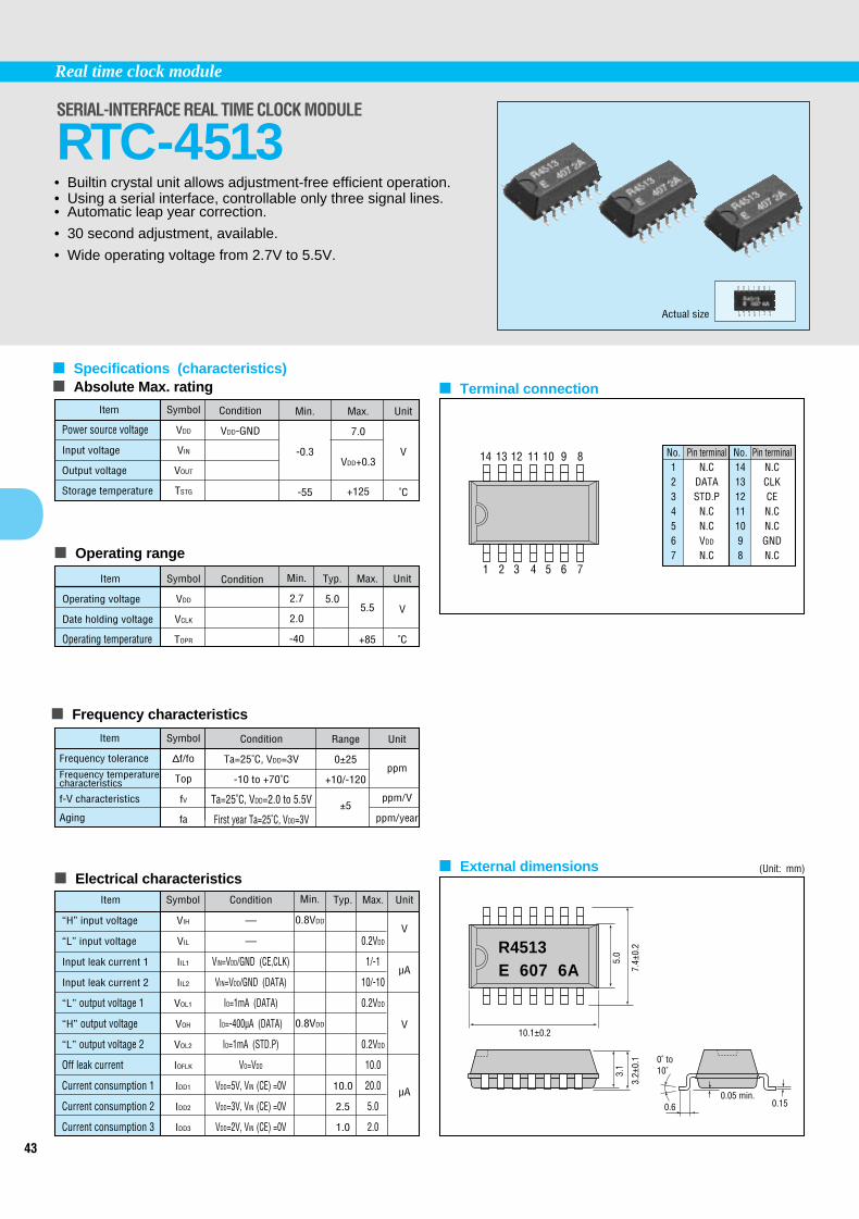
43
Real time clock module
Absolute Max. rating Specifications (characteristics)
Operating range
Frequency characteristics
Electrical characteristics External dimensions (Unit: mm)
R4513607 6AE 7.
4±0.
23.
2±0.
1
5.0
3.1
10.1±0.2
Terminal connection
0.150.60.05 min.
No.1234567
Pin terminalN.C
DATASTD.P
N.CN.CVDD
N.C
No.141312111098
Pin terminalN.CCLKCEN.CN.CGNDN.C
1 2 3 4 5 6 7
14 13 12 11 10 9 8
0˚ to 10˚
• Builtin crystal unit allows adjustment-free efficient operation.• Using a serial interface, controllable only three signal lines.• Automatic leap year correction.
• 30 second adjustment, available.
• Wide operating voltage from 2.7V to 5.5V.
SERIAL-INTERFACE REAL TIME CLOCK MODULE
RTC-4513
Item
Power source voltage
Input voltage
Output voltage
Storage temperature
Symbol
VDD
VIN
VOUT
TSTG
Condition
VDD-GND
Min.
-0.3
-55
Max.
7.0
VDD+0.3
+125
Unit
V
˚C
Item
Operating voltage
Date holding voltage
Operating temperature
Symbol
VDD
VCLK
TOPR
Condition Min.
2.7
2.0
-40
Typ.
5.0
Max.
5.5
+85
Unit
V
˚C
Item
Frequency tolerance
Frequency temperaturecharacteristics
f-V characteristics
Aging
Symbol
∆f/fo
Top
fV
fa
Condition
Ta=25˚C, VDD=3V
-10 to +70˚C
Ta=25˚C, VDD=2.0 to 5.5V
First year Ta=25˚C, VDD=3V
Range
0±25
+10/-120
±5
Unit
ppm
ppm/V
ppm/year
Item
“H” input voltage
“L” input voltage
Input leak current 1
Input leak current 2
“L” output voltage 1
“H” output voltage
“L” output voltage 2
Off leak current
Current consumption 1
Current consumption 2
Current consumption 3
Symbol
VIH
VIL
IIL1
IIL2
VOL1
VOH
VOL2
IOFLK
IDD1
IDD2
IDD3
Condition
—
—
VIN=VDD/GND (CE,CLK)
VIN=VDD/GND (DATA)
IO=1mA (DATA)
IO=-400µA (DATA)
IO=1mA (STD.P)
VO=VDD
VDD=5V, VIN (CE) =0V
VDD=3V, VIN (CE) =0V
VDD=2V, VIN (CE) =0V
Min.
0.8VDD
0.8VDD
Typ.
10.0
2.5
1.0
Max.
0.2VDD
1/-1
10/-10
0.2VDD
0.2VDD
10.0
20.0
5.0
2.0
Unit
V
µA
V
µA
Actual size

44
Real time clock module
Switching characteristics
Block diagram
Register table
Timing chart
Write mode
Read mode
t CKS
tDS
tRF tRD tRF
tRZ
Hi-z
tDH
t CSt CH t CKH
t CR
t WL t WH
CLK
CLK
CLK
DATA
DATA
CE
CE
STD.P
VDD
GND
DATA
CLK
CE
OSC
Decoder
Address counterData buffer
Clock& calender
Control registerCD,CE,CF
Address
0
1
2
3
4
5
6
7
8
9
A
B
C
D
E
F
A3
0
0
0
0
0
0
0
0
1
1
1
1
1
1
1
1
A2
0
0
0
0
1
1
1
1
0
0
0
0
1
1
1
1
A1
0
0
1
1
0
0
1
1
0
0
1
1
0
0
1
1
A0
0
1
0
1
0
1
0
1
0
1
0
1
0
1
0
1
Registersymbol
S1
S10
MI1
MI10
H1
H10
D1
D10
MO1
MO10
Y1
Y10
W
CD
CE
CF
D3
(MSB)
s8
f0
mi8
fr
h8
fr
d8
fr
mo8
fr
y8
y80
fr
30ADJ
t1
TEST
D2
s4
s40
mi3
mi40
h4
pm/am
d4
∗
mo4
y4
y40
w4
IRQ-F
t0
24/12
D1
s2
s20
mi2
mi20
h2
h20
d2
d20
mo2
y2
y20
w2
CAL/HW
INT/STND
STOP
D0
(LSB)
s1
s10
mi1
mi10
h1
h10
d1
d10
mo1
mo10
y1
y10
w1
HOLD
MASK
RESET
0 to 9
0 to 5
0 to 9
0 to 5
0 to 9
0 to 1,2
0 to 9
0 to 3
0 to 9
0 to 1
0 to 9
0 to 6
—
Register name
1-second digit register
10-second digit register
1-minute digit register
10-minute digit register
1-hour digit register
10-hour digit register
1-day digit register
10-day digit register
1-month digit register
10-month digit register
1-year digit register
10-year digit register
day of the week register
Control register D
Control register E
Control register F
Item
CLK “H” time
CLK “L” time
CE setup time
CE hold time
CE recovery time
CLK setup time
CLK hold time
Write data setup time
Write data hold time
Read data delay time
Read data disable delay time
CLK rise time/fall time
Symbol
tWH
tWL
tCS
tCH
tCR
tCKS
tCKH
tDS
tDH
tRD
tRZ
tRF
Condition
—
CL=50pF
—
Min.
300
150
200
300
20
50
—
Max.
—
250
100
20
Unit
ns
∗

45
Real time clock module
Absolute Max. rating Specifications (characteristics)
Operating range
Frequency characteristics
DC characteristics
External dimensions (Unit: mm)
R4543 B
607 6AE 7.4±
0.2
3.2±
0.1
5.0
3.1
10.1±0.2
Terminal connection
0.150.60.05 min.
No.123456789101112131415161718
4543SAGNDN.CCEFSEL
WRFOE
N.CN.CVDD
CLKDATAN.CN.CFOUT
—
—
—
—
4543SBN.CN.CN.CN.CFOE
WRFSEL
CEGNDFOUT
DATACKLN.CVDD
N.CN.CN.CN.C
1 2 3 4 5 6 7
14 13 12 11 10 9 8
1 2 3 4 5 6
18 17 16 15 14 13
7
12
8
11
9
10
0˚ to 10˚
R4543 B
607 6AE 7.8±
0.2
2.0
max
.
5.4
1.8
11.4±0.2
0.150.60.05 min.
0˚ to 10˚
RTC-4543SA
RTC-4543SA (SOP 14-pin)
RTC-4543SB
RTC-4543SB (SOP 18-pin)
• Builtin crystal unit allows adjustment-free efficient operation.
• Automatic leap year correction.
• Output selectable between 32.768 KHz/1 Hz.
• Operating voltage range: 2.5V to 5.5V.
• Supply voltage detection voltage: 1.7±0.3V.
• Low current consumption: 1.0 µA/2.0V (Max.)
SERIAL-INTERFACE REAL TIME CLOCK MODULE
RTC-4543
Item
Power source voltage
Input voltage
Output voltage
Storage temperature
Symbol
VDD
VIN
VOUT
TSTG
Condition
VDD-GND
—
Min.
-0.3
-55
Max.
7.0
VDD+0.3
+125
Unit
V
˚C
Item
Operating voltage
Date holding voltage
Operating temperature
Symbol
VDD
VCLK
TOPR
Condition
—
Min.
2.5
1.4
-40
Max.
5.5
+85
Unit
V
˚C
Item
Frequency tolerance
Frequency temperaturecharacteristics
Frequency voltagecharacteristics
Oscillation start time
Aging
Symbol
∆f/fo
Top
fV
tOSC
fa
Condition
Ta=25˚C, VDD=5V
-10 to +70˚C
Ta=25˚C, VDD=2.0 to 5.5V
Ta=25˚C, VDD=2.5V
First year Ta=25˚C, VDD=5V
Range
5±23
+10/-120
±2
3
±5
Unit
ppm
ppm/V
s
ppm/year
Item
“H” input voltage“L” input voltageInput off-leak current
“H” output voltage
“L” output voltage
Output leak current
Supply detection voltage
Output load conditions
Currentconsumption
Symbol
VIH
VIL
IOFF
VOH1
VOH2
VOL1
VOL2
IOZH
IOZL
VDT
CL
NIDD1
IDD2
IDD3
IDD4
IDD5
IDD6
123456
Condition Min. Typ. Max. Unit
VDD=5.0VVDD=3.0VVDD=5.0VVDD=3.0VVOUT=5.5VVOUT=0V
IOH=-1.0 mADATA, FOUT pins
CE="L", FOE="L"FSEL="H"
CE="L", FOE="H"FSEL="L"
No load on the FOUT pin
DATA, FOUT pins
FOUT pin30 pF(max.)
2LS-TTL
—
—
—
1.7
VDD=5.0VVDD=3.0VVDD=2.0VVDD=5.0VVDD=3.0VVDD=2.0V
1.51.00.54.02.51.5
3.02.01.0
10.06.54.0
WR, DATA, CE, CLK, FOE,FSEL pins
WR, CE, CLK, FOE,FSEL pins
0.8VDD
—
4.52.5
—
-1.0
1.4
—0.2VDD
0.5
—
0.50.8
1.0
2.0
V
µA
µA
µA
V
V
(VDD=5V±0.5V, Ta=-40 to 85˚C)
Actual size
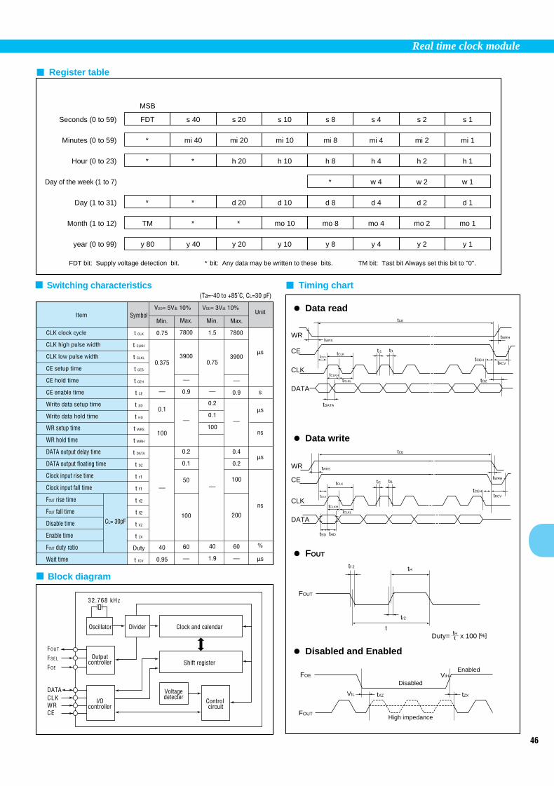
46
Real time clock module
FDT
MSB
Seconds (0 to 59) s 40 s 20 s 10 s 8 s 4 s 2 s 1
∗Minutes (0 to 59) mi 40 mi 20 mi 10 mi 8 mi 4 mi 2 mi 1
∗Hour (0 to 23) ∗ h 20 h 10 h 8 h 4 h 2 h 1
Day of the week (1 to 7) ∗ w 4 w 2 w 1
∗Day (1 to 31) ∗ d 20 d 10 d 8 d 4 d 2 d 1
TMMonth (1 to 12) ∗ ∗ mo 10 mo 8 mo 4 mo 2 mo 1
y 80year (0 to 99) y 40 y 20 y 10 y 8 y 4 y 2 y 1
FDT bit: Supply voltage detection bit. ∗ bit: Any data may be written to these bits. TM bit: Tast bit Always set this bit to "0".
Switching characteristics
Block diagram
Register table
Timing chart
32.768 kHz
FOUT
CLKWRCE
FSEL
FOE
DATA
(Ta=-40 to +85˚C, CL=30 pF)
Outputcontroller
I/Ocontroller
Control circuit
Voltagedetecter
DividerOscillator Clock and calendar
Shift register
FOE
FOUT
FOUT
DATA
CLK
CE
WR
DATA
CLK
CE
WR
VIL
VIHEnabled
High impedance
Disabled
tXZ
tf 2
tSD tHD
tDATA
tCLKH
tCLKH
tCES
tCES
tCLK
tCLK
tWRS
tWRS
tr1
tCE
tCE
tf1
tr1 tf1
tCEH
tOZ
tCEH
tRCV
tRCV
tWRH
tWRH
tCLKL
tCLKL
tr2
t
tH
tZX
Duty= x 100 ttH [%]
Data read
Data write
FOUT
Disabled and Enabled
Item
CLK clock cycle
CLK high pulse width
CLK low pulse width
CE setup time
CE hold time
CE enable time
Write data setup time
Write data hold time
WR setup time
WR hold time
DATA output delay time
DATA output floating time
Clock input rise time
Clock input fall time
FOUT rise time
FOUT fall time
Disable time
Enable time
FOUT duty ratio
Wait time
Symbol
t CLK
t CLKH
t CLKL
t CES
t CEH
t CE
t SD
t HD
t WRS
t WRH
t DATA
t DZ
t r1
t f1
t r2
t f2
t XZ
t ZX
Duty
t rcv
Min.
0.75
0.375
—
0.1
100
—
40
0.95
Max.
7800
3900
—
0.9
—
0.2
0.1
50
100
60
—
Min.
1.5
0.75
—
0.2
0.1
100
—
40
1.9
Max.
7800
3900
—
0.9
—
0.4
0.2
100
200
60
—
Unit
µs
s
µs
ns
µs
ns
%
µs
CL= 30pF
VDD= 5V± 10% VDD= 3V± 10%

47
Real time clock module
Absolute Max. rating Specifications (characteristics)
Operating range
Frequency characteristics
DC characteristics
External dimensions (Unit: mm)
R4553 A
6496E 7.4±
0.2
3.2±
0.1
5.0
3.1
10.1±0.2
Terminal connection
0.150.60.05 min.
No.1234567
Pin terminalGNDWRSIN
SCKL1L2L3
No.141312111098
Pin terminalTPOUT
SOUT
CS1
CS0
L5L4VDD
1 2 3 4 5 6 7
14 13 12 11 10 9 8
VDD=5V±10% (GND=OV, Ta=-30˚C to +70˚C) VDD=3V±10% (GND=OV, Ta=-30˚C to +70˚C)
L1 to L5 are test pin. Do not connect them to any terminals.
SERIAL-INTERFACE REAL TIME CLOCK MODULE
RTC-4553
Item
Supply voltage
Input voltage
Output voltage
Storage temperature
Soldering conditions
Symbol
VDD
VIN
VOUT
TSTG
TSOL
Condition
VDD-GND
SIN,SCK__
, W__
R, CS__
0, CS1
SOUT, TPOUT____
Stored without tape & reel
Min.
-0.3
-55
Max.
+6.0
VDD+0.3
+125
Unit
V
˚C
Twice at under 260˚C within 10 sec. or under 230˚C within 3 min.
Item
Operating voltage
Operating temperature
Symbol
VDD
TOPR
Condition
—
Min.
2.7
-30
Typ.
5.0
—
Max.
5.5
+70
Unit
V
˚C
Item
Frequency tolerance
Frequency temperature characteristicsFrequency voltage characteristics
Aging
Symbol
∆f/fo
Top
fv
fa
Condition
Ta=25˚C,VDD=5V
AA
A
B
Ta=-10 to 70˚C, VDD=5VReference at 25˚CTa=Fix, VDD=2 to 5.5VReference at 5V
Ta=25˚C, VDD=5V, first year
Range
5±5
5±10
5±20
+10-120
±5
Unit
ppm
ppm/year
Item
Data holding voltage
Current consumption
Output voltage
Off leak current
Input voltage
Input current
Oscillation start-up time
Item
Data holding voltage
Current consumption
Output voltage
Off leak current
Input voltage
Input current
Oscillation start-up time
Symbol
VDH
IDD1
IDD2
VOH
VOL
IOZH
IOZL
VIH
VIL
IIH
IIL
Tosc
Condition
—
SCK___
=500 kHz
SCK___
=DC
IOH=-400µA
IOL=1.6mA
VOUT=5.5V
VOUT=0V
—
VIN=5.5V
VIN=0V
Ta=25˚C
Min.
2.0
—
VDD-0.4
—
-2.0
4/5 VDD
—
-2.0
—
Typ.
—
1.0
—
Max.
5.5
100
3.0
—
0.4
2.0
—
1/5 VDD
2.0
3.0
Unit
V
µA
V
µA
V
µA
s
Unit
V
µA
V
µA
V
µA
s
Symbol
VDH
IDD1
IDD2
VOH
VOL
IOZH
IOZL
VIH
VIL
IIH
IIL
Tosc
Condition
—
SCK___
=300 kHz
SCK___
=DC
IOH=-400µA
IOL=1.6mA
VOUT=3.3V
VOUT=0V
—
VIN=3.3V
VIN=0V
Ta=25˚C
Min.
2.0
—
VDD-0.4
—
-2.0
4/5 VDD
—
-2.0
—
Typ.
—
1.0
—
Max.
3.3
100
3.0
—
0.4
2.0
—
1/5 VDD
2.0
3.0
• Builtin crystal unit allows adjustment-free efficient operation.• The small package makes high-density mounting possible. (SOP 14-pin)• Automatic calendar function (year, month, day, day of the week, hour, minute,
second).• Automatic leap year correction. (up to 2099)• Builtin 30 x 4-bit S-RAM.• High-speed access.• Reference pulse output. (1024 Hz, 1/10 Hz)• Low current consumption. (1 µA typical)• Similar mounting method to that used for universal type SMD IC.
Actual size

48
Real time clock module
Switching characteristics
Block diagram
Register table
Timing chart
32.768 kHz
TPOUT
SOUT
SCKSIN
CS1
CS0
WR
(Ta=-30˚C to +70˚C, VDD=5V±10%, GND=OV)
Note: ∗ TEST bit should be “0”.
CS0
SCK
SIN
WR
SOUT
SOUT
CS1
TPOUT
SCK
CS0
t WCKL
t SD
t SWR
t DSZ1
t DSO
t DPZ1 t DPZ2
t DSZ2
t PS
t HWR
t HD
t WCKH t HCS
1/f CLK
10%90%
90%
90%
10%
10%
90%
90%
90%
90%
10%
10%
10%
10%90%
10%
10%
tSCS
SCKOSC Counter
Outputcontrol RAM
(120bit)
Inputcontrol
Output control
Shift register
Control circuit
Controlregister
1
Controlregister
2
Controlregister
3
Sec. Min. Hou.Dayof
WeekDay Mon. Year
Address
0
1
2
3
4
5
6
7
8
9
A
B
C
D
E
F
A3
0
0
0
0
0
0
0
0
1
1
1
1
1
1
1
1
A2
0
0
0
0
1
1
1
1
0
0
0
0
1
1
1
1
A1
0
0
1
1
0
0
1
1
0
0
1
1
0
0
1
1
A0
0
1
0
1
0
1
0
1
0
1
0
1
0
1
0
1
MODE 0Counter control register
Registersymbol
S1
S10
MI1
MI10
H1
H10
W
D1
D10
MO1
MO10
Y1
Y10
C1
C2
C3
D3
S8
0
mi8
0
h8
PM/AM
0
d8
0
mo8
0
y8
y80
TPS
BUSY
SYSR
D2
S4
S40
mi4
mi40
h4
0
w4
d4
0
mo4
0
y4
y40
30ADJ
PONC
TEST
D1
S2
S20
mi2
mi20
h2
h20
w2
d2
d20
mo2
0
y2
y20
CNTR
—
MS1
D0
S1
S10
mi1
mi10
h1
h10
w1
d1
d10
mo1
mo10
y1
y10
24/12
∗
MS0
Register name
1-second digit register
10-second digit register
1-minute digit register
10-minute digit register
1-hour digit register
10-hour digit register
Day of the week digit register
1-day digit register
10-day digit register
1-month digit register
10-month digit register
1-year digit register
10-year digit register
Control register 1
Control register 2
Control register 3
MODE 1
User RAM Domain 1
D3
RA3
RA7
RA11
RA15
RA19
RA23
RA27
RA31
RA35
RA39
RA43
RA47
RA51
RA55
RA59
D2
RA2
RA6
RA10
RA14
RA18
RA22
RA26
RA30
RA34
RA38
RA42
RA46
RA50
RA54
RA58
D1
RA1
RA5
RA9
RA13
RA17
RA21
RA25
RA29
RA33
RA37
RA41
RA45
RA49
RA53
RA57
D0
RA0
RA4
RA8
RA12
RA16
RA20
RA24
RA28
RA32
RA36
RA40
RA44
RA48
RA52
RA56
MODE 2
User RAM Domain 2
D3
RA63
RA67
RA71
RA75
RA79
RA83
RA87
RA91
RA95
RA99
RA103
RA107
RA111
RA115
RA119
D2
RA62
RA66
RA70
RA74
RA78
RA82
RA86
RA90
RA94
RA98
RA102
RA106
RA110
RA114
RA118
D1
RA61
RA65
RA69
RA73
RA77
RA81
RA85
RA89
RA93
RA97
RA101
RA105
RA109
RA113
RA117
D0
RA60
RA64
RA68
RA72
RA76
RA80
RA84
RA88
RA92
RA96
RA100
RA104
RA108
RA112
RA116
Same as MODE 0 Same as MODE 0
Item
SCK___
input frequency
SCK___
“L” time
SCK___
“H” time
SCK___
pause time
CS0
__setup time
CS0
__hold time
SIN data setup time
SIN data Hold time
WR___
setup time
WR___
hold time
SOUT delay time
CS0
__, and CS1 enable to SOUT output
CS0
__disenable to SOUT high Z
CS1 enable to SOUT output
CS1 enable to SOUT high Z
Symbol
fSCK
tWSCKL
tWSCKH
tPS
tSCS
tHCS
tSD
tHD
tSWR
tHWR
tDSO
tDSZ1
tDSZ2
tDPZ1
tDPZ2
Condition
—
—
CL=100pF
Min.
—
1.0
0
0.5
0.2
1.0
0.5
—
Typ.
—
—
150
—
Max.
500
—
—
500
100
Unit
kHz
µs
ns

49
Real time clock module
The I C-Bus is a trademark of Philips Electronics N.V.2
Absolute Max. rating Specifications (characteristics)
Operating range
Frequency characteristics
DC characteristics
External dimensions (Unit: mm)
Terminal connection
No.123456789101112131415161718
8583GND1SCL
GND2SDAN.CN.CA0
OSC1N.CN.CVDD
N.CN.CINT
8593N.CSCLSDAN.CGNDOSC1N.CN.C
RESETN.CVDD
N.CN.CINT
8593SBN.CN.CN.CN.CN.CN.CN.C
RESETGNDSDASCLINTVDD
OSC1N.CN.CN.CN.C
1 2 3 4 5 6 7
14 13 12 11 10 9 8
1 2 3 4 5 6
18 17 16 15 14 13
7
12
8
11
9
10
RTC-8583/8593(SA)
RTC-8593SB
R8593 B
607 6AE 7.4±
0.2
3.2±
0.1
5.0
3.1
10.1±0.2
0.150.60.05 min.
0˚ to 10˚
R8593 B
607 6AE 7.8±
0.2
2.0
max
.
5.4
1.8
11.4±0.2
0.150.60.05 min.
0˚ to 10˚
RTC-8583/8593(SA)
RTC-8593SB
(SOP 14-pin)
(SOP 18-pin)
I C-BUS COMPATIBLE REAL TIME CLOCK MODULE
RTC-8583/8593• Builtin crystal unit. Adjustment free with 10pF external capacitor.• Small package (SOP 14-pin).• Three mode operations: internal crystal oscillation, external 50 Hz
clock and event counter.• I
2
C-Bus inter face compatible.• Builtin 240 x 8 bit S-RAM available (RTC8583).• Alarm and timer functions available.• Wide operating voltage range 2.5V to 6.0V.• Wide data hold voltage range 1.0V to 6.0V.• Low current consumption (RTC8593, 1.0µA typical).
Item
Supply voltage
Input voltage
Input current
Output current
Storage temperature
Symbol
VDD
VIN
Ii
Io
TSTG
Condition
VDD-GND
Min.
-0.8
-55
Max.
+7.0
VDD+0.8
10
+125
Unit
V
mA
˚C
Item
Operating voltage
Data holding voltage
Operating temperature
External capacitor
Symbol
VDD
VCLK
TOPR
CG
Condition Min.
2.5
1.0
-30
Max.
6.0
+70
Unit
V
˚C
pF10±5%
Item
Frequency tolerance
Frequency temperature characteristicsFrequency voltage characteristicsOscillation start-up time
Aging
Symbol
∆f/fo
Top
fv
tOSC
fa
Condition
Ta=25˚C, VDD=5V
Ta=-10 to 70˚C, VDD=5V
Ta=25˚C, VDD=2.0 to 6.0V
Ta=25˚C, VDD=5V
Ta=25˚C, VDD=5Vfirst year
Max.
A: 5±20B: 5±50
+10-120
±3
3
±5
Unit
ppm
s
ppm/year
Item
“H” input voltage
“L” input voltage
“L” output current
Input leak current
Leak current
Output current
Leak current
Source current (access)
CurrentConsumption(non access)
SDA
AO
RESET______
OSC1
INT___
INT___
SCL
Symbol
VIH
VIL
IOL
IL
IOL
IL
IDD0
IDD1
IDD2
IDD3
IDD1
IDD2
IDD3
Condition
—
VCL=0.4V
VIN=VDD or GND
VCL=0.4V
VIN=VDD or GND
fSCL=100 kHz
VDD=5V, fSCL=0 Hz
VDD=3V, fSCL=0 Hz
VDD=2V, fSCL=0 Hz
VDD=5V, fSCL=0 Hz
VDD=3V, fSCL=0 Hz
VDD=2V, fSCL=0 Hz
Min.
0.7VDD
-0.8
3
1
Typ.Typ.
10
3.5
2.0
3.0
1.2
1.0
Max.
VDD+0.8
0.3
1
250
1
200
50
15
10
15
10
8
Unit
V
mA
µA
mA
µA
1
2
3
1
2
3
8583
8593
2
Actual size

50
Real time clock module
Switching characteristics
Block diagram
Register table
Timeing chart
t SU: STA
t HD: STA t SU: DAT
t SU: STOt VD: DAT
t HD: DAT
t SUF t TLH t THL
t LOW t HIGH 1/f SCL
SCL
Protocol
Protocol
StartCondition (s)
Bit 7MSB (A7)
Bits(A6)
SDA
SCL
SDA
OSC1
Cg=10pF
RTC-8583
INT
VDD
GND1.2
AO
SCL
SDA
32.768 KHzOSC1
Cg=10pF
RTC-8593 Series
INT
VDD
GND
RESET
SCL
SDA
32.768 KHz
BITOLSB (R/W)
ACK(A)
STOPCondition (p)
OSC Divider
RegisterControlLogic
AddressRegister
RAM(8 x 240)
Power-ONRESET
&Counter
I C-BUSInterface
2
OSC Divider
RegisterControlLogic
AddressRegister
&Counter
RESET
I C-BUSInterface
2
Address
00
01
02
03
04
05
06
07
08
09
0A
0B
0C
0D
0E
0F
10 to FF
Register name
CNT
1/100SEC
SEC
MIN
HOUR
DAY
MONTH
TIMER
ALARM
A-1/100
A-SEC
A-MIN
A-HR
A-DAY
A-MON
A-TIM
count
0 to 99
0 to 59
0 to 59
0 to 23
0 to 31
0 to 12
0 to 99
0 to 99
0 to 59
0 to 59
0 to 23
0 to 31
0 to 12
0 to 99
0 to FF
bit 7
STOP
8/10
10S8
10MIN8
12/24
YEAR2
W4
10TIMER8
AIE
A-8/10
10A-SEC8
10A-MIN8
A-12/24
10A-TIM8
bit 6
HOLD
4/10
10S4
10MIN4
AM/PM
YEAR1
W2
10TIMER4
TAIE
A-4/10
10A-SEC4
10A-MIN4
A-AM/PM
—
10A-TIM4
bit 5
MODE1
2/10
10S2
10MIN2
10HOUR2
10DAY2
W1
10TIMER2
AS1
A-2/10
10A-SEC2
10A-MIN2
10A-HR2
A-DAY2
10A-TIM2
bit 4
MODE2
1/10
10S1
10MIN1
10HOUR1
10DAY1
10MONTH1
10TIMER1
AS0
A-1/10
10A-SEC1
10A-MIN1
10A-HR1
A-DAY1
10A-MON1
10A-TIM1
bit 3
MASK
8/100
S8
MIN8
HOUR8
DAY8
MONTH8
TIMER8
TIE
A-8/100
10A-SEC8
10A-MIN8
A-HR8
A-DAY8
10A-MON8
A-TIM8
bit 2
ALM
4/100
S4
MIN4
HOUR4
DAY4
MONTH4
TIMER4
TCP2
A-4/100
10A-SEC4
10A-MIN4
A-HR4
A-DAY4
10A-MON4
A-TIM4
bit 1
AF
2/100
S2
MIN2
HOUR2
DAY2
MONTH2
TIMER2
TCP1
A-2/100
10A-SEC2
10A-MIN2
A-HR2
A-DAY2
10A-MON2
A-TIM2
bit 0
TF
1/100
S1
MIN1
HOUR1
DAY1
MONTH1
TIMER1
TCP0
A-1/100
10A-SEC1
10A-MIN1
A-HR1
A-DAY1
10A-MON1
A-TIM1
User's RAM (RTC-8583 is available)
Item
SCL clock frequency
Spike folerance on bus
Bus free time
Start condition set-up time
Hold time
SCL “L” time
SCL “H” time
SCL, SDA rise time
SCL, SDA fall time
Date set-up time
Date hold time
SCL low to data out valid
Stop condition set-up time
Event counter frequency
Symbol
fSCL
tSW
tBUF
tSU; STA
tHD; STA
tLOW
tHIGH
tTLH
tTHL
tSU; DAT
tHD; DAT
tVD; DAT
tSU; STO
fi
Min.
—
4.7
4.0
4.7
4.0
—
250
0
—
4.0
—
Max.
100
—
1.0
0.3
—
3.4
—
1.0
Unit
KHz
ns
µs
ns
µs
MHz
—

51
Real time clock module
Absolute Max. rating Specifications (characteristics)
Operating range
Frequency characteristics and current consumption characteristics
Electrical characteristics
External dimensions (Unit: mm)
NC is not connected internally.
Terminal connection
0.21.0
No.12345678910111213
14 to 1516
No.1 to 4
567891011121314151617
18 to 24
58321CS2
WRITEREAD
D0
D1
D2
D3
GNDADDRESS WRITE
BUSYSTOPTESTCS1
N.CVDD
58323N.CCS2
WRITEREAD
D0
D1
D2
D3
GNDADDRESS WRITE
BUSYSTOPTESTCS1
VDD
RTC58323 AEPSON 3050B
0.25
6.65
4.5 m
ax.
2.8
max
.12
.2 m
ax.
7.9
3.0 m
in.
0.05
min
.0.1
min.
90˚ to105˚
7.6220.5 max.
16.3 max.
17.78
RTC-58323
RTC-58323
RTC-58321
RTC-58321
24 23 22 21 20 19 18 17 16 15 14 13
1 2 3 4 5 6 7 8 9 10 11 12
87654321
910111213141516
0˚ to 10˚
4162CEPSONRTC58321 B
4-bit I/O CONNECTION REAL TIME CLOCK MODULE
RTC-58321/58323• Builtin crystal unit allows adjustment-free efficient operation.• Incorporating time counter (hour, minute, sec.) and calender counter
(year, month, day of week).• Either 12H or 24H selectable and leap year automatically adjustable.• Standard signal output selectable among a choice of 1024 Hz, 1 sec., 60
sec., and 1 hour.• Provided with counter start, stop and reset functions.• Data transmission is by 4-bit bidirectional bus line and memory read and
write method.• Low current consumption and backup function provided.
Item
Power source voltage
Input and output voltagestorage temperature
Soldering condition
Symbol
VDD
VI/O
TSTG
TSOL
Condition
Ta=25˚C
—
RTC-58321
RTC-58323
Specifications
-0.3 to 6.5
-0.3 to VDD+0.3-55 to +85
Unit
V
˚CUnder 260˚C within 10 sec.(lead part) (package shouldbe less than 150˚C)
Twice at under 260˚C within10 sec. or under 230˚Cwithin 3 min.
Item
Operating voltage
Operating temperature
Data holding voltage
CSI data holding time
Operation restoring time
Symbol
VDD
TOPR
VDH
tCDR
tR
Condition
—
RTC-58321
RTC-58323
—
Refer to the data holding timing
Specifications
4.5 to 5.5
-10 to +70
-30 to +85
2.2 to 5.5
0 min.
Unit
V
˚C
V
µs
Item
Frequency tolerance
Frequency temperaturecharacteristics
Aging
Shock resistance
Current consumption
Symbol
∆f/fo
—
fa
S.R.
IDD 1
IDD 2
Condition
Ta=25˚CVDD=5v
58321 A58321 B58323
-10 to +70˚C(25˚C reference temperature)
VDD=5V, Ta=25˚C, first yearThree drops on a hard board from 75cm or 3000G x 0.3ms x 1/2 sine wave x3 directions
VDD=5V, CS1=0V
VDD=3V, CS1=0V
Specifications±10
±50
5±20
+10/-120
±5 max.
±10 max.
40 max.
20 max.
Unit
ppm
ppm/Y
ppm
µA
Item
“H” input voltage
“H” input voltage
“L” input voltage
“L” output voltage
“L” output current
“H” input current
“L” input current
Input leak current
Input off leak currentInput capacity
Oscillation start-up time
SymbolVIH1
VIH2
VIL
VOL
IOL
IIH
IIL
ILIH
ILIL
C1
tOSC
Condition
—
IOL=1.6mA
VO=0.4V
V1=5V
V1=0V
V1=5V
V1=0VInput
frequency 1 MHz
VDD=5VTa=25˚C
Min.
3.6
VDD-0.5
—
1.6
10
—
Typ.
—
—
30
—
5
1.5
Max.
—
0.8
0.4
—
80
-1
1
-1
—
3.0
Unit
V
mA
µA
pF
s
Applicableterminal
Input otherthan CS1
CS1
—
Input otherthan D0 to D3
D0 to D3
—
Busy output
Unless otherwise stated, characteristics (specifications) shown in the abovetable are based on the rated operating temperature and voltage condition.
Actual size

52
Real time clock module
Switching characteristics Write & read mode
Supplement Register table
CS1
CS2 tCS tAS tAW tAH tDS tWW tDH tRI tRA tDD
DATA VALID
DATA INVALID
tCH
ADDRESS WRITE
D0 - D3
Write and read timing
Date holding timing
4.5V 4.5V
2.2 to 4.5V
Data holding mode
CS2 or WR not occurred
CS1 ≤ 0.8V
0µs min. 0µs min.
tCDR tR
VIL VIL
VIH2 VIH2
CS1
VDD
Interface possible with the external terminals
Interface possible with the external terminals
WRITE
WRITE READ
READ
DATA
(VDD=5V ±0.5V Ta=25˚C)
DATAADDRESS
Block diagram
OSC
TRI-STATECONTOROL
SWITCH
DATA BUS1024 Hz
1/2Reg
1/3600 Hz
ADDRESSLATCH
D
BUSYReg
BUSY
STOP
TEST
READ
CS1
RP
Crystal oscillator circuit32.768 kHz
RP
RP
RP
RP
RP
RP
CS2
D0
D1
D2D3
ADDRESSWRITE
WRITE
1/10sec.
1/6 1/10minute
1/6 1/10day
1/3 1/10year
1/101/12month
1/12hour
or
1/24
1/7dayof
week
D10 A0
0 S1
S1
S10
S10
1/60 Hz1 Hz
1 Hz
1024 Hz
MI1
MI1 M1
TEST
WRITE
MI10H1
H110
H10
H10
W
W
D1
D1
D10
D10
MO1
MO1
MO10
MOI0
Y1
Y1
Y10
Y10
DE to F
123456789ABCD
A1
A2
A3
D11D12D13
E to F
E to F
=200 kΩ (typ.)∗
Addr
essItem
∗ mark24/12PM/AM
D3 and D2 of10 days digit
Reset register
Standardsignal register
DescriptionWritable. Recognized as 0 while in read mode“1” =24 H mode,“0” =12H mode“1” =PM, “0” =AM. In 24 H mode, this will be “0” Used to select leap year. Calculated according to the surplus
Calendar
Gregorian calendar
Spare
D3
0
1
D2
0
1
0
1
Surplus after dividing10 year digit by 4
0321
Example of leap year
96, 00
These selections are for resetting 5-stage and the busy circuit after 1/215 frequency stage.Resetting is activated by latching this code on to the address latch and setting WRITE=H
By latching this code to the address latch and setting READ to H, the standardsignals will be output at D0 to D3
Note: • Do not enter erroneous data for clock.• This may result in time keeping error.• Do not change STOP more than once while in BUSY mode.
0
1
2
3
4
5
6
7
8
9
A
B
C
D
E
F
D3
A3
0
0
0
0
0
0
0
0
1
1
1
1
1
1
1
1
D2
A2
0
0
0
0
1
1
1
1
0
0
0
0
1
1
1
1
D1
A1
0
0
1
1
0
0
1
1
0
0
1
1
0
0
1
1
D0
A0
0
1
0
1
0
1
0
1
0
1
0
1
0
1
0
1
Name ofregister
S1
S10
MI1
MI10
H1
H10
W
D1
D10
MO1
MO10
Y1
Y10
—
—
D3
S8
∗
mi8
∗
h8
24/12
∗
d8
mo8
y8
y80
1 hour
Leap year selection
D2
S4
S40
mi4
mi40
h4
PM/AM
W4
d4
mo4
y4
y40
1 min.
D1
S2
S20
mi2
mi20
h2
h20
W2
d2
d20
mo2
y2
y20
1 sec.
D0
S1
S10
mi1
mi10
h1
h10
W1
d1
d10
mo1
mo10
y1
y10
1024 Hz
Count
0 to 9
0 to 5
0 to 9
0 to 5
0 to 9
0 to 2or
0 to 1
0 to 6
0 to 9
0 to 3
0 to 9
0 to 1
0 to 9
Note
1- sec. digit register
10 - sec. digit register
1 - min. digit register
10 - min. digit register
1 - hour digit register
10 - hour digit register
Week register
1 - day digit register
10 - day digit register
1- month digit register
10 -month digit register
1 - year digit register
10 - year digit register
Reset register
Standard signal register
0== “L” level 1== “H” level
Item
CS setup time
Address setup time
Address write pulse widthAddress hold time
Data setup time
Write pulse width
Data hold time
Read inhibit time
Read access time
Read delay time
CS hold time
Symbol
tCS
tAS
tAW
tAM
tDS
tWW
tCH
tRI
tRA
tDD
tCH
Condition
—
Min.
0
0.5
0.1
0
2
0
—
0
Typ.
—
Max.
—
∗ 1
1
—
Unit.
µs
(VDD=5V±0.5V)
∗ 1 tRA=1µS+C x R x In [VDD/(VDD-VH)] C: Data line capacityR: Pull-up resistanceVH: “H” input voltage connected to the data lineIn: Natural logarithm
after dividing10 year digitby 4
∗
∗

53
Real time clock module
Specifications (characteristics) Absolute Max. rating
Operating range
Frequency characteristics and current consumption characteristics
Electrical characteristics
External dimensions
Terminal connection
RTC-62421
(Unit: mm)
23.1 max.
3.3
min
.0.
2 m
in.
6.8
2.8
max
.
0.05
min
.
4.2
max
.
1
18
2
17
3
16
4
15
5
14
6
13
7
12
8
11
9
10
(VDD) and VDD are to have the same level of voltage. Do not connect it to any external terminals. NC is not connected internally.
1
24
2
23
3
22
4
21
5
20
6
19
7
18
8
17
9
16
10
15
11
14
12
13
RTC-62421
RTC-62423
RTC-62423
7.62
0.25
2.5
16.3 max.
7.9
12.2
max
.
0.21.0
0.3
No.123456789
101112131415161718
No.123456789
101112131415161718192021222324
STD. P CS0
ALEA0
A1
A2
A3
RDGNDWRD3
D2
D1
D0
CS1
(VDD) (VDD)VDD
62423 STD. P
CS0
NC ALE A0
NC A1
NC A2
A3
RDGNDWRD3
D2
D1
NCNCD0
CS1
NC(VDD)(VDD)VDD
62421
90° to105°
0° to 10°
RTC62421 AEPSON 6053 C
RTC62423 AEPSON 9220
4-bit REAL TIME CLOCK MODULE
RTC-62421/62423• Builtin crystal unit allows adjustment-free efficient operation.• Directly connectable with CPU tWW =120 nsec. (min.) tRD =120 nsec. (max.).• Low standby voltage and current consumption (1.8µA at 2V).• Wide range of operating temperature (from -40˚C to +85˚C).• 24H/12H changeable and leap year automatically adjustable (gregorian
calendar).• Similar mounting method (RTC-62423) to that used for universal type SMD IC.• Pins and functions are compatible with the MSM6242 series.
ItemPower source voltageInput and output voltage
Storage temperature
Soldering condition
SymbolVDD
VI/O
TSTG
TSOL
Condition
Ta=25˚C
RTC-62421RTC-62423
RTC-62421
RTC-62423
Specifications-0.3 to 7.0
-0.3 to VDD+0.3-55 to +85
-55 to +125Under 260˚C within 10 sec. (lead part) (package shouldbe less than 150˚C)
Twice at under 260˚C within 10 sec. or under 230˚Cwithin 3 min.
Unit
V
˚C
Item
Operating voltage
Operating temperature
Data holding voltage
CS1 data holding time
Operation restoring time
Symbol
VDD
TOPR
VDH
tCDR
tR
Condition
Refer to the data holding timing
Specifications
4.5 to 5.5
-40 to +85
2.0 to 5.5
2.0 min.
Unit
V
˚C
V
µs
Item
Frequency tolerance
Frequency temperature characteristics
Aging
Shock resistance
Current consumption
Symbol
∆f/fo
fa
S.R.
IDD1
IDD2
Ta=25˚CVDD=5V
62421 A
62421 B
62423 A
62423
Condition
Three drops on a hard board from 75 cmor 3000G x 0.3ms x 1/2 sinewave x 3 directions
CS1=0VVDD=5V
VDD=2V
Specifications±10
±50
±20
±50
+10/-120
+10/-220
±5 max.
±10 max.
30 max.
1.8 max.
Unit
ppm
ppm/Y
ppm
µA
Item
“H” input voltage (1)
“L” input voltage (1)
Input leak current (1)
Input leak current (2)
“L” output voltage (1)
“H” output voltage
“L” output voltage (2)
OFF leak current
Input capacity
“H” input voltage (2)
“L” input voltage (2)
Symbol
VIH1
VIL1
ILK1
ILK2
VOL1
VOH
VOL2
IOFFLK
C1
VIH2
VIL2
Condition
—
V1=VDD/0V
IOL=2.5mA
IOH=-400µAIOL=2.5mA
V1=VDD/0VInput
frequency 1 MHz
VDD=2 to 5.5V
Min.
2.2
—
2.4
—
4/5 VDD
—
Typ.
—
5
—
Max.
—
0.8
1/-1
10/-10
0.4
—
0.4
10
—
1/5 VDD
Unit
V
µA
V
µA
pF
V
Applicableterminal
All inputsother than
CS1
Input otherthan D0 to D3
D0 to D3
STD.P
CS1
-10 to +70˚C(25˚C reference temperature)
-40 to +85˚C(25˚C reference temperature)
VDD=5V, Ta=25˚C, first year
Actual size

54
Real time clock module
CS1
CS0 or WR not occurred
CS1 1/5VDD
VDD4V 4V
VIH2 VIH2
VIL2 VIL2
tCDR tR
2 to 4V
≤
Data storage modeInterface possiblewith external terminals
Interface possiblewith external terminals
Data holding timing
Register table
32.768 kHz
WRRD
D3
D2
D1
D0
A3
A2
A1
A0
CS0
ALE
CS1
OCS
GATE
GATE
GATE&LATCH
DECODER
SI to CF
COUNTER1 Hz
RESETbit
STOPbit
HOLDbit
BUSYbit
64Hz STD.P1 sec carry
1 minute carry 1 hour carry
30s.ADJbit
30s.ADJ bit 24 / 12 bit
S1 S10
D1 D10
M10 H1 H10
Y1 Y10
WM1
MO10MO1
CD CE CF
VDD
Switching characteristics
Read mode
Write mode
VIH2 VIH2
VIH1
VIH1 VIH1
VIH1VIL1 VIL1
VIL1VIL1
VIH1
VIH1 VIH1
VIH1
VIL1
VIH1
VIL1CS0
ALE
WR
A3 to A0
D3 to D0(Input )
t C1HtCIS tAS
tRCV
tAH
tAW
tWALtALW tWW
tDS tDH
CS1
VIH2 VIH2
VIH1
VIL1 VIH1
VIL1VIL1
VIH1 VIH1
VOH
VOL
VIH1
VIH1
VIL1CS0
ALE
RD
A3 to A0
D3 to D0(output )
t CIHtC1S tAS
tRCV
tRDtDR
tAH
tALR
CS1
“Z”
Block diagram
Supplement0=“L” level. 1=“H” level
Note: Do not enter erroneous data for clock. This may result in time keeping error.
(VDD = 5V ± 0.5V, Ta = -40 to + 85˚C)(ALE = While in use)
tAW
tRAL
0
1
2
3
4
5
6
7
8
9
A
B
C
D
E
F
A3
0
0
0
0
0
0
0
0
1
1
1
1
1
1
1
1
A2
0
0
0
0
1
1
1
1
0
0
0
0
1
1
1
1
A1
0
0
1
1
0
0
1
1
0
0
1
1
0
0
1
1
A0
0
1
0
1
0
1
0
1
0
1
0
1
0
1
0
1
Name ofregister
S1
S10
MI1
MI10
H1
H10
D1
D10
MO1
MO10
Y1
Y10
W
CD
CE
CF
D3
s8
∗mi8∗h8
∗
d8
mo8
y8
y80
∗
30 sec.ADJ
t 1
TEST
D2
s4
s40
mi4mi40
h4
PM/AM
d4
mo4
∗y4
y40
w4
IRQFLAG
t0
24/12
D1
s2
s20
mi2mi20
h2
h20
d2
d20
mo2
y2
y20
w2
BUSY
ITRPT/STND
STOP
D0
s1
s10
mi1mi10
h1
H10
d1
d10
mo1
mo10
y1
y10
w1
HOLD
MASK
RESET
Count
0 to 90 to 50 to 90 to 50 to 90 to 2
or 0 to 1
0 to 90 to 30 to 90 to 1
0 to 9
0 to 6
Note
1 - sec. digit register10 - sec. digit register1 - min. digit register10 - min. digit register1 - hour digit register
10 - hour digit register
1 - day digit register10 - day digit register1 - month digit register10 - month digit register1 - year digit register10 - year digit registerWeek register
Control register D
Control register E
Control register F
1
0
PM/AM
PM
AM
24/12
24
12
ITRPT/STND
ITRPT
STND
Bit name∗ markBUSYIRQ FLAG24H/12HTEST
DescriptionWritable. Recognized as 0 while in read mode.Read only (effective only when HOLD=1)Enter “0” only when clearing interruption. Enter “1” otherwise.Setabil only when RESET=1For our company's testing. TEST should be “0” in normal use.
ItemCS1 setup timeCS1 hold timeAddress setup timeAddress hold timeALE pulse widthALE before WRITEALE before READALE after WRITEALE after READWRITE pulse widthRD__
to dataDATA holdDATA setup timeDATA hold timeRD__
/WR___
recovery time
SymboltCIS
tCIH
tAS
tAH
tAW
tALW
tALR
tWAL
tRAL
tWW
tRD
tDR
tDS
tDH
tRCV
Condition
—
CL=150pF
—
Min.10001000
25254010102010
120
01001060
Max.
—
12045
—
Unit
ns
Addr
ess
∗

55
Real time clock module
Specifications (characteristics) Absolute Max. rating
Operating range
Frequency characteristics and current consumption characteristics
Electrical characteristics
External dimensions
Terminal connection
RTC-72421
(Unit: mm)
23.1 max.
3.3
min
.0.
2 m
in.
6.8
max
.4.
2
1
18
2
17
3
16
4
15
5
14
6
13
7
12
8
11
9
10
RTC72421 AEPSON 5053C
RTC72423 AEPSON 6150
(VDD) and VDD are to have the same level of voltage. Do not connect it to any external terminals. NC is not connected internally.
1
24
2
23
3
22
4
21
5
20
6
19
7
18
8
17
9
16
10
15
11
14
12
13
RTC-72421
RTC-72423
RTC-72423
0.05 min.2.8 max.
7.62
0.25
2.5
16.3 max.
7.9
12.2
max
.
0.21.0
0.3
No.123456789
101112131415161718
No.123456789
101112131415161718192021222324
STD. P CS0
ALEA0
A1
A2
A3
RDGNDWRD3
D2
D1
D0
CS1
(VDD) (VDD)VDD
72423 STD. P
CS0
NC ALE A0
NC A1
NC A2
A3
RDGNDWRD3
D2
D1
NCNCD0
CS1
NC(VDD)(VDD)VDD
72421
90° to105°
0° to 10°
4-bit REAL TIME CLOCK MODULE
RTC-72421/72423• Builtin crystal unit allows adjustment-free efficient operation.• Direct bus compatibility (120 ns. access time).• ALE input terminal available for 8048, 8051, and 8085 series.• 12/24H clock switchover function and automatic leap year setting.• Interrupt masking.• 30 second adjustment function.• Low current consumption and features a backup function.
ItemPower source voltageInput and output voltage
Storage temperature
Soldering condition
SymbolVDD
VI/O
TSTG
TSOL
ConditionTa=25˚CTa=25˚C
RTC-72421RTC-72423
RTC-72421
RTC-72423
Specifications-0.3 to 7.0
GND -0.3 to VDD+0.3-55 to +85
-55 to +125Under 260˚C within 10 sec. (lead part) (package shouldbe less than 150˚C)
Twice at under 260˚C within 10 sec. or under 230˚Cwithin 3 min.
Unit
V
˚C
Item
Operating voltage
Operating temperature
Data holding voltage
CSI data holding time
Operation restoring time
Symbol
VDD
TOPR
VDH
tCDR
tR
Condition
RTC-72421
RTC-72423
Refer to the data holding timing
Specifications
4.5 to 5.5
-10 to 70
-40 to 85
2.0 to 5.5
2.0 min.
Unit
V
˚C
V
µs
Item
Frequency tolerance
Frequency temperature characteristics
Aging
Shock resistance
Current consumption
Symbol
∆f/fo
fa
S.R.
IDD1
IDD2
Ta=25˚CVDD=5V
72421 A
72421 B
72423 A
72423
Condition
Three drops on a hard board from 75 cmor 3000G x 0.3ms x 1/2 sine wave x 3 directions
CS1=0VExclude input/output current
VDD=5V
VDD=2V
Specifications±10
±50
±20
±50
+10/-120
±5 max.
±10 max.
10 max.
5 max.
Unit
ppm
ppm/Y
ppm
µA
Item
“H” input voltage (1)
“L” input voltage (1)
Input leak current (1)
Input leak current (2)
“L” output voltage (1)
“H” output voltage
“L” output voltage (2)
Off leak current
Input capacity
“H” input voltage (2)
“L” input voltage (2)
Symbol
VIH1
VIL1
ILK1
ILK2
VOL1
VOH
VOL2
IOFFLK
C1
VIH2
VIL2
Condition
—
V1=VDD/0V
IOL=2.5mA
IOH=-400µAIOL=2.5mA
V1=VDD/0V
Inputfrequency 1 MHz
VDD=2 to 5.5V
Min.
2.2
—
2.4
—
4/5 VDD
—
Typ.
—
10
20
—
Max.
—
0.8
±1
±10
0.4
—
0.4
10
—
1/5 VDD
Unit
V
µA
V
µA
pF
V
Applicableterminal
All inputsother thanCS1
Input otherthan D0 to D3
D0 to D3
STD.P
Input otherthan D0 to D3
D0 to D3
CS1
-10 to +70˚C(25˚C reference temperature)
VDD=5V, Ta=25˚C, first year
Actual size

56
Real time clock module
CS1
VIH (CS1)
VIH
VIH
VIH VIHVIH
VIH VIH
VIL
VIL
VIL
VIHVIL
VIL
VIL
VIH (CS1)
tSU (CS1) tSU (A-ALE) tH (ALE-A)
tSU (ALE-W)
tSU (D-W)
tSU (W-ALE)
tSU (R-ALE)
tW (ALE)CS0
ALE
WR
A0 to A3
D0 to D3
tH (CS1)
tH (W-D)
tW (W)
CS1
CS1
CS0 or WR not occurred
CS1
VIH (CS1)
1/5VDD
VDD4V 4V
VIH2 VIH2
VIL2 VIL2
tCDR tR
VIH
VIH
VOHVOL
VOHVOL
VIH
VIH VIH VIL
VILVIHVIL
VIL
VILVIL
VIH (CS1)
tSU (CS1) tSU (A-ALE) tH (ALE-A)
tSU (ALE-R)
tPZV (R-Q) tPVZ (R-Q)
tSU (R-ALE)
trnc (R)
tW (ALE)CS0
ALE
RD
A0 to A3
D0 to D3
tH (CS1)
2 to 4V
≤
Data strage modeInterface possiblewith external terminals
Interface possiblewith the external terminals
OSC DIVIDER READ • WRITECONTROL
ADDRESS LATCH DATA BUS • BUFFER
ADDRESS DECODER
RD WR CS1 ALE CS0 A0 D0 D1 D2 D3A1 A2 A3
STD•P
64 HZ RE
ST
ST
OP
30A
DJ
BU
SY
HO
LD
CARRY PERSEC.CARRY PERMIN.CARRY PERHOUR
4
44
44
IRQFLAG
24/12
Seconds Minutes Hours Days Months Years
Wee
k
Sec 1 Sec 10 Min 1 Min 10 Hou 1 Hou 10 Day 1 Day 10 Mon 1 Mon 10 Yea 1 Yea 10 Reg D Reg E Reg F
Register table
Switching characteristics (with ALE)
Read mode (with ALE)
Write mode (with ALE)
Data holding timing
Block diagram(VDD = 5V ± 0.5V)
0=“L” level,1=“H” level, REST = RESET ITRPT/ STND=INTERRUPT/STANDARD1) Bit does not exist.2) Please mask AM/PM bit with 10's of hours operastions.3) Busy is read only. IRQ can only. IRQ can only be set low (“O”).4)
5) TEST bit should be “O”.
(Please connect ALE to VDD if the microprocessor does not have an ALE output.)
∗
01234
5
6789ABC
D
E
F
A3
00000
0
0011111
1
1
1
A2
00001
1
1100001
1
1
1
A1
00110
0
1100110
0
1
1
A0
01010
1
0101010
1
0
1
S1
S10
MI 1
MI10
H 1
H10
D1
D10
MO1
MO10
Y1
Y10
W
RegD
RegE
RegF
D3
s8
∗mi8∗h8
∗
d8
∗mo8
∗y8
y80
∗30 sec.
ADJ
t1
TEST
D2
s4
s40
mi4mi40
h4
PM/AM
d4
∗mo4
∗y4
y40
w4
IRQFLAG
t0
24/12
D1
s2
s20
mi2mi20
h2
h20
d2
d20
mo2
∗y2
y20
w2
BUSY
ITRPT/STND
STOP
D0
s1
s10
mi1mi10
h1
h10
d1
d10
mo1
mo10
y1
y10
w1
HOLD
MASK
REST
CountValue
0 to 90 to 50 to 90 to 50 to 90 to 2
or 0 to 1
0 to 90 to 30 to 90 to 1
0 to 9
0 to 6
-----
Remarks
1- second digit register10- second digit register1- minute digit register10- minute digit register1- hour digit register
PM/AM,10- hours digit register
1- day digit register10 -day digit register1- month digit register10- month digit register1- year digit register10- year digit registerWeek register
Control Register D
Control Register E
Control Register F
ItemCS1 setup timeAddress setup time before ALEAddress hold time after ALEALE pulse widthALE setup time before WRITEALE setup time before READALE setup time after WRITEALE setup time after READWRITE pulse widthDATA delay time after READDATA Hold time after READDATA setup time before WRITEDATA hold time after WRITECS1 hold timeREAD/WRITE recovery time
SymboltSU (CS1)
tSU (A-ALE)
tH (ALE-A)
tW (ALE)
tSU (ALE-W)
tSU (ALE-R)
tSU (W-ALE)
tSU (R-ALE)
tW (W)
tPZV (R-Q)
tPVZ (R-Q)
tSU (D-W)
tH (W-D)
tH (CS1)
tREC (R/W)
Condition
CL=150pF
Min.100050508000
5050
120----0
8010
1000200
Max.
----
12070
----
Unit
ns
Addr
ess
Regi
ster
Data Bit10
PM/AMPMAM
ITRPT/STNDITRPTSTND
24/122412
Data

57
Real time clock module
Specifications (characteristics) Absolute Max. rating
Operating range
Frequency characteristics and current consumption characteristics
External dimensions
Terminal connection
(Unit: mm)
RTC-63421/63421M
1
18
2
17
3
16
4
15
5
14
6
13
7
12
8
11
9
10
RTC63421 AEPSON 6051A
RTC63423 AEPSON 6100
(VDD) is to be same level as VDD. Do not connect it to any external terminals.NC is not connected internally.
1
24
2
23
3
22
4
21
5
20
6
19
7
18
8
17
9
16
10
15
11
14
12
13
RTC-63423
RTC-63421/63421M
RTC-63423
∗ 1=63421M ∗ 2=Motorola bus system
23.1 max.
3.3
min
.0.
2 m
in.
6.8
4.2
max
.
2.8 max.0.05 min.
7.62
0.25
2.5
16.3 max.
7.9
12.2
max
.
0.21.0
0.3
Unless otherwise stated, characteristics (specifications) shown in the above table arebased on the rated operating temperature and voltage condition.
No.123456789101112131415161718
No.123456789101112131415161718192021222324
INTERRUPTCS0
ALE A0
A1
A2
A3
RD (E ∗1)
GNDWR (R/W ∗1)
D3
D2
D1
D0
CS1
(VDD)(VDD) VDD
INTERRUPT CS0
ALARM ALE A0
30sec.Adj A1
68/80 A2
A3
RD (E ∗2)
GNDWR(R/W ∗2)
D3
D2
D1
1HZ
D0
CS1
STOP/ STARTNC
(VDD)(VDD)VDD
63421/63421M
90° to105°
0° to 10°
63423
4-bit MULTIFUNCTIONAL REAL TIME CLOCK MODULE
RTC-63421/63421M/63423• Builtin crystal unit allows adjustment-free efficient operation.• Alarm interruption of sec. to month and day of week possible.• Provided with microcomputer compatible bus interface.• Standard signal output selectable in a range of 10min. to 1024 Hz.• Either sec. to hour and day of week or sec. to year and day of week is selectable.• Reference area of time /alarm register is setabil. Provided with RAM bits.
(marked on “∗ ” which is shown resister table)• Provided with START/STOP 30 second adjusting function.• Similar mounting method (RTC-63423) to the used for normal type SMD IC.
ItemPower source voltageInput voltage
storage temperature
Soldering condition
SymbolVDD
VIN
TSTG
TSOL
ConditionTa=25˚CTa=25˚CRTC-63421RTC-63421M
RTC-63423
RTC-63421RTC-63421M
RTC-63423
Specifications-0.3 to 7.0
-0.3 to VDD+0.3
-55 to +85-55 to +125
Under 260˚C within 10 sec. (lead part) (package shouldbe less than 150˚C)
Twice at under 260˚C within 10 sec. or under 230˚Cwithin 3 min.
Unit
V
˚C
Item
Operating voltage
Operating temperature
Data holding voltage
CS data holding time
Operation restoring time
Symbol
VDD
TOPR
VDH
tCDR
tR
Condition
-------
Refer to the data holding timing
Specifications
4.5 to 5.5
-40 to +85
2.0 to 5.5
2.0 min.
Unit
V
˚CV
µs
Item
Frequency tolerance
Frequency temperature characteristics
Aging
Shock resistance
Current consumption
Symbol
∆f/fo
fa
S.R.
IDD 1
IDD 2
Ta=25˚CVDD=5V
63421A/63421MA
63421B/63421MB
63423 A
63423
Condition
Three drops on a hard board from 75 cm
or 3000G x 0.3ms x 1/2 sine wave x 3 directions
CS 1=0VVDD=5V
VDD=2V
Specifications+15/-5 (5±10)
+55/-45 (5±50)
+25/-15 (5±20)
+55/-45 (5±50)
+10/-120
+10/-220
±5 max.
±10 max.
30max.
1.8 max.
Unit
ppm
ppm/Y
ppm
µA
-10 to +70˚C(25˚C reference temperature)
-30 to +85˚C(25˚C reference temperature)
VDD=5V, Ta=25˚C, first year
Model
RTC-63421
RTC-63421M
RTC-63423
Applicable CPU
Intel bus system
Motorola bus system
“MOTEL” bus system
Actual size
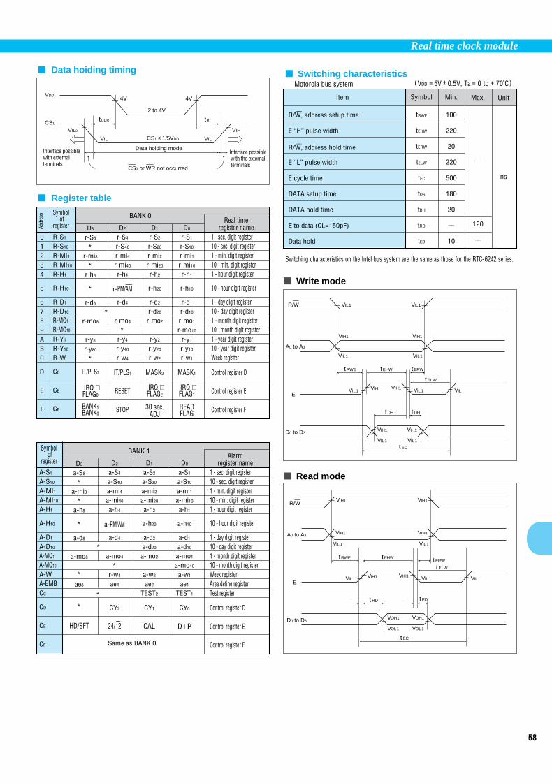
58
Real time clock module
R/W
E
A0 to A3
D0 to D3
CS1
CS0 or WR not occurred
CS1 1/5VDD
VDD4V 4V
VIL2 VIH
VIL VIL
tCDR tR
2 to 4V
≤
Data holding modeInterface possiblewith external terminals
Interface possible with the external terminals
Read mode
Write mode
Data hoiding timing Switching characteristics
Register table
t EC
t ELW
tERWtEHWtRWE
t DS t DH
VIL1
VIL1
VIL1
VIL1 VIL1
VIL1
VIL1 VIL
VIH1
VIH1 VIH1
VIH1VIH
VIH1
VIL1
R/W
E
A0 to A3
D0 to D3
t EC
t ELW
tERWtEHWtRWE
t RD t ED
VOL1
VIL1
VIL1
VIH1 VIH1
VIL1
VIL1 VIL
VOH1
VOL1
VOH1
VIH1 VIH1
VIH1VIH1
(VDD = 5V ± 0.5V, Ta = 0 to + 70˚C)Motorola bus system
Switching characteristics on the Intel bus system are the same as those for the RTC-6242 series.
01234
5
6789ABC
D
E
F
Symbolof
registerR-S1
R-S10
R-MI1
R-MI10
R-H1
R-H10
R-D1
R-D10
R-MO1
R-MO10
R-Y1
R-Y10
R-W
CD
CE
CF
D3
r-S8
∗r-mi8
∗r-h8
∗
r-d8
r-mo8
r-y8
r-y80
∗
IT/PLS2
IRQ ⋅FLAG0
BANK1BANK0
D2
r-S4
r-S40
r-mi4r-mi40
r-h4
___r-PM/AM
r-d4
r-mo4
∗r-y4
r-y40
r-w4
IT/PLS1
RESET
STOP
D1
r-S2
r-S20
r-mi2r-mi20
r-h2
r-h20
r-d2
r-d20
r-mo2
r-y2
r-y20
r-w2
MASK2
IRQ ⋅FLAG2
30 sec.ADJ
D0
r-S1
r-S10
r-mi1r-mi10
r-h1
r-h10
r-d1
r-d10
r-mo1
r-mo10
r-y1
r-y10
r-w1
MASK1
IRQ ⋅FLAG1
READFLAG
Real timeregister name
1 - sec. digit register10 - sec. digit register1 - min. digit register10 - min. digit register1 - hour digit register
10 - hour digit register
1 - day digit register10 - day digit register1 - month digit register10 - month digit register1 - year digit register10 - year digit registerWeek register
Control register D
Control register E
Control register F
Item
__R/W, address setup time
E “H” pulse width
__R/W, address hold time
E “L” pulse width
E cycle time
DATA setup time
DATA hold time
E to data (CL=150pF)
Data hold
Symbol
tRWE
tEHW
tERW
tELW
tEC
tDS
tDH
tRD
tED
Min.
100
220
20
220
500
180
20
––
10
Max.
––
120
––
Unit
ns
Addr
ess BANK 0
Symbolof
registerA-S1
A-S10
A-MI1
A-MI10
A-H1
A-H10
A-D1
A-D10
A-MO1
A-MO10
A-WA-EMBCC
CD
CE
CF
D3
a-S8
∗a-mi8
∗a-h8
∗
a-d8
a-mo8
∗ae8
∗
HD/SFT
D2
a-S4
a-S40
a-mi4a-mi40
a-h4
___a-PM/AM
a-d4
a-mo4
∗r-w4
ae4
CY2
__24/12
D1
a-S2
a-S20
a-mi2a-mi20
a-h2
a-h20
a-d2
a-d20
a-mo2
a-w2
ae2
TEST2
CY1
CAL
D0
a-S1
a-S10
a-mi1a-mi10
a-h1
a-h10
a-d1
a-d10
a-mo1
a-mo10
a-w1
ae1
TEST1
CY0
D ⋅ P
Alarmregister name
1 - sec. digit register10 - sec. digit register1 - min. digit register10 - min. digit register1 - hour digit register
10 - hour digit register
1 - day digit register10 - day digit register1 - month digit register10 - month digit registerWeek registerArea define registerTest register
Control register D
Control register E
Control register F
BANK 1
Same as BANK 0
∗
∗
∗
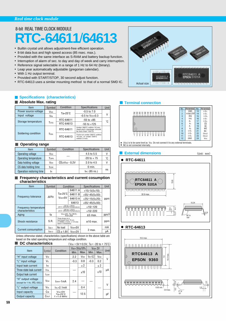
59
Real time clock module
Specifications (characteristics) Absolute Max. rating
Operating range
Frequency characteristics and current cosumption characteristics
DC characteristics
External dimensions
Terminal connection
(Unit: mm)
RTC-64611
RTC64613 A
EPSON 9360
RTC64611 AEPSON 5101A
(VDD) is to be same level as VDD. Do not connect it to any external terminals. NC is not connected internally.
1
24
2
23
3
22
4
21
5
20
6
19
7
18
8
17
9
16
10
15
11
14
12
13
RTC-64613
32.0 max.
13.6
4.4
3.3
0.8
15.24
0.25
2.5
16.3 max.
7.9
12.2
max
.
1.0
0.3
0.2
Unless otherwise stated, characteristics (specifications) shown in the above table arebased on the rated operating temperature and voltage condition.
(VDD = 5V ± 0.5V, Ta = -20 to + 75˚C)
No.123456789
101112
No.131415161718192021222324
GND H-START/STOP
IRQ 1HZ
A3
A2
A1
A0
I /O 1
I /O 2
I /O 3
GND
Pin terminal I /O 4
I /O 5
I /O 6
I /O 7
I /O 8
CS OE WENC
(VDD)(VDD) VDD
Pin terminal
0° to 10°
90° to105°
0.05 min.2.8 max.
8-bit REAL TIME CLOCK MODULE
RTC-64611/64613• Builtin crystal unit allows adjustment-free efficient operation.• 8-bit data bus and high speed access (85 nsec. max.).• Provided with the same interface as S-RAM and battery backup function.• Interruption of alarm of sec. to day and day of week and carry interruption.• Reference signal selectable in a range of 1 Hz to 64 Hz (binary).• Leap year automatically adjustable (gregorian calendar).• With 1 Hz output terminal.• Provided with START/STOP, 30 second adjust function.• RTC-64613 uses a similar mounting method to that of a normal SMD IC.
ItemPower source voltage
Input voltage
Storage temperature
Soldering condition
Symbol
VDD
VIN
TSTG
TSOL
Condition
Ta=25˚C
RTC-64611RTC-64613
RTC-64611
RTC-64613
Specifications
-0.5 to 7.0
-0.5 to VDD+0.3
-55 to +85
-55 to +125Under 260˚C within 10 sec. (lead part) (package shouldbe less than 150˚C)
Twice at under 260˚C within 10 sec. or under 230˚Cwithin 3 min.
Unit
V
˚C
Item
Operating voltageOperating temperatureData holding voltageCS data holding timeOperation restoring time
Symbol
VDD
TOPR
VDH
tCDR
tR
Condition
—
CS ≥VDD - 0.2V
Specifications
4.5 to 5.5
-20 to + 75
2.0 to 4.5
0 min.
tRC (85 ns.)
Unit
V
˚C
V
ns
Item
Frequency tolerance
Frequency temperature characteristicsAging
Shock resistance
Current consumption
Symbol
∆f/fo
fa
S.R.
IDD 1
IDD 2
Ta=25˚CVDD=5V
64611 A
64611 B
64613 A
64613
Condition
Three drops on a hard board from 75 cmor 3000G x 0.3ms x 1/2 sinewave x 3 directions
No load__CS ≥ 1.8V
VDD=5V
VDD=2V
Specifications
+15/-5(5±10)+55/-45(5±50)+25/-15(5±20)+55/-45(5±50)
+10/-120+10/-220±5 max.
±10 max.
2 max.
Unit
ppm
ppm/Y
ppm
mAµA
-10 to +70˚C(25˚C reference temperature)
-20 to +75˚C(25˚C reference temperature)
VDD=5V, Ta=25˚C, first year
Item
“H” input voltage
“L” input voltage
Input leak current
Three-state leak currentOutput leak current“H” output voltage___(except for 1 Hz, IRQ, OSC2)
“L” output voltage
Input capacity
Output capacity
S y m b o l
VIH
VIL
IIN
ITSL
ILOH
VOH
VOL
CIN
COUT
Condition
IOH=-1mA
IOL=2.1mA
VIN=OVTa=25˚C
f =1.0 MHz
Min.
2.2
-0.3
—
2.4
—
Max.
VDD
0.8
± 2
±10
—
0.4
12.5
Unit
V
µA
V
pF
Min.
VDD -0.2-0.3
—
Max.
VDD
0.2
± 2
±10
—
VDD= 5V±10% VDD= 2V
Actual size

60
Real time clock module
OSC32.768 KHZ
Read mode
Write mode
Switching characteristic Register table
Block diagram
Supplement
16 KHz
2 KHz
32 Hz
8 KHz
1 KHz
16 Hz
4 KHz
512 Hz
8 KHz
256 Hz
4 Hz
128 Hz
2 Hz
64 Hz
64 Hz register / counter
64 Hz alarm. register
Alarm
comparison circuitSec. alarm. register
Min. alarm. register
Hour alarm. register
Day-of-week alarm. register
Day alarm. register
Control register A
Control register B
Sec. register / counter
Min. register / counter
Hour register / counter
Day-of-week register / counter
Day register / counter
Month register / counter
Year register / counter
1 Hz 1 Hz
H • START / STOP
Write
Read
Data bus
Bus interface circuit
I/01 to I/03
Address busA0 to A3 CS OE WE
IRQ
Address
OE
CS
DOUTData valid
tRC
tAA
tACS
tOH
tOHZ
tOHZ
tCHZ
tOE
tOLZ
tOH
VOL
VOL VOL
VOL
OE
CS
DOUT
DIN
Address
tWC
tCW
tAW
tW-R
tAS
tOHZ
WE
tWP
tDW tDH
Measuring condition
Input pulse level: 0.8 to 2.4V
Input risetime, falltime: 5 nsec.
IN/OUT timing pulse level: 1.5V
Out put loard: 1 TTL Gate +100pF
Note: Do not enter erroneous data for clock. This may result in time keeping error.
Be sure to enter “O” to TEST bit.∗1
0123456789ABCD
E
F
b7
∗
Addr
ess Data
b6
1 Hzb5
2 Hzb4
4 Hzb3
8 Hzb2
16 Hzb1
32 Hzb0
64 Hz10-sec. digit10-min. digit
1-sec. digit1-min. digit1-hour digit10-hour digit∗
∗∗
∗
∗
∗
∗ ∗
10-day digit10-monthdigit
10-year digit
1 Hz 2 Hz 4 Hz 8 Hz 16 Hz 32 Hz 64 Hz
ENB
Carryflag
RAM7 RAM6 RAM5 RAM4 TEST∗ 1 30-sec.
adjustment RESET S.START/STOP
Alarmflag
Carryinterruptionenable
Alarminterruptionenable
10-sec. digit10-min. digit
10-hour digit∗
10-day digit
Day-of-week digit1-day digit1-month digit1-year digit
1-sec. digit1-min. digit1-hour digitDay-of-week digit
1-day digit
Remarks
Counter
Alarmregister
Controlregister
Bit name
∗ mark
10-hour digit (b5)
Under-sec.counter
Under-sec.alarm register
Sec.to year
Day of week
Description
Empty bit and unwritableRecognized as “0” while reading
Only for 24H mode
Read only (unwritable)Used as binary code data
Used as binary code data
Both counter and alarm register use BCD code
Coded data is usedEX: 0…Sunday 1…Monday 2…Tuesday 3…Wednesday
4…Thursday 5…Friday 6…Saturday
Item
Read cycle time
Address access time
Chip select access time
Output enable access time
Output hold time
Chip select / output set time
Output enable / output set time
Chip deselect / output floating
Output disable / output floating
Symbol
tRC
tAA
tACS
tOE
tOH
tCLZ
tOLZ
tCHZ
tOHZ
Min.
85
—
10
5
0
Max.
—
85
45
—
35
Unit
ns
Item
Write cycle time
Chip select time
Address valid time
Address setup time
Write pulse time
Address holding time___WE output floating
Input data set time
Input data hold time
Output disable / output floating___WE output set time
Symbol
tWC
tCW
tAW
tAS
tWP
tWR
tWHZ
tDW
tDH
tOHZ
tOW
Min.
85
75
0
60
10
0
40
0
5
Max.
—
35
—
35
—
Unit
ns

61
Real time clock module
External dimensions
Terminal connection
(Unit: mm)
NC is not connected internally.
1
28
2
27
3
26
4
25
5
24
6
23
7
22
8
21
9
20
10
19
11
18
12
17
13
16
14
15
Specifications (characteristics) Absolute Max. rating
Operating conditions
Frequency characteristics
DC characteristics
∗1
∗
Storage temperature as a discrete component.
(VDD = 5.0V ± 10%, Ta = -10 to + 70˚C)
1: The frequency deviation (Oppm) at Ta=25˚C for “top” or at VDD =5V for “fv” is used as the reference value.
Note: For information on handling batteries, please independently refer to the pertinent requlations, as this product does not come equipped with batteries.
No.123456789
1011121314
No.1516171819202122232425262728
A0
A1
TMODETCLOCK
STBYD0
D1
D2
D3
D4
D5
D6
D7
GND
Pin TerminalRTC
XRAMWR NCRD
RESETIRQNCA5
A4
SQWVDD
A3
A2
Pin Terminal
36.8 max.
14.6
9.0
max
.0.
83.
3
15.24
15.24 to 18.02.54
RTC65271 5201C
E
8-bit REAL TIME CLOCK MODULE
RTC-65271• Builtin crystal unit allows adjustment-free efficient operation.• A builtin power supply switching circuit makes it possible to provide automatic
power supply backup to both the RTC and extended RAM.• The real-time clock block consists of:
Indirect register: 1-byte Control register: 4-bytesClock, alarm, calendar: 10-bytes User RAM: 50-bytes
• Extended RAM: 4K-bytes of builtin S-RAMPage register: 1-byte Configuration: 32-bytes x 128 pages
• The package is a 28-pin DIP IC with a battery holder that makes batteryreplacement possible.
• Batteries (BR1225) are available as an option. (Batteries are packed separatelyfrom the RTC.)
Item
Supply voltage
Input voltage
Storage temperature
Soldering condition
Symbol
VDD
VIN
TSTG
TSOL
Condition
VDD - GND
Input Pin
∗ 1
Unit
V
˚C
Item
Supply voltage
Operating temperature
Symbol
VDD
TOPR
Condition
-------
Item
Frequency tolerance
Temperature characteristics
Voltagecharacteristics
Aging
Symbol
∆f/fo
TOP
fv
fa
Ta=25˚C, VDD=5V
Ta=-10 to 70˚C, VDD=5V∗ 1
Ta=stable, VDD=3V∗ 1
Ta=25˚C, VDD=5V, first year
Condition
Item
Input voltage
Input leak current
Output voltage
Power supply current
Current when usingbattery backup
Input current
Symbol
VIH
VIL
II
VOH
VOL
IDD
IBAT
ISTBY
Condition
——
______ ___ ___ ____RESET,RD, WR, RTC, ______XRAM, D0 to D7, A0 to A5
VDD=5V, ILOAD=-4mA
VDD=5V, ILOAD=4mA
Output unloaded
Ta=25˚C______STBY=GND
Max.
VDD+0.3
0.8
±1
—
0.4
15
1.0
2
Unit
V
µA
V
mA
µA
Min.
2.2
-0.3
—
2.4
—
Min.
-0.3
-40
Max.
+7.0
VDD+0.3
+85
260˚C or less, for 10 seconds or less;(package should be 150˚C or less)
Unit
V
˚C
Min.
4.5
-10
Max.
5.5
+70
Typ.
5.0
—
Max.
5±20
+10-120
±5
±5
Unit
ppm
ppm/year
Typ.
—
0.5
—
Actual size
Batteries in this photograph are used only to show the inserted condition. This RTC is not supplied with the batteries inserted.

62
Real time clock module
INDIRECT ADDRESS REG
RTC DATA REGISTER
14-bytesRTC
14-bytesREAL TIME CLOCK
50-bytesUSER-RAM
INDIRECTADDRESS
00 00 00
01
02
03
04
05
06
07
08
09
0A
0B
0C
0D
0D
0E
3F3F
SECONDS
SECOND ALARM
MINUTES
MINUTE ALARM
HOUR ALARM
HOURS
DAY OF WEEK
DAY OF MONTH
MONTH
YEAR
REGISTER A
REGISTER B
REGISTER CREGISTER D
128 PAGESOF 32-bytesEXTENDED RAM
PAGE 7F
0201
PAGE 00
XRAM
XRAM PAGE REGISTER
XRAM + 1F
XRAM + 3F
XRAM + 20
XRAM + 21
THRU
THRU ALIASES OFPAGE REGISTER
AO to A5
RTC
VALID
VALID
VALID
XRAM
WR
DATA BUSWRITE
(DO to D7)DATA
DATA
RD
DATA BUS
READ(DO to D7)
tCYC
t F
t Ft CWS
t DSW
tCH
tAH
tDHW
tAWSt RWL
t R
t R
t CRS tCH
tDHR
tAH
tARS
PWRWL
t DDR
TCLOCK
TMODE
VDD
BUSINTERFACE
STBY
DO to D7
RD
WR
A0 to A5
A0 to A4
RTC
XRAM
SELECTOR
50%DUTY8.192 KHz
OSC
ON / OFF
POWERSWITCHINGREFERENCE
POK
VPP
CE
DATA / CONTROL
DIVIDER CHAIN13 TAPS TO SELECTOR
PERIODIC INTR / SQ WAVE SELECTOR
RS0 to RS3
DE
CO
DE
R
RE
GIS
TE
R IN
DE
X
410
1
3
3
REGISTERSA,B,C,D
CLOCK, CALENDAR, AND ALARMREGISTERS
COLUMN DECODER, 1 of 8
50-bytes USER-RAM
ROW DECODER, 1 of 8
ROW DECODER, 1 of 32
DV0 to DV2SQW
RESET
IRQ
CLOCK
CALENDAR
UPDATE
EXTENDED RAM REGISTER
EXTENDED RAM4096-bytes
COLUMN DECODER, 1 of 128
Switching characteristics Timing chart
Address map
Block diagram
RTC address map Extended RAM address map
(VDD = 5V ± 10%, GND =0V, Ta = -10 to +70˚C)Item
Cycle Time
Pulse width RD__
/WR__
=“L” interval
Signal rise / fall time CS, RD__
, WR__
Address holding time
Address setup before RD__
Address setup before WR__
Chip select setup time before RD__
Chip select setup time before WR__
Chip select hold time a after RD__
/WR__
Read data holding time
Write data holding time
RD__
Peripheral output data delay timePeripheral write data setup time
Symbol
tCYC
tRWL
tR, tF
tAH
tARS
tAWS
tCRS
tCWS
tCH
tDHR
tDHW
tDDR
tDSW
Min.
395
325__
20
50
0
50
0
20
10
0
20
200
Max.
DC
30
100
240
Remarks
ns__
__
__
__

63
Real time clock module
Terminal Pin NoAD0
AD1
AD2
AD3
AD4
AD5
AD6
AD7
456
7
89
1011
Specifications (characteristics) Absolute Max. rating
Operating range, frequency and DC characteristics
(Unit: mm)
1 12
1324
16.3 max.
7.9
12.2
max
.1.0
0° to 10°
0.2
2.8
max
.
0.0
5min
.
External dimensions
Terminal functions
RTC6593EPSON 5200B
REAL TIME CLOCK MODULE FOR PC/AT
RTC-6593• Builtin crystal unit allows adjustment-free efficient operation.• Provides 114-bytes of backed-up RAM.• Extended alarm function.• Low current consumption.• A builtin power supply switching circuit makes it possible to provide
automatic power supply backup to both the RTC and extended RAM.
Item
Supply voltage
Input voltage
Storagetemperature
Solderingconditions
Symbol
VDD
VIN
TSTG
TSOL
Condition
VDD-GND
Input pin
—
Rating
- 0.3 to + 7.0
- 0.3 to VDD + 0.3
- 55 to+125
Unit
V
˚C
Twice under 260˚C within 10seconds or under 230˚Cwithin 3 minutes
Item
Supply voltage
Operatingtemperature
Frequencytolerance
Temperature characteristics
Voltagecharacteristics
Aging
Symbol
VDD
TOPR
∆f/fo
Top
fv
fa
VIH
VIL
VOH
VOL
IDD
IBAT
VDD - GND
—
Ta=25˚C, VDD=5V
Ta=-10 to 70˚C25˚C standard
Ta=stable
Ta=25˚C, VDD=5VFirst year
—
VDD=5VILOAD=-4mA
VDD=5VILOAD=+4mA
Outputunloaded
VBAT=3VVDD= 0V
Condition Min.
4.5
-10
—
2.2
-0.3
2.4
Unit
V
˚C
ppm
ppm/V
ppm/Y
V
mA
µA
Inputvoltage
Outputvoltage
High level
Low level
High level
Low level
Power supplycurrent
Battery supplycurrent
Typ.
5.0
—
3
0.5
Max.
5.5
+70
5±20
+10-120
±6
±5
VDD+0.3
0.8
0.4
10
1.0
Terminal
MOT
AD0 to 7
GND
RTC___
AS
R/W_
DS
RESET_____
IRQ___
VBAT
XIRQ____
XALM____
SQW
VDD
NC
Function
Model select (input)
Multiplexed bi-directionaddress/data buses
Power supply (grand)
Real time clockselect (input)
Address strobe (input)
Read/ Write (input)
Data strobe (input)
Reset (input)
Interrupt request (output)
Back-up power supply
Extended alarminterrupt request (output)
Extended alarmselect (input)
Square wave output
Power supply (+5V)
Not connected internally
Pin No.
1
4 to 11
12
13
14
15
17
18
19
20
21
22
23
24
2,3,16
—
∗ 1
Actual size *1 PC/AT is a trademark of International Business Machines Corporation.
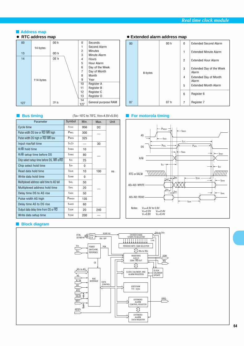
64
Real time clock module
Address map
Block diagram
Bus timing For motorola timing
RTC address map Extended alarm address map
VBAT
VDD
XTAL32768 Hz
BUSINTERFACE
OSC1/4 ON / OFF
POWERSWITCHINGREFERENCE
DIVIDER CHAIN13TAPS TO SELECTOR
PERIODIC INTR / SQW SELECTOR
RS0 to RS3
REGISTERSA,B,C,D
SQW / IRQ OUT
CLOCK, CALENDER, AND ALARM REGISTERS
USER RAM114 - bytes
DV0 to DV2
SQW
RESET
IRQ
CLOCKCALENDERUPDATE
EXTENDEDALARM
CONTROL REGISTER
EXTENDEDALARM
DATA REGISTER
8190 Hz
POK
1 Hz
DATA CONTROL
AD0 to AD7
AS
CE
R / W
DS
RTC
XALMXIRQ
MOT
PWASHtASED
tASD
tCS
tRWS
tDSW
tDDR
tDHR
tDHW
tAHL
tAHL
tASL
tASL
tRWH
tCH
tCYC
PWEL PWEHDS
AD0-AD7 WRITE
AD0-AD7 READ
Notes: VDD=4.5V to 5.5VVIH=2.2V VOH=2.4VVIL=0.8V VOL=0.4V
XALM
R/W
AS
RTC or
00
13
14
127
14-bytes
114-bytes
00 h
0D h
OE h
7F h
01234567891011121314127
SecondsSecond AlarmMinutesMinute AlarmHoursHour AlarmDay of the WeekDay of MonthMonthYearRegister ARegister BRegister CRegister D
General purpose RAM
Parameter
Cycle time
Pulse width DS low or RD__
/ WR__
high
Pulse width DS high or RD__
/ WR__
low
Input rise/fall time
R/W_
hold time
R/W_
setup time before DS
Chip select setup time before DS, WR__
orRD__
Chip select hold time
Read data hold time
Write data hold time
Multiplexed address valid time to AS fall
Multiplexed address hold time
Delay time DS to AS rise
Pulse width AS high
Delay time AS to DS rise
Output data delay time from DS or RD__
Write data setup time
Symbol
t CYC
PWEL
PWEH
tR,t F
t RWH
tRWS
tCS
tCH
tDHR
tDHW
tASL
tAHL
t ASD
PWASH
tASED
tDDR
tDSW
Min.
956
300
325
—
10
80
25
0
10
0
50
20
50
135
60
20
200
Max.
DC
—
30
—
100
—
240
—
Unit
ns
00
07
8-bytes
0
1
2
3
4
5
6
7
00 h
07 h
Extended Second Alarm
Extended Minute Alarm
Extended Hour Alarm
Extended Day of the Week Alarm
Extended Day of Month AlarmExtended Month Alarm
Register 6
Register 7
(Ta=-10˚C to 70˚C, VDD=4.5V+5.5V)
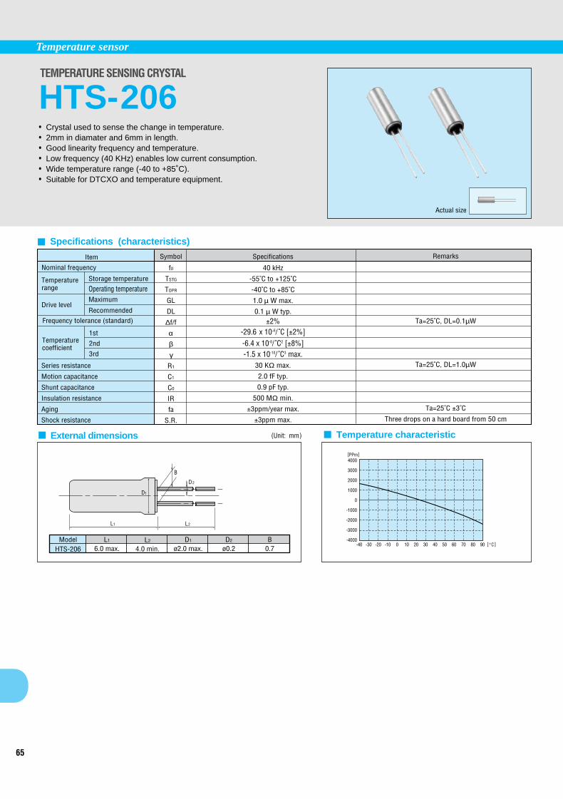
65
Temperature sensor
D1
L1 L2
B
D2
(Unit: mm) External dimensions
-40-4000
-3000
-2000
-1000
0
1000
2000
3000
4000
-30 -20 -10 0 10 20 30 40 50 60 70 80 90 [°C]
[PPm]
Specifications (characteristics)
Temperature characteristic
TEMPERATURE SENSING CRYSTAL
HTS-206• Crystal used to sense the change in temperature.• 2mm in diamater and 6mm in length.• Good linearity frequency and temperature.• Low frequency (40 KHz) enables low current consumption.• Wide temperature range (-40 to +85˚C).• Suitable for DTCXO and temperature equipment.
Item
Nominal frequency
Temperaturerange
Drive level
Frequency tolerance (standard)
Storage temperature
Operating temperatureMaximum
Recommended
Temperaturecoefficient
1st
2nd
3rd
Series resistance
Motion capacitance
Shunt capacitance
Insulation resistance
Aging
Shock resistance
Symbol
f0
TSTG
TOPR
GL
DL
∆f/f
αβγ
R1
C1
C0
IR
fa
S.R.
Specifications
40 kHz
-55˚C to +125˚C
-40˚C to +85˚C
1.0 µ W max.
0.1 µ W typ.±2%
-29.6 x 10⁻⁶/ ˚C [±2%]-6.4 x 10⁻⁸/ ˚C2 [±8%]-1.5 x 10⁻¹⁰/ ˚C3 max.
30 KΩ max.
2.0 fF typ.
0.9 pF typ.
500 MΩ min.
±3ppm/year max.
±3ppm max.
Remarks
Ta=25˚C, DL=0.1µW
Ta=25˚C, DL=1.0µW
Ta=25˚C ±3˚C
Three drops on a hard board from 50 cm
ModelHTS-206
L1
6.0 max.L2
4.0 min.D1
ø2.0 max.D2
ø0.2B
0.7
Actual size
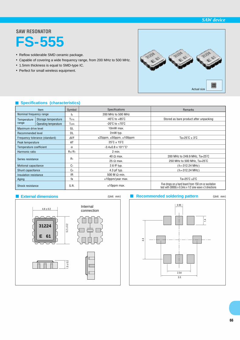
66
SAW device
4.8 ± 0.2
5.2
± 0.
21.
5 ±
0.2
(Unit: mm) (Unit: mm) External dimensions
Specifications (characteristics)
Recommended soldering pattern
31224
61E
Internalconnection
3.5
2.54
0.95
4.4
1.4
SAW RESONATOR
FS-555• Reflow solderable SMD ceramic package.
• Capable of covering a wide frequency range, from 200 MHz to 500 MHz.
• 1.5mm thickness is equal to SMD-type IC.
• Perfect for small wireless equipment.
Item
Nominal frequency range
Temperaturerange
Storage temperature
Operating temperatureMaximum drive level
Recommended level
Frequency tolerance (standard)
Peak temperature
Temperature coefficient
Harmonic ratio
Series resistance
Motional capacitance
Shunt capacitance
Insulation resistanceAging
Shock resistance
Symbol
f0
TSTG
TOPR
GL
DL
∆f/f
θT
αRS/R1
R1
C1
C0
IRfa
S.R.
Specifications
200 MHz to 500 MHz
-40˚C to +85˚C
-20˚C to +70˚C
10mW max.
2mW typ.
±25ppm, ±50ppm, ±100ppm
25˚C ± 15˚C
-3.4±0.8 x 10⁻⁸/ ˚C2
2 min.
40 Ω max.
25 Ω max.
2.6 fF typ.
4.3 pF typ.500 M Ω min.
±10ppm/year max.
±10ppm max.
Remarks
Stored as bare product after unpacking
Ta=25˚C ± 3˚C
200 MHz to 249.9 MHz, Ta=25˚C
250 MHz to 500 MHz, Ta=25˚C
(f0=312.24 MHz)
( f0=312.24 MHz)
Ta=25˚C ±3˚C
Five drops on a hard board from 150 cm or excitation test with 3000G x 0.3ms x 1/2 sine wave x 3 directions
Actual size

67
Glossary
Duty=tw/t × 100% Duty=tw/t × 100%
tTLH tTHL
VOLVOH
ttW
80%VDD
VDD
20%VDD
GND
1/2VDD
tTLH tTHL
VOLVOH
ttW
2.4V
VDD
0.4V
GND
1.4V
X'tal: Crystal unit, OSC: Crystal oscillator, RTC: Real time clock module
C-MOS loading TTL loading
Item Content
Tuning fork crystal unit AT crystal unit
Object
Fundamental mode
Fundamental mode 3rd overtone mode
First harmonic crystal vibration mode.The AT resonance frequency is determined by thethickness of the crystal, but even with the same thicknessthe third overtone will be about three times the frequencyof the fundamental. With tuning fork crystal unit, thesecond overtone is about six times the fundamental.
Fundamental mode
Baud rate
Divided frequency
(Equivalent) seriescapacitance (C1)(motional capacitance)
(Equivalent) seriesresonant resistance
(R1)
Drive level (DL)
Frequency (f0)
Frequency toleranceprecision (∆f/f)
Frequency stability(∆f/fo)
(Frequency) aging (fa)
Duty (tw/t)(symmetry)
AT fundamental mode
f (MHz) = t (µm)
1670
The rate of data transmission, i.e. how many data can be transmitted in one second.
The output frequency that is divided by the internal IC.
Ratio of full and half cycles. For C-MOS loading duty is rated at 1/2VDD, and for TTL loading at 1.4V.
Energy distortion to the (equivalent) internal charge capacitance component of the crystal unit,at the series resonant frequency.
Vibration loss to the (equivalent) internal resistance component of the crystal resonator, at theseries resonant frequency. A measure of the easiness of oscillation.
Number of waves (cycles) per second. The relation between frequency and cycle is f0 (Hz) =1/t(sec). 1 kHz=1ms, 1 MHz=1 µs, 1 GHz=1ns.
Amount of frequency drift when operated under the specified conditions for a specified term.
Under specified conditions at an ambient temperature of 25˚C, the difference in actual(measured) frequency from the nominal frequency.
Within standard temperature and operational voltage ranges, the drift in the output frequency.The output frequency drift including frequency temperature characteristics and frequencyvoltage characteristics.
Current or voltage level in the oscillating (operating) state. (Drive power=power required tooscillate crystal unit.)
OSC
ALL
ALL
ALL
X' tal
X' tal
X' tal
OSC
OSC
OSC
X'tal,OSC

68
Item Content Object
0
-10
-20
-30
-40
-50
-60
-70
-20 -10 0 10 20 30 40 50 60 70 -40
-60
-40
-20
0
20
40
-20 0 20 40 60 80 100
Temperature (˚C)
Tuning fork crystal units
Examples of frequency temperature characteristics
Temperature (˚C)
AT-cut crystal units
Freq
uenc
y
∆f/f
(ppm
)
Freq
uenc
y
∆f/f
(ppm
)
Typical T=25˚Ca=-0.035ppm/˚C 2
X'tal: Crystal unit, OSC: Crystal oscillator, RTC: Real time clock module
θ
Taking the frequency at 25 degrees Centigrade as the reference, the change in frequency in
response to ambient temperature.
• Tuning fork crystal unit.
∆ f/f (ppm) =a (θ T- θX) 2
, θ X: specified temperature
• AT crystal unit.
∆ f/f=α (θ -25) +β (θ -25)2
+ γ (θ -25) 3
Taking the output frequency at the central voltage in the operating voltage range as thereference, the change in output frequency to voltage. Causes of this change are changes incrystal deformation, and changes in IC internal constants for chips mounted in the oscillatorand RTC. The effects of the ICs are larger.
Resistance between lead and lead, or between lead and case package. (conductive package)
Effective capacitance (series equivalent charge capacitance) of the oscillation circuit as seenfrom the pins of the crystal unit. This capacitance is determined as a condition when thecrystal unit is connected to the oscillation circuit and will determine the output frequency. Loadcapacitance approximation: CL ≠ CG × CD/ (CG+CD) + CS
(CS=stray capacitance)
Rating for the drive level. Current or power input over this level may result in characteristicdegradation or destruction.
Maximum rated value for power input to the power supply pin. Input over this value may resultin characteristic degradation or destruction.
Nominal value of frequency of crystal unit.
Temperature range where specification characteristics are fulfilled, unless otherwisespecified.
Voltage input to VDD pin which will support continuous operation with specificationcharacteristics.
Oscillation source frequency of oscillator inside oscillation system.
Frequency temperaturecharacteristics
Frequency voltagecharacteristics
Insulation resistance(IR)
Load capacitance(CL)
Max. drive level (GL)
Max. supply voltage(VDD-GND)
Nominal frequency (f)
Operating temperaturerange (TOPR)
Operating voltage(VDD)
Origin frequency (f0)
OSC,RTC
OSC,RTC
OSC,RTC
OSC
ALL
ALL
ALL
X' tal
X' tal
X' tal

69
Item Content Object
X'tal: Crystal unit, OSC: Crystal oscillator, RTC: Real time clock module
Basic oscillation circuit using C-MOS IC
Timing
RD
Rf
X'tal
CDCG
tPZLtPZH
VIH
VIL
OE Enabled
OUTPUTHigh impedance
Disabled
Timing
tPHLtPLH
VIL
VOH
Low level
VIH
Stand-by
OUTPUT
ST
Function that halts crystal unit oscillation and frequency division. Cuts the current consumed by theoscillators circuit and the frequency division stage. ST pin - high or open: Specified frequencyoutput.ST Pin - low: Output is low level, clock stops. Because oscillation is halted, If ST is alsodropped to low, output is high impedancebut output is also unstable after function isrestarted, for the same reason.
Circuit needed to oscillate crystal unit. Circuitconstants will differ with type of crystal unit andfrequency.
The time from power on until the waveformstabilizes. However, voltage rise times depend onthe power supply, therefore the time is measuredfrom a specific set of initial conditions.
Output is switched to high impedance,and wired OR connection can be used toselect multiple outputs (frequency).
OE pin:
OE pin:
Oscillation is not stopped, so the clock afterdisabled is cleared is not synchronized withOE (clock is continuous).
High or open. Specified frequencyoutput = enabled.Low. Output is high impedance= disabled.
The time it takes for the output waveform to change from the high voltage (high level) to thelow voltage (low level). Also called waveform fall time. See waveform diagram under duty.
The types and quantities (power) of the loads that can be connected to the oscillator. Calculatedfor 1 TTL as lOH=-40 µA, lOL=1.6mA and for LS-TTL as IOH=-20 µA, lOL,=0.4mA, 1 C-MOS=5pF.
The time it takes for the output waveform to change from the low voltage (low level) to the highvoltage (high level). AIso called waveform rise time. See waveform diagram under duty.
Vibration state when crystal in vibrating as a high harmonic (see base wavelength). It is harderto match the overtone oscillation circuit with the crystal unit than the fundamental oscillationcircuit.
Excitation level for optimum oscillation characteristics.
Soldering conditions that can be assured at mounting. Temperatures or times over these limitsmay result in characteristic degradation or destruction.
Maximum absolute rating for the discharged state (no input of voltage, current or power).Exposure to temperatures over this level may result in characteristic degradation ordestruction. To assure precision, store at room temperature whenever possible.
Charge capacitance between the two electrodes in the crystal unit.
The frequency output from the oscillator circuit or the crystal oscillator system.
Oscillation circuit
Oscillation start up time(tOSC)
Output enable (OE)
Output fall time (tTHL)
Output frequency (fo)
Output load conditions (N or CL)
Output rise time (tTLH)
Recommendeddrive level (DL)
Soldering conditions(TSOL)
Stand-by (ST)
Storage temperaturerange (TSTG)
Overtone
Shunt capacitance (C0)
OSC,RTC
OSC
OSC
OSC
OSC
OSC
OSC,RTC
ALL
ALL
X' tal
X' tal,OSC
X' tal
X' tal

70
Electronic Device Information on WWW serverSeiko Epson is providing the Electronic Devices Information, Semiconductor, Liquid Crystal Display,
Crystal Products and more. Please access here !
Seiko Epson Home Page
http://www.epson.co.jp
Japanese Home Page Ehglish Home Page (http://www.epson.co.jp/epson/weleng.htm)
Electronic Device Index Page
Entrance of Electronic Devices Information
Lineup Page for each device
Catalog & Data Sheet Page
Introduce the lineup of each device.
Catalogs and Data sheets for each devices are available.

71
Product Inquiry by E- Mail
Seiko Epson receives your inqurties on the products througy e- mail. Your inquiry is welcome at Seiko Epson.Mail address:[email protected]

Issued on Sep.,1997
Electronic Devices Marketing Dept.SEIKO EPSON CORPORATION